KR20220008319A - 저유전율 필름 및 이의 제조 방법 - Google Patents
저유전율 필름 및 이의 제조 방법 Download PDFInfo
- Publication number
- KR20220008319A KR20220008319A KR1020217040802A KR20217040802A KR20220008319A KR 20220008319 A KR20220008319 A KR 20220008319A KR 1020217040802 A KR1020217040802 A KR 1020217040802A KR 20217040802 A KR20217040802 A KR 20217040802A KR 20220008319 A KR20220008319 A KR 20220008319A
- Authority
- KR
- South Korea
- Prior art keywords
- compound
- gpa
- low
- film
- dielectric constant
- Prior art date
- Legal status (The legal status is an assumption and is not a legal conclusion. Google has not performed a legal analysis and makes no representation as to the accuracy of the status listed.)
- Abandoned
Links
Images

Classifications
-
- B—PERFORMING OPERATIONS; TRANSPORTING
- B05—SPRAYING OR ATOMISING IN GENERAL; APPLYING FLUENT MATERIALS TO SURFACES, IN GENERAL
- B05D—PROCESSES FOR APPLYING FLUENT MATERIALS TO SURFACES, IN GENERAL
- B05D1/00—Processes for applying liquids or other fluent materials
- B05D1/62—Plasma-deposition of organic layers
-
- C—CHEMISTRY; METALLURGY
- C23—COATING METALLIC MATERIAL; COATING MATERIAL WITH METALLIC MATERIAL; CHEMICAL SURFACE TREATMENT; DIFFUSION TREATMENT OF METALLIC MATERIAL; COATING BY VACUUM EVAPORATION, BY SPUTTERING, BY ION IMPLANTATION OR BY CHEMICAL VAPOUR DEPOSITION, IN GENERAL; INHIBITING CORROSION OF METALLIC MATERIAL OR INCRUSTATION IN GENERAL
- C23C—COATING METALLIC MATERIAL; COATING MATERIAL WITH METALLIC MATERIAL; SURFACE TREATMENT OF METALLIC MATERIAL BY DIFFUSION INTO THE SURFACE, BY CHEMICAL CONVERSION OR SUBSTITUTION; COATING BY VACUUM EVAPORATION, BY SPUTTERING, BY ION IMPLANTATION OR BY CHEMICAL VAPOUR DEPOSITION, IN GENERAL
- C23C16/00—Chemical coating by decomposition of gaseous compounds, without leaving reaction products of surface material in the coating, i.e. chemical vapour deposition [CVD] processes
- C23C16/22—Chemical coating by decomposition of gaseous compounds, without leaving reaction products of surface material in the coating, i.e. chemical vapour deposition [CVD] processes characterised by the deposition of inorganic material, other than metallic material
- C23C16/30—Deposition of compounds, mixtures or solid solutions, e.g. borides, carbides, nitrides
-
- H—ELECTRICITY
- H10—SEMICONDUCTOR DEVICES; ELECTRIC SOLID-STATE DEVICES NOT OTHERWISE PROVIDED FOR
- H10P—GENERIC PROCESSES OR APPARATUS FOR THE MANUFACTURE OR TREATMENT OF DEVICES COVERED BY CLASS H10
- H10P14/00—Formation of materials, e.g. in the shape of layers or pillars
- H10P14/60—Formation of materials, e.g. in the shape of layers or pillars of insulating materials
- H10P14/69—Inorganic materials
- H10P14/692—Inorganic materials composed of oxides, glassy oxides or oxide-based glasses
- H10P14/6921—Inorganic materials composed of oxides, glassy oxides or oxide-based glasses containing silicon
- H10P14/6922—Inorganic materials composed of oxides, glassy oxides or oxide-based glasses containing silicon the material containing Si, O and at least one of H, N, C, F or other non-metal elements, e.g. SiOC, SiOC:H or SiONC
-
- C—CHEMISTRY; METALLURGY
- C23—COATING METALLIC MATERIAL; COATING MATERIAL WITH METALLIC MATERIAL; CHEMICAL SURFACE TREATMENT; DIFFUSION TREATMENT OF METALLIC MATERIAL; COATING BY VACUUM EVAPORATION, BY SPUTTERING, BY ION IMPLANTATION OR BY CHEMICAL VAPOUR DEPOSITION, IN GENERAL; INHIBITING CORROSION OF METALLIC MATERIAL OR INCRUSTATION IN GENERAL
- C23C—COATING METALLIC MATERIAL; COATING MATERIAL WITH METALLIC MATERIAL; SURFACE TREATMENT OF METALLIC MATERIAL BY DIFFUSION INTO THE SURFACE, BY CHEMICAL CONVERSION OR SUBSTITUTION; COATING BY VACUUM EVAPORATION, BY SPUTTERING, BY ION IMPLANTATION OR BY CHEMICAL VAPOUR DEPOSITION, IN GENERAL
- C23C16/00—Chemical coating by decomposition of gaseous compounds, without leaving reaction products of surface material in the coating, i.e. chemical vapour deposition [CVD] processes
- C23C16/44—Chemical coating by decomposition of gaseous compounds, without leaving reaction products of surface material in the coating, i.e. chemical vapour deposition [CVD] processes characterised by the method of coating
-
- B—PERFORMING OPERATIONS; TRANSPORTING
- B05—SPRAYING OR ATOMISING IN GENERAL; APPLYING FLUENT MATERIALS TO SURFACES, IN GENERAL
- B05D—PROCESSES FOR APPLYING FLUENT MATERIALS TO SURFACES, IN GENERAL
- B05D5/00—Processes for applying liquids or other fluent materials to surfaces to obtain special surface effects, finishes or structures
- B05D5/12—Processes for applying liquids or other fluent materials to surfaces to obtain special surface effects, finishes or structures to obtain a coating with specific electrical properties
-
- C—CHEMISTRY; METALLURGY
- C23—COATING METALLIC MATERIAL; COATING MATERIAL WITH METALLIC MATERIAL; CHEMICAL SURFACE TREATMENT; DIFFUSION TREATMENT OF METALLIC MATERIAL; COATING BY VACUUM EVAPORATION, BY SPUTTERING, BY ION IMPLANTATION OR BY CHEMICAL VAPOUR DEPOSITION, IN GENERAL; INHIBITING CORROSION OF METALLIC MATERIAL OR INCRUSTATION IN GENERAL
- C23C—COATING METALLIC MATERIAL; COATING MATERIAL WITH METALLIC MATERIAL; SURFACE TREATMENT OF METALLIC MATERIAL BY DIFFUSION INTO THE SURFACE, BY CHEMICAL CONVERSION OR SUBSTITUTION; COATING BY VACUUM EVAPORATION, BY SPUTTERING, BY ION IMPLANTATION OR BY CHEMICAL VAPOUR DEPOSITION, IN GENERAL
- C23C16/00—Chemical coating by decomposition of gaseous compounds, without leaving reaction products of surface material in the coating, i.e. chemical vapour deposition [CVD] processes
- C23C16/44—Chemical coating by decomposition of gaseous compounds, without leaving reaction products of surface material in the coating, i.e. chemical vapour deposition [CVD] processes characterised by the method of coating
- C23C16/50—Chemical coating by decomposition of gaseous compounds, without leaving reaction products of surface material in the coating, i.e. chemical vapour deposition [CVD] processes characterised by the method of coating using electric discharges
-
- C—CHEMISTRY; METALLURGY
- C23—COATING METALLIC MATERIAL; COATING MATERIAL WITH METALLIC MATERIAL; CHEMICAL SURFACE TREATMENT; DIFFUSION TREATMENT OF METALLIC MATERIAL; COATING BY VACUUM EVAPORATION, BY SPUTTERING, BY ION IMPLANTATION OR BY CHEMICAL VAPOUR DEPOSITION, IN GENERAL; INHIBITING CORROSION OF METALLIC MATERIAL OR INCRUSTATION IN GENERAL
- C23C—COATING METALLIC MATERIAL; COATING MATERIAL WITH METALLIC MATERIAL; SURFACE TREATMENT OF METALLIC MATERIAL BY DIFFUSION INTO THE SURFACE, BY CHEMICAL CONVERSION OR SUBSTITUTION; COATING BY VACUUM EVAPORATION, BY SPUTTERING, BY ION IMPLANTATION OR BY CHEMICAL VAPOUR DEPOSITION, IN GENERAL
- C23C16/00—Chemical coating by decomposition of gaseous compounds, without leaving reaction products of surface material in the coating, i.e. chemical vapour deposition [CVD] processes
- C23C16/56—After-treatment
-
- C—CHEMISTRY; METALLURGY
- C23—COATING METALLIC MATERIAL; COATING MATERIAL WITH METALLIC MATERIAL; CHEMICAL SURFACE TREATMENT; DIFFUSION TREATMENT OF METALLIC MATERIAL; COATING BY VACUUM EVAPORATION, BY SPUTTERING, BY ION IMPLANTATION OR BY CHEMICAL VAPOUR DEPOSITION, IN GENERAL; INHIBITING CORROSION OF METALLIC MATERIAL OR INCRUSTATION IN GENERAL
- C23C—COATING METALLIC MATERIAL; COATING MATERIAL WITH METALLIC MATERIAL; SURFACE TREATMENT OF METALLIC MATERIAL BY DIFFUSION INTO THE SURFACE, BY CHEMICAL CONVERSION OR SUBSTITUTION; COATING BY VACUUM EVAPORATION, BY SPUTTERING, BY ION IMPLANTATION OR BY CHEMICAL VAPOUR DEPOSITION, IN GENERAL
- C23C28/00—Coating for obtaining at least two superposed coatings either by methods not provided for in a single one of groups C23C2/00 - C23C26/00 or by combinations of methods provided for in subclasses C23C and C25C or C25D
-
- H01L21/4846—
-
- H—ELECTRICITY
- H05—ELECTRIC TECHNIQUES NOT OTHERWISE PROVIDED FOR
- H05K—PRINTED CIRCUITS; CASINGS OR CONSTRUCTIONAL DETAILS OF ELECTRIC APPARATUS; MANUFACTURE OF ASSEMBLAGES OF ELECTRICAL COMPONENTS
- H05K3/00—Apparatus or processes for manufacturing printed circuits
- H05K3/22—Secondary treatment of printed circuits
- H05K3/28—Applying non-metallic protective coatings
-
- H—ELECTRICITY
- H10—SEMICONDUCTOR DEVICES; ELECTRIC SOLID-STATE DEVICES NOT OTHERWISE PROVIDED FOR
- H10P—GENERIC PROCESSES OR APPARATUS FOR THE MANUFACTURE OR TREATMENT OF DEVICES COVERED BY CLASS H10
- H10P14/00—Formation of materials, e.g. in the shape of layers or pillars
- H10P14/60—Formation of materials, e.g. in the shape of layers or pillars of insulating materials
- H10P14/63—Formation of materials, e.g. in the shape of layers or pillars of insulating materials characterised by the formation processes
- H10P14/6326—Deposition processes
- H10P14/6328—Deposition from the gas or vapour phase
- H10P14/6334—Deposition from the gas or vapour phase using decomposition or reaction of gaseous or vapour phase compounds, i.e. chemical vapour deposition
- H10P14/6336—Deposition from the gas or vapour phase using decomposition or reaction of gaseous or vapour phase compounds, i.e. chemical vapour deposition in the presence of a plasma [PECVD]
-
- H—ELECTRICITY
- H10—SEMICONDUCTOR DEVICES; ELECTRIC SOLID-STATE DEVICES NOT OTHERWISE PROVIDED FOR
- H10P—GENERIC PROCESSES OR APPARATUS FOR THE MANUFACTURE OR TREATMENT OF DEVICES COVERED BY CLASS H10
- H10P14/00—Formation of materials, e.g. in the shape of layers or pillars
- H10P14/60—Formation of materials, e.g. in the shape of layers or pillars of insulating materials
- H10P14/66—Formation of materials, e.g. in the shape of layers or pillars of insulating materials characterised by the type of materials
- H10P14/665—Porous materials
-
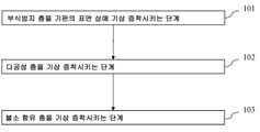
- H—ELECTRICITY
- H10—SEMICONDUCTOR DEVICES; ELECTRIC SOLID-STATE DEVICES NOT OTHERWISE PROVIDED FOR
- H10P—GENERIC PROCESSES OR APPARATUS FOR THE MANUFACTURE OR TREATMENT OF DEVICES COVERED BY CLASS H10
- H10P14/00—Formation of materials, e.g. in the shape of layers or pillars
- H10P14/60—Formation of materials, e.g. in the shape of layers or pillars of insulating materials
- H10P14/66—Formation of materials, e.g. in the shape of layers or pillars of insulating materials characterised by the type of materials
- H10P14/668—Formation of materials, e.g. in the shape of layers or pillars of insulating materials characterised by the type of materials the materials being characterised by the deposition precursor materials
- H10P14/6681—Formation of materials, e.g. in the shape of layers or pillars of insulating materials characterised by the type of materials the materials being characterised by the deposition precursor materials the precursor containing a compound comprising Si
- H10P14/6684—Formation of materials, e.g. in the shape of layers or pillars of insulating materials characterised by the type of materials the materials being characterised by the deposition precursor materials the precursor containing a compound comprising Si the compound comprising silicon and oxygen
- H10P14/6686—Formation of materials, e.g. in the shape of layers or pillars of insulating materials characterised by the type of materials the materials being characterised by the deposition precursor materials the precursor containing a compound comprising Si the compound comprising silicon and oxygen the compound being a molecule comprising at least one silicon-oxygen bond and the compound having hydrogen or an organic group attached to the silicon or oxygen, e.g. a siloxane
-
- H—ELECTRICITY
- H10—SEMICONDUCTOR DEVICES; ELECTRIC SOLID-STATE DEVICES NOT OTHERWISE PROVIDED FOR
- H10W—GENERIC PACKAGES, INTERCONNECTIONS, CONNECTORS OR OTHER CONSTRUCTIONAL DETAILS OF DEVICES COVERED BY CLASS H10
- H10W20/00—Interconnections in chips, wafers or substrates
- H10W20/40—Interconnections external to wafers or substrates, e.g. back-end-of-line [BEOL] metallisations or vias connecting to gate electrodes
- H10W20/45—Interconnections external to wafers or substrates, e.g. back-end-of-line [BEOL] metallisations or vias connecting to gate electrodes characterised by their insulating parts
- H10W20/47—Interconnections external to wafers or substrates, e.g. back-end-of-line [BEOL] metallisations or vias connecting to gate electrodes characterised by their insulating parts comprising two or more dielectric layers having different properties, e.g. different dielectric constants
-
- H—ELECTRICITY
- H10—SEMICONDUCTOR DEVICES; ELECTRIC SOLID-STATE DEVICES NOT OTHERWISE PROVIDED FOR
- H10W—GENERIC PACKAGES, INTERCONNECTIONS, CONNECTORS OR OTHER CONSTRUCTIONAL DETAILS OF DEVICES COVERED BY CLASS H10
- H10W20/00—Interconnections in chips, wafers or substrates
- H10W20/40—Interconnections external to wafers or substrates, e.g. back-end-of-line [BEOL] metallisations or vias connecting to gate electrodes
- H10W20/45—Interconnections external to wafers or substrates, e.g. back-end-of-line [BEOL] metallisations or vias connecting to gate electrodes characterised by their insulating parts
- H10W20/48—Insulating materials thereof
-
- H—ELECTRICITY
- H10—SEMICONDUCTOR DEVICES; ELECTRIC SOLID-STATE DEVICES NOT OTHERWISE PROVIDED FOR
- H10W—GENERIC PACKAGES, INTERCONNECTIONS, CONNECTORS OR OTHER CONSTRUCTIONAL DETAILS OF DEVICES COVERED BY CLASS H10
- H10W70/00—Package substrates; Interposers; Redistribution layers [RDL]
- H10W70/01—Manufacture or treatment
- H10W70/05—Manufacture or treatment of insulating or insulated package substrates, or of interposers, or of redistribution layers
-
- B—PERFORMING OPERATIONS; TRANSPORTING
- B05—SPRAYING OR ATOMISING IN GENERAL; APPLYING FLUENT MATERIALS TO SURFACES, IN GENERAL
- B05D—PROCESSES FOR APPLYING FLUENT MATERIALS TO SURFACES, IN GENERAL
- B05D2504/00—Epoxy polymers
-
- B—PERFORMING OPERATIONS; TRANSPORTING
- B05—SPRAYING OR ATOMISING IN GENERAL; APPLYING FLUENT MATERIALS TO SURFACES, IN GENERAL
- B05D—PROCESSES FOR APPLYING FLUENT MATERIALS TO SURFACES, IN GENERAL
- B05D2506/00—Halogenated polymers
- B05D2506/10—Fluorinated polymers
-
- B—PERFORMING OPERATIONS; TRANSPORTING
- B05—SPRAYING OR ATOMISING IN GENERAL; APPLYING FLUENT MATERIALS TO SURFACES, IN GENERAL
- B05D—PROCESSES FOR APPLYING FLUENT MATERIALS TO SURFACES, IN GENERAL
- B05D2518/00—Other type of polymers
- B05D2518/10—Silicon-containing polymers
-
- H—ELECTRICITY
- H10—SEMICONDUCTOR DEVICES; ELECTRIC SOLID-STATE DEVICES NOT OTHERWISE PROVIDED FOR
- H10W—GENERIC PACKAGES, INTERCONNECTIONS, CONNECTORS OR OTHER CONSTRUCTIONAL DETAILS OF DEVICES COVERED BY CLASS H10
- H10W20/00—Interconnections in chips, wafers or substrates
- H10W20/01—Manufacture or treatment
- H10W20/071—Manufacture or treatment of dielectric parts thereof
- H10W20/072—Manufacture or treatment of dielectric parts thereof of dielectric parts comprising air gaps
-
- H—ELECTRICITY
- H10—SEMICONDUCTOR DEVICES; ELECTRIC SOLID-STATE DEVICES NOT OTHERWISE PROVIDED FOR
- H10W—GENERIC PACKAGES, INTERCONNECTIONS, CONNECTORS OR OTHER CONSTRUCTIONAL DETAILS OF DEVICES COVERED BY CLASS H10
- H10W20/00—Interconnections in chips, wafers or substrates
- H10W20/40—Interconnections external to wafers or substrates, e.g. back-end-of-line [BEOL] metallisations or vias connecting to gate electrodes
- H10W20/45—Interconnections external to wafers or substrates, e.g. back-end-of-line [BEOL] metallisations or vias connecting to gate electrodes characterised by their insulating parts
- H10W20/46—Interconnections external to wafers or substrates, e.g. back-end-of-line [BEOL] metallisations or vias connecting to gate electrodes characterised by their insulating parts comprising air gaps
Landscapes
- Chemical & Material Sciences (AREA)
- Engineering & Computer Science (AREA)
- Organic Chemistry (AREA)
- Chemical Kinetics & Catalysis (AREA)
- Materials Engineering (AREA)
- Mechanical Engineering (AREA)
- Metallurgy (AREA)
- General Chemical & Material Sciences (AREA)
- Physics & Mathematics (AREA)
- Plasma & Fusion (AREA)
- Inorganic Chemistry (AREA)
- Manufacturing & Machinery (AREA)
- Microelectronics & Electronic Packaging (AREA)
- Formation Of Insulating Films (AREA)
- Internal Circuitry In Semiconductor Integrated Circuit Devices (AREA)
- Chemical Vapour Deposition (AREA)
- Ceramic Engineering (AREA)
Applications Claiming Priority (3)
| Application Number | Priority Date | Filing Date | Title |
|---|---|---|---|
| CN201910413247.9A CN110158052B (zh) | 2019-05-17 | 2019-05-17 | 低介电常数膜及其制备方法 |
| CN201910413247.9 | 2019-05-17 | ||
| PCT/CN2020/090119 WO2020233480A1 (zh) | 2019-05-17 | 2020-05-14 | 低介电常数膜及其制备方法 |
Publications (1)
| Publication Number | Publication Date |
|---|---|
| KR20220008319A true KR20220008319A (ko) | 2022-01-20 |
Family
ID=67631273
Family Applications (1)
| Application Number | Title | Priority Date | Filing Date |
|---|---|---|---|
| KR1020217040802A Abandoned KR20220008319A (ko) | 2019-05-17 | 2020-05-14 | 저유전율 필름 및 이의 제조 방법 |
Country Status (7)
| Country | Link |
|---|---|
| US (1) | US11904352B2 (https=) |
| EP (1) | EP3971320A4 (https=) |
| JP (1) | JP7475371B2 (https=) |
| KR (1) | KR20220008319A (https=) |
| CN (1) | CN110158052B (https=) |
| TW (1) | TWI743790B (https=) |
| WO (1) | WO2020233480A1 (https=) |
Families Citing this family (6)
| Publication number | Priority date | Publication date | Assignee | Title |
|---|---|---|---|---|
| CN110129769B (zh) | 2019-05-17 | 2021-05-14 | 江苏菲沃泰纳米科技股份有限公司 | 疏水性的低介电常数膜及其制备方法 |
| CN110158052B (zh) | 2019-05-17 | 2021-05-14 | 江苏菲沃泰纳米科技股份有限公司 | 低介电常数膜及其制备方法 |
| US11898248B2 (en) * | 2019-12-18 | 2024-02-13 | Jiangsu Favored Nanotechnology Co., Ltd. | Coating apparatus and coating method |
| CN115400930A (zh) * | 2021-05-26 | 2022-11-29 | 江苏菲沃泰纳米科技股份有限公司 | 一种等离子体聚合涂层、制备方法及器件 |
| KR102846208B1 (ko) * | 2022-01-20 | 2025-08-19 | 성균관대학교산학협력단 | 플라즈마 중합체 박막 및 이의 제조 방법 |
| CN114438478B (zh) * | 2022-01-27 | 2024-04-26 | 深圳市技高美纳米科技有限公司 | 硅基纳米涂层的制备方法、硅基纳米涂层和印制电路板组件 |
Family Cites Families (42)
| Publication number | Priority date | Publication date | Assignee | Title |
|---|---|---|---|---|
| US5244730A (en) | 1991-04-30 | 1993-09-14 | International Business Machines Corporation | Plasma deposition of fluorocarbon |
| JP3435186B2 (ja) | 1993-04-15 | 2003-08-11 | 株式会社東芝 | 半導体装置 |
| US6149987A (en) * | 1998-04-07 | 2000-11-21 | Applied Materials, Inc. | Method for depositing low dielectric constant oxide films |
| US6458718B1 (en) | 2000-04-28 | 2002-10-01 | Asm Japan K.K. | Fluorine-containing materials and processes |
| JP3545364B2 (ja) * | 2000-12-19 | 2004-07-21 | キヤノン販売株式会社 | 半導体装置及びその製造方法 |
| SG98468A1 (en) | 2001-01-17 | 2003-09-19 | Air Prod & Chem | Organosilicon precursors for interlayer dielectric films with low dielectric constants |
| US6716770B2 (en) * | 2001-05-23 | 2004-04-06 | Air Products And Chemicals, Inc. | Low dielectric constant material and method of processing by CVD |
| KR20030002993A (ko) | 2001-06-29 | 2003-01-09 | 학교법인 포항공과대학교 | 저유전체 박막의 제조방법 |
| JP3778045B2 (ja) | 2001-10-09 | 2006-05-24 | 三菱電機株式会社 | 低誘電率材料の製造方法および低誘電率材料、並びにこの低誘電率材料を用いた絶縁膜および半導体装置 |
| US7423166B2 (en) * | 2001-12-13 | 2008-09-09 | Advanced Technology Materials, Inc. | Stabilized cyclosiloxanes for use as CVD precursors for low-dielectric constant thin films |
| EP1504138A2 (en) * | 2002-05-08 | 2005-02-09 | Applied Materials, Inc. | Method for using low dielectric constant film by electron beam |
| US20040137757A1 (en) * | 2003-01-13 | 2004-07-15 | Applied Materials, Inc. | Method and apparatus to improve cracking thresholds and mechanical properties of low-k dielectric material |
| US7288292B2 (en) | 2003-03-18 | 2007-10-30 | International Business Machines Corporation | Ultra low k (ULK) SiCOH film and method |
| US20040197474A1 (en) | 2003-04-01 | 2004-10-07 | Vrtis Raymond Nicholas | Method for enhancing deposition rate of chemical vapor deposition films |
| JP4344841B2 (ja) | 2003-05-30 | 2009-10-14 | 独立行政法人産業技術総合研究所 | 低誘電率絶縁膜の形成方法 |
| US7646081B2 (en) | 2003-07-08 | 2010-01-12 | Silecs Oy | Low-K dielectric material |
| US7030468B2 (en) | 2004-01-16 | 2006-04-18 | International Business Machines Corporation | Low k and ultra low k SiCOH dielectric films and methods to form the same |
| US7049247B2 (en) | 2004-05-03 | 2006-05-23 | International Business Machines Corporation | Method for fabricating an ultralow dielectric constant material as an intralevel or interlevel dielectric in a semiconductor device and electronic device made |
| US7422776B2 (en) * | 2004-08-24 | 2008-09-09 | Applied Materials, Inc. | Low temperature process to produce low-K dielectrics with low stress by plasma-enhanced chemical vapor deposition (PECVD) |
| US7135402B2 (en) | 2005-02-01 | 2006-11-14 | Taiwan Semiconductor Manufacturing Company, Ltd. | Sealing pores of low-k dielectrics using CxHy |
| JP5093479B2 (ja) * | 2005-11-24 | 2012-12-12 | 日本電気株式会社 | 多孔質絶縁膜の形成方法 |
| US20070172666A1 (en) | 2006-01-24 | 2007-07-26 | Denes Ferencz S | RF plasma-enhanced deposition of fluorinated films |
| CN101393865B (zh) * | 2007-09-17 | 2010-10-13 | 联华电子股份有限公司 | 超低介电常数介电层及其形成方法 |
| TWI510665B (zh) | 2009-02-17 | 2015-12-01 | 東京威力科創股份有限公司 | 使用電漿反應製程來形成氟碳化物層的方法 |
| JP2013520841A (ja) * | 2010-02-25 | 2013-06-06 | アプライド マテリアルズ インコーポレイテッド | プラズマ化学気相堆積による、有機官能基と共にシリコンを含有するハイブリッド前駆体を使用する超低誘電材料 |
| US8178439B2 (en) | 2010-03-30 | 2012-05-15 | Tokyo Electron Limited | Surface cleaning and selective deposition of metal-containing cap layers for semiconductor devices |
| US8216861B1 (en) | 2011-06-28 | 2012-07-10 | Applied Materials, Inc. | Dielectric recovery of plasma damaged low-k films by UV-assisted photochemical deposition |
| WO2013102011A2 (en) | 2011-12-30 | 2013-07-04 | Gvd Corporation | Coatings for electrowetting and electrofluidic devices |
| TWI449802B (zh) | 2012-06-06 | 2014-08-21 | Univ Nat Chiao Tung | 掺碳氮化矽薄膜及其製造方法與裝置 |
| US9352891B2 (en) * | 2012-12-28 | 2016-05-31 | Ade, Inc. | Suspension packaging structures and methods of making and using the same |
| US20140183087A1 (en) * | 2012-12-31 | 2014-07-03 | Funai Electric Co., Ltd. | Fluid Level Sensing Tank Materials |
| GB201305500D0 (en) | 2013-03-26 | 2013-05-08 | Semblant Ltd | Coated electrical assembly |
| US9607825B2 (en) | 2014-04-08 | 2017-03-28 | International Business Machines Corporation | Hydrogen-free silicon-based deposited dielectric films for nano device fabrication |
| KR20160029985A (ko) | 2014-09-05 | 2016-03-16 | 성균관대학교산학협력단 | 유전체에 균일하게 플라즈마를 발생시키는 방법 |
| CN105280816A (zh) | 2015-09-22 | 2016-01-27 | 复旦大学 | 一种使用等离子体交联技术制备有机场效应晶体管介电层的方法 |
| CN106291911B (zh) | 2016-08-10 | 2019-06-11 | 华南师范大学 | 复合层结构的疏水性介电层、其制备方法和电润湿器件 |
| CN106496529B (zh) | 2016-11-17 | 2019-01-18 | 北京航空航天大学 | 一种低介电常数二乙炔基聚合物、其制备方法及其用途 |
| CN106958012A (zh) | 2017-05-21 | 2017-07-18 | 无锡荣坚五金工具有限公司 | 一种基材运动式等离子体放电制备纳米涂层的设备及方法 |
| CN107587120B (zh) | 2017-08-23 | 2018-12-18 | 江苏菲沃泰纳米科技有限公司 | 一种具有调制结构的高绝缘纳米防护涂层的制备方法 |
| CN109277269B (zh) | 2018-10-24 | 2020-07-14 | 江苏菲沃泰纳米科技有限公司 | 一种环氧纳米涂层及其制备方法 |
| CN110129769B (zh) | 2019-05-17 | 2021-05-14 | 江苏菲沃泰纳米科技股份有限公司 | 疏水性的低介电常数膜及其制备方法 |
| CN110158052B (zh) * | 2019-05-17 | 2021-05-14 | 江苏菲沃泰纳米科技股份有限公司 | 低介电常数膜及其制备方法 |
-
2019
- 2019-05-17 CN CN201910413247.9A patent/CN110158052B/zh active Active
-
2020
- 2020-05-14 JP JP2021568365A patent/JP7475371B2/ja active Active
- 2020-05-14 US US17/595,436 patent/US11904352B2/en active Active
- 2020-05-14 EP EP20809129.8A patent/EP3971320A4/en active Pending
- 2020-05-14 WO PCT/CN2020/090119 patent/WO2020233480A1/zh not_active Ceased
- 2020-05-14 KR KR1020217040802A patent/KR20220008319A/ko not_active Abandoned
- 2020-05-18 TW TW109116440A patent/TWI743790B/zh active
Also Published As
| Publication number | Publication date |
|---|---|
| TWI743790B (zh) | 2021-10-21 |
| US11904352B2 (en) | 2024-02-20 |
| CN110158052B (zh) | 2021-05-14 |
| EP3971320A1 (en) | 2022-03-23 |
| JP7475371B2 (ja) | 2024-04-26 |
| CN110158052A (zh) | 2019-08-23 |
| TW202043541A (zh) | 2020-12-01 |
| JP2022532755A (ja) | 2022-07-19 |
| US20220314271A1 (en) | 2022-10-06 |
| EP3971320A4 (en) | 2023-11-15 |
| WO2020233480A1 (zh) | 2020-11-26 |
Similar Documents
| Publication | Publication Date | Title |
|---|---|---|
| US11904352B2 (en) | Low dielectric constant film and preparation method thereof | |
| JP3881282B2 (ja) | 低誘電率材料およびcvdによる処理方法 | |
| KR100602469B1 (ko) | 저 유전 필름을 위한 기계적 강화제 첨가제 | |
| US6440876B1 (en) | Low-K dielectric constant CVD precursors formed of cyclic siloxanes having in-ring SI—O—C, and uses thereof | |
| JP3930840B2 (ja) | 低κ誘電性無機/有機ハイブリッドフィルム | |
| JP5270442B2 (ja) | ポロゲン、ポロゲン化前駆体、および低誘電定数を有する多孔性有機シリカガラスフィルムを得るためにそれらを用いる方法 | |
| TW200307761A (en) | Porogens, porogenated precursors and methods for using the same to provide porous organosilica glass films with low dielectric constants | |
| US20110206857A1 (en) | Ultra low dielectric materials using hybrid precursors containing silicon with organic functional groups by plasma-enhanced chemical vapor deposition | |
| CN109722648B (zh) | 硅杂环状化合物和使用其沉积含硅膜的方法 | |
| JP2004312041A5 (https=) | ||
| TWI676632B (zh) | 烷氧基矽環狀或醯氧基矽環狀化合物及使用其沉積薄膜的方法 | |
| CN101743247A (zh) | 利用等离子体增强化学气相沉积来制造高机械性能的极低k膜的新型硅前驱物 | |
| JP2004190033A (ja) | 低誘電率材料及びcvdによる処理方法 | |
| TW202012419A (zh) | 矽化合物及使用其沉積膜的方法 | |
| EP2163664A1 (en) | Method for depositing si-containing film, insulator film, and semiconductor device | |
| JP2021025124A (ja) | ケイ素化合物及びケイ素化合物を使用してフィルムを堆積する方法 | |
| CN110952074B (zh) | 硅化合物和使用硅化合物沉积膜的方法 |
Legal Events
| Date | Code | Title | Description |
|---|---|---|---|
| A201 | Request for examination | ||
| E13-X000 | Pre-grant limitation requested |
St.27 status event code: A-2-3-E10-E13-lim-X000 |
|
| P11-X000 | Amendment of application requested |
St.27 status event code: A-2-2-P10-P11-nap-X000 |
|
| P13-X000 | Application amended |
St.27 status event code: A-2-2-P10-P13-nap-X000 |
|
| PA0105 | International application |
St.27 status event code: A-0-1-A10-A15-nap-PA0105 |
|
| PA0201 | Request for examination |
St.27 status event code: A-1-2-D10-D11-exm-PA0201 |
|
| PG1501 | Laying open of application |
St.27 status event code: A-1-1-Q10-Q12-nap-PG1501 |
|
| D13-X000 | Search requested |
St.27 status event code: A-1-2-D10-D13-srh-X000 |
|
| D14-X000 | Search report completed |
St.27 status event code: A-1-2-D10-D14-srh-X000 |
|
| E902 | Notification of reason for refusal | ||
| PE0902 | Notice of grounds for rejection |
St.27 status event code: A-1-2-D10-D21-exm-PE0902 |
|
| E13-X000 | Pre-grant limitation requested |
St.27 status event code: A-2-3-E10-E13-lim-X000 |
|
| P11-X000 | Amendment of application requested |
St.27 status event code: A-2-2-P10-P11-nap-X000 |
|
| P13-X000 | Application amended |
St.27 status event code: A-2-2-P10-P13-nap-X000 |
|
| PE0701 | Decision of registration |
St.27 status event code: A-1-2-D10-D22-exm-PE0701 |
|
| R18-X000 | Changes to party contact information recorded |
St.27 status event code: A-3-3-R10-R18-oth-X000 |
|
| PC1904 | Unpaid initial registration fee |
St.27 status event code: A-2-2-U10-U14-oth-PC1904 St.27 status event code: N-2-6-B10-B12-nap-PC1904 |
|
| P22-X000 | Classification modified |
St.27 status event code: A-2-2-P10-P22-nap-X000 |