KR20180098501A - 유기 발광 소자 및 이의 제조방법 - Google Patents
유기 발광 소자 및 이의 제조방법 Download PDFInfo
- Publication number
- KR20180098501A KR20180098501A KR1020180099094A KR20180099094A KR20180098501A KR 20180098501 A KR20180098501 A KR 20180098501A KR 1020180099094 A KR1020180099094 A KR 1020180099094A KR 20180099094 A KR20180099094 A KR 20180099094A KR 20180098501 A KR20180098501 A KR 20180098501A
- Authority
- KR
- South Korea
- Prior art keywords
- light emitting
- organic light
- substrate
- metal pattern
- circuit board
- Prior art date
- Legal status (The legal status is an assumption and is not a legal conclusion. Google has not performed a legal analysis and makes no representation as to the accuracy of the status listed.)
- Granted
Links
Images


Classifications
-
- H—ELECTRICITY
- H10—SEMICONDUCTOR DEVICES; ELECTRIC SOLID-STATE DEVICES NOT OTHERWISE PROVIDED FOR
- H10K—ORGANIC ELECTRIC SOLID-STATE DEVICES
- H10K50/00—Organic light-emitting devices
- H10K50/80—Constructional details
- H10K50/84—Passivation; Containers; Encapsulations
- H10K50/842—Containers
- H10K50/8426—Peripheral sealing arrangements, e.g. adhesives, sealants
-
- H01L51/5246—
-
- H—ELECTRICITY
- H10—SEMICONDUCTOR DEVICES; ELECTRIC SOLID-STATE DEVICES NOT OTHERWISE PROVIDED FOR
- H10K—ORGANIC ELECTRIC SOLID-STATE DEVICES
- H10K59/00—Integrated devices, or assemblies of multiple devices, comprising at least one organic light-emitting element covered by group H10K50/00
- H10K59/80—Constructional details
- H10K59/805—Electrodes
-
- H01L21/3213—
-
- H01L21/76838—
-
- H01L51/0097—
-
- H01L51/5012—
-
- H01L51/5268—
-
- H01L51/56—
-
- H—ELECTRICITY
- H05—ELECTRIC TECHNIQUES NOT OTHERWISE PROVIDED FOR
- H05K—PRINTED CIRCUITS; CASINGS OR CONSTRUCTIONAL DETAILS OF ELECTRIC APPARATUS; MANUFACTURE OF ASSEMBLAGES OF ELECTRICAL COMPONENTS
- H05K1/00—Printed circuits
- H05K1/02—Details
- H05K1/0277—Bendability or stretchability details
- H05K1/028—Bending or folding regions of flexible printed circuits
-
- H—ELECTRICITY
- H05—ELECTRIC TECHNIQUES NOT OTHERWISE PROVIDED FOR
- H05K—PRINTED CIRCUITS; CASINGS OR CONSTRUCTIONAL DETAILS OF ELECTRIC APPARATUS; MANUFACTURE OF ASSEMBLAGES OF ELECTRICAL COMPONENTS
- H05K1/00—Printed circuits
- H05K1/02—Details
- H05K1/0296—Conductive pattern lay-out details not covered by sub groups H05K1/02 - H05K1/0295
- H05K1/0298—Multilayer circuits
-
- H—ELECTRICITY
- H05—ELECTRIC TECHNIQUES NOT OTHERWISE PROVIDED FOR
- H05K—PRINTED CIRCUITS; CASINGS OR CONSTRUCTIONAL DETAILS OF ELECTRIC APPARATUS; MANUFACTURE OF ASSEMBLAGES OF ELECTRICAL COMPONENTS
- H05K1/00—Printed circuits
- H05K1/02—Details
- H05K1/03—Use of materials for the substrate
- H05K1/0313—Organic insulating material
- H05K1/032—Organic insulating material consisting of one material
- H05K1/0346—Organic insulating material consisting of one material containing N
-
- H—ELECTRICITY
- H05—ELECTRIC TECHNIQUES NOT OTHERWISE PROVIDED FOR
- H05K—PRINTED CIRCUITS; CASINGS OR CONSTRUCTIONAL DETAILS OF ELECTRIC APPARATUS; MANUFACTURE OF ASSEMBLAGES OF ELECTRICAL COMPONENTS
- H05K1/00—Printed circuits
- H05K1/02—Details
- H05K1/09—Use of materials for the conductive, e.g. metallic pattern
-
- H—ELECTRICITY
- H05—ELECTRIC TECHNIQUES NOT OTHERWISE PROVIDED FOR
- H05K—PRINTED CIRCUITS; CASINGS OR CONSTRUCTIONAL DETAILS OF ELECTRIC APPARATUS; MANUFACTURE OF ASSEMBLAGES OF ELECTRICAL COMPONENTS
- H05K1/00—Printed circuits
- H05K1/18—Printed circuits structurally associated with non-printed electric components
- H05K1/181—Printed circuits structurally associated with non-printed electric components associated with surface mounted components
-
- H—ELECTRICITY
- H10—SEMICONDUCTOR DEVICES; ELECTRIC SOLID-STATE DEVICES NOT OTHERWISE PROVIDED FOR
- H10K—ORGANIC ELECTRIC SOLID-STATE DEVICES
- H10K50/00—Organic light-emitting devices
- H10K50/10—OLEDs or polymer light-emitting diodes [PLED]
- H10K50/11—OLEDs or polymer light-emitting diodes [PLED] characterised by the electroluminescent [EL] layers
-
- H—ELECTRICITY
- H10—SEMICONDUCTOR DEVICES; ELECTRIC SOLID-STATE DEVICES NOT OTHERWISE PROVIDED FOR
- H10K—ORGANIC ELECTRIC SOLID-STATE DEVICES
- H10K50/00—Organic light-emitting devices
- H10K50/80—Constructional details
- H10K50/805—Electrodes
-
- H—ELECTRICITY
- H10—SEMICONDUCTOR DEVICES; ELECTRIC SOLID-STATE DEVICES NOT OTHERWISE PROVIDED FOR
- H10K—ORGANIC ELECTRIC SOLID-STATE DEVICES
- H10K50/00—Organic light-emitting devices
- H10K50/80—Constructional details
- H10K50/84—Passivation; Containers; Encapsulations
- H10K50/841—Self-supporting sealing arrangements
-
- H—ELECTRICITY
- H10—SEMICONDUCTOR DEVICES; ELECTRIC SOLID-STATE DEVICES NOT OTHERWISE PROVIDED FOR
- H10K—ORGANIC ELECTRIC SOLID-STATE DEVICES
- H10K50/00—Organic light-emitting devices
- H10K50/80—Constructional details
- H10K50/84—Passivation; Containers; Encapsulations
- H10K50/846—Passivation; Containers; Encapsulations comprising getter material or desiccants
-
- H—ELECTRICITY
- H10—SEMICONDUCTOR DEVICES; ELECTRIC SOLID-STATE DEVICES NOT OTHERWISE PROVIDED FOR
- H10K—ORGANIC ELECTRIC SOLID-STATE DEVICES
- H10K50/00—Organic light-emitting devices
- H10K50/80—Constructional details
- H10K50/85—Arrangements for extracting light from the devices
- H10K50/854—Arrangements for extracting light from the devices comprising scattering means
-
- H—ELECTRICITY
- H10—SEMICONDUCTOR DEVICES; ELECTRIC SOLID-STATE DEVICES NOT OTHERWISE PROVIDED FOR
- H10K—ORGANIC ELECTRIC SOLID-STATE DEVICES
- H10K59/00—Integrated devices, or assemblies of multiple devices, comprising at least one organic light-emitting element covered by group H10K50/00
- H10K59/10—OLED displays
- H10K59/12—Active-matrix OLED [AMOLED] displays
- H10K59/131—Interconnections, e.g. wiring lines or terminals
-
- H—ELECTRICITY
- H10—SEMICONDUCTOR DEVICES; ELECTRIC SOLID-STATE DEVICES NOT OTHERWISE PROVIDED FOR
- H10K—ORGANIC ELECTRIC SOLID-STATE DEVICES
- H10K59/00—Integrated devices, or assemblies of multiple devices, comprising at least one organic light-emitting element covered by group H10K50/00
- H10K59/80—Constructional details
- H10K59/87—Passivation; Containers; Encapsulations
- H10K59/871—Self-supporting sealing arrangements
-
- H—ELECTRICITY
- H10—SEMICONDUCTOR DEVICES; ELECTRIC SOLID-STATE DEVICES NOT OTHERWISE PROVIDED FOR
- H10K—ORGANIC ELECTRIC SOLID-STATE DEVICES
- H10K71/00—Manufacture or treatment specially adapted for the organic devices covered by this subclass
-
- H—ELECTRICITY
- H10—SEMICONDUCTOR DEVICES; ELECTRIC SOLID-STATE DEVICES NOT OTHERWISE PROVIDED FOR
- H10K—ORGANIC ELECTRIC SOLID-STATE DEVICES
- H10K71/00—Manufacture or treatment specially adapted for the organic devices covered by this subclass
- H10K71/50—Forming devices by joining two substrates together, e.g. lamination techniques
-
- H—ELECTRICITY
- H10—SEMICONDUCTOR DEVICES; ELECTRIC SOLID-STATE DEVICES NOT OTHERWISE PROVIDED FOR
- H10K—ORGANIC ELECTRIC SOLID-STATE DEVICES
- H10K77/00—Constructional details of devices covered by this subclass and not covered by groups H10K10/80, H10K30/80, H10K50/80 or H10K59/80
- H10K77/10—Substrates, e.g. flexible substrates
- H10K77/111—Flexible substrates
-
- H—ELECTRICITY
- H10—SEMICONDUCTOR DEVICES; ELECTRIC SOLID-STATE DEVICES NOT OTHERWISE PROVIDED FOR
- H10P—GENERIC PROCESSES OR APPARATUS FOR THE MANUFACTURE OR TREATMENT OF DEVICES COVERED BY CLASS H10
- H10P50/00—Etching of wafers, substrates or parts of devices
-
- H—ELECTRICITY
- H10—SEMICONDUCTOR DEVICES; ELECTRIC SOLID-STATE DEVICES NOT OTHERWISE PROVIDED FOR
- H10W—GENERIC PACKAGES, INTERCONNECTIONS, CONNECTORS OR OTHER CONSTRUCTIONAL DETAILS OF DEVICES COVERED BY CLASS H10
- H10W20/00—Interconnections in chips, wafers or substrates
- H10W20/01—Manufacture or treatment
- H10W20/031—Manufacture or treatment of conductive parts of the interconnections
-
- F—MECHANICAL ENGINEERING; LIGHTING; HEATING; WEAPONS; BLASTING
- F21—LIGHTING
- F21Y—INDEXING SCHEME ASSOCIATED WITH SUBCLASSES F21K, F21L, F21S and F21V, RELATING TO THE FORM OR THE KIND OF THE LIGHT SOURCES OR OF THE COLOUR OF THE LIGHT EMITTED
- F21Y2105/00—Planar light sources
-
- F—MECHANICAL ENGINEERING; LIGHTING; HEATING; WEAPONS; BLASTING
- F21—LIGHTING
- F21Y—INDEXING SCHEME ASSOCIATED WITH SUBCLASSES F21K, F21L, F21S and F21V, RELATING TO THE FORM OR THE KIND OF THE LIGHT SOURCES OR OF THE COLOUR OF THE LIGHT EMITTED
- F21Y2115/00—Light-generating elements of semiconductor light sources
- F21Y2115/10—Light-emitting diodes [LED]
- F21Y2115/15—Organic light-emitting diodes [OLED]
-
- H01L2227/32—
-
- H01L2924/12044—
-
- H—ELECTRICITY
- H05—ELECTRIC TECHNIQUES NOT OTHERWISE PROVIDED FOR
- H05K—PRINTED CIRCUITS; CASINGS OR CONSTRUCTIONAL DETAILS OF ELECTRIC APPARATUS; MANUFACTURE OF ASSEMBLAGES OF ELECTRICAL COMPONENTS
- H05K2201/00—Indexing scheme relating to printed circuits covered by H05K1/00
- H05K2201/10—Details of components or other objects attached to or integrated in a printed circuit board
- H05K2201/10007—Types of components
- H05K2201/10106—Light emitting diode [LED]
-
- H—ELECTRICITY
- H10—SEMICONDUCTOR DEVICES; ELECTRIC SOLID-STATE DEVICES NOT OTHERWISE PROVIDED FOR
- H10K—ORGANIC ELECTRIC SOLID-STATE DEVICES
- H10K2102/00—Constructional details relating to the organic devices covered by this subclass
- H10K2102/301—Details of OLEDs
- H10K2102/311—Flexible OLED
-
- H—ELECTRICITY
- H10—SEMICONDUCTOR DEVICES; ELECTRIC SOLID-STATE DEVICES NOT OTHERWISE PROVIDED FOR
- H10K—ORGANIC ELECTRIC SOLID-STATE DEVICES
- H10K2102/00—Constructional details relating to the organic devices covered by this subclass
- H10K2102/301—Details of OLEDs
- H10K2102/351—Thickness
-
- H—ELECTRICITY
- H10—SEMICONDUCTOR DEVICES; ELECTRIC SOLID-STATE DEVICES NOT OTHERWISE PROVIDED FOR
- H10K—ORGANIC ELECTRIC SOLID-STATE DEVICES
- H10K59/00—Integrated devices, or assemblies of multiple devices, comprising at least one organic light-emitting element covered by group H10K50/00
- H10K59/10—OLED displays
- H10K59/12—Active-matrix OLED [AMOLED] displays
- H10K59/1201—Manufacture or treatment
-
- H—ELECTRICITY
- H10—SEMICONDUCTOR DEVICES; ELECTRIC SOLID-STATE DEVICES NOT OTHERWISE PROVIDED FOR
- H10K—ORGANIC ELECTRIC SOLID-STATE DEVICES
- H10K59/00—Integrated devices, or assemblies of multiple devices, comprising at least one organic light-emitting element covered by group H10K50/00
- H10K59/80—Constructional details
- H10K59/87—Passivation; Containers; Encapsulations
- H10K59/871—Self-supporting sealing arrangements
- H10K59/8722—Peripheral sealing arrangements, e.g. adhesives, sealants
-
- H—ELECTRICITY
- H10—SEMICONDUCTOR DEVICES; ELECTRIC SOLID-STATE DEVICES NOT OTHERWISE PROVIDED FOR
- H10K—ORGANIC ELECTRIC SOLID-STATE DEVICES
- H10K59/00—Integrated devices, or assemblies of multiple devices, comprising at least one organic light-emitting element covered by group H10K50/00
- H10K59/80—Constructional details
- H10K59/87—Passivation; Containers; Encapsulations
- H10K59/874—Passivation; Containers; Encapsulations including getter material or desiccant
-
- H—ELECTRICITY
- H10—SEMICONDUCTOR DEVICES; ELECTRIC SOLID-STATE DEVICES NOT OTHERWISE PROVIDED FOR
- H10K—ORGANIC ELECTRIC SOLID-STATE DEVICES
- H10K59/00—Integrated devices, or assemblies of multiple devices, comprising at least one organic light-emitting element covered by group H10K50/00
- H10K59/80—Constructional details
- H10K59/875—Arrangements for extracting light from the devices
- H10K59/877—Arrangements for extracting light from the devices comprising scattering means
-
- Y—GENERAL TAGGING OF NEW TECHNOLOGICAL DEVELOPMENTS; GENERAL TAGGING OF CROSS-SECTIONAL TECHNOLOGIES SPANNING OVER SEVERAL SECTIONS OF THE IPC; TECHNICAL SUBJECTS COVERED BY FORMER USPC CROSS-REFERENCE ART COLLECTIONS [XRACs] AND DIGESTS
- Y02—TECHNOLOGIES OR APPLICATIONS FOR MITIGATION OR ADAPTATION AGAINST CLIMATE CHANGE
- Y02E—REDUCTION OF GREENHOUSE GAS [GHG] EMISSIONS, RELATED TO ENERGY GENERATION, TRANSMISSION OR DISTRIBUTION
- Y02E10/00—Energy generation through renewable energy sources
- Y02E10/50—Photovoltaic [PV] energy
- Y02E10/549—Organic PV cells
Landscapes
- Engineering & Computer Science (AREA)
- Physics & Mathematics (AREA)
- Optics & Photonics (AREA)
- Microelectronics & Electronic Packaging (AREA)
- Manufacturing & Machinery (AREA)
- Electroluminescent Light Sources (AREA)
Abstract
Description
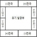
도 2는 본 명세서의 일 실시상태에 따라 유기 발광 소자의 유기 발광부에 연성인쇄회로기판을 적용하는 그림을 나타낸 것이다.
도 3은 본 명세서의 일 실시상태에 따른 유기 발광 소자의 모식도이다.
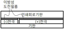
도 4는 본 명세서의 일 실시상태에 따른 유기 발광 소자의 측면도이다.
Claims (33)
- 기판; 상기 기판 상에 제1 전극, 유기물층 및 제2 전극이 순차적으로 적층된 유기 발광부; 및 상기 기판 중 유기 발광부의 외측을 덮는 밀봉부를 포함하고,
상기 밀봉부는, 기재 및 상기 기재의 일면의 가장자리에 형성된 1 종 이상의 금속 패턴, 상기 기재의 일면에 상기 금속 패턴과 전기적으로 연결되지 않고 상기 유기 발광부의 발광 영역의 상부에 구비되는 금속판, 및 상기 기재와 금속 패턴 사이, 2종 이상의 금속 패턴 사이 및 금속 패턴 상부 중 적어도 하나에 구비된 절연층을 포함하는 인쇄회로기판; 및 상기 인쇄회로기판과 상기 유기 발광부의 외측 사이를 채우는 실링층을 포함하는 것인 유기 발광 소자. - 청구항 1에 있어서, 상기 인쇄회로기판은 연성인쇄회로기판인 것인 유기 발광 소자.
- 청구항 1에 있어서, 상기 제1 전극 또는 제2 전극은 상기 금속 패턴을 통하여 외부 전원과 전기적으로 연결되는 것인 유기 발광 소자.
- 청구항 1에 있어서, 상기 금속 패턴은 상기 제1 전극과 외부 전원을 전기적으로 연결하는 제1 금속 패턴을 포함하는 것인 유기 발광 소자.
- 청구항 1에 있어서, 상기 금속 패턴은 상기 제2 전극과 외부 전원을 전기적으로 연결하는 제2 금속 패턴을 포함하는 것인 유기 발광 소자.
- 청구항 1에 있어서, 상기 금속판은 구리, 철, 니켈, 티타늄, 알루미늄, 은 및 금으로 구성되는 군으로부터 선택되는 1종, 또는 2종 이상의 합금; 또는 스테인레스강의 박막인 것인 유기 발광 소자.
- 청구항 1에 있어서, 상기 금속판의 크기는 상기 유기 발광부의 크기에 대응하거나 상기 유기 발광부의 크기보다 더 큰 것인 유기 발광 소자.
- 청구항 1에 있어서, 상기 기재의 일면의 가장자리에 구비된 금속 패턴은 제1금속 패턴 및 제2 금속 패턴을 포함하고,
상기 제1 금속 패턴은 상기 제1 전극과 외부 전원을 전기적으로 연결하며,
상기 제2 금속 패턴은 상기 제2 전극과 외부 전원을 전기적으로 연결하고,
상기 제1 금속 패턴 및 제2 금속 패턴은 각각 이격되어 전기적으로 단락된 구조인 것인 유기 발광 소자. - 청구항 1에 있어서, 상기 밀봉부는 상기 인쇄회로기판과 상기 기판을 접착하는 이방성 도전필름을 더 포함하는 것인 유기 발광 소자.
- 청구항 1에 있어서, 상기 유기 발광 소자는 상기 기재의 타면의 가장자리에 구비된 이방성 도전필름을 더 포함하고,
상기 실링층은 상기 기재의 타면 중 이방성 도전필름이 구비되지 않은 영역에 구비되는 것인 유기 발광 소자. - 청구항 1에 있어서, 상기 절연층의 재질은 폴리이미드계 수지인 것인 유기 발광 소자.
- 청구항 1에 있어서, 상기 금속 패턴은 구리, 철, 니켈, 티타늄, 알루미늄, 은 및 금으로 구성되는 군으로부터 선택되는 1종, 또는 2종 이상의 합금; 또는 스테인레스강의 박막인 것인 유기 발광 소자.
- 청구항 1에 있어서, 상기 기판은 유리 기판 또는 플라스틱 기판인 것인 유기 발광 소자.
- 청구항 1에 있어서, 상기 인쇄회로기판의 두께는 20 내지 200 μm인 것인 유기 발광 소자.
- 청구항 1에 있어서, 상기 실링층의 두께는 10 내지 50 μm인 것인 유기 발광 소자.
- 청구항 1에 있어서, 상기 실링층은 게터(getter)를 포함하는 점착제인 것인유기 발광 소자.
- 청구항 1에 있어서, 상기 유기 발광 소자는 플렉서블 유기 발광 소자인 것인 유기 발광 소자.
- 청구항 1에 있어서, 상기 기판과 상기 제1 전극 사이 및 상기 기판의 상기 제1 전극이 구비되는 면과 대향하는 면 중 적어도 하나에 1 이상의 광산란층을 더 포함하는 것인 유기 발광 소자.
- 청구항 1 내지 18 중 어느 한 항에 따른 유기 발광 소자를 포함하는 디스플 레이 장치.
- 청구항 1 내지 18 중 어느 한 항에 따른 유기 발광 소자를 포함하는 조명 장치.
- 기판 상에 제1 전극, 유기물층 및 제2 전극을 순차적으로 적층하여 유기 발광부를 형성하는 단계; 및
상기 기판 중 유기 발광부의 외측을 덮는 밀봉부를 설치하는 단계를 포함하고,
상기 밀봉부는, 기재 및 상기 기재의 일면의 가장자리에 형성된 1 종 이상의 금속 패턴, 상기 기재의 일면에 상기 금속 패턴과 전기적으로 연결되지 않고 상기 유기 발광부의 발광 영역의 상부에 구비되는 금속판, 및 상기 기재와 금속 패턴 사이, 2종 이상의 금속 패턴 사이 및 금속 패턴 상부 중 적어도 하나에 구비된 절연층을 포함하는 인쇄회로기판; 및 상기 인쇄회로기판과 상기 유기 발광부의 외측 사이를 채우는 실링층을 포함하는 것인 유기 발광 소자의 제조방법. - 청구항 21에 있어서, 상기 인쇄회로기판은 연성인쇄회로기판인 것인 유기 발광 소자의 제조방법.
- 청구항 21에 있어서, 상기 밀봉부를 설치하는 단계에서, 상기 인쇄회로기판과 상기 기판은 이방성 도전필름에 의해서 접착된 것인 유기 발광 소자의 제조방법.
- 청구항 21에 있어서, 상기 금속판은 구리, 철, 니켈, 티타늄, 알루미늄, 은 및 금으로 구성되는 군으로부터 선택되는 1종, 또는 2종 이상의 합금; 또는 스테인레스강의 박막인 것인 유기 발광 소자의 제조방법.
- 기재;
상기 기재의 일면의 가장자리에 구비된 1 종 이상의 금속 패턴;
상기 기재의 일면에 상기 금속 패턴과 전기적으로 연결되지 않고 상기 유기 발광부의 발광 영역의 상부에 구비되는 금속판;
상기 기재와 금속 패턴 사이, 2종 이상의 금속 패턴 사이 및 금속 패턴 상부 중 적어도 하나에 구비된 절연층; 및
상기 기재의 타면에 구비된 실링층을 포함하는 것인 인쇄회로기판의 구조체. - 청구항 25에 있어서, 상기 인쇄회로기판의 구조체는 연성인쇄회로기판의 구조체인 것인 인쇄회로기판의 구조체.
- 청구항 25에 있어서, 상기 금속판은 구리, 철, 니켈, 티타늄, 알루미늄, 은 및 금으로 구성되는 군으로부터 선택되는 1종, 또는 2종 이상의 합금; 또는 스테인레스강의 박막인 것인 인쇄회로기판의 구조체.
- 청구항 25에 있어서, 상기 인쇄회로기판의 구조체는 제1 전극 및 제2 전극이 구비된 소자를 더 포함하고,
상기 금속 패턴은 상기 제1 전극과 외부 전원을 전기적으로 연결하는 제1 금속 패턴 및 상기 제2 전극과 외부 전원을 전기적으로 연결하는 제2 금속 패턴을 포함하는 인쇄회로기판의 구조체. - 청구항 25에 있어서, 상기 절연층의 재질은 폴리이미드계 수지인 것인 인쇄회로기판의 구조체.
- 청구항 25에 있어서, 상기 금속 패턴은 구리, 철, 니켈, 티타늄, 알루미늄, 은 및 금으로 구성되는 군으로부터 선택되는 1종, 또는 2종 이상의 합금; 또는 스테인레스강의 박막인 것인 인쇄회로기판의 구조체.
- 청구항 25에 있어서, 상기 기재의 타면의 가장자리에 구비된 이방성 도전필름을 더 포함하고, 상기 실링층은 상기 기재의 타면 중 이방성 도전필름이 구비되지 않은 영역에 구비되는 것인 인쇄회로기판의 구조체.
- 청구항 25에 있어서, 상기 실링층의 두께는 10 내지 50 μm인 것인 인쇄회로 기판의 구조체.
- 청구항 25에 있어서, 상기 실링층은 게터(getter)를 포함하는 점착제인 것인 인쇄회로기판의 구조체.
Applications Claiming Priority (2)
| Application Number | Priority Date | Filing Date | Title |
|---|---|---|---|
| KR1020130062366 | 2013-05-31 | ||
| KR20130062366 | 2013-05-31 |
Related Parent Applications (1)
| Application Number | Title | Priority Date | Filing Date |
|---|---|---|---|
| KR1020160025171A Division KR20160030913A (ko) | 2013-05-31 | 2016-03-02 | 유기 발광 소자 및 이의 제조방법 |
Publications (2)
| Publication Number | Publication Date |
|---|---|
| KR20180098501A true KR20180098501A (ko) | 2018-09-04 |
| KR101990323B1 KR101990323B1 (ko) | 2019-06-19 |
Family
ID=51989139
Family Applications (3)
| Application Number | Title | Priority Date | Filing Date |
|---|---|---|---|
| KR1020140066496A Ceased KR20140141528A (ko) | 2013-05-31 | 2014-05-30 | 유기 발광 소자 및 이의 제조방법 |
| KR1020160025171A Ceased KR20160030913A (ko) | 2013-05-31 | 2016-03-02 | 유기 발광 소자 및 이의 제조방법 |
| KR1020180099094A Active KR101990323B1 (ko) | 2013-05-31 | 2018-08-24 | 유기 발광 소자 및 이의 제조방법 |
Family Applications Before (2)
| Application Number | Title | Priority Date | Filing Date |
|---|---|---|---|
| KR1020140066496A Ceased KR20140141528A (ko) | 2013-05-31 | 2014-05-30 | 유기 발광 소자 및 이의 제조방법 |
| KR1020160025171A Ceased KR20160030913A (ko) | 2013-05-31 | 2016-03-02 | 유기 발광 소자 및 이의 제조방법 |
Country Status (7)
| Country | Link |
|---|---|
| US (1) | US9806282B2 (ko) |
| EP (1) | EP2993712B1 (ko) |
| JP (1) | JP6452678B2 (ko) |
| KR (3) | KR20140141528A (ko) |
| CN (1) | CN105247698B (ko) |
| TW (1) | TWI604601B (ko) |
| WO (1) | WO2014193196A1 (ko) |
Cited By (1)
| Publication number | Priority date | Publication date | Assignee | Title |
|---|---|---|---|---|
| KR20200123637A (ko) * | 2019-04-22 | 2020-10-30 | 주식회사 오성디스플레이 | 캐비넷이 체결된 디스플레이의 백보드 |
Families Citing this family (3)
| Publication number | Priority date | Publication date | Assignee | Title |
|---|---|---|---|---|
| CN105633281B (zh) * | 2016-01-06 | 2018-07-17 | 京东方科技集团股份有限公司 | 一种柔性显示面板及其封装方法、显示装置 |
| WO2017146477A1 (ko) | 2016-02-26 | 2017-08-31 | 서울반도체주식회사 | 디스플레이 장치 및 그의 제조 방법 |
| WO2021250727A1 (ja) | 2020-06-08 | 2021-12-16 | オリンパス株式会社 | 電子モジュール、電子モジュールの製造方法および内視鏡 |
Citations (4)
| Publication number | Priority date | Publication date | Assignee | Title |
|---|---|---|---|---|
| KR19980071030A (ko) | 1997-02-03 | 1998-10-26 | 가네꼬히사시 | 유기 el 소자 |
| KR20110075684A (ko) * | 2009-12-28 | 2011-07-06 | 삼성모바일디스플레이주식회사 | 유기 발광 조명 장치 |
| KR20120062374A (ko) * | 2010-12-06 | 2012-06-14 | 삼성모바일디스플레이주식회사 | 광 산란 기판, 이의 제조 방법, 이를 포함하는 유기 발광 표시 장치 및 유기 발광 표시 장치의 제조 방법 |
| KR20120068380A (ko) * | 2010-12-17 | 2012-06-27 | 삼성모바일디스플레이주식회사 | 표시 장치 및 유기 발광 표시 장치 |
Family Cites Families (22)
| Publication number | Priority date | Publication date | Assignee | Title |
|---|---|---|---|---|
| JP2003109747A (ja) * | 2001-07-24 | 2003-04-11 | Matsushita Electric Works Ltd | 有機エレクトロルミネッセンス面発光体及び液晶表示装置 |
| US6936131B2 (en) * | 2002-01-31 | 2005-08-30 | 3M Innovative Properties Company | Encapsulation of organic electronic devices using adsorbent loaded adhesives |
| US6965197B2 (en) | 2002-10-01 | 2005-11-15 | Eastman Kodak Company | Organic light-emitting device having enhanced light extraction efficiency |
| JP4526771B2 (ja) * | 2003-03-14 | 2010-08-18 | 株式会社半導体エネルギー研究所 | 半導体装置の作製方法 |
| KR100908230B1 (ko) * | 2003-04-04 | 2009-07-20 | 삼성모바일디스플레이주식회사 | 전계발광소자 |
| US7602118B2 (en) * | 2005-02-24 | 2009-10-13 | Eastman Kodak Company | OLED device having improved light output |
| JP2006261057A (ja) * | 2005-03-18 | 2006-09-28 | Fuji Photo Film Co Ltd | 有機電界発光素子 |
| US7361842B2 (en) * | 2005-06-30 | 2008-04-22 | Intel Corporation | Apparatus and method for an embedded air dielectric for a package and a printed circuit board |
| US20070096631A1 (en) * | 2005-11-01 | 2007-05-03 | Un-Cheol Sung | Flat panel display and fabricating method thereof |
| JP5362948B2 (ja) * | 2006-06-27 | 2013-12-11 | パナソニック株式会社 | 有機エレクトロルミネッセンス発光装置及び有機エレクトロルミネッセンス照明装置 |
| KR100809693B1 (ko) | 2006-08-01 | 2008-03-06 | 삼성전자주식회사 | 하부 반도체 칩에 대한 신뢰도가 개선된 수직 적층형멀티칩 패키지 및 그 제조방법 |
| KR101383711B1 (ko) | 2007-08-08 | 2014-04-09 | 삼성디스플레이 주식회사 | 표시 장치와 이의 제조방법 |
| TWI423718B (zh) * | 2009-10-21 | 2014-01-11 | Au Optronics Corp | 有機電致發光裝置及具有此有機電致發光裝置的電子裝置 |
| KR20110064670A (ko) | 2009-12-08 | 2011-06-15 | 삼성모바일디스플레이주식회사 | 게터 조성물 및 상기 게터 조성물을 포함하는 유기 발광 장치 |
| JP2011192567A (ja) | 2010-03-16 | 2011-09-29 | Rohm Co Ltd | 有機el装置 |
| WO2011136262A1 (ja) | 2010-04-27 | 2011-11-03 | Lumiotec株式会社 | 有機el照明装置 |
| US9035545B2 (en) | 2010-07-07 | 2015-05-19 | Lg Chem, Ltd. | Organic light emitting device comprising encapsulating structure |
| KR101700701B1 (ko) * | 2010-09-24 | 2017-02-14 | 삼성전자 주식회사 | 화상 표시 장치 |
| KR101772142B1 (ko) * | 2010-11-29 | 2017-08-29 | 삼성디스플레이 주식회사 | 유기 발광 표시 장치와 유기 발광 표시 장치용 밀봉 기판의 제조 방법 |
| KR20120066352A (ko) * | 2010-12-14 | 2012-06-22 | 삼성모바일디스플레이주식회사 | 유기 발광 표시 장치 및 이의 제조 방법 |
| KR101259052B1 (ko) | 2011-03-30 | 2013-04-29 | 박재훈 | 방열 반사판을 구비한 발광다이오드 소자용 패키지, 방열 반사판을 구비한 발광다이오드 소자용 패키지 어셈블리 및 그 제조방법 |
| JP2013025961A (ja) * | 2011-07-19 | 2013-02-04 | Pioneer Electronic Corp | 有機elモジュール |
-
2014
- 2014-05-30 US US14/787,687 patent/US9806282B2/en active Active
- 2014-05-30 JP JP2016515283A patent/JP6452678B2/ja active Active
- 2014-05-30 WO PCT/KR2014/004867 patent/WO2014193196A1/ko not_active Ceased
- 2014-05-30 EP EP14804041.3A patent/EP2993712B1/en active Active
- 2014-05-30 CN CN201480031338.1A patent/CN105247698B/zh active Active
- 2014-05-30 KR KR1020140066496A patent/KR20140141528A/ko not_active Ceased
- 2014-06-03 TW TW103119189A patent/TWI604601B/zh active
-
2016
- 2016-03-02 KR KR1020160025171A patent/KR20160030913A/ko not_active Ceased
-
2018
- 2018-08-24 KR KR1020180099094A patent/KR101990323B1/ko active Active
Patent Citations (4)
| Publication number | Priority date | Publication date | Assignee | Title |
|---|---|---|---|---|
| KR19980071030A (ko) | 1997-02-03 | 1998-10-26 | 가네꼬히사시 | 유기 el 소자 |
| KR20110075684A (ko) * | 2009-12-28 | 2011-07-06 | 삼성모바일디스플레이주식회사 | 유기 발광 조명 장치 |
| KR20120062374A (ko) * | 2010-12-06 | 2012-06-14 | 삼성모바일디스플레이주식회사 | 광 산란 기판, 이의 제조 방법, 이를 포함하는 유기 발광 표시 장치 및 유기 발광 표시 장치의 제조 방법 |
| KR20120068380A (ko) * | 2010-12-17 | 2012-06-27 | 삼성모바일디스플레이주식회사 | 표시 장치 및 유기 발광 표시 장치 |
Cited By (1)
| Publication number | Priority date | Publication date | Assignee | Title |
|---|---|---|---|---|
| KR20200123637A (ko) * | 2019-04-22 | 2020-10-30 | 주식회사 오성디스플레이 | 캐비넷이 체결된 디스플레이의 백보드 |
Also Published As
| Publication number | Publication date |
|---|---|
| TWI604601B (zh) | 2017-11-01 |
| JP2016518693A (ja) | 2016-06-23 |
| KR20160030913A (ko) | 2016-03-21 |
| US9806282B2 (en) | 2017-10-31 |
| US20160087240A1 (en) | 2016-03-24 |
| EP2993712A1 (en) | 2016-03-09 |
| KR101990323B1 (ko) | 2019-06-19 |
| TW201515210A (zh) | 2015-04-16 |
| EP2993712A4 (en) | 2017-03-01 |
| KR20140141528A (ko) | 2014-12-10 |
| EP2993712B1 (en) | 2020-10-07 |
| JP6452678B2 (ja) | 2019-01-16 |
| CN105247698B (zh) | 2018-05-29 |
| WO2014193196A1 (ko) | 2014-12-04 |
| CN105247698A (zh) | 2016-01-13 |
Similar Documents
| Publication | Publication Date | Title |
|---|---|---|
| CN107482041B (zh) | 柔性显示面板与柔性显示装置 | |
| KR101990323B1 (ko) | 유기 발광 소자 및 이의 제조방법 | |
| JP6336569B2 (ja) | 有機発光素子およびその製造方法 | |
| KR101717472B1 (ko) | 봉지용 적층체, 유기발광장치 및 이들의 제조방법 | |
| CN101351738B (zh) | 柔性显示装置及其制备方法 | |
| JP6751459B2 (ja) | 有機エレクトロルミネッセンス照明パネル、その製造方法及び有機エレクトロルミネッセンス照明装置 | |
| JP2011192567A (ja) | 有機el装置 | |
| CN103872070A (zh) | 具有内置式触摸面板的有机发光二极管显示装置及其制造方法 | |
| TWI619244B (zh) | 有機發光二極體顯示器 | |
| KR101866296B1 (ko) | 유기 발광 소자 및 이의 제조방법 | |
| KR102042418B1 (ko) | 유기전자장치 및 이의 제조 방법 | |
| JP2011187217A (ja) | 有機elモジュール | |
| US20140054553A1 (en) | Active matrix organic light-emitting diode panel packaging structure | |
| CN116936542A (zh) | Oled屏体及oled装置 | |
| KR20070050804A (ko) | 오엘이디 디스플레이 패널 | |
| JP2007095412A (ja) | トップエミッション型有機エレクトロルミネッセンス素子 | |
| JP2015153581A (ja) | 発光素子 | |
| JP2014232611A (ja) | 有機elパネル | |
| JP2007200743A (ja) | トップエミッション型有機エレクトロルミネッセンス素子 |
Legal Events
| Date | Code | Title | Description |
|---|---|---|---|
| A107 | Divisional application of patent | ||
| A201 | Request for examination | ||
| PA0107 | Divisional application |
St.27 status event code: A-0-1-A10-A18-div-PA0107 St.27 status event code: A-0-1-A10-A16-div-PA0107 |
|
| PA0201 | Request for examination |
St.27 status event code: A-1-2-D10-D11-exm-PA0201 |
|
| PG1501 | Laying open of application |
St.27 status event code: A-1-1-Q10-Q12-nap-PG1501 |
|
| E902 | Notification of reason for refusal | ||
| PE0902 | Notice of grounds for rejection |
St.27 status event code: A-1-2-D10-D21-exm-PE0902 |
|
| E13-X000 | Pre-grant limitation requested |
St.27 status event code: A-2-3-E10-E13-lim-X000 |
|
| P11-X000 | Amendment of application requested |
St.27 status event code: A-2-2-P10-P11-nap-X000 |
|
| P13-X000 | Application amended |
St.27 status event code: A-2-2-P10-P13-nap-X000 |
|
| E90F | Notification of reason for final refusal | ||
| PE0902 | Notice of grounds for rejection |
St.27 status event code: A-1-2-D10-D21-exm-PE0902 |
|
| E13-X000 | Pre-grant limitation requested |
St.27 status event code: A-2-3-E10-E13-lim-X000 |
|
| P11-X000 | Amendment of application requested |
St.27 status event code: A-2-2-P10-P11-nap-X000 |
|
| P13-X000 | Application amended |
St.27 status event code: A-2-2-P10-P13-nap-X000 |
|
| E701 | Decision to grant or registration of patent right | ||
| PE0701 | Decision of registration |
St.27 status event code: A-1-2-D10-D22-exm-PE0701 |
|
| GRNT | Written decision to grant | ||
| PR0701 | Registration of establishment |
St.27 status event code: A-2-4-F10-F11-exm-PR0701 |
|
| PR1002 | Payment of registration fee |
St.27 status event code: A-2-2-U10-U11-oth-PR1002 Fee payment year number: 1 |
|
| PG1601 | Publication of registration |
St.27 status event code: A-4-4-Q10-Q13-nap-PG1601 |
|
| PR1001 | Payment of annual fee |
St.27 status event code: A-4-4-U10-U11-oth-PR1001 Fee payment year number: 4 |
|
| P22-X000 | Classification modified |
St.27 status event code: A-4-4-P10-P22-nap-X000 |
|
| P22-X000 | Classification modified |
St.27 status event code: A-4-4-P10-P22-nap-X000 |
|
| PR1001 | Payment of annual fee |
St.27 status event code: A-4-4-U10-U11-oth-PR1001 Fee payment year number: 5 |
|
| PR1001 | Payment of annual fee |
St.27 status event code: A-4-4-U10-U11-oth-PR1001 Fee payment year number: 6 |
|
| P22-X000 | Classification modified |
St.27 status event code: A-4-4-P10-P22-nap-X000 |
|
| P22-X000 | Classification modified |
St.27 status event code: A-4-4-P10-P22-nap-X000 |