KR20160134533A - Photoelectric conversion element and imaging device - Google Patents
Photoelectric conversion element and imaging device Download PDFInfo
- Publication number
- KR20160134533A KR20160134533A KR1020160057983A KR20160057983A KR20160134533A KR 20160134533 A KR20160134533 A KR 20160134533A KR 1020160057983 A KR1020160057983 A KR 1020160057983A KR 20160057983 A KR20160057983 A KR 20160057983A KR 20160134533 A KR20160134533 A KR 20160134533A
- Authority
- KR
- South Korea
- Prior art keywords
- layer
- oxide
- photoelectric conversion
- electrode
- conversion element
- Prior art date
Links
- 238000006243 chemical reaction Methods 0.000 title claims abstract description 162
- 238000003384 imaging method Methods 0.000 title claims abstract description 71
- 238000002347 injection Methods 0.000 claims abstract description 88
- 239000007924 injection Substances 0.000 claims abstract description 88
- 239000013078 crystal Substances 0.000 claims abstract description 62
- 239000011669 selenium Substances 0.000 claims abstract description 58
- BUGBHKTXTAQXES-UHFFFAOYSA-N Selenium Chemical compound [Se] BUGBHKTXTAQXES-UHFFFAOYSA-N 0.000 claims abstract description 57
- 229910052711 selenium Inorganic materials 0.000 claims abstract description 57
- 229910052738 indium Inorganic materials 0.000 claims abstract description 16
- 229910052760 oxygen Inorganic materials 0.000 claims abstract description 16
- 229910052733 gallium Inorganic materials 0.000 claims abstract description 12
- 229910052725 zinc Inorganic materials 0.000 claims abstract description 11
- 230000000903 blocking effect Effects 0.000 claims description 80
- 238000000034 method Methods 0.000 claims description 52
- 239000004065 semiconductor Substances 0.000 claims description 41
- 239000000758 substrate Substances 0.000 claims description 30
- 229910000480 nickel oxide Inorganic materials 0.000 claims description 6
- GNRSAWUEBMWBQH-UHFFFAOYSA-N oxonickel Chemical compound [Ni]=O GNRSAWUEBMWBQH-UHFFFAOYSA-N 0.000 claims description 6
- YPMOSINXXHVZIL-UHFFFAOYSA-N sulfanylideneantimony Chemical compound [Sb]=S YPMOSINXXHVZIL-UHFFFAOYSA-N 0.000 claims description 6
- 229910052718 tin Inorganic materials 0.000 claims description 5
- 230000010354 integration Effects 0.000 abstract description 4
- 230000002265 prevention Effects 0.000 abstract 1
- 239000010410 layer Substances 0.000 description 269
- 239000010408 film Substances 0.000 description 86
- 239000011701 zinc Substances 0.000 description 49
- XUIMIQQOPSSXEZ-UHFFFAOYSA-N Silicon Chemical compound [Si] XUIMIQQOPSSXEZ-UHFFFAOYSA-N 0.000 description 30
- 229910052710 silicon Inorganic materials 0.000 description 30
- 239000010703 silicon Substances 0.000 description 30
- 239000000463 material Substances 0.000 description 29
- AMGQUBHHOARCQH-UHFFFAOYSA-N indium;oxotin Chemical compound [In].[Sn]=O AMGQUBHHOARCQH-UHFFFAOYSA-N 0.000 description 25
- AJNVQOSZGJRYEI-UHFFFAOYSA-N digallium;oxygen(2-) Chemical compound [O-2].[O-2].[O-2].[Ga+3].[Ga+3] AJNVQOSZGJRYEI-UHFFFAOYSA-N 0.000 description 24
- 229910001195 gallium oxide Inorganic materials 0.000 description 24
- 239000008188 pellet Substances 0.000 description 20
- 239000000523 sample Substances 0.000 description 19
- XLOMVQKBTHCTTD-UHFFFAOYSA-N Zinc monoxide Chemical compound [Zn]=O XLOMVQKBTHCTTD-UHFFFAOYSA-N 0.000 description 14
- 239000000203 mixture Substances 0.000 description 14
- 239000002245 particle Substances 0.000 description 14
- 230000015572 biosynthetic process Effects 0.000 description 12
- 238000002173 high-resolution transmission electron microscopy Methods 0.000 description 12
- 230000008569 process Effects 0.000 description 11
- 238000003917 TEM image Methods 0.000 description 10
- 238000010894 electron beam technology Methods 0.000 description 10
- 239000001257 hydrogen Substances 0.000 description 10
- 229910052739 hydrogen Inorganic materials 0.000 description 10
- 230000007547 defect Effects 0.000 description 9
- 238000004519 manufacturing process Methods 0.000 description 9
- 239000012535 impurity Substances 0.000 description 8
- 238000002524 electron diffraction data Methods 0.000 description 7
- 239000011521 glass Substances 0.000 description 7
- 229910052751 metal Inorganic materials 0.000 description 7
- 239000002159 nanocrystal Substances 0.000 description 7
- 238000004544 sputter deposition Methods 0.000 description 7
- 239000011787 zinc oxide Substances 0.000 description 7
- UFHFLCQGNIYNRP-UHFFFAOYSA-N Hydrogen Chemical compound [H][H] UFHFLCQGNIYNRP-UHFFFAOYSA-N 0.000 description 6
- 238000004458 analytical method Methods 0.000 description 6
- 238000005259 measurement Methods 0.000 description 6
- 239000002184 metal Substances 0.000 description 6
- XOLBLPGZBRYERU-UHFFFAOYSA-N tin dioxide Chemical compound O=[Sn]=O XOLBLPGZBRYERU-UHFFFAOYSA-N 0.000 description 6
- 229910001887 tin oxide Inorganic materials 0.000 description 6
- 238000002441 X-ray diffraction Methods 0.000 description 5
- 229910052782 aluminium Inorganic materials 0.000 description 5
- XAGFODPZIPBFFR-UHFFFAOYSA-N aluminium Chemical compound [Al] XAGFODPZIPBFFR-UHFFFAOYSA-N 0.000 description 5
- 239000004020 conductor Substances 0.000 description 5
- 238000010586 diagram Methods 0.000 description 5
- 238000010438 heat treatment Methods 0.000 description 5
- 238000012545 processing Methods 0.000 description 5
- 230000005855 radiation Effects 0.000 description 5
- 239000011347 resin Substances 0.000 description 5
- 229920005989 resin Polymers 0.000 description 5
- XKRFYHLGVUSROY-UHFFFAOYSA-N Argon Chemical compound [Ar] XKRFYHLGVUSROY-UHFFFAOYSA-N 0.000 description 4
- OKTJSMMVPCPJKN-UHFFFAOYSA-N Carbon Chemical compound [C] OKTJSMMVPCPJKN-UHFFFAOYSA-N 0.000 description 4
- 125000004429 atom Chemical group 0.000 description 4
- QVGXLLKOCUKJST-UHFFFAOYSA-N atomic oxygen Chemical compound [O] QVGXLLKOCUKJST-UHFFFAOYSA-N 0.000 description 4
- 230000004888 barrier function Effects 0.000 description 4
- 238000000151 deposition Methods 0.000 description 4
- 230000000694 effects Effects 0.000 description 4
- IIEWJVIFRVWJOD-UHFFFAOYSA-N ethylcyclohexane Chemical compound CCC1CCCCC1 IIEWJVIFRVWJOD-UHFFFAOYSA-N 0.000 description 4
- 239000007789 gas Substances 0.000 description 4
- 150000002431 hydrogen Chemical class 0.000 description 4
- 239000001301 oxygen Substances 0.000 description 4
- 230000035945 sensitivity Effects 0.000 description 4
- 238000002230 thermal chemical vapour deposition Methods 0.000 description 4
- 239000004925 Acrylic resin Substances 0.000 description 3
- 229920000178 Acrylic resin Polymers 0.000 description 3
- 229910018137 Al-Zn Inorganic materials 0.000 description 3
- 229910018573 Al—Zn Inorganic materials 0.000 description 3
- GYHNNYVSQQEPJS-UHFFFAOYSA-N Gallium Chemical compound [Ga] GYHNNYVSQQEPJS-UHFFFAOYSA-N 0.000 description 3
- VYPSYNLAJGMNEJ-UHFFFAOYSA-N Silicium dioxide Chemical compound O=[Si]=O VYPSYNLAJGMNEJ-UHFFFAOYSA-N 0.000 description 3
- 229910020994 Sn-Zn Inorganic materials 0.000 description 3
- 229910009069 Sn—Zn Inorganic materials 0.000 description 3
- 238000009825 accumulation Methods 0.000 description 3
- 230000004075 alteration Effects 0.000 description 3
- 230000008901 benefit Effects 0.000 description 3
- DVRDHUBQLOKMHZ-UHFFFAOYSA-N chalcopyrite Chemical compound [S-2].[S-2].[Fe+2].[Cu+2] DVRDHUBQLOKMHZ-UHFFFAOYSA-N 0.000 description 3
- 229910052951 chalcopyrite Inorganic materials 0.000 description 3
- 230000008859 change Effects 0.000 description 3
- 230000001186 cumulative effect Effects 0.000 description 3
- 238000011161 development Methods 0.000 description 3
- 230000018109 developmental process Effects 0.000 description 3
- 238000002003 electron diffraction Methods 0.000 description 3
- 229910003437 indium oxide Inorganic materials 0.000 description 3
- PJXISJQVUVHSOJ-UHFFFAOYSA-N indium(iii) oxide Chemical compound [O-2].[O-2].[O-2].[In+3].[In+3] PJXISJQVUVHSOJ-UHFFFAOYSA-N 0.000 description 3
- 239000012212 insulator Substances 0.000 description 3
- 230000031700 light absorption Effects 0.000 description 3
- 238000001459 lithography Methods 0.000 description 3
- 230000000704 physical effect Effects 0.000 description 3
- 238000005268 plasma chemical vapour deposition Methods 0.000 description 3
- 229920001721 polyimide Polymers 0.000 description 3
- 239000009719 polyimide resin Substances 0.000 description 3
- 229910052814 silicon oxide Inorganic materials 0.000 description 3
- 238000003860 storage Methods 0.000 description 3
- JBRZTFJDHDCESZ-UHFFFAOYSA-N AsGa Chemical compound [As]#[Ga] JBRZTFJDHDCESZ-UHFFFAOYSA-N 0.000 description 2
- IJGRMHOSHXDMSA-UHFFFAOYSA-N Atomic nitrogen Chemical compound N#N IJGRMHOSHXDMSA-UHFFFAOYSA-N 0.000 description 2
- CURLTUGMZLYLDI-UHFFFAOYSA-N Carbon dioxide Chemical compound O=C=O CURLTUGMZLYLDI-UHFFFAOYSA-N 0.000 description 2
- RYGMFSIKBFXOCR-UHFFFAOYSA-N Copper Chemical compound [Cu] RYGMFSIKBFXOCR-UHFFFAOYSA-N 0.000 description 2
- PXGOKWXKJXAPGV-UHFFFAOYSA-N Fluorine Chemical compound FF PXGOKWXKJXAPGV-UHFFFAOYSA-N 0.000 description 2
- 229910001218 Gallium arsenide Inorganic materials 0.000 description 2
- GPXJNWSHGFTCBW-UHFFFAOYSA-N Indium phosphide Chemical compound [In]#P GPXJNWSHGFTCBW-UHFFFAOYSA-N 0.000 description 2
- XEEYBQQBJWHFJM-UHFFFAOYSA-N Iron Chemical compound [Fe] XEEYBQQBJWHFJM-UHFFFAOYSA-N 0.000 description 2
- PXHVJJICTQNCMI-UHFFFAOYSA-N Nickel Chemical compound [Ni] PXHVJJICTQNCMI-UHFFFAOYSA-N 0.000 description 2
- 229910000577 Silicon-germanium Inorganic materials 0.000 description 2
- 229910020944 Sn-Mg Inorganic materials 0.000 description 2
- RTAQQCXQSZGOHL-UHFFFAOYSA-N Titanium Chemical compound [Ti] RTAQQCXQSZGOHL-UHFFFAOYSA-N 0.000 description 2
- HCHKCACWOHOZIP-UHFFFAOYSA-N Zinc Chemical compound [Zn] HCHKCACWOHOZIP-UHFFFAOYSA-N 0.000 description 2
- LEVVHYCKPQWKOP-UHFFFAOYSA-N [Si].[Ge] Chemical compound [Si].[Ge] LEVVHYCKPQWKOP-UHFFFAOYSA-N 0.000 description 2
- FTWRSWRBSVXQPI-UHFFFAOYSA-N alumanylidynearsane;gallanylidynearsane Chemical compound [As]#[Al].[As]#[Ga] FTWRSWRBSVXQPI-UHFFFAOYSA-N 0.000 description 2
- 230000003321 amplification Effects 0.000 description 2
- 229910052787 antimony Inorganic materials 0.000 description 2
- WATWJIUSRGPENY-UHFFFAOYSA-N antimony atom Chemical compound [Sb] WATWJIUSRGPENY-UHFFFAOYSA-N 0.000 description 2
- 229910052786 argon Inorganic materials 0.000 description 2
- 238000000231 atomic layer deposition Methods 0.000 description 2
- 230000005540 biological transmission Effects 0.000 description 2
- 229910052799 carbon Inorganic materials 0.000 description 2
- 150000001875 compounds Chemical class 0.000 description 2
- 229910052802 copper Inorganic materials 0.000 description 2
- 239000010949 copper Substances 0.000 description 2
- 238000009792 diffusion process Methods 0.000 description 2
- 230000005684 electric field Effects 0.000 description 2
- 238000005516 engineering process Methods 0.000 description 2
- 238000005530 etching Methods 0.000 description 2
- 230000002349 favourable effect Effects 0.000 description 2
- 229910052731 fluorine Inorganic materials 0.000 description 2
- 239000011737 fluorine Substances 0.000 description 2
- 229910052732 germanium Inorganic materials 0.000 description 2
- GNPVGFCGXDBREM-UHFFFAOYSA-N germanium atom Chemical compound [Ge] GNPVGFCGXDBREM-UHFFFAOYSA-N 0.000 description 2
- 229910021389 graphene Inorganic materials 0.000 description 2
- 229910000449 hafnium oxide Inorganic materials 0.000 description 2
- WIHZLLGSGQNAGK-UHFFFAOYSA-N hafnium(4+);oxygen(2-) Chemical compound [O-2].[O-2].[Hf+4] WIHZLLGSGQNAGK-UHFFFAOYSA-N 0.000 description 2
- APFVFJFRJDLVQX-UHFFFAOYSA-N indium atom Chemical compound [In] APFVFJFRJDLVQX-UHFFFAOYSA-N 0.000 description 2
- 238000007689 inspection Methods 0.000 description 2
- 239000004973 liquid crystal related substance Substances 0.000 description 2
- 238000003199 nucleic acid amplification method Methods 0.000 description 2
- 230000003287 optical effect Effects 0.000 description 2
- TWNQGVIAIRXVLR-UHFFFAOYSA-N oxo(oxoalumanyloxy)alumane Chemical compound O=[Al]O[Al]=O TWNQGVIAIRXVLR-UHFFFAOYSA-N 0.000 description 2
- SIWVEOZUMHYXCS-UHFFFAOYSA-N oxo(oxoyttriooxy)yttrium Chemical compound O=[Y]O[Y]=O SIWVEOZUMHYXCS-UHFFFAOYSA-N 0.000 description 2
- 230000000737 periodic effect Effects 0.000 description 2
- 238000005096 rolling process Methods 0.000 description 2
- HBMJWWWQQXIZIP-UHFFFAOYSA-N silicon carbide Chemical compound [Si+]#[C-] HBMJWWWQQXIZIP-UHFFFAOYSA-N 0.000 description 2
- 229910010271 silicon carbide Inorganic materials 0.000 description 2
- 239000002356 single layer Substances 0.000 description 2
- 238000012916 structural analysis Methods 0.000 description 2
- 239000010936 titanium Substances 0.000 description 2
- 229910052719 titanium Inorganic materials 0.000 description 2
- 238000002834 transmittance Methods 0.000 description 2
- RGGPNXQUMRMPRA-UHFFFAOYSA-N triethylgallium Chemical compound CC[Ga](CC)CC RGGPNXQUMRMPRA-UHFFFAOYSA-N 0.000 description 2
- WFKWXMTUELFFGS-UHFFFAOYSA-N tungsten Chemical compound [W] WFKWXMTUELFFGS-UHFFFAOYSA-N 0.000 description 2
- 229910052721 tungsten Inorganic materials 0.000 description 2
- 239000010937 tungsten Substances 0.000 description 2
- 238000001771 vacuum deposition Methods 0.000 description 2
- 210000000707 wrist Anatomy 0.000 description 2
- 229910001233 yttria-stabilized zirconia Inorganic materials 0.000 description 2
- WUPHOULIZUERAE-UHFFFAOYSA-N 3-(oxolan-2-yl)propanoic acid Chemical compound OC(=O)CCC1CCCO1 WUPHOULIZUERAE-UHFFFAOYSA-N 0.000 description 1
- 229910018120 Al-Ga-Zn Inorganic materials 0.000 description 1
- 229910016036 BaF 2 Inorganic materials 0.000 description 1
- 229910004261 CaF 2 Inorganic materials 0.000 description 1
- 229910020156 CeF Inorganic materials 0.000 description 1
- 229910002601 GaN Inorganic materials 0.000 description 1
- 229910052688 Gadolinium Inorganic materials 0.000 description 1
- JMASRVWKEDWRBT-UHFFFAOYSA-N Gallium nitride Chemical compound [Ga]#N JMASRVWKEDWRBT-UHFFFAOYSA-N 0.000 description 1
- 206010021143 Hypoxia Diseases 0.000 description 1
- ZOKXTWBITQBERF-UHFFFAOYSA-N Molybdenum Chemical compound [Mo] ZOKXTWBITQBERF-UHFFFAOYSA-N 0.000 description 1
- 229910052777 Praseodymium Inorganic materials 0.000 description 1
- 229910052581 Si3N4 Inorganic materials 0.000 description 1
- 229910020868 Sn-Ga-Zn Inorganic materials 0.000 description 1
- 229910052771 Terbium Inorganic materials 0.000 description 1
- NRTOMJZYCJJWKI-UHFFFAOYSA-N Titanium nitride Chemical compound [Ti]#N NRTOMJZYCJJWKI-UHFFFAOYSA-N 0.000 description 1
- 239000005083 Zinc sulfide Substances 0.000 description 1
- 229910009369 Zn Mg Inorganic materials 0.000 description 1
- 229910007541 Zn O Inorganic materials 0.000 description 1
- 229910001297 Zn alloy Inorganic materials 0.000 description 1
- 229910007573 Zn-Mg Inorganic materials 0.000 description 1
- 230000001133 acceleration Effects 0.000 description 1
- 239000012790 adhesive layer Substances 0.000 description 1
- 238000005273 aeration Methods 0.000 description 1
- 229910021417 amorphous silicon Inorganic materials 0.000 description 1
- 201000009310 astigmatism Diseases 0.000 description 1
- 229910052980 cadmium sulfide Inorganic materials 0.000 description 1
- XQPRBTXUXXVTKB-UHFFFAOYSA-M caesium iodide Inorganic materials [I-].[Cs+] XQPRBTXUXXVTKB-UHFFFAOYSA-M 0.000 description 1
- 229910002092 carbon dioxide Inorganic materials 0.000 description 1
- 239000001569 carbon dioxide Substances 0.000 description 1
- 239000000969 carrier Substances 0.000 description 1
- 239000012159 carrier gas Substances 0.000 description 1
- 230000015556 catabolic process Effects 0.000 description 1
- 239000000919 ceramic Substances 0.000 description 1
- 238000005229 chemical vapour deposition Methods 0.000 description 1
- 239000011248 coating agent Substances 0.000 description 1
- 238000000576 coating method Methods 0.000 description 1
- 239000002131 composite material Substances 0.000 description 1
- 239000000470 constituent Substances 0.000 description 1
- 238000012937 correction Methods 0.000 description 1
- 230000008878 coupling Effects 0.000 description 1
- 238000010168 coupling process Methods 0.000 description 1
- 238000005859 coupling reaction Methods 0.000 description 1
- 238000002425 crystallisation Methods 0.000 description 1
- 230000008025 crystallization Effects 0.000 description 1
- 230000002950 deficient Effects 0.000 description 1
- 230000008021 deposition Effects 0.000 description 1
- 238000013461 design Methods 0.000 description 1
- 230000006866 deterioration Effects 0.000 description 1
- 230000002542 deteriorative effect Effects 0.000 description 1
- 229910001873 dinitrogen Inorganic materials 0.000 description 1
- 239000003822 epoxy resin Substances 0.000 description 1
- PCHJSUWPFVWCPO-UHFFFAOYSA-N gold Chemical compound [Au] PCHJSUWPFVWCPO-UHFFFAOYSA-N 0.000 description 1
- 239000010931 gold Substances 0.000 description 1
- 229910052737 gold Inorganic materials 0.000 description 1
- 229910052735 hafnium Inorganic materials 0.000 description 1
- VBJZVLUMGGDVMO-UHFFFAOYSA-N hafnium atom Chemical compound [Hf] VBJZVLUMGGDVMO-UHFFFAOYSA-N 0.000 description 1
- 230000012447 hatching Effects 0.000 description 1
- 229910001385 heavy metal Inorganic materials 0.000 description 1
- 238000010191 image analysis Methods 0.000 description 1
- 238000007654 immersion Methods 0.000 description 1
- 238000010348 incorporation Methods 0.000 description 1
- 239000011261 inert gas Substances 0.000 description 1
- 238000003331 infrared imaging Methods 0.000 description 1
- 239000011229 interlayer Substances 0.000 description 1
- 229910052742 iron Inorganic materials 0.000 description 1
- 238000003475 lamination Methods 0.000 description 1
- 239000007788 liquid Substances 0.000 description 1
- 239000011159 matrix material Substances 0.000 description 1
- 238000002844 melting Methods 0.000 description 1
- 230000008018 melting Effects 0.000 description 1
- 239000012528 membrane Substances 0.000 description 1
- 238000002156 mixing Methods 0.000 description 1
- 230000004048 modification Effects 0.000 description 1
- 238000012986 modification Methods 0.000 description 1
- 229910052750 molybdenum Inorganic materials 0.000 description 1
- 239000011733 molybdenum Substances 0.000 description 1
- 229910021421 monocrystalline silicon Inorganic materials 0.000 description 1
- 238000001127 nanoimprint lithography Methods 0.000 description 1
- 229910052759 nickel Inorganic materials 0.000 description 1
- 229910052756 noble gas Inorganic materials 0.000 description 1
- 239000007800 oxidant agent Substances 0.000 description 1
- 238000005192 partition Methods 0.000 description 1
- 238000002161 passivation Methods 0.000 description 1
- 238000005424 photoluminescence Methods 0.000 description 1
- 238000005498 polishing Methods 0.000 description 1
- 238000007517 polishing process Methods 0.000 description 1
- 229910021420 polycrystalline silicon Inorganic materials 0.000 description 1
- 229920000647 polyepoxide Polymers 0.000 description 1
- 230000001681 protective effect Effects 0.000 description 1
- 238000010926 purge Methods 0.000 description 1
- 238000007789 sealing Methods 0.000 description 1
- 125000003748 selenium group Chemical group *[Se]* 0.000 description 1
- HQVNEWCFYHHQES-UHFFFAOYSA-N silicon nitride Chemical compound N12[Si]34N5[Si]62N3[Si]51N64 HQVNEWCFYHHQES-UHFFFAOYSA-N 0.000 description 1
- 229920002545 silicone oil Polymers 0.000 description 1
- FVAUCKIRQBBSSJ-UHFFFAOYSA-M sodium iodide Inorganic materials [Na+].[I-] FVAUCKIRQBBSSJ-UHFFFAOYSA-M 0.000 description 1
- 230000003595 spectral effect Effects 0.000 description 1
- 238000000859 sublimation Methods 0.000 description 1
- 230000008022 sublimation Effects 0.000 description 1
- 239000000126 substance Substances 0.000 description 1
- 238000006467 substitution reaction Methods 0.000 description 1
- 230000001629 suppression Effects 0.000 description 1
- 230000003746 surface roughness Effects 0.000 description 1
- 239000010409 thin film Substances 0.000 description 1
- 229910052723 transition metal Inorganic materials 0.000 description 1
- 238000007740 vapor deposition Methods 0.000 description 1
- 230000000007 visual effect Effects 0.000 description 1
- 229910052984 zinc sulfide Inorganic materials 0.000 description 1
- DRDVZXDWVBGGMH-UHFFFAOYSA-N zinc;sulfide Chemical compound [S-2].[Zn+2] DRDVZXDWVBGGMH-UHFFFAOYSA-N 0.000 description 1
Images


Classifications
-
- H—ELECTRICITY
- H01—ELECTRIC ELEMENTS
- H01L—SEMICONDUCTOR DEVICES NOT COVERED BY CLASS H10
- H01L27/00—Devices consisting of a plurality of semiconductor or other solid-state components formed in or on a common substrate
- H01L27/14—Devices consisting of a plurality of semiconductor or other solid-state components formed in or on a common substrate including semiconductor components sensitive to infrared radiation, light, electromagnetic radiation of shorter wavelength or corpuscular radiation and specially adapted either for the conversion of the energy of such radiation into electrical energy or for the control of electrical energy by such radiation
- H01L27/144—Devices controlled by radiation
- H01L27/146—Imager structures
- H01L27/14601—Structural or functional details thereof
- H01L27/14603—Special geometry or disposition of pixel-elements, address-lines or gate-electrodes
- H01L27/14607—Geometry of the photosensitive area
-
- H—ELECTRICITY
- H01—ELECTRIC ELEMENTS
- H01L—SEMICONDUCTOR DEVICES NOT COVERED BY CLASS H10
- H01L27/00—Devices consisting of a plurality of semiconductor or other solid-state components formed in or on a common substrate
- H01L27/02—Devices consisting of a plurality of semiconductor or other solid-state components formed in or on a common substrate including semiconductor components specially adapted for rectifying, oscillating, amplifying or switching and having at least one potential-jump barrier or surface barrier; including integrated passive circuit elements with at least one potential-jump barrier or surface barrier
- H01L27/12—Devices consisting of a plurality of semiconductor or other solid-state components formed in or on a common substrate including semiconductor components specially adapted for rectifying, oscillating, amplifying or switching and having at least one potential-jump barrier or surface barrier; including integrated passive circuit elements with at least one potential-jump barrier or surface barrier the substrate being other than a semiconductor body, e.g. an insulating body
- H01L27/1203—Devices consisting of a plurality of semiconductor or other solid-state components formed in or on a common substrate including semiconductor components specially adapted for rectifying, oscillating, amplifying or switching and having at least one potential-jump barrier or surface barrier; including integrated passive circuit elements with at least one potential-jump barrier or surface barrier the substrate being other than a semiconductor body, e.g. an insulating body the substrate comprising an insulating body on a semiconductor body, e.g. SOI
- H01L27/1207—Devices consisting of a plurality of semiconductor or other solid-state components formed in or on a common substrate including semiconductor components specially adapted for rectifying, oscillating, amplifying or switching and having at least one potential-jump barrier or surface barrier; including integrated passive circuit elements with at least one potential-jump barrier or surface barrier the substrate being other than a semiconductor body, e.g. an insulating body the substrate comprising an insulating body on a semiconductor body, e.g. SOI combined with devices in contact with the semiconductor body, i.e. bulk/SOI hybrid circuits
-
- H—ELECTRICITY
- H01—ELECTRIC ELEMENTS
- H01L—SEMICONDUCTOR DEVICES NOT COVERED BY CLASS H10
- H01L27/00—Devices consisting of a plurality of semiconductor or other solid-state components formed in or on a common substrate
- H01L27/02—Devices consisting of a plurality of semiconductor or other solid-state components formed in or on a common substrate including semiconductor components specially adapted for rectifying, oscillating, amplifying or switching and having at least one potential-jump barrier or surface barrier; including integrated passive circuit elements with at least one potential-jump barrier or surface barrier
- H01L27/12—Devices consisting of a plurality of semiconductor or other solid-state components formed in or on a common substrate including semiconductor components specially adapted for rectifying, oscillating, amplifying or switching and having at least one potential-jump barrier or surface barrier; including integrated passive circuit elements with at least one potential-jump barrier or surface barrier the substrate being other than a semiconductor body, e.g. an insulating body
- H01L27/1214—Devices consisting of a plurality of semiconductor or other solid-state components formed in or on a common substrate including semiconductor components specially adapted for rectifying, oscillating, amplifying or switching and having at least one potential-jump barrier or surface barrier; including integrated passive circuit elements with at least one potential-jump barrier or surface barrier the substrate being other than a semiconductor body, e.g. an insulating body comprising a plurality of TFTs formed on a non-semiconducting substrate, e.g. driving circuits for AMLCDs
- H01L27/1222—Devices consisting of a plurality of semiconductor or other solid-state components formed in or on a common substrate including semiconductor components specially adapted for rectifying, oscillating, amplifying or switching and having at least one potential-jump barrier or surface barrier; including integrated passive circuit elements with at least one potential-jump barrier or surface barrier the substrate being other than a semiconductor body, e.g. an insulating body comprising a plurality of TFTs formed on a non-semiconducting substrate, e.g. driving circuits for AMLCDs with a particular composition, shape or crystalline structure of the active layer
- H01L27/1225—Devices consisting of a plurality of semiconductor or other solid-state components formed in or on a common substrate including semiconductor components specially adapted for rectifying, oscillating, amplifying or switching and having at least one potential-jump barrier or surface barrier; including integrated passive circuit elements with at least one potential-jump barrier or surface barrier the substrate being other than a semiconductor body, e.g. an insulating body comprising a plurality of TFTs formed on a non-semiconducting substrate, e.g. driving circuits for AMLCDs with a particular composition, shape or crystalline structure of the active layer with semiconductor materials not belonging to the group IV of the periodic table, e.g. InGaZnO
-
- H—ELECTRICITY
- H01—ELECTRIC ELEMENTS
- H01L—SEMICONDUCTOR DEVICES NOT COVERED BY CLASS H10
- H01L27/00—Devices consisting of a plurality of semiconductor or other solid-state components formed in or on a common substrate
- H01L27/14—Devices consisting of a plurality of semiconductor or other solid-state components formed in or on a common substrate including semiconductor components sensitive to infrared radiation, light, electromagnetic radiation of shorter wavelength or corpuscular radiation and specially adapted either for the conversion of the energy of such radiation into electrical energy or for the control of electrical energy by such radiation
- H01L27/144—Devices controlled by radiation
- H01L27/146—Imager structures
- H01L27/14601—Structural or functional details thereof
- H01L27/14609—Pixel-elements with integrated switching, control, storage or amplification elements
- H01L27/14612—Pixel-elements with integrated switching, control, storage or amplification elements involving a transistor
-
- H—ELECTRICITY
- H01—ELECTRIC ELEMENTS
- H01L—SEMICONDUCTOR DEVICES NOT COVERED BY CLASS H10
- H01L27/00—Devices consisting of a plurality of semiconductor or other solid-state components formed in or on a common substrate
- H01L27/14—Devices consisting of a plurality of semiconductor or other solid-state components formed in or on a common substrate including semiconductor components sensitive to infrared radiation, light, electromagnetic radiation of shorter wavelength or corpuscular radiation and specially adapted either for the conversion of the energy of such radiation into electrical energy or for the control of electrical energy by such radiation
- H01L27/144—Devices controlled by radiation
- H01L27/146—Imager structures
- H01L27/14601—Structural or functional details thereof
- H01L27/14625—Optical elements or arrangements associated with the device
-
- H—ELECTRICITY
- H01—ELECTRIC ELEMENTS
- H01L—SEMICONDUCTOR DEVICES NOT COVERED BY CLASS H10
- H01L27/00—Devices consisting of a plurality of semiconductor or other solid-state components formed in or on a common substrate
- H01L27/14—Devices consisting of a plurality of semiconductor or other solid-state components formed in or on a common substrate including semiconductor components sensitive to infrared radiation, light, electromagnetic radiation of shorter wavelength or corpuscular radiation and specially adapted either for the conversion of the energy of such radiation into electrical energy or for the control of electrical energy by such radiation
- H01L27/144—Devices controlled by radiation
- H01L27/146—Imager structures
- H01L27/14643—Photodiode arrays; MOS imagers
-
- H—ELECTRICITY
- H01—ELECTRIC ELEMENTS
- H01L—SEMICONDUCTOR DEVICES NOT COVERED BY CLASS H10
- H01L27/00—Devices consisting of a plurality of semiconductor or other solid-state components formed in or on a common substrate
- H01L27/14—Devices consisting of a plurality of semiconductor or other solid-state components formed in or on a common substrate including semiconductor components sensitive to infrared radiation, light, electromagnetic radiation of shorter wavelength or corpuscular radiation and specially adapted either for the conversion of the energy of such radiation into electrical energy or for the control of electrical energy by such radiation
- H01L27/144—Devices controlled by radiation
- H01L27/146—Imager structures
- H01L27/14665—Imagers using a photoconductor layer
- H01L27/14667—Colour imagers
-
- H—ELECTRICITY
- H01—ELECTRIC ELEMENTS
- H01L—SEMICONDUCTOR DEVICES NOT COVERED BY CLASS H10
- H01L27/00—Devices consisting of a plurality of semiconductor or other solid-state components formed in or on a common substrate
- H01L27/14—Devices consisting of a plurality of semiconductor or other solid-state components formed in or on a common substrate including semiconductor components sensitive to infrared radiation, light, electromagnetic radiation of shorter wavelength or corpuscular radiation and specially adapted either for the conversion of the energy of such radiation into electrical energy or for the control of electrical energy by such radiation
- H01L27/144—Devices controlled by radiation
- H01L27/146—Imager structures
- H01L27/14683—Processes or apparatus peculiar to the manufacture or treatment of these devices or parts thereof
- H01L27/14692—Thin film technologies, e.g. amorphous, poly, micro- or nanocrystalline silicon
-
- H—ELECTRICITY
- H01—ELECTRIC ELEMENTS
- H01L—SEMICONDUCTOR DEVICES NOT COVERED BY CLASS H10
- H01L29/00—Semiconductor devices adapted for rectifying, amplifying, oscillating or switching, or capacitors or resistors with at least one potential-jump barrier or surface barrier, e.g. PN junction depletion layer or carrier concentration layer; Details of semiconductor bodies or of electrodes thereof ; Multistep manufacturing processes therefor
- H01L29/02—Semiconductor bodies ; Multistep manufacturing processes therefor
- H01L29/04—Semiconductor bodies ; Multistep manufacturing processes therefor characterised by their crystalline structure, e.g. polycrystalline, cubic or particular orientation of crystalline planes
-
- H—ELECTRICITY
- H01—ELECTRIC ELEMENTS
- H01L—SEMICONDUCTOR DEVICES NOT COVERED BY CLASS H10
- H01L29/00—Semiconductor devices adapted for rectifying, amplifying, oscillating or switching, or capacitors or resistors with at least one potential-jump barrier or surface barrier, e.g. PN junction depletion layer or carrier concentration layer; Details of semiconductor bodies or of electrodes thereof ; Multistep manufacturing processes therefor
- H01L29/66—Types of semiconductor device ; Multistep manufacturing processes therefor
- H01L29/68—Types of semiconductor device ; Multistep manufacturing processes therefor controllable by only the electric current supplied, or only the electric potential applied, to an electrode which does not carry the current to be rectified, amplified or switched
- H01L29/76—Unipolar devices, e.g. field effect transistors
- H01L29/772—Field effect transistors
- H01L29/78—Field effect transistors with field effect produced by an insulated gate
- H01L29/786—Thin film transistors, i.e. transistors with a channel being at least partly a thin film
- H01L29/7869—Thin film transistors, i.e. transistors with a channel being at least partly a thin film having a semiconductor body comprising an oxide semiconductor material, e.g. zinc oxide, copper aluminium oxide, cadmium stannate
-
- H—ELECTRICITY
- H01—ELECTRIC ELEMENTS
- H01L—SEMICONDUCTOR DEVICES NOT COVERED BY CLASS H10
- H01L31/00—Semiconductor devices sensitive to infrared radiation, light, electromagnetic radiation of shorter wavelength or corpuscular radiation and specially adapted either for the conversion of the energy of such radiation into electrical energy or for the control of electrical energy by such radiation; Processes or apparatus specially adapted for the manufacture or treatment thereof or of parts thereof; Details thereof
- H01L31/02—Details
- H01L31/0224—Electrodes
- H01L31/022408—Electrodes for devices characterised by at least one potential jump barrier or surface barrier
- H01L31/022425—Electrodes for devices characterised by at least one potential jump barrier or surface barrier for solar cells
-
- H—ELECTRICITY
- H01—ELECTRIC ELEMENTS
- H01L—SEMICONDUCTOR DEVICES NOT COVERED BY CLASS H10
- H01L31/00—Semiconductor devices sensitive to infrared radiation, light, electromagnetic radiation of shorter wavelength or corpuscular radiation and specially adapted either for the conversion of the energy of such radiation into electrical energy or for the control of electrical energy by such radiation; Processes or apparatus specially adapted for the manufacture or treatment thereof or of parts thereof; Details thereof
- H01L31/0248—Semiconductor devices sensitive to infrared radiation, light, electromagnetic radiation of shorter wavelength or corpuscular radiation and specially adapted either for the conversion of the energy of such radiation into electrical energy or for the control of electrical energy by such radiation; Processes or apparatus specially adapted for the manufacture or treatment thereof or of parts thereof; Details thereof characterised by their semiconductor bodies
- H01L31/0256—Semiconductor devices sensitive to infrared radiation, light, electromagnetic radiation of shorter wavelength or corpuscular radiation and specially adapted either for the conversion of the energy of such radiation into electrical energy or for the control of electrical energy by such radiation; Processes or apparatus specially adapted for the manufacture or treatment thereof or of parts thereof; Details thereof characterised by their semiconductor bodies characterised by the material
- H01L31/0264—Inorganic materials
- H01L31/0272—Selenium or tellurium
-
- H—ELECTRICITY
- H01—ELECTRIC ELEMENTS
- H01L—SEMICONDUCTOR DEVICES NOT COVERED BY CLASS H10
- H01L31/00—Semiconductor devices sensitive to infrared radiation, light, electromagnetic radiation of shorter wavelength or corpuscular radiation and specially adapted either for the conversion of the energy of such radiation into electrical energy or for the control of electrical energy by such radiation; Processes or apparatus specially adapted for the manufacture or treatment thereof or of parts thereof; Details thereof
- H01L31/0248—Semiconductor devices sensitive to infrared radiation, light, electromagnetic radiation of shorter wavelength or corpuscular radiation and specially adapted either for the conversion of the energy of such radiation into electrical energy or for the control of electrical energy by such radiation; Processes or apparatus specially adapted for the manufacture or treatment thereof or of parts thereof; Details thereof characterised by their semiconductor bodies
- H01L31/036—Semiconductor devices sensitive to infrared radiation, light, electromagnetic radiation of shorter wavelength or corpuscular radiation and specially adapted either for the conversion of the energy of such radiation into electrical energy or for the control of electrical energy by such radiation; Processes or apparatus specially adapted for the manufacture or treatment thereof or of parts thereof; Details thereof characterised by their semiconductor bodies characterised by their crystalline structure or particular orientation of the crystalline planes
- H01L31/0392—Semiconductor devices sensitive to infrared radiation, light, electromagnetic radiation of shorter wavelength or corpuscular radiation and specially adapted either for the conversion of the energy of such radiation into electrical energy or for the control of electrical energy by such radiation; Processes or apparatus specially adapted for the manufacture or treatment thereof or of parts thereof; Details thereof characterised by their semiconductor bodies characterised by their crystalline structure or particular orientation of the crystalline planes including thin films deposited on metallic or insulating substrates ; characterised by specific substrate materials or substrate features or by the presence of intermediate layers, e.g. barrier layers, on the substrate
-
- H—ELECTRICITY
- H01—ELECTRIC ELEMENTS
- H01L—SEMICONDUCTOR DEVICES NOT COVERED BY CLASS H10
- H01L31/00—Semiconductor devices sensitive to infrared radiation, light, electromagnetic radiation of shorter wavelength or corpuscular radiation and specially adapted either for the conversion of the energy of such radiation into electrical energy or for the control of electrical energy by such radiation; Processes or apparatus specially adapted for the manufacture or treatment thereof or of parts thereof; Details thereof
- H01L31/08—Semiconductor devices sensitive to infrared radiation, light, electromagnetic radiation of shorter wavelength or corpuscular radiation and specially adapted either for the conversion of the energy of such radiation into electrical energy or for the control of electrical energy by such radiation; Processes or apparatus specially adapted for the manufacture or treatment thereof or of parts thereof; Details thereof in which radiation controls flow of current through the device, e.g. photoresistors
- H01L31/10—Semiconductor devices sensitive to infrared radiation, light, electromagnetic radiation of shorter wavelength or corpuscular radiation and specially adapted either for the conversion of the energy of such radiation into electrical energy or for the control of electrical energy by such radiation; Processes or apparatus specially adapted for the manufacture or treatment thereof or of parts thereof; Details thereof in which radiation controls flow of current through the device, e.g. photoresistors characterised by at least one potential-jump barrier or surface barrier, e.g. phototransistors
- H01L31/101—Devices sensitive to infrared, visible or ultraviolet radiation
- H01L31/102—Devices sensitive to infrared, visible or ultraviolet radiation characterised by only one potential barrier or surface barrier
- H01L31/109—Devices sensitive to infrared, visible or ultraviolet radiation characterised by only one potential barrier or surface barrier the potential barrier being of the PN heterojunction type
-
- H—ELECTRICITY
- H01—ELECTRIC ELEMENTS
- H01L—SEMICONDUCTOR DEVICES NOT COVERED BY CLASS H10
- H01L27/00—Devices consisting of a plurality of semiconductor or other solid-state components formed in or on a common substrate
- H01L27/14—Devices consisting of a plurality of semiconductor or other solid-state components formed in or on a common substrate including semiconductor components sensitive to infrared radiation, light, electromagnetic radiation of shorter wavelength or corpuscular radiation and specially adapted either for the conversion of the energy of such radiation into electrical energy or for the control of electrical energy by such radiation
- H01L27/144—Devices controlled by radiation
- H01L27/146—Imager structures
- H01L27/14601—Structural or functional details thereof
- H01L27/14625—Optical elements or arrangements associated with the device
- H01L27/14627—Microlenses
-
- H—ELECTRICITY
- H01—ELECTRIC ELEMENTS
- H01L—SEMICONDUCTOR DEVICES NOT COVERED BY CLASS H10
- H01L27/00—Devices consisting of a plurality of semiconductor or other solid-state components formed in or on a common substrate
- H01L27/14—Devices consisting of a plurality of semiconductor or other solid-state components formed in or on a common substrate including semiconductor components sensitive to infrared radiation, light, electromagnetic radiation of shorter wavelength or corpuscular radiation and specially adapted either for the conversion of the energy of such radiation into electrical energy or for the control of electrical energy by such radiation
- H01L27/144—Devices controlled by radiation
- H01L27/146—Imager structures
- H01L27/14601—Structural or functional details thereof
- H01L27/14636—Interconnect structures
-
- Y—GENERAL TAGGING OF NEW TECHNOLOGICAL DEVELOPMENTS; GENERAL TAGGING OF CROSS-SECTIONAL TECHNOLOGIES SPANNING OVER SEVERAL SECTIONS OF THE IPC; TECHNICAL SUBJECTS COVERED BY FORMER USPC CROSS-REFERENCE ART COLLECTIONS [XRACs] AND DIGESTS
- Y02—TECHNOLOGIES OR APPLICATIONS FOR MITIGATION OR ADAPTATION AGAINST CLIMATE CHANGE
- Y02E—REDUCTION OF GREENHOUSE GAS [GHG] EMISSIONS, RELATED TO ENERGY GENERATION, TRANSMISSION OR DISTRIBUTION
- Y02E10/00—Energy generation through renewable energy sources
- Y02E10/50—Photovoltaic [PV] energy
Abstract
Description
본 발명의 일 형태는 광전 변환 소자, 촬상 장치에 관한 것이다.One aspect of the present invention relates to a photoelectric conversion element and an image pickup apparatus.
다만, 본 발명의 일 형태는 상기 기술 분야에 한정되지 않는다. 본 명세서 등에 개시(開示)된 발명의 일 형태의 기술 분야는 물건, 방법, 또는 제작 방법에 관한 것이다. 또는, 본 발명의 일 형태는 공정(process), 기계(machine), 제품(manufacture), 또는 조성물(composition of matter)에 관한 것이다. 따라서, 본 명세서에 개시된 본 발명의 일 형태의 기술 분야로서는 더 구체적으로, 반도체 장치, 표시 장치, 액정 표시 장치, 발광 장치, 조명 장치, 축전 장치, 기억 장치, 촬상 장치, 이들의 구동 방법, 또는 이들의 제작 방법을 예로 들 수 있다.However, one form of the present invention is not limited to the above technical field. The technical field of an aspect of the invention disclosed in this specification and the like relates to a thing, a method, or a manufacturing method. Alternatively, one form of the invention relates to a process, a machine, a manufacture, or a composition of matter. Therefore, as a technical field of one aspect of the present invention disclosed in this specification, more specifically, a semiconductor device, a display device, a liquid crystal display device, a light emitting device, a lighting device, a power storage device, a storage device, an image pickup device, And examples of the production method thereof.
또한, 본 명세서 등에서 반도체 장치란, 반도체 특성을 이용함으로써 기능할 수 있는 모든 장치를 말한다. 트랜지스터, 반도체 회로는 반도체 장치의 일 형태이다. 또한, 기억 장치, 표시 장치, 촬상 장치, 전자 기기는 반도체 장치를 가지는 경우가 있다.In this specification and the like, a semiconductor device refers to any device that can function by utilizing semiconductor characteristics. Transistors and semiconductor circuits are a form of semiconductor devices. Further, the storage device, the display device, the image pickup device, and the electronic device may have a semiconductor device.
근년, 기존 HD 텔레비전 방송의 1080i(2K)와 비교하여 영상(image), 동영상의 해상도(화소 수)가 높은 4K나 8K라고 불리는 방송이 검토되고 있다. 특히 8K는, 종래의 방송에 의한 영상으로는 경험하지 못했던 임장감, 입체감이나 몰입감을 주는 영상이 될 것으로 예상되며, 시청자에게 획기적인 영상 체험을 제공할 것으로 크게 기대되고 있다. 다만, 4K/8K 방송의 실현을 위해서는 기술이나 코스트 등, 해결해야 할 과제가 많다. 예를 들어, 8K 영상을 촬영할 수 있는 촬상 장치, 8K의 영상 신호를 전송하는 케이블, 8K의 영상 신호를 수신하는 표시 장치에 구비되는 튜너, 그리고 8K 영상을 표시할 수 있는 표시 장치 등이 필요한데, 모두 개발 도상에 있다.In recent years, a broadcast called 4K or 8K, which has a higher resolution (number of pixels) of an image and a moving image than a 1080i (2K) of a conventional HD television broadcast, is being examined. In particular, 8K is expected to be a video that gives a feeling of presence, a sense of depth and immersion that was not experienced by a conventional broadcast image, and it is expected to provide an epoch-making visual experience to viewers. However, in order to realize 4K / 8K broadcasting, there are many problems to be solved such as technology and cost. For example, an imaging device capable of capturing an 8K image, a cable for transmitting an image signal of 8K, a tuner provided for a display device for receiving an image signal of 8K, and a display device capable of displaying an 8K image, All are in development.
상술한 각종 장치들은 화소 수 1920×1080, 소위 풀 하이비전('2K 해상도', '2K1K', '2K' 등이라고도 불림)의 해상도로 이미 실현되었다. 그런데 화소 수 3840×2160(또는 4096×2160), 소위 울트라 하이비전('4K 해상도', '4K2K', '4K' 등이라고도 불림) 해상도로는, 표시 장치의 시판이 시작되었지만 본격적인 4K 텔레비전 방송의 실현에는 이르지 못하고 있다. 또한, 화소 수 7680×4320(또는 8192×4320), 소위 슈퍼 하이비전('8K 해상도', '8K4K', '8K' 등이라고도 불림) 해상도에 대해서는 영상 신호의 작성, 전송, 표시의 모든 기술이 실용화 수준에 도달하기 위한 개발이 요망되고 있다. 8K 텔레비전 방송이 실현되고 나면 16K나 32K 해상도의 검토가 시작될 가능성도 있다.The above-described various devices have already been realized with the resolution of 1920 x 1080 pixels, so-called full high vision (also called '2K resolution', '2K1K', '2K', etc.). However, with resolution of 3840 × 2160 (or 4096 × 2160) pixels, so-called Ultra High Vision (also referred to as' 4K resolution ',' 4K2K ', or 4K') resolution, It has not reached the realization. In addition, with respect to resolutions of pixels of 7680 × 4320 (or 8192 × 4320), so-called super high vision (also called "8K resolution", "8K4K", and 8K ") resolution, Development is required to reach the level of practical use. When 8K television broadcasting is realized, there is a possibility that the examination of 16K or 32K resolution starts.
이와 같은 상황하에서, 8K 영상을 만들어 내는 고해상도 카메라를 실현하기 위하여, 1억 3300만 화소의 CMOS 센서의 개발에 관한 보고가 이루어졌다(비특허문헌 1 참조). 이러한 고해상도 센서를 제작하기 위해서는 고밀도로 집적화된 화소 어레이가 필요하고, 화소를 고밀도로 집적화하려면 화소 하나당 면적을 축소하여야 한다.Under such circumstances, a report was made on the development of a CMOS sensor of 133 megapixels in order to realize a high-resolution camera that produces an 8K image (see Non-Patent Document 1). In order to manufacture such a high-resolution sensor, a high-density integrated pixel array is required. In order to integrate pixels at a high density, the area per pixel must be reduced.
화소의 면적을 축소할 경우, 상기 화소가 가지는 광전 변환 소자의 수광부의 면적을 축소할 수 밖에 없다. 광전 변환 소자의 수광부의 면적을 축소하면 광에 대한 감도가 저하되어, 저조도 하에서의 촬상이 어려워질 수 있다.When the area of the pixel is reduced, the area of the light receiving portion of the photoelectric conversion element of the pixel can not be reduced. When the area of the light receiving portion of the photoelectric conversion element is reduced, the sensitivity to light is lowered, and imaging under low light conditions may become difficult.
이와 같은 문제를 해결하기 위해서는, 애벌란시 전하 증배를 이용한 광전 변환 소자를 사용하는 것이 유효한 한편, 상기 광전 변환 소자는 암전류가 비교적 크기 때문에 촬상 품질이 떨어질 우려가 있고, 이에 대한 대책으로 암전류를 저감할 수 있는 이미지 센서가 개시되었다(특허문헌 1 참조).In order to solve such a problem, it is effective to use a photoelectric conversion element using an avalanche photomultiplier. On the other hand, the photoelectric conversion element has a relatively large dark current, which may lower the imaging quality. (Refer to Patent Document 1).
특허문헌 1에는, 산화 갈륨으로 구성되며 광전 변환층에 적층되는 정공 주입 저지층을 구성 요소 중 하나로서 구비하는 광전 변환 소자가 개시되어 있다. 황동석(chalcopyrite)형 반도체를 광전 변환층에 사용한 광전 변환 소자의 경우, 전계 인가 시에서의 암전류가 큰데, 전극으로부터 황동석형 반도체에 대한 전하 주입의 억제가 불충분한 것이 암전류의 요인 중 하나로 생각되고 있다. 그래서, 산화 갈륨으로 구성되며 광전 변환층에 적층되는 정공 주입 저지층을 제공함으로써, 전하의 주입을 억제하여 암전류를 저감할 수 있다고 한다.
그러나, 광전 변환 소자에 산화 갈륨으로 구성된 정공 주입 저지층을 사용하면, 다음과 같은 점에서 문제가 생길 수 있다.However, if a hole injection blocking layer composed of gallium oxide is used for the photoelectric conversion element, the following problems may arise.
첫째로, 산화 갈륨은 예를 들어 진공 증착법, 스퍼터링법, 펄스 레이저 증착법 등으로 형성되지만, 산화 갈륨을 이러한 방법으로 형성할 때는, 성막 장치 내에서 파티클 형상의 산화 갈륨이 발생되는 경우가 있다. 상기 파티클 형상의 산화 갈륨이 광전 변환 소자에 들어가면 소자 내에서 이물로 작용하여, 일부의 화소가 정상적으로 기능하지 못하게 될 수 있다. 특히 8K 해상도 영상의 촬영에 사용되는 광전 변환 소자는 방대한 수의 화소로 구성되며, 하나의 화소가 매우 작게 제작되기 때문에, 상기 이물에 기인하는 문제의 영향이 현저해진다. 또한, 상기 문제는 촬상 장치의 제조 수율에 직접 영향을 미친다.First, gallium oxide is formed by, for example, a vacuum deposition method, a sputtering method, a pulse laser deposition method, or the like. However, when gallium oxide is formed by such a method, gallium oxide in the form of particles may be generated in the film formation apparatus. If the particle of gallium oxide enters the photoelectric conversion element, it may act as foreign matter in the element, and some pixels may not function normally. Especially, the photoelectric conversion element used for photographing the 8K resolution image is constituted by a vast number of pixels, and since one pixel is made very small, the influence of the problem caused by the foreign matter becomes remarkable. In addition, the above problem directly affects the manufacturing yield of the imaging device.
둘째로, 진공 증착법, 스퍼터링법, 펄스 레이저 증착법 등으로 형성되는 산화 갈륨층은 결정성이 낮은 것이 알려져 있다. 광전 변환 소자의 광전 변환층에 예를 들어, 황동석형 결정을 가지는 반도체를 사용하는 경우, 상기 광전 변환층과 접촉되는 정공 주입 저지층의 결정성이 낮으면, 양층의 계면에서 밀착성이 낮게 되어, 계면의 손상이나 박리가 생길 경우가 있다. 특히, 8K 해상도 영상의 촬영에 사용되는 광전 변환 소자에서는 하나의 화소가 매우 작게 제작되기 때문에, 상기 문제의 영향이 현저해진다.Secondly, it is known that a gallium oxide layer formed by a vacuum deposition method, a sputtering method, a pulse laser deposition method, or the like has a low crystallinity. When a semiconductor having a chalcopyrite crystal is used in the photoelectric conversion layer of the photoelectric conversion element, if the crystallinity of the hole injection blocking layer in contact with the photoelectric conversion layer is low, the adhesion at the interface between the two layers becomes low, The interface may be damaged or peeled off. Especially, in the photoelectric conversion element used for photographing the 8K resolution image, one pixel is made very small, so that the influence of the above problem becomes remarkable.
상술한 문제는 반드시 촬상 소자가 8K 등 고해상도의 화소를 가지는 경우에 한하지 않고, 4K 이하의 해상도의 화소를 가지는 경우에도 문제가 된다. 또한, 본 명세서, 도면, 청구항 등의 기재로부터 저절로 명백해지는 다른 과제도 존재한다.The above-described problem is not always the case when the image pickup device has pixels of high resolution such as 8K, and it is also a problem in the case of having pixels of resolution of 4K or less. In addition, there are other problems that become apparent from the description of this specification, drawings, claims, and the like.
따라서, 본 발명의 일 형태는 촬상 성능이 우수한 촬상 장치를 제공하는 것을 목적 중 하나로 한다. 또는, 저조도 하에서의 촬상이 용이한 촬상 장치를 제공하는 것을 목적 중 하나로 한다. 또는, 저소비 전력의 촬상 장치를 제공하는 것을 목적 중 하나로 한다. 또는, 고속 동작에 적합한 촬상 장치를 제공하는 것을 목적 중 하나로 한다. 또는, 해상도가 높은 촬상 장치를 제공하는 것을 목적 중 하나로 한다. 또는, 화소 간의 특성 편차가 작은 촬상 장치를 제공하는 것을 목적 중 하나로 한다. 또는, 집적도가 높은 촬상 장치를 제공하는 것을 목적 중 하나로 한다. 또는, 넓은 온도 범위에서 사용 가능한 촬상 장치를 제공하는 것을 목적 중 하나로 한다. 또는, 고개구율의 촬상 장치를 제공하는 것을 목적 중 하나로 한다. 또는, 신뢰성이 높은 촬상 장치를 제공하는 것을 목적 중 하나로 한다. 또는, 신규 촬상 장치 등을 제공하는 것을 목적 중 하나로 한다. 또는, 신규 반도체 장치 등을 제공하는 것을 목적 중 하나로 한다.Therefore, one of the objects of the present invention is to provide an imaging device having excellent imaging performance. Another object of the present invention is to provide an image pickup apparatus which is easy to image under low light. Another object of the present invention is to provide an imaging device with low power consumption. Another object of the present invention is to provide an imaging apparatus suitable for high-speed operation. Another object of the present invention is to provide an imaging device with high resolution. Another object of the present invention is to provide an imaging apparatus having a small characteristic deviation between pixels. Another object of the present invention is to provide an imaging device with high integration. Another object of the present invention is to provide an imaging device usable in a wide temperature range. Another object of the present invention is to provide an image pickup apparatus having a high aperture ratio. Another object of the present invention is to provide a highly reliable imaging device. Or a new image pickup apparatus or the like. Or a novel semiconductor device or the like.
또한, 상술한 과제의 기재는 다른 과제의 존재를 방해하는 것은 아니다. 또한, 본 발명의 일 형태는 상술한 모든 과제를 해결할 필요는 없다. 또한, 상술한 것 외의 과제는 명세서, 도면, 청구항 등의 기재로부터 저절로 명백해질 것이며 명세서, 도면, 청구항 등의 기재로부터 상술한 것 외의 과제가 추출될 수 있다.Further, the description of the above-described problems does not hinder the existence of other problems. Further, one aspect of the present invention does not need to solve all of the above-mentioned problems. Other matters than those described above will become apparent from the description of the specification, the drawings, the claims, and the like, and the matters other than those described above can be extracted from the description of the specification, drawings, claims, and the like.
본 발명의 일 형태는, 제 1 전극, 제 2 전극, 제 1 층, 제 2 층을 가지고, 제 1 층은 제 1 전극과 제 2 전극 사이에 제공되고, 제 2 층은 제 1 층과 제 2 전극 사이에 제공되고, 제 1 층은 셀레늄을 가지고, 제 2 층은 In, Ga, Zn, O를 가지는 광전 변환 소자이다.One embodiment of the present invention is a liquid crystal display device having a first electrode, a second electrode, a first layer, and a second layer, wherein the first layer is provided between the first electrode and the second electrode, The first layer is made of selenium and the second layer is made of In, Ga, Zn, and O, provided between two electrodes.
또한 본 발명의 일 형태는, 제 2 층이 In-Ga-Zn 산화물을 가지는 광전 변환 소자로 하여도 좋다. 또한, In-Ga-Zn 산화물은 CAAC 구조를 가지는 산화물이어도 좋다. 또한, 셀레늄은 결정 셀레늄이어도 좋다. 또한, 제 1 층은 광전 변환층으로서의 기능을 가지고, 제 2 층은 정공 주입 저지층으로서의 기능을 가져도 좋다. 또한, 제 1 층과 제 1 전극 사이의 제 3 층을 더 가지고, 제 3 층이 전자 주입 저지층으로서의 기능을 가지는 광전 변환 소자로 하여도 좋다. 또한, 제 3 층은 산화 니켈 또는 황화 안티모니를 가져도 좋다. 또한, 제 2 전극은 In, Sn, O를 가져도 좋다. 또한, 제 2 전극은 인듐 주석 산화물(ITO)을 가져도 좋다.In an embodiment of the present invention, the second layer may be a photoelectric conversion element having an In-Ga-Zn oxide. The In-Ga-Zn oxide may be an oxide having a CAAC structure. The selenium may be crystalline selenium. The first layer may function as a photoelectric conversion layer and the second layer may have a function as a hole injection blocking layer. The photoelectric conversion element may further have a third layer between the first layer and the first electrode and the third layer has a function as an electron injection blocking layer. The third layer may also have nickel oxide or antimony sulfide. In addition, the second electrode may have In, Sn, and O. In addition, the second electrode may have indium tin oxide (ITO).
또한 본 발명의 다른 일 형태는, 제 1 전극, 제 1 전극 위의 제 1 층, 제 1 층 위의 제 2 층, 제 2 층 위의 제 2 전극을 가지고, 제 1 층이 셀레늄을 포함하고, 제 2 층이 In, Ga, Zn, O를 가지는 광전 변환 소자이다.Another embodiment of the present invention is directed to a method of fabricating a semiconductor device, comprising: forming a first electrode, a first layer over the first electrode, a second layer over the first layer, a second electrode over the second layer, , And the second layer is In, Ga, Zn, and O.
또한 본 발명의 다른 일 형태는, 제 1 전극, 제 1 전극 위의 제 1 층, 제 1 층 위의 제 2 층, 제 2 층 위의 제 2 전극을 가지고, 제 1 층이 셀레늄을 가지고, 제 1 층이 광전 변환층으로서의 기능을 가지고, 제 2 층이 In, Ga, Zn, O를 가지고, 제 2 층이 정공 주입 저지층으로서의 기능을 가지는 광전 변환 소자이다.Another aspect of the present invention is directed to a method of forming a selenium electrode comprising a first electrode, a first layer over the first electrode, a second layer over the first layer, a second electrode over the second layer, Wherein the first layer has a function as a photoelectric conversion layer, the second layer has In, Ga, Zn, and O, and the second layer has a function as a hole injection blocking layer.
또한 본 발명의 일 형태는, 제 2 층이 In-Ga-Zn 산화물을 가지는 광전 변환 소자로 하여도 좋다. 또한 본 발명의 일 형태는, In-Ga-Zn 산화물이 CAAC 구조를 가지는 산화물인 광전 변환 소자로 하여도 좋다. 또한 본 발명의 일 형태에서, 셀레늄은 결정 셀레늄이어도 좋다. 또한, 제 1 전극과 제 2 층 사이에 제 3 층을 더 가지고, 제 3 층이 산화 니켈 또는 황화 안티모니를 가지는 광전 변환 소자로 하여도 좋다. 또한, 제 1 전극과 제 2 층 사이에 제 3 층을 더 가지고, 제 3 층이 전자 주입 저지층으로서의 기능을 가지는 광전 변환 소자로 하여도 좋다. 또한, 제 2 전극은 In, Sn, O를 가져도 좋다. 또한, 제 2 전극은 인듐 주석 산화물을 가져도 좋다.In an embodiment of the present invention, the second layer may be a photoelectric conversion element having an In-Ga-Zn oxide. Further, an embodiment of the present invention may be a photoelectric conversion element in which the In-Ga-Zn oxide is an oxide having a CAAC structure. In one embodiment of the present invention, selenium may be crystalline selenium. The photoelectric conversion element may further comprise a third layer between the first electrode and the second layer, and the third layer has nickel oxide or antimony sulfide. The photoelectric conversion element may further include a third layer between the first electrode and the second layer, and the third layer may function as an electron injection blocking layer. In addition, the second electrode may have In, Sn, and O. Further, the second electrode may have indium tin oxide.
또한 본 발명의 다른 일 형태는, 본 발명의 일 형태에 따른 광전 변환 소자, 및 광전 변환 소자에 전기적으로 접속된, 구동용으로 사용되는 트랜지스터를 가지는 촬상 장치이다. 본 발명의 일 형태는, 마이크로렌즈 어레이 또는 회절 격자, 및 컬러 필터를 더 가지고, 광전 변환 소자가 마이크로렌즈 어레이 또는 회절 격자, 및 컬러 필터를 통과한 광을 수광할 수 있는 기능을 가지는 촬상 장치로 하여도 좋다. 또한, 구동용으로 사용되는 트랜지스터는 산화물 반도체를 가져도 좋다. 또한, 8K 해상도 영상의 촬영에 사용되는 광전 변환 소자의 수 이상의 광전 변환 소자를 가지고, 8K 해상도의 영상 신호를 작성할 수 있는 기능을 가지는 촬상 장치로 하여도 좋다.According to another aspect of the present invention, there is provided an image pickup apparatus having a photoelectric conversion element according to an aspect of the present invention, and a transistor electrically connected to the photoelectric conversion element and used for driving. An aspect of the present invention is an image pickup apparatus further having a microlens array or a diffraction grating and a color filter and having a function that the photoelectric conversion element can receive light passing through a microlens array or a diffraction grating and a color filter . Further, the transistor used for driving may have an oxide semiconductor. It is also possible to use an imaging device having a function of generating a video signal of 8K resolution and having photoelectric conversion elements of the number of photoelectric conversion elements used for imaging of 8K resolution video.
본 발명의 일 형태를 사용함으로써 촬상 성능이 우수한 촬상 장치를 제공할 수 있다. 또는, 저조도 하에서의 촬상이 용이한 촬상 장치를 제공할 수 있다. 또는, 저소비 전력의 촬상 장치를 제공할 수 있다. 또는, 고속 동작에 적합한 촬상 장치를 제공할 수 있다. 또는, 해상도가 높은 촬상 장치를 제공할 수 있다. 또는, 화소 간의 특성 편차가 작은 촬상 장치를 제공할 수 있다. 또는, 집적도가 높은 촬상 장치를 제공할 수 있다. 또는, 넓은 온도 범위에서 사용 가능한 촬상 장치를 제공할 수 있다. 또는, 고개구율의 촬상 장치를 제공할 수 있다. 또는, 신뢰성이 높은 촬상 장치를 제공할 수 있다. 또는, 신규 촬상 장치 등을 제공할 수 있다. 또는, 신규 반도체 장치 등을 제공할 수 있다.By using an aspect of the present invention, it is possible to provide an imaging apparatus having an excellent imaging performance. Alternatively, it is possible to provide an imaging device that can be easily picked up under low light. Alternatively, a low power consumption imaging apparatus can be provided. Alternatively, it is possible to provide an imaging device suitable for high-speed operation. Alternatively, an imaging device with a high resolution can be provided. Alternatively, it is possible to provide an imaging device with a small characteristic deviation between pixels. Alternatively, an imaging device having a high degree of integration can be provided. Alternatively, an imaging device usable in a wide temperature range can be provided. Alternatively, an imaging device with a high aperture ratio can be provided. Alternatively, a highly reliable imaging device can be provided. Alternatively, a new imaging device or the like can be provided. Alternatively, a new semiconductor device or the like can be provided.
또한, 본 발명의 일 형태는 상술한 효과에 한정되는 것은 아니다. 예를 들어, 본 발명의 일 형태는 경우 또는 상황에 따라, 상술한 것 외의 효과를 가지는 경우도 있다. 또는, 예를 들어 본 발명의 일 형태는 경우 또는 상황에 따라, 상술한 효과를 가지지 않는 경우도 있다.Further, an aspect of the present invention is not limited to the above-described effects. For example, one aspect of the present invention may have effects other than those described above depending on the case or the situation. Alternatively, for example, one form of the present invention may not have the above-described effect depending on a case or a situation.
도 1은 광전 변환 소자의 구성을 설명하기 위한 단면도.
도 2는 광전 변환 소자의 밴드 다이어그램.
도 3은 촬상 장치의 구성을 설명하기 위한 단면도.
도 4는 광전 변환 소자의 접속 형태를 설명하기 위한 단면도.
도 5는 촬상 장치의 구성을 설명하기 위한 단면도.
도 6은 광전 변환 소자의 접속 형태를 설명하기 위한 단면도.
도 7은 촬상 장치의 구성을 설명하기 위한 단면도.
도 8은 촬상 장치의 구성을 설명하기 위한 단면도.
도 9는 촬상 장치의 구성을 설명하기 위한 단면도.
도 10은 촬상 장치의 구성을 설명하기 위한 단면도.
도 11은 촬상 장치의 구성을 설명하기 위한 단면도.
도 12는 촬상 장치의 구성을 설명하기 위한 단면도.
도 13은 촬상 장치의 구성을 설명하기 위한 단면도.
도 14는 만곡된 촬상 장치를 설명하기 위한 도면.
도 15는 XRD에 의한 CAAC 구조를 가지는 산화물 및 단결정 산화물의 구조 해석을 설명하기 위한 도면, 및 CAAC 구조를 가지는 산화물의 제한 시야 전자 회절 패턴을 나타낸 도면.
도 16은 CAAC 구조를 가지는 산화물의 단면 TEM 이미지 및 평면 TEM 이미지와 그 화상 해석 이미지.
도 17은 nc 구조를 가지는 산화물의 전자 회절 패턴을 나타낸 도면, 및 nc 구조를 가지는 산화물의 단면 TEM 이미지.
도 18은 a-like 구조를 가지는 산화물의 단면 TEM 이미지.
도 19는 전자 조사에 의한 In-Ga-Zn 산화물의 결정부의 변화를 나타낸 그래프.
도 20은 전자 기기를 설명하기 위한 도면.
도 21은 IGZO막의 전자 친화력과 에너지 갭을 나타낸 도면.
도 22는 롤링 셔터 방식 및 글로벌 셔터 방식의 동작을 설명하기 위한 도면.1 is a sectional view for explaining a configuration of a photoelectric conversion element;
2 is a band diagram of a photoelectric conversion element.
3 is a sectional view for explaining a configuration of an image pickup apparatus;
4 is a sectional view for explaining a connection mode of a photoelectric conversion element;
5 is a sectional view for explaining the configuration of an image pickup apparatus;
6 is a cross-sectional view for explaining a connection form of the photoelectric conversion element;
7 is a cross-sectional view for explaining a configuration of an image pickup apparatus;
8 is a sectional view for explaining a configuration of an image pickup apparatus.
9 is a sectional view for explaining a configuration of an image pickup apparatus;
10 is a sectional view for explaining a configuration of an image pickup apparatus;
11 is a sectional view for explaining a configuration of an image pickup apparatus.
12 is a sectional view for explaining a configuration of an image pickup apparatus;
13 is a sectional view for explaining a configuration of an image pickup apparatus;
14 is a view for explaining a curved imaging device;
FIG. 15 is a view for explaining a structural analysis of an oxide and a single crystal oxide having a CAAC structure by XRD, and a limited viewing electron diffraction pattern of an oxide having a CAAC structure. FIG.
16 is a cross-sectional TEM image and a planar TEM image of an oxide having a CAAC structure and its image analysis image.
17 is a view showing an electron diffraction pattern of an oxide having an nc structure, and a cross-sectional TEM image of an oxide having an nc structure.
18 is a cross-sectional TEM image of an oxide having an a-like structure.
19 is a graph showing the change of crystal part of In-Ga-Zn oxide by electron irradiation.
20 is a view for explaining an electronic apparatus;
21 is a view showing an electron affinity and an energy gap of an IGZO film.
22 is a view for explaining the operation of the rolling shutter system and the global shutter system;
실시형태에 대하여 도면을 참조하여 자세히 설명한다. 다만, 본 발명은 이하의 설명에 한정되지 않고, 본 발명의 취지 및 그 범위에서 벗어남이 없이 그 형태 및 상세한 사항을 다양하게 변경할 수 있는 것은 당업자라면 용이하게 이해할 수 있다. 따라서, 본 발명은 이하에 기재된 실시형태의 내용에 한정하여 해석되는 것은 아니다. 또한, 이하에서 발명의 구성을 설명함에 있어 동일한 부분 또는 같은 기능을 가지는 부분에는 동일한 부호를 다른 도면 간에서 공통적으로 사용하며, 그 반복되는 설명을 생략하는 경우가 있다. 또한, 도면을 구성하는 동일한 요소의 해칭을 다른 도면 간에서 적절히 생략 또는 변경하는 경우도 있다.Embodiments will be described in detail with reference to the drawings. However, the present invention is not limited to the following description, and it is easily understood by those skilled in the art that various changes can be made in form and details without departing from the spirit and scope of the present invention. Therefore, the present invention is not construed as being limited to the contents of the embodiments described below. In the following description of the configuration of the present invention, the same reference numerals are commonly used for the same or similar components in other drawings, and repeated descriptions thereof may be omitted. In addition, the hatching of the same elements constituting the drawings may be appropriately omitted or changed between different drawings.
또한, '막'이라는 용어와 '층'이라는 용어는 경우 또는 상황에 따라 서로 바꿀 수 있다. 예를 들어, '도전층'이라는 용어를 '도전막'이라는 용어로 바꿀 수 있는 경우가 있다. 또는 예를 들어 '절연막'이라는 용어를 '절연층'이라는 용어로 바꿀 수 있는 경우가 있다.In addition, the terms 'membrane' and 'layer' may be interchanged depending on the case or situation. For example, the term " conductive layer " may be replaced with the term " conductive film ". Alternatively, for example, the term 'insulating film' may be replaced with the term 'insulating layer'.
또한, 본 명세서에서 '평행'이란, 2개의 직선이 -10° 이상 10° 이하의 각도로 배치되어 있는 상태를 말한다. 따라서, -5° 이상 5° 이하의 경우도 그 범주에 포함된다. 또한 '실질적으로 평행'이란, 2개의 직선이 -30° 이상 30° 이하의 각도로 배치되어 있는 상태를 말한다. 또한 '수직'이란, 2개의 직선이 80° 이상 100° 이하의 각도로 배치되어 있는 상태를 말한다. 따라서, 85° 이상 95° 이하의 경우도 그 범주에 포함된다. 또한 '실질적으로 수직'이란, 2개의 직선이 60° 이상 120° 이하의 각도로 배치되어 있는 상태를 말한다.In the present specification, "parallel" means a state in which two straight lines are arranged at an angle of -10 ° to 10 °. Therefore, the range of -5 DEG to 5 DEG is also included in the category. The term " substantially parallel " refers to a state in which two straight lines are arranged at an angle of not less than -30 DEG and not more than 30 DEG. The term " vertical " refers to a state in which two straight lines are arranged at angles of 80 DEG to 100 DEG. Therefore, the range of 85 degrees or more and 95 degrees or less is included in the category. The term " substantially perpendicular " refers to a state in which two straight lines are arranged at an angle of 60 DEG to 120 DEG.
또한, 본 명세서에서 삼방정계 및 능면체정계(rhombohedral crystal system)는 육방정계에 포함된다.Also, in the present specification, a rhombohedral crystal system is included in a hexagonal system.
(실시형태 1)(Embodiment 1)
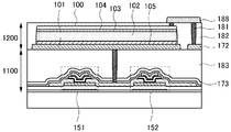
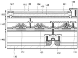
본 실시형태에서는 본 발명의 일 형태에 따른 광전 변환 소자(100)에 대하여 도면을 참조하여 설명한다.In the present embodiment, a
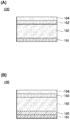
도 1의 (A)는 본 발명의 일 형태에 따른 광전 변환 소자(100)의 단면 구조를 모식적으로 나타낸 도면이다. 광전 변환 소자(100)는 제 1 전극(101), 제 1 전극(101) 위의 광전 변환층(102), 광전 변환층(102) 위의 정공 주입 저지층(103), 정공 주입 저지층(103) 위의 제 2 전극(104)을 가진다.1 (A) is a diagram schematically showing a cross-sectional structure of a
광전 변환 소자(100)는 기판 위에 형성되어도 좋고, 기판에 형성된 구동용 트랜지스터 위 또는 기판 위에 형성된 구동용 트랜지스터 위에 형성되어도 좋다.The
도 1의 (B)는 본 발명의 다른 일 형태에 따른 광전 변환 소자(100)의 단면 구조를 모식적으로 나타낸 도면이다. 광전 변환 소자(100)는 제 1 전극(101), 제 1 전극(101) 위의 전자 주입 저지층(105), 전자 주입 저지층(105) 위의 광전 변환층(102), 광전 변환층(102) 위의 정공 주입 저지층(103), 정공 주입 저지층(103) 위의 제 2 전극(104)을 가진다.1 (B) is a diagram schematically showing a cross-sectional structure of a
<제 1 전극(101)>≪
제 1 전극(101)은 예를 들어, 음극성 전극으로서 사용되는 전극이다. 제 1 전극(101)에는 예를 들어, 금, 질화 타이타늄, 몰리브데넘, 텅스텐 등을 사용할 수 있다. 또한, 예를 들어 알루미늄, 타이타늄, 또는 알루미늄을 타이타늄으로 끼운 적층을 사용할 수 있다. 제 1 전극(101)은 스퍼터링법이나 플라스마 CVD법으로 형성할 수 있다.The
또한, 도 1의 (A)에 도시된 제 1 전극(101)은, 광전 변환층(102)의 피복성 불량 등에 기인하는 제 2 전극(104)과의 단락을 방지하기 위하여, 평탄성이 높은 것이 바람직하다.The
평탄성이 높은 도전막으로서는 예를 들어, 실리콘이 1wt%~20wt% 첨가된 산화 인듐 주석막 등을 들 수 있다. 실리콘이 첨가된 산화 인듐 주석막의 평탄성이 높은 것은, 원자간력 현미경을 사용한 측정에 의하여 확인되었다. 350℃로 1시간 동안 가열 처리한 산화 인듐 주석막과, 동일한 처리를 행한 실리콘이 10wt% 첨가된 산화 인듐 주석막 각각의 2μm×2μm의 영역을 원자간력 현미경으로 측정한 결과, 전자(前者)의 최대 고저차(P-V)가 23.3nm인 한편, 후자는 7.9nm였다.As the conductive film having high flatness, for example, an indium tin oxide film in which 1 wt% to 20 wt% of silicon is added can be given. The high flatness of the silicon-doped indium tin oxide film was confirmed by measurement using an atomic force microscope. The area of 2 μm × 2 μm of each of the indium tin oxide film heat-treated at 350 ° C. for 1 hour and the indium tin oxide film doped with silicon at 10 wt% by the same treatment was measured by an atomic force microscope, (PV) of 23.3 nm, while the latter was 7.9 nm.
산화 인듐 주석막은 성막 시에 비정질이더라도 비교적 낮은 온도에서 결정화가 일어나기 때문에, 결정립 성장으로 인한 표면의 거칠어짐이 나타나기 쉽다. 한편, 실리콘이 첨가된 산화 인듐 주석막은 400℃를 넘는 가열 처리를 행하여도 X선 회절 분석에서 피크의 출현이 확인되지 않는다. 즉, 실리콘이 첨가된 산화 인듐 주석막은 비교적 높은 온도로 가열 처리를 행하여도 비정질 상태를 유지한다. 따라서, 실리콘이 첨가된 산화 인듐 주석막은 표면의 거칠어짐이 나타나기 어렵다.Since the indium tin oxide film undergoes crystallization at a relatively low temperature even if it is amorphous at the time of film formation, the surface is likely to be roughened due to grain growth. On the other hand, in the indium tin oxide film to which silicon is added, the appearance of a peak is not confirmed by X-ray diffraction analysis even when the heat treatment is performed at a temperature exceeding 400 캜. That is, the indium tin oxide film to which silicon is added maintains an amorphous state even when heat treatment is performed at a relatively high temperature. Therefore, the surface roughness of the indium tin oxide film to which silicon is added is unlikely to appear.
<광전 변환층(102)>≪
다음에, 광전 변환층(102)에 대하여 설명한다. 광전 변환층(102)에는 셀레늄계 재료를 사용할 수 있다. 셀레늄계 재료를 사용한 광전 변환 소자(100)는 가시광에 대한 외부 양자 효율이 높은 특성을 가진다. 애벌란시 현상에 의하여 상기 광전 변환 소자를, 입사하는 광량에 대한 전자의 증폭이 큰 고감도 센서로 할 수 있다. 또한, 셀레늄계 재료는 광 흡수 계수가 높기 때문에 광전 변환층(102)을 얇게 하기 쉽다는 이점을 가진다.Next, the
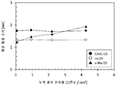
셀레늄계 재료에는 단결정 셀레늄과 비단결정 셀레늄이 있고, 비단결정 셀레늄에는 다결정 셀레늄, 미결정 셀레늄, 비정질 셀레늄(어모퍼스 셀레늄) 등이 있다. 광전 변환층(102)에는 이들 셀레늄을 사용할 수 있다. 또한, 결정 셀레늄과 비정질 셀레늄이 혼합된 셀레늄층을 형성하여 사용하여도 좋다. 결정 셀레늄층은 예를 들어, 비정질 셀레늄층을 성막한 후에 가열 처리를 행함으로써 얻을 수 있다. 또한, 광전 변환층(102)에 결정 셀레늄층을 사용하는 경우, 상기 층에 포함되는 셀레늄의 결정의 입경을 화소 피치보다 작게 함으로써 화소마다의 특성 편차를 저감할 수 있다. 또한, 결정 셀레늄층은 비정질 셀레늄층보다 가시광에 대한 분광 감도나 광 흡수 계수가 높은 특성을 가진다. 다만, 비정질 셀레늄층을 사용할 수도 있다.Selenium-based materials include monocrystalline selenium and non-crystalline selenium. Non-crystalline selenium includes polycrystalline selenium, microcrystalline selenium, and amorphous selenium (amos selenium). These selenium can be used for the
또한, 광전 변환층(102)은 구리, 인듐, 셀레늄의 화합물(CIS)을 포함하는 층이라도 좋다. 또는, 구리, 인듐, 갈륨, 셀레늄의 화합물(CIGS)을 포함하는 층이라도 좋다. CIS 및 CIGS를 사용하면 셀레늄 단체(單體)를 사용하는 경우와 마찬가지로, 애벌란시 현상을 이용할 수 있는 광전 변환 소자를 형성할 수 있다. CIS 및 CIGS는 p형 반도체이기 때문에, 접합을 형성하기 위하여 n형 반도체인 황화 카드뮴이나 황화 아연 등을 이와 접촉하도록 제공하여도 좋다. 애벌란시 현상을 발생시키기 위해서는, 광전 변환 소자에 비교적 높은 전압(예를 들어 10V 이상)을 인가하는 것이 바람직하다.The
<정공 주입 저지층(103)>≪ Hole
다음에, 본 발명의 일 형태에서의 정공 주입 저지층(103)에 대하여 설명한다. 정공 주입 저지층(103)은 제 2 전극(104)으로부터 광전 변환층(102)에 대한 정공의 주입을 억제하는 기능을 가지는 층이다.Next, the hole
종래에는, 상술한 셀레늄계 재료를 광전 변환층에 사용한 광전 변환 소자는 전계 인가 시에서의 암전류가 커서 시그널-노이즈(S/N)비가 낮다는 문제가 있었다. 여기서 암전류의 원인 중 하나로서, 전극으로부터 광전 변환층에 대한 전하의 주입을 억제하지 못했던 것을 들 수 있다. 그래서, 광전 변환층에 대한 전하의 주입을 억제하기 위하여, 산화 갈륨으로 구성되는 정공 주입 저지층을 광전 변환층과 전극 사이에 제공하는 구조가 제안되었다.Conventionally, the photoelectric conversion element using the above-described selenium-based material as the photoelectric conversion layer has a problem that the dark current at the time of applying an electric field is large and the signal-noise (S / N) ratio is low. One of the causes of the dark current is that the injection of the charge from the electrode into the photoelectric conversion layer can not be suppressed. Thus, a structure has been proposed in which a hole injection blocking layer composed of gallium oxide is provided between the photoelectric conversion layer and the electrode in order to suppress the injection of charges into the photoelectric conversion layer.
여기서 산화 갈륨층을 정공 주입 저지층으로서 충분히 기능시키기 위해서는, 정공 주입 저지층을 관통하는 터널 전류를 억제할 필요가 있고, 그것을 위해서는 이 층의 막 두께를 일정 이상으로 할 필요가 있다. 예를 들어, 5nm 이상 1μm 이하의 막 두께로 하는 것이 바람직하고, 10nm 이상 500nm 이하의 막 두께로 하는 것이 더 바람직하다.In order to sufficiently function the gallium oxide layer as the hole injection blocking layer in this case, it is necessary to suppress the tunnel current passing through the hole injection blocking layer. For this purpose, it is necessary to set the film thickness of this layer to a predetermined value or more. For example, the film thickness is preferably 5 nm or more and 1 μm or less, more preferably 10 nm or more and 500 nm or less.
그런데 산화 갈륨층을 형성하는 경우, 성막 장치 내부에서 산화 갈륨을 주성분으로 하는 파티클 형상의 이물이 적지 않게 발생된다.However, in the case of forming the gallium oxide layer, there is little foreign matter in the form of particles mainly composed of gallium oxide inside the film forming apparatus.
여기서 MOCVD(metal organic chemical vapor deposition)법으로 막 두께 5nm의 산화 갈륨을 형성하였을 때의 파티클 수의 계측 결과에 대하여 설명한다.Here, measurement results of the number of particles when gallium oxide with a thickness of 5 nm is formed by a metal organic chemical vapor deposition (MOCVD) method will be described.
우선, 계측의 개요를 설명한다. 먼저 5인치×5인치의 유리 기판을 준비하고, 유리 기판 검사 장치를 사용하여 기판 위의 파티클 수를 계측하였다. 다음에, 상기 기판을 MOCVD 장치로 반입하고 산화 갈륨층을 막 두께 5nm로 성막하고, 장치에서 유리 기판을 꺼내서 유리 기판 검사 장치를 사용하여 기판 위의 파티클 수를 다시 계측하였다. 그리고, 성막 전후에 있어서의 파티클의 증가 수를 구하였다.First, the outline of measurement will be described. First, a glass substrate of 5 inches by 5 inches was prepared, and the number of particles on the substrate was measured by using a glass substrate inspecting apparatus. Next, the substrate was loaded into an MOCVD apparatus, and a gallium oxide layer was formed to a film thickness of 5 nm. A glass substrate was taken out from the apparatus, and the number of particles on the substrate was measured again using a glass substrate inspection apparatus. Then, an increase in the number of particles before and after the film formation was determined.
계측의 조건에 대하여 자세히 설명한다. 유리 기판 검사 장치로서는 Hitachi High-Technologies Corporation 제조의 'GI4600'을 사용하여 유리 기판 위의 직경 1μm 이상의 파티클의 수를 계측하였다. MOCVD 장치로서는 WACOM R&D CORPORATION 제조의 'WMCHH-2127s'를 사용하였다. 성막의 원료 가스로서 TEG(triethylgallium)를 공급량 0.1ccm로, ECH(ethylcyclohexane)를 공급량 0.5ccm로, 산소를 공급량 2.0slm로 사용하고, 캐리어 가스로서 아르곤을 공급량 1.8slm로 사용하고, 퍼지 가스(purge gas)로서 질소를 공급량 0.38slm로 사용하였다. 성막 시의 기판 온도는 475℃로 하고, 장치 내의 압력은 1067Pa로 하여 성막하였다.The conditions of the measurement will be described in detail. As a glass substrate inspection apparatus, 'GI4600' manufactured by Hitachi High-Technologies Corporation was used to measure the number of particles having a diameter of 1 μm or more on a glass substrate. As the MOCVD apparatus, 'WMCHH-2127s' manufactured by WACOM R & D CORPORATION was used. TEG (triethylgallium) was supplied as a source gas for film formation at 0.1 ccm, ECH (ethylcyclohexane) was supplied at 0.5 ccm, oxygen was supplied at 2.0 slm, argon was used as a carrier gas at 1.8 slm, purge gas gas was used as the feed amount of 0.38 slm. The substrate temperature at the time of film formation was 475 캜, and the pressure in the apparatus was set at 1067 Pa.
성막은 3개의 유리 기판에 행하였고, 성막 전후에 있어서의 파티클의 증가 수는 각각 9개, 3개, 25개였다. 본 계측은 막 두께 5nm의 산화 갈륨층의 성막에 있어서 발생된 파티클 수의 계측이지만, 막 두께가 두꺼울수록 발생되는 파티클 수도 증가될 것으로 예상된다.The film formation was performed on three glass substrates, and the number of increase of particles before and after the film formation was 9, 3, and 25, respectively. This measurement is the measurement of the number of particles generated in the film formation of the gallium oxide layer with a film thickness of 5 nm, but it is expected that the larger the film thickness, the larger the number of particles generated.
상기 파티클은 광전 변환 소자에 들어가면 소자 내에서 이물로 작용하여, 일부의 화소가 정상적으로 기능하지 못하게 될 수 있다. 특히 8K 해상도 영상의 촬영에 사용되는 광전 변환 소자는 방대한 수의 화소로 구성되기 때문에, 하나의 화소가 매우 작게 제작된다. 예를 들어, 화소 하나의 크기를 3μm×3μm로 하였을 때, 성막 장치 내에서 발생된 크기 1μm의 파티클이 광전 변환 소자에 들어가는 것은 매우 큰 문제가 된다. 촬상 장치의 제조 수율에 직접 영향을 미친다.When the particles enter the photoelectric conversion element, they act as foreign matter in the element, and some pixels may not function normally. Especially, since the photoelectric conversion element used for photographing the 8K resolution image is composed of a large number of pixels, one pixel is made very small. For example, when one pixel has a size of 3
또한, 산화 갈륨층은 결정성이 낮은 것이 알려져 있다. 광전 변환 소자의 광전 변환층에 예를 들어, 결정 셀레늄계 재료를 사용하는 경우, 상기 광전 변환층과 접촉되는 정공 주입 저지층의 결정성이 낮으면, 양층의 계면에서 밀착성이 낮게 되어, 계면의 손상이나 박리가 생길 경우가 있다. 부분적으로 상기 층들 사이에서의 전하의 이동에 지장을 줄 수도 있다. 특히, 8K 해상도 영상의 촬영에 사용되는 광전 변환 소자에서는 하나의 화소가 매우 작게 제작되기 때문에, 상기 문제가 현저해진다. 화소 하나가 차지하는 영역에 있어서, 상기 광전 변환층과 정공 주입 저지층과의 밀착성이 낮은 1μm×1μm의 면적의 영역이 생겼을 때, 예를 들어 화소 하나의 크기가 3μm×3μm인 경우는, 화소의 크기가 그보다 큰 경우에 비하여 상기 문제의 영향이 현저해진다.It is also known that the gallium oxide layer has a low crystallinity. When a crystalline selenium-based material is used for the photoelectric conversion layer of the photoelectric conversion element, for example, when the crystallinity of the hole injection blocking layer in contact with the photoelectric conversion layer is low, the adhesion at the interface between the two layers becomes low, Damage or peeling may occur. It may interfere partially with the movement of charges between the layers. Particularly, in the photoelectric conversion element used for photographing the 8K-resolution image, since one pixel is made very small, the above problem becomes conspicuous. When a region having an area of 1
또한, 성막 후의 가열 처리에 의하여 산화 갈륨층의 결정성을 향상시킬 수도 있다. 또한, MOCVD로 산화 갈륨을 성막하는 경우, 성막 온도가 낮으면 탄소나 수소가 막 내에 많이 들어가기 때문에, 성막 온도를 높게 할 필요가 있다. 어쨌든 고품질의 산화 갈륨층을 형성하고자 하는 경우, 고온으로 가열 처리를 행할 필요가 있다. 하지만, 산화 갈륨층의 피형성층이 되는 광전 변환층에 셀레늄계 재료를 사용하는 경우에는, 셀레늄의 융점이 낮은(221℃) 것으로 인하여 승화가 일어나기 쉽기 때문에, 광전 변환층에 고온으로 가열 처리를 행하면 손상이 생겨 문제가 될 수 있다.Further, the crystallinity of the gallium oxide layer can be improved by a heat treatment after film formation. Further, when gallium oxide is formed by MOCVD, when the film forming temperature is low, carbon and hydrogen are contained in a large amount in the film, and therefore it is necessary to raise the film forming temperature. In any case, when a high-quality gallium oxide layer is to be formed, it is necessary to perform the heat treatment at a high temperature. However, when a selenium-based material is used for the photoelectric conversion layer serving as the layer to be formed of the gallium oxide layer, since the selenium has a low melting point (221 캜), sublimation tends to occur. Damage can occur and cause problems.
그러므로, 본 발명의 일 형태에서는 정공 주입 저지층(103)에, 성막 중에서의 파티클 발생량이 산화 갈륨보다 적은 재료를 사용한다. 또한, 정공 주입 저지층(103)에는 산화 갈륨의 결정성보다 광전 변환층(102)의 결정성에 더 가까운 결정성을 가지는 재료를 사용한다. 또한, 정공 주입 저지층(103)에는 광전 변환층(102)에 큰 손상을 주지 않고 고품질의 막을 형성할 수 있는 재료를 사용한다.Therefore, in one embodiment of the present invention, a material in which the amount of particles generated in the film formation is smaller than that of gallium oxide is used for the hole
특히, 본 발명의 일 형태에서는 정공 주입 저지층(103)에 산화물 재료를 사용한다. 정공 주입 저지층(103)에 사용하는 산화물 재료로서는 산화 인듐, 산화 주석, 산화 아연, In-Zn 산화물, Sn-Zn 산화물, Al-Zn 산화물, Zn-Mg 산화물, Sn-Mg 산화물, In-Mg 산화물, In-Ga 산화물, In-Ga-Zn 산화물, In-Al-Zn 산화물, In-Sn-Zn 산화물, Sn-Ga-Zn 산화물, Al-Ga-Zn 산화물, Sn-Al-Zn 산화물, In-Hf-Zn 산화물, In-La-Zn 산화물, In-Ce-Zn 산화물, In-Pr-Zn 산화물, In-Nd-Zn 산화물, In-Sm-Zn 산화물, In-Eu-Zn 산화물, In-Gd-Zn 산화물, In-Tb-Zn 산화물, In-Dy-Zn 산화물, In-Ho-Zn 산화물, In-Er-Zn 산화물, In-Tm-Zn 산화물, In-Yb-Zn 산화물, In-Lu-Zn 산화물, In-Sn-Ga-Zn 산화물, In-Hf-Ga-Zn 산화물, In-Al-Ga-Zn 산화물, In-Sn-Al-Zn 산화물, In-Sn-Hf-Zn 산화물, In-Hf-Al-Zn 산화물을 들 수 있다.Particularly, in one embodiment of the present invention, an oxide material is used for the hole
또한 여기서, 예를 들어 In-Ga-Zn 산화물이란, In, Ga, Zn을 주성분으로서 가지는 산화물을 의미한다. 또한, In, Ga, Zn 이외의 금속 원소가 들어 있어도 좋다. 또한, 본 명세서에서 In-Ga-Zn 산화물로 구성된 막을 IGZO막이라고도 부른다.Here, for example, the In-Ga-Zn oxide means an oxide having In, Ga, and Zn as main components. In addition, metal elements other than In, Ga, and Zn may be contained. In this specification, a film composed of an In-Ga-Zn oxide is also referred to as an IGZO film.
정공 주입 저지층(103)에 사용하는 산화물로서는 In-Ga-Zn 산화물이 특히 유용하다. In-Ga-Zn 산화물은 CAAC(c-axis aligned crystalline) 구조를 가지는 막, 또는 미결정 산화물막이 될 경향이 있으므로, 정공 주입 저지층(103)에 In-Ga-Zn 산화물을 사용하면 결정을 가지는 막이 되어 결정을 가지는 광전 변환층(102)과의 상성(相性)이 좋아지므로 바람직하다. 또한, In-Ga-Zn 산화물은 In, Ga, Zn, 및 O를 적어도 가진다.As the oxide used for the hole
특히 CAAC 구조를 가지는 막은 후술하는 바와 같이 결정성이 높고, 예를 들어 광전 변환층(102)이 결정 셀레늄층인 경우에는, 양자의 결정성이 공통됨으로써 정공 주입 저지층(103)이 되는 CAAC 구조를 가지는 막이 형성되기 쉽고 계면의 밀착성이 높아지므로 바람직하다.In particular, when the
또한, 정공 주입 저지층(103)에 사용할 수 있는 In-Ga-Zn 산화물은 다양한 조성으로 할 수 있다. 예를 들어, In:Ga:Zn=1:3:2, 1:3:3, 1:3:4, 1:3:6, 1:4:5, 1:6:4, 또는 1:9:6(원자수비) 등의 In-Ga-Zn 산화물 등을 사용할 수 있다. 또한, 정공 주입 저지층(103)에는 In:Ga:Zn=1:1:1, 2:1:3, 5:5:6, 또는 3:1:2(원자수비) 등의 In-Ga-Zn 산화물 등을 사용할 수 있다.In addition, the In-Ga-Zn oxide that can be used for the hole
또한, 정공 주입 저지층(103)에 사용하는 산화물의 막은 대표적으로는 스퍼터링법이나 플라스마 CVD법으로 형성할 수 있지만, 다른 방법, 예를 들어 열 CVD법으로 형성하여도 좋다. 열 CVD법의 예로서는 MOCVD법이나 ALD(atomic layer deposition)법 등이 있다.The oxide film used for the hole
열 CVD법은, 플라스마를 사용하지 않는 성막 방법이기 때문에, 플라스마 대미지에 기인한 결함이 생성되지 않는다는 이점이 있다. 또한 열 CVD법의 경우, 원료 가스와 산화제를 체임버 내로 동시에 공급하고, 체임버 내를 대기압 또는 감압하로 하고, 기판 부근 또는 기판 위에서 반응을 일으켜 기판 위에 퇴적시킴으로써 성막하여도 좋다.Since the thermal CVD method is a film formation method that does not use plasma, there is an advantage that defects due to plasma damage are not generated. Further, in the case of the thermal CVD method, the film may be formed by simultaneously supplying the source gas and the oxidizing agent into the chamber, and causing the reaction in the vicinity of the substrate or on the substrate to be deposited on the substrate under the atmospheric pressure or reduced pressure.
또한, 산화물의 성막에는 대향 타깃식 스퍼터링 장치를 사용할 수도 있다. 대향 타깃식 스퍼터링 장치를 사용한 성막법을 VDSP(vapor deposition SP)라고 부를 수도 있다.An opposite target sputtering apparatus may also be used for forming the oxide. The deposition method using the opposite target sputtering apparatus may be referred to as VDSP (vapor deposition SP).
또한, 산화물의 성막 방법이나 물성에 대해서는 후술하는 실시형태에서 자세히 설명한다.The method of forming the oxide and the physical properties thereof will be described in detail in the following embodiments.
<제 2 전극(104)>≪
다음에, 제 2 전극(104)에 대하여 설명한다. 제 2 전극(104)은 예를 들어 정극성 전극으로서 사용되는 전극이다. 예를 들어 인듐 주석 산화물, 실리콘을 포함하는 인듐 주석 산화물, 아연을 포함하는 산화 인듐, 산화 아연, 갈륨을 포함하는 산화 아연, 알루미늄을 포함하는 산화 아연, 산화 주석, 플루오린을 포함하는 산화 주석, 안티모니를 포함하는 산화 주석, 또는 그래핀 등을 사용할 수 있지만, 인듐 주석 산화물, 실리콘을 포함하는 인듐 주석 산화물이 특히 바람직하다. 제 2 전극(104)은 단층에 한정되지 않고 다른 막들의 적층이라도 좋다. 또한, 인듐 주석 산화물은 In, Sn, O를 가진다.Next, the
광을 광전 변환층(102)에 도달하게 하기 위하여, 제 2 전극(104)은 광의 투과성이 높은 것이 바람직하다. 특히, 8K 촬상 장치에서는 화소 하나가 차지하는 면적이 매우 작고, 수광에 사용할 수 있는 영역이 매우 작기 때문에, 광의 투과성이 더 중요하다. 제 2 전극(104)은 스퍼터링법이나 플라스마 CVD법으로 형성할 수 있다.In order to allow light to reach the
<전자 주입 저지층(105)>≪ Electron
전자 주입 저지층(105)에 대하여 설명한다. 전자 주입 저지층(105)은 제 1 전극(101)으로부터 광전 변환층(102)에 대한 전자의 주입을 억제하는 기능을 가지는 층이다. 전자 주입 저지층(105)에는 산화 니켈 또는 황화 안티모니 등을 사용하는 구성으로 할 수도 있다.The electron
<광전 변환 소자의 밴드 구조>≪ Band Structure of Photoelectric Conversion Element &
다음에, 도 1의 (A)에 도시된 광전 변환 소자(100)의 밴드 구조에 대한 개념도를 도 2에 나타내었다. 도 2의 개념도는, 광전 변환층(102)에 결정성의 Se를, 정공 주입 저지층(103)에 산화물인 IGZO막(예를 들어 In:Ga:Zn=1:3:6(원자수비))을, 제 2 전극(104)에 인듐 주석 산화물을 사용하였을 때의 밴드 구조를 늘어놓은 도면이다. 또한, IGZO막은 조성이나 결정 구조 등에 따라 페르미 준위가 어느 정도 변화된다. 따라서, 목적의 정공 주입 저지층(103)이 필요로 하는 물성을 가지게 되도록, IGZO막의 조성이나 결정 구조 등을 적절히 선택하여 형성할 수도 있다.Next, a conceptual diagram of the band structure of the
여기서, 셀레늄의 전자 친화력(진공 준위에서 전도대 하단까지의 에너지 차)은 약 3.5eV, 에너지 갭이 1.8eV~2.0eV 사이에 있는 것이 알려져 있다. 또한, IGZO막(In:Ga:Zn=1:3:6(원자수비))의 전자 친화력은 약 4.5eV, 에너지 갭은 3.3eV이다. 또한, 인듐 주석 산화물의 일 함수는 4.7eV인 것이 알려져 있다. 그러므로, 각 밴드 구조의 관계는 도 2에 나타낸 구조가 된다.Here, it is known that the electron affinity of selenium (energy difference from the vacuum level to the lower end of the conduction band) is about 3.5 eV and the energy gap is between 1.8 eV and 2.0 eV. The electron affinity of the IGZO film (In: Ga: Zn = 1: 3: 6 (atomic ratio)) is about 4.5 eV and the energy gap is 3.3 eV. It is also known that the work function of the indium tin oxide is 4.7 eV. Therefore, the relationship of each band structure becomes the structure shown in Fig.
정공 주입 저지층(103)에 착안한다. 도 2를 보면 알 수 있듯이, 제 2 전극(104)으로부터의 정공의 주입은 IGZO막의 큰 장벽에 의하여 억제된다. 그러므로, 광전 변환 소자(100)의 암전류가 저감되어 S/N비가 개선되는 것을 이해할 수 있다. 따라서, 광전 변환 소자(100)를 탑재한 본 발명의 일 형태에 따른 촬상 소자는 촬상 성능이 향상되고, 저조도 하에서의 촬상이 용이해진다.Attention is focused on the hole
또한, 도 21의 (A) 및 (B)에 각종 IGZO막의 전자 친화력과 에너지 갭을 나타내었다. 도면에 나타낸 바와 같이, In:Ga:Zn=1:3:6(원자수비) 이외의 조성을 가지는 IGZO막도 정공 주입 저지층으로서 기능할 수 있는 것을 이해할 수 있다.21 (A) and (B) show the electron affinity and energy gap of various IGZO films. As shown in the figure, it can be understood that an IGZO film having a composition other than In: Ga: Zn = 1: 3: 6 (atomic ratio) can also function as a hole injection blocking layer.
본 실시형태에 기재된 구성은 다른 실시형태에 기재된 구성과 적절히 조합하여 사용할 수 있다.The configuration described in this embodiment mode can be used in appropriate combination with the configuration described in the other embodiments.
(실시형태 2)(Embodiment 2)
다음에, 본 발명의 일 형태에 따른 촬상 장치의 구체적인 구성예에 대하여 도면을 참조하여 설명한다. 도 3의 (A)는 본 발명의 일 형태에 따른 촬상 장치의 단면도의 일례이며, 도 1에 도시된 광전 변환 소자(100)와 구동용으로 사용되는 트랜지스터의 구체적인 접속 형태의 일례를 도시한 것이다. 상기 촬상 장치는 트랜지스터(151) 및 트랜지스터(152)가 제공되는 층(1100)과, 광전 변환 소자(100)가 제공되는 층(1200)을 가진다.Next, a specific configuration example of an image pickup apparatus according to an embodiment of the present invention will be described with reference to the drawings. 3 (A) is an example of a cross-sectional view of an image pickup apparatus according to an embodiment of the present invention, and shows an example of a specific connection form of the
또한, 본 실시형태에서 참조하는 단면도에서는 각 배선, 각 전극, 및 각 도전체를 개별의 요소로 도시하였지만, 이들이 전기적으로 접속되는 경우에는 동일한 요소로서 제공되는 경우도 있다. 또한, 트랜지스터의 게이트 전극, 소스 전극, 또는 드레인 전극이 도전체를 통하여 각 배선과 접속되는 형태는 일례에 불과하고, 트랜지스터의 게이트 전극, 소스 전극, 또는 드레인 전극 각각이 배선으로서의 기능을 가지는 경우도 있다.In the cross-sectional view referred to in the present embodiment, each wire, each electrode, and each conductor are shown as individual elements, but they may be provided as the same element when they are electrically connected. Further, a mode in which the gate electrode, the source electrode, or the drain electrode of the transistor is connected to each wiring through a conductor is merely an example, and even when each of the gate electrode, the source electrode, or the drain electrode of the transistor has a function as a wiring have.
또한, 각 요소 위에는 보호막, 층간 절연막, 또는 평탄화막으로서의 기능을 가지는 절연층(182) 및 절연층(183) 등이 제공된다. 예를 들어, 절연층(182) 및 절연층(183) 등에는 산화 실리콘막, 산화 질화 실리콘막 등의 무기 절연막을 사용할 수 있다. 또는, 아크릴 수지, 폴리이미드 수지 등의 유기 절연막 등을 사용하여도 좋다. 절연층(182) 및 절연층(183) 등의 상면에는 필요에 따라 CMP(chemical mechanical polishing)법 등에 의하여 평탄화 처리를 행하는 것이 바람직하다.An insulating
또한, 도면에 도시된 배선 등의 일부가 제공되지 않는 경우나, 도면에 도시되지 않은 배선 등이나 트랜지스터 등이 각 층에 포함되는 경우도 있다. 또한, 도면에 도시되지 않은 층이 이 적층 구조에 포함되는 경우도 있다. 또한, 도면에 도시된 층의 일부가 포함되지 않는 경우도 있다.In addition, there may be cases where a part of the wiring or the like shown in the drawing is not provided, or a wiring or the like not shown in the drawing is included in each layer. In addition, a layer not shown in the drawing may be included in this laminated structure. Also, some of the layers shown in the drawings may not be included.
트랜지스터(151) 및 트랜지스터(152)에는 산화물을 반도체로서 사용한 트랜지스터(OS 트랜지스터)를 사용하는 것이 특히 바람직하다.It is particularly preferable to use a transistor (OS transistor) using an oxide as a semiconductor for the
OS 트랜지스터는 매우 낮은 오프 전류 특성을 가지기 때문에, 촬상의 다이내믹 레인지를 확대할 수 있다. 산화물 반도체를 사용한 트랜지스터는 오프 전류가 매우 낮기 때문에, 게이트 전위가 매우 작은 경우에도 상기 게이트 전위에 따른 전류를 정확하게 출력할 수 있다. 따라서, 검출할 수 있는 조도의 레인지, 즉 다이내믹 레인지를 넓힐 수 있다.Since the OS transistor has a very low off current characteristic, the dynamic range of image pickup can be increased. Since the transistor using the oxide semiconductor has a very low off current, the current corresponding to the gate potential can be accurately outputted even when the gate potential is very small. Therefore, the range of illuminance that can be detected, that is, the dynamic range can be widened.
또한, 트랜지스터(151) 및 트랜지스터(152)가 가지는 낮은 오프 전류 특성에 의하여, 전하 축적부에서 전하가 유지될 수 있는 기간을 매우 길게 할 수 있다. 그러므로, 회로 구성이나 동작 방법을 복잡하게 하지 않고, 전하의 축적 동작을 모든 화소에서 동시에 행하는 글로벌 셔터 방식을 적용할 수 있다.Further, due to the low off current characteristics of the
일반적으로 화소가 매트릭스 형태로 배치된 촬상 장치의 경우, 도 22의 (A)에 도시된 촬상 동작(111), 데이터 유지 동작(112), 판독 동작(113)을 행마다 행하는 구동 방법인 롤링 셔터 방식이 사용된다. 롤링 셔터 방식을 사용하는 경우에는 촬상의 동시성이 소실되기 때문에, 피사체가 움직이는 경우에는 화상에 왜곡이 생긴다.Generally, in the case of an image pickup apparatus in which pixels are arranged in a matrix form, the
따라서, 본 발명의 일 형태에서는 도 22의 (B)에 도시된 촬상 동작(111)을 모든 행에서 동시에 행하고 판독 동작(113)을 행마다 순차적으로 행할 수 있는 글로벌 셔터 방식을 사용하는 것이 바람직하다. 글로벌 셔터 방식을 사용함으로써, 촬상 장치의 각 화소에서의 촬상의 동시성을 확보할 수 있으므로, 피사체가 움직이는 경우에도 왜곡이 작은 화상을 용이하게 얻을 수 있다. 또한, 글로벌 셔터 방식에서는 노광 시간(전하의 축적 동작을 하는 기간)을 길게 할 수도 있기 때문에 저조도 환경에서의 촬상에도 적합하다.Therefore, in one form of the present invention, it is preferable to use the global shutter method in which the
또한, OS 트랜지스터는 활성 영역 또는 활성층에 실리콘을 사용한 트랜지스터(이하, Si 트랜지스터)보다 전기 특성 변동의 온도 의존성이 작기 때문에, 매우 넓은 온도 범위에서 사용할 수 있다. 따라서, OS 트랜지스터를 가지는 촬상 장치 및 반도체 장치는 자동차, 항공기, 우주기 등에 탑재하기에도 적합하다.Further, the OS transistor can be used in a very wide temperature range because the temperature dependency of the electric characteristic fluctuation is smaller than that of a transistor (hereinafter, Si transistor) using silicon in the active region or the active layer. Therefore, the imaging device and the semiconductor device having the OS transistor are also suitable for mounting on an automobile, an aircraft, a spacecraft, and the like.
또한, OS 트랜지스터는 Si 트랜지스터보다 드레인 내압이 높은 특성을 가진다. 셀레늄계 재료를 광전 변환층에 사용한 광전 변환 소자의 경우, 애벌란시 현상이 쉽게 일어나도록 비교적 높은 전압(예를 들어 10V 이상)을 인가하는 것이 바람직하다. 따라서 OS 트랜지스터와, 셀레늄계 재료를 광전 변환층에 사용한 광전 변환 소자를 조합함으로써 신뢰성이 높은 촬상 장치로 할 수 있다.The OS transistor has a higher drain breakdown voltage than the Si transistor. In the case of a photoelectric conversion device using a selenium-based material in the photoelectric conversion layer, it is preferable to apply a relatively high voltage (for example, 10 V or more) so that aeration can be easily caused. Therefore, by combining the OS transistor and the photoelectric conversion element using the selenium-based material as the photoelectric conversion layer, a highly reliable imaging device can be obtained.
또한, 도 3의 (A)에는 각 트랜지스터가 백 게이트를 가지는 형태를 예시하였지만, 도 3의 (B)에 도시된 바와 같이 백 게이트를 가지지 않는 형태로 하여도 좋다. 또한, 도 3의 (C)에 도시된 바와 같이 일부의 트랜지스터, 예를 들어 트랜지스터(151)만이 백 게이트를 가지는 형태라도 좋다. 이 백 게이트는 대향하여 제공되는 트랜지스터의 프런트 게이트와 전기적으로 접속되는 경우가 있다. 또는 이 백 게이트에 프런트 게이트와는 다른 고정 전위가 공급되는 경우가 있다. 또한, 이 백 게이트의 유무에 관한 형태는, 본 실시형태에서 설명하는 다른 촬상 장치의 형태에도 적용될 수 있다.3 (A), each transistor has a back gate. However, as shown in FIG. 3 (B), the transistor may have no back gate. Further, as shown in FIG. 3C, only some of the transistors, for example, the
층(1200)에 제공되는 광전 변환 소자(100)로서는, 다양한 형태의 소자를 사용할 수 있다. 도 3의 (A)에는 셀레늄계 재료를 광전 변환층(102)에 사용한 형태를 도시하였다. 셀레늄계 재료를 사용한 광전 변환 소자(100)는 가시광에 대한 외부 양자 효율이 높은 특성을 가진다. 애벌란시 현상에 의하여 상기 광전 변환 소자를, 입사하는 광량에 대한 전자의 증폭이 큰 고감도 센서로 할 수 있다. 또한, 셀레늄계 재료는 광 흡수 계수가 높기 때문에 광전 변환층(102)을 얇게 하기 쉽다는 이점을 가진다.As the
광전 변환 소자(100)의 각 층에는 실시형태 1에 기재된 재료를 사용할 수 있다.The material described in
또한, 도 3의 (A)에서는 광전 변환층(102) 및 투광성을 가지는 제 2 전극(104)을 광전 변환 소자 사이에서 분리하지 않는 구성으로 하였지만, 도 4의 (A)에 도시된 바와 같이 광전 변환 소자 사이에서 분리하는 구성으로 하여도 좋다. 또한, 화소 사이에서 제 1 전극(101)을 가지지 않는 영역에는 절연체를 사용하여 격벽(167)을 제공함으로써 광전 변환층(102) 및 투광성을 가지는 제 2 전극(104)에 균열이 생기지 않도록 하는 것이 바람직하지만, 도 4의 (B)에 도시된 바와 같이 격벽(167)을 제공하지 않는 구성으로 하여도 좋다. 또한, 도 3의 (A)에는 투광성을 가지는 제 2 전극(104)과 배선(172) 사이에 배선(188) 및 도전체(181)가 개재(介在)되는 구성을 도시하였지만, 도 4의 (C) 및 (D)에 도시된 바와 같이 투광성을 가지는 제 2 전극(104)과 배선(172)이 직접 접촉되는 형태로 하여도 좋다.3 (A), the
또한, 도 3의 (A), 도 4의 (A)~(D)에 도시된 제 1 전극(101)은, 광전 변환층(102)의 피복성 불량 등에 기인하는, 투광성을 가지는 제 2 전극(104)과의 단락을 방지하기 위하여, 평탄성이 높은 것이 바람직하다.The
또한, 격벽(167)은 무기 절연체나 절연 유기 수지 등을 사용하여 형성할 수 있다. 또한, 격벽(167)은 트랜지스터 등에 대한 차광을 위하여, 및/또는 화소 하나당 수광부의 면적을 확정하기 위하여, 흑색 등으로 착색되어도 좋다.Further, the
또한, 광전 변환 소자(100)에 정공 주입 저지층(103)에 더하여 전자 주입 저지층을 사용하여도 좋다.The electron injection blocking layer may be used for the
예를 들어, 도 5는 광전 변환 소자(100)에 정공 주입 저지층(103) 및 전자 주입 저지층(105)을 사용한 예이다. 상기 광전 변환 소자는 전자 주입 저지층(105), 광전 변환층(102), 및 정공 주입 저지층(103)이 순차적으로 적층된 구성을 가진다. 광전 변환층(102)은 결정 셀레늄층으로 하는 것이 바람직하다. 또한, 정공 주입 저지층(103)에는 실시형태 1에 기재된 재료를 사용할 수 있다. 또한, 전자 주입 저지층(105)에는 산화 니켈 또는 황화 안티모니 등을 사용하는 구성으로 할 수도 있다.For example, FIG. 5 shows an example in which the hole
도 5에 도시된 광전 변환 소자(100)에서는 전자 주입 저지층(105)이, 트랜지스터(151) 및 트랜지스터(152)와의 전기적인 접속을 가지는 제 1 전극(101)과 전기적인 접속을 가진다. 또한 투광성을 가지는 제 2 전극(104)이, 배선(188) 및 도전체(181)를 통하여 배선(172)과 전기적인 접속을 가진다.In the
또한, 정공 주입 저지층(103) 및 전자 주입 저지층(105)을 가지는 광전 변환 소자(100)의 구성, 그리고 광전 변환 소자(100)와 배선의 접속 형태는 도 6의 (A)~(F)에 예시된 것이라도 좋다. 또한, 광전 변환 소자(100)의 구성, 및 광전 변환 소자(100)와 배선의 접속 형태는 이들에 한정되지 않고, 다른 형태라도 좋다.The configuration of the
도 6의 (A)는 광전 변환 소자(100)에 정공 주입 저지층(103)과 접촉되는 투광성을 가지는 제 2 전극(104)이 제공되는 구성이다. 투광성을 가지는 제 2 전극(104)은 전극으로서 작용하며, 광전 변환 소자(100)의 출력 전류를 높일 수 있다.6A shows a structure in which a
투광성을 가지는 제 2 전극(104)에는 예를 들어, 인듐 주석 산화물, 실리콘을 포함하는 인듐 주석 산화물, 아연을 포함하는 산화 인듐, 산화 아연, 갈륨을 포함하는 산화 아연, 알루미늄을 포함하는 산화 아연, 산화 주석, 플루오린을 포함하는 산화 주석, 안티모니를 포함하는 산화 주석, 또는 그래핀 등을 사용할 수 있다. 또한, 투광성을 가지는 제 2 전극(104)은 단층에 한정되지 않고 다른 막들의 적층이라도 좋다.For example, indium tin oxide, indium tin oxide containing silicon, indium oxide containing zinc, zinc oxide, zinc oxide containing gallium, zinc oxide containing aluminum, Tin oxide, tin oxide containing fluorine, tin oxide containing antimony, or graphene can be used. The
도 6의 (B)는 투광성을 가지는 제 2 전극(104)과 배선(188)이 전기적인 접속을 가지는 구성이다.6 (B) shows a structure in which the
도 6의 (C)는 광전 변환 소자(100)에 정공 주입 저지층(103)과 접촉되는 투광성을 가지는 제 2 전극(104)이 제공되고, 또한 투광성을 가지는 제 2 전극(104)과 배선(188)이 전기적인 접속을 가지는 구성이다.6C shows a structure in which a
도 6의 (D)는 광전 변환 소자(100)를 덮는 절연층에, 정공 주입 저지층(103)이 노출되는 개구부가 제공되고, 상기 개구부를 덮는 투광성을 가지는 제 2 전극(104)과 배선(188)이 전기적인 접속을 가지는 구성이다.6D shows an example in which the insulating layer covering the
도 6의 (E)는 도 6의 (A)에 도시된 광전 변환 소자(100)의 적층 구조를 상하 반대로 한 구성이다. 투광성을 가지는 제 2 전극(104)을 통하여 외광을 수광하여도 좋고, 이 경우에는 도 6의 (E)의 광전 변환 소자(100)가 기판 측으로부터의 광을 수광하는 소자가 되기 때문에, 기판도 투광성을 가지는 구성으로 한다.FIG. 6E shows a structure in which the stacked structure of the
도 6의 (F)는, 도 6의 (E)의 광전 변환 소자(100)에서 전자 주입 저지층을 없앤 구성이다.FIG. 6F shows a structure in which the electron injection blocking layer is removed from the
또한, 도 6의 (E) 및 (F)에 도시된 광전 변환 소자(100)는, 정공 주입 저지층(103)이 투광성을 가지는 제 2 전극(104) 위에 형성되는 구성이다. 예를 들어, 투광성을 가지는 제 2 전극으로서 산화 인듐 주석막 또는 실리콘이 첨가된 산화 인듐 주석막을 사용하고, 정공 주입 저지층에 In-Ga-Zn 산화물 등을 사용하는 경우, 정공 주입 저지층(103) 및 제 2 전극(104)이 모두 인듐을 사용한 산화물이고 조성이 가깝기 때문에, 양자의 상성이 좋다. 즉, 정공 주입 저지층(103)과 제 2 전극(104)의 밀착성이 향상되어, 양자의 계면이 양호한 성질을 가지게 된다.The
또한, 제 2 전극(104)이 결정을 가지는 구조인 경우, 정공 주입 저지층(103)의 결정성을 용이하게 높일 수 있다. 또한, 정공 주입 저지층(103)이 결정을 가지는 구조이면 광전 변환층(102)의 결정성을 용이하게 높일 수 있다. 따라서, 광전 변환층(102)과 정공 주입 저지층(103)의 밀착성이 향상되어, 양자의 계면이 양호한 성질을 가지게 된다.When the
따라서, 예를 들어 투광성을 가지는 제 2 전극으로서 산화 인듐 주석막 또는 실리콘이 첨가된 산화 인듐 주석막을 사용하고, 정공 주입 저지층에 In-Ga-Zn 산화물 등을 사용하고, 광전 변환층(102)을 결정 셀레늄층으로 하면, 광전 변환 소자(100)를 구성하는 각 층들의 계면이 양호한 성질을 가지게 되어 내구성이 향상된다.Thus, for example, an indium tin oxide film or an indium tin oxide film doped with silicon is used as the second electrode having a light-transmitting property, an In-Ga-Zn oxide or the like is used as the hole injection blocking layer, Is a crystalline selenium layer, the interface between the layers constituting the
상술한 셀레늄계 재료나 비정질 실리콘 등을 사용하여 형성한 광전 변환 소자(100)는, 성막 공정, 리소그래피 공정, 에칭 공정 등 일반적인 반도체 제작 공정에 의하여 제작할 수 있다. 또한, 셀레늄계 재료는 저항이 높기 때문에, 도 3의 (A)에 도시된 바와 같이 광전 변환층(102)을 회로 사이에서 분리하지 않는 구성으로 할 수도 있다. 따라서, 본 발명의 일 형태에 따른 촬상 장치는 높은 수율, 저렴한 코스트로 제작할 수 있다. 한편, 실리콘 기판을 광전 변환층으로 한 포토다이오드를 형성하는 경우, 연마 공정이나 접합 공정 등 난도가 높은 공정이 필요하다.The
또한, 본 발명의 일 형태에 따른 촬상 장치는, 회로가 형성된 실리콘 기판(130)에 적층되는 구성으로 하여도 좋다. 예를 들어, 도 7의 (A)에 도시된 바와 같이 실리콘 기판(130)에 활성 영역을 가지는 트랜지스터(131) 및 트랜지스터(132)를 가지는 층(1400)이 화소 회로와 중첩되는 구성으로 할 수 있다. 또한, 도 7의 (B)는 트랜지스터의 채널 폭 방향의 단면도에 상당한다.The imaging device according to an embodiment of the present invention may be configured to be stacked on a
여기서 도 7의 (A) 및 (B)에는 Si 트랜지스터가 핀(fin)형인 구성을 예시하였지만 도 8의 (A)에 도시된 바와 같이 플레이너형이라도 좋다. 또는, 도 8의 (B)에 도시된 바와 같이 실리콘 박막의 활성층(135)을 가지는 트랜지스터라도 좋다. 또한, 활성층(135)은 다결정 실리콘이나 SOI(silicon on insulator)의 단결정 실리콘으로 할 수 있다.7A and 7B illustrate the structure in which the Si transistor is fin-shaped, but it may be a planer type as shown in FIG. 8A. Alternatively, a transistor having an
또한, 실리콘 기판(130)은 벌크 실리콘 기판에 한정되지 않고, 저마늄, 실리콘 저마늄, 탄소화 실리콘, 갈륨 비소, 알루미늄 갈륨 비소, 인화 인듐, 질화 갈륨, 유기 반도체를 재료로 한 기판을 사용할 수도 있다.The
여기서, 도 7의 (A)에 도시된 바와 같이, 산화물 반도체를 가지는 트랜지스터가 형성되는 영역과, Si 트랜지스터가 형성되는 영역 사이에는 절연층(180)이 제공된다.Here, as shown in Fig. 7A, an insulating
트랜지스터(131) 및 트랜지스터(132)의 활성 영역 부근에 제공되는 절연층 내의 수소는 실리콘의 댕글링 본드를 종단시킨다. 따라서 이 수소는 트랜지스터(131) 및 트랜지스터(132)의 신뢰성을 향상시키는 효과를 가진다. 한편, 트랜지스터(151) 등의 활성층인 산화물 반도체층 부근에 제공되는 절연층 내의 수소는, 산화물 반도체층 내에 캐리어를 생성하는 요인 중 하나가 된다. 그러므로 이 수소는 트랜지스터(151) 등의 신뢰성을 저하시키는 요인이 되는 경우가 있다. 따라서 실리콘계 반도체 재료를 사용한 트랜지스터를 가지는 한쪽 층과, 산화물 반도체를 사용한 트랜지스터를 가지는 다른 쪽 층을 적층하는 경우, 이들 사이에 수소의 확산을 방지하는 기능을 가지는 절연층(180)을 제공하는 것이 바람직하다. 절연층(180)에 의하여 한쪽 층에 수소를 가둠으로써 트랜지스터(131) 및 트랜지스터(132)의 신뢰성을 향상시킬 수 있다. 또한, 한쪽 층으로부터 다른 쪽 층으로 수소가 확산되는 것이 억제됨으로써 트랜지스터(151) 등의 신뢰성도 향상시킬 수 있다.The hydrogen in the insulating layer provided near the active region of
절연층(180)에는, 예를 들어 산화 알루미늄, 산화 질화 알루미늄, 산화 갈륨, 산화 질화 갈륨, 산화 이트륨, 산화 질화 이트륨, 산화 하프늄, 산화 질화 하프늄, 이트리아 안정화 지르코니아(YSZ) 등을 사용할 수 있다.As the insulating
또한, 도 7의 (A)에 도시된 구성에서는 실리콘 기판(130)에 형성되는 회로(예를 들어 구동 회로)와, 트랜지스터(151) 등과, 광전 변환 소자(100)를 서로 중첩되도록 형성할 수 있기 때문에, 화소의 집적도를 높일 수 있다. 즉, 촬상 장치의 해상도를 높일 수 있다. 예를 들어, 화소 수가 4K2K, 8K4K, 또는 16K8K 등의 촬상 장치에 사용하기 적합하다.7A, a circuit (for example, a driving circuit) formed on the
또한, 도 7의 (A)에 도시된 촬상 장치는 실리콘 기판(130)에 광전 변환 소자를 제공하지 않는 구성이다. 따라서, 각종 트랜지스터나 배선 등의 영향을 받지 않고 광전 변환 소자(100)에 대한 광로를 확보할 수 있으므로 고개구율의 화소를 형성할 수 있다.The imaging device shown in Fig. 7A has a structure in which the photoelectric conversion element is not provided on the
또한, 본 발명의 일 형태에 따른 촬상 장치는 도 9에 도시된 구성으로 할 수 있다.The imaging apparatus according to an embodiment of the present invention can be configured as shown in Fig.
도 9에 도시된 촬상 장치는 도 7의 (A)에 도시된 촬상 장치의 변형예이며 OS 트랜지스터와 Si 트랜지스터로 CMOS 인버터를 구성하는 경우를 예시한 것이다.The imaging device shown in Fig. 9 is a modification of the imaging device shown in Fig. 7A and exemplifies the case where a CMOS inverter is composed of an OS transistor and a Si transistor.
여기서, 층(1400)에 제공하는 Si 트랜지스터인 트랜지스터(132)를 p-ch형으로 하고, 층(1100)에 제공하는 OS 트랜지스터인 트랜지스터(131)를 n-ch형으로 한다. p-ch형 트랜지스터만을 실리콘 기판(130)에 제공함으로써, 웰(well)의 형성이나 n형 불순물층의 형성 등을 위한 공정을 생략할 수 있다.Here, the
도 9에 도시된 촬상 장치에서 트랜지스터(131)는, 층(1100)에 형성하는 트랜지스터(151) 및 트랜지스터(152)와 동일한 공정에서 제작될 수 있다. 따라서, 촬상 장치의 제작 공정을 간략화할 수 있다.In the imaging device shown in Fig. 9, the
도 10의 (A)는 촬상 장치에 컬러 필터 등을 부가한 형태의 일례를 도시한 단면도이다. 이 단면도는, 화소 3개분의 화소 회로를 가지는 영역의 일부를 도시한 것이다. 광전 변환 소자(100)가 형성되는 층(1200) 위에는 절연층(2500)이 형성된다. 절연층(2500)으로서는 가시광에 대한 투광성이 높은 산화 실리콘막 등을 사용할 수 있다. 또한, 패시베이션막으로서 질화 실리콘막을 적층하는 구성으로 하여도 좋다. 또한, 반사 방지막으로서 산화 하프늄 등의 유전체막을 적층하는 구성으로 하여도 좋다.10 (A) is a cross-sectional view showing an example of a form in which a color filter or the like is added to an image pickup apparatus. This cross-sectional view shows a part of an area having three pixel circuits. An insulating
절연층(2500) 위에는 차광층(2510)이 형성되어도 좋다. 차광층(2510)은 상부의 컬러 필터를 통과하는 광의 혼색을 방지하는 기능을 가진다. 차광층(2510)은 알루미늄, 텅스텐 등의 금속층으로 하거나, 또는 이 금속층과 반사 방지막으로서의 기능을 가지는 유전체막을 적층하는 구성으로 할 수 있다.A
절연층(2500) 및 차광층(2510) 위에는 평탄화막으로서 유기 수지층(2520)을 제공하는 구성으로 할 수 있다. 또한, 화소마다 컬러 필터(2530)(컬러 필터(2530a), 컬러 필터(2530b), 컬러 필터(2530c))가 형성된다. 예를 들어, 컬러 필터(2530a), 컬러 필터(2530b), 및 컬러 필터(2530c)에 R(적색), G(녹색), B(청색), Y(황색), C(시안), M(마젠타) 등의 색을 할당함으로써 컬러 화상을 얻을 수 있다.The
컬러 필터(2530) 위에는 투광성을 가지는 절연층(2560) 등을 제공할 수 있다.An insulating
또한, 도 10의 (B)에 도시된 바와 같이, 컬러 필터(2530) 대신에 광전 변환층(2550)을 사용하여도 좋다. 이와 같은 구성으로 함으로써 다양한 파장 영역의 화상이 얻어지는 촬상 장치로 할 수 있다.10 (B), a
예를 들어, 광전 변환층(2550)에 가시광선의 파장 이하의 광을 차단하는 필터를 사용하면 적외선 촬상 장치로 할 수 있다. 또한, 광전 변환층(2550)에 근적외선의 파장 이하의 광을 차단하는 필터를 사용하면 원적외선 촬상 장치로 할 수 있다. 또한, 광전 변환층(2550)에 가시광선의 파장 이상의 광을 차단하는 필터를 사용하면, 자외선 촬상 장치로 할 수 있다.For example, an infrared imaging device can be used by using a filter that blocks light below the wavelength of visible light on the
또한, 광전 변환층(2550)에 신틸레이터(scintillator)를 사용하면 X선 촬상 장치 등에 사용되는, 방사선의 강약을 가시화한 화상을 얻는 촬상 장치로 할 수 있다. 피사체를 투과한 X선 등의 방사선이 신틸레이터에 입사하면, 포토루미네선스라는 현상에 의하여 가시광선이나 자외광선 등의 광(형광)으로 변환된다. 그리고, 이 광을 광전 변환 소자(100)로 검지함으로써 화상 데이터를 취득한다. 또한, 방사선 검출기 등에 상기 구성을 가지는 촬상 장치를 사용하여도 좋다.Further, when a scintillator is used for the
신틸레이터는, X선이나 감마선 등의 방사선이 조사되면 그 에너지를 흡수하여 가시광이나 자외광을 발하는 물질, 또는 이 물질을 포함하는 재료로 이루어진다. 예를 들어, Gd2O2S:Tb, Gd2O2S:Pr, Gd2O2S:Eu, BaFCl:Eu, NaI, CsI, CaF2, BaF2, CeF3, LiF, LiI, ZnO 등의 재료나 이들을 수지나 세라믹스에 분산시킨 것이 알려져 있다.The scintillator is made of a material that absorbs energy when irradiated with radiation such as X-rays or gamma rays and emits visible light or ultraviolet light, or a material containing this material. For example, Gd 2 O 2 S: Tb , Gd 2 O 2 S: Pr, Gd 2 O 2 S: Eu, BaFCl: Eu, NaI, CsI,
또한, 셀레늄계 재료를 사용한 광전 변환 소자(100)는 X선 등의 방사선을 직접 전하로 변환할 수 있기 때문에, 신틸레이터를 필요로 하지 않는 구성으로 할 수도 있다.In addition, since the
컬러 필터(2530a), 컬러 필터(2530b), 및 컬러 필터(2530c) 위에는 마이크로렌즈 어레이(2540)를 제공하여도 좋다. 마이크로렌즈 어레이(2540)가 가지는 각 렌즈를 통과한 광은 바로 아래에 있는 컬러 필터를 통하여 광전 변환 소자(100)에 조사된다. 또한, 도 10의 (A)~(C)에 도시된 층(1200) 이외의 영역을 층(1600)으로 한다.A
도 10의 (C)에 도시된 촬상 장치의 구체적인 구성은, 도 3의 (A)에 도시된 촬상 장치를 예로 들면, 도 11에 도시된 바와 같이 된다.The specific configuration of the image pickup apparatus shown in FIG. 10C is as shown in FIG. 11, taking the image pickup apparatus shown in FIG. 3A as an example.
또한, 본 발명의 일 형태에 따른 촬상 장치를 도 12 및 도 13에 도시된 바와 같이, 회절 격자(1500)와 조합하여도 좋다. 회절 격자(1500)를 통한 피사체의 상(회절 화상)을 화소에서 취득하고, 연산 처리에 의하여 화소에서의 촬상 화상으로부터 입력 화상(피사체의 상)을 구성할 수 있다. 또한, 렌즈 대신에 회절 격자(1500)를 사용함으로써 촬상 장치의 코스트를 줄일 수 있다.The imaging apparatus according to an embodiment of the present invention may be combined with the
회절 격자(1500)는, 투광성을 가지는 재료로 형성할 수 있다. 예를 들어, 산화 실리콘막, 산화 질화 실리콘막 등의 무기 절연막을 사용할 수 있다. 또는, 아크릴 수지, 폴리이미드 수지 등의 유기 절연막 등을 사용하여도 좋다. 또는, 이 무기 절연막과 유기 절연막의 적층이어도 좋다.The
또한, 회절 격자(1500)는 감광성 수지 등을 사용한 리소그래피 공정으로 형성할 수 있다. 또한, 리소그래피 공정과 에칭 공정에 의하여 형성할 수도 있다. 또한, 나노 임프린트 리소그래피나 레이저 스크라이빙 등에 의하여 형성할 수도 있다.The
또한, 회절 격자(1500)와 마이크로렌즈 어레이(2540) 사이에 간격 X를 제공하여도 좋다. 간격 X는 1mm 이하, 바람직하게는 100μm 이하로 할 수 있다. 또한, 이 간격은 공간으로 하여도 좋고, 투광성을 가지는 재료를 밀봉층 또는 접착층으로서 제공하여도 좋다. 예를 들어, 질소나 희가스 등의 불활성 가스를 상기 간격에 가둘 수 있다. 또는 아크릴 수지, 에폭시 수지, 또는 폴리이미드 수지 등을 상기 간격에 제공하여도 좋다. 또는 실리콘(silicone) 오일 등의 액체를 제공하여도 좋다. 또한, 마이크로렌즈 어레이(2540)를 제공하지 않는 경우에도 컬러 필터(2530)와 회절 격자(1500) 사이에 간격 X를 제공하여도 좋다.Further, the interval X may be provided between the
또한, 촬상 장치를 도 14의 (A1) 및 (B1)에 도시된 바와 같이 만곡시켜도 좋다. 도 14의 (A1)은 촬상 장치를 같은 도면 중의 이점쇄선 X1-X2의 방향으로 만곡시킨 상태를 도시한 것이다. 도 14의 (A2)는 도 14의 (A1) 중의 이점쇄선 X1-X2를 따른 부위의 단면도이다. 도 14의 (A3)은 도 14의 (A1) 중의 이점쇄선 Y1-Y2를 따른 부위의 단면도이다.Further, the image pickup apparatus may be curved as shown in (A1) and (B1) in Fig. Fig. 14 (A1) shows a state in which the image pickup device is bent in the direction of the chain double-dashed line X1-X2 in the same figure. Fig. 14 (A2) is a sectional view of a portion along the chain double-dashed line X1-X2 in Fig. 14 (A1). Fig. 14 (A3) is a sectional view of a portion along the chain double-dashed line Y1-Y2 in Fig. 14 (A1).
도 14의 (B1)은 촬상 장치를 같은 도면 중의 이점쇄선 X3-X4의 방향으로, 또한 이점쇄선 Y3-Y4의 방향으로 만곡시킨 상태를 도시한 것이다. 도 14의 (B2)는 도 14의 (B1) 중의 이점쇄선 X3-X4를 따른 부위의 단면도이다. 도 14의 (B3)은 도 14의 (B1) 중의 이점 쇄선 Y3-Y4를 따른 부위의 단면도이다.Fig. 14B1 shows a state in which the image pickup apparatus is bent in the direction of the chain double-dashed line X3-X4 and in the direction of the two-dot chain line Y3-Y4. Fig. 14B2 is a cross-sectional view taken along the chain double-dashed line X3-X4 in Fig. 14B1. Fig. 14B3 is a cross-sectional view of a portion along the two-dot chain line Y3-Y4 in Fig. 14B1.
촬상 장치를 만곡시킴으로써, 상면만곡이나 비점수차를 저감할 수 있다. 따라서, 촬상 장치와 조합하여 사용하는 렌즈 등의 광학 설계를 용이하게 할 수 있다. 예를 들어, 수차 보정을 위한 렌즈의 수를 줄일 수 있으므로, 촬상 장치를 사용한 반도체 장치 등의 소형화나 경량화를 용이하게 할 수 있다. 또한, 촬상된 화상의 품질을 향상시킬 수 있다.By curving the imaging device, it is possible to reduce curvature of field and astigmatism. Therefore, the optical design of a lens or the like used in combination with the imaging device can be facilitated. For example, since the number of lenses for correcting the aberration can be reduced, the semiconductor device or the like using the image pickup device can be easily reduced in size and weight. In addition, the quality of the captured image can be improved.
또한, 본 실시형태에서 본 발명의 일 형태에 대하여 설명하였다. 또는 다른 실시형태에서 본 발명의 일 형태에 대하여 설명한다. 다만, 본 발명의 일 형태는 이들에 한정되지 않는다. 즉, 본 실시형태 및 다른 실시형태에는 다양한 발명의 형태가 기재되어 있기 때문에 본 발명의 일 형태는 특정의 형태에 한정되지 않는다. 예를 들어, 본 발명의 일 형태로서 촬상 장치에 적용한 경우의 예를 설명하였지만 본 발명의 일 형태는 이에 한정되지 않는다. 경우 또는 상황에 따라서는 본 발명의 일 형태를 촬상 장치에 적용하지 않아도 된다. 예를 들어, 본 발명의 일 형태를 다른 기능을 가지는 반도체 장치에 적용하여도 좋다. 예를 들어, 본 발명의 일 형태로서 광전 변환 소자에, 광전 변환층 위의 정공 주입 저지층으로서 IGZO막을 사용하는 경우의 예를 설명하였지만 본 발명의 일 형태는 이에 한정되지 않는다. 경우 또는 상황에 따라서는 본 발명의 일 형태에 따른 정공 주입 저지층이 광전 변환층 아래에 형성되어도 좋다. 경우 또는 상황에 따라서는 본 발명의 일 형태에 따른 정공 주입 저지층이 예를 들어 실리콘, 저마늄, 실리콘 저마늄, 탄소화 실리콘, 갈륨 비소, 알루미늄 갈륨 비소, 인화 인듐, 질화 갈륨 등 중 적어도 하나를 가져도 좋다. 또는, 예를 들어 경우 또는 상황에 따라서는 본 발명의 일 형태는 IGZO막을 사용한 정공 주입 저지층을 가지지 않아도 된다.Further, an embodiment of the present invention has been described in the present embodiment. Or in another embodiment, an embodiment of the present invention will be described. However, an embodiment of the present invention is not limited to these. That is, since various embodiments of the present invention are described in this embodiment and other embodiments, one embodiment of the present invention is not limited to a specific embodiment. For example, an example in which the present invention is applied to an image pickup device has been described as one form of the present invention, but an embodiment of the present invention is not limited thereto. It is not necessary to apply one form of the present invention to the image pickup apparatus depending on cases or situations. For example, an aspect of the present invention may be applied to a semiconductor device having other functions. For example, an example in which the IGZO film is used as the hole injection blocking layer on the photoelectric conversion layer has been described as one embodiment of the present invention, but the present invention is not limited to this. The hole injection blocking layer according to an embodiment of the present invention may be formed below the photoelectric conversion layer. The hole injection blocking layer according to an embodiment of the present invention may be formed of at least one of silicon, germanium, silicon germanium, silicon carbide, gallium arsenide, aluminum gallium arsenide, indium phosphide, . Alternatively, for example, depending on the case or circumstances, one embodiment of the present invention may not have a hole injection blocking layer using an IGZO film.
본 실시형태는 다른 실시형태에 기재된 구성과 적절히 조합하여 실시될 수 있다.The present embodiment can be implemented in appropriate combination with the configuration described in the other embodiments.
(실시형태 3)(Embodiment 3)
본 발명의 일 형태에 따른 촬상 장치에 있어서 광전 변환 소자가 가지는 정공 주입 저지층에는 In-Ga-Zn 산화물로 대표되는 산화물이 사용된다. 본 실시형태에서는 이 산화물에 대하여 설명한다. 또한, 이 산화물은 광전 변환 소자에 접속되는 트랜지스터에도 반도체로서 사용될 수 있기 때문에, 설명에는 트랜지스터에 사용되는 경우에 유용한 성질에 대한 설명도 포함된다.In the image pickup device according to an embodiment of the present invention, an oxide represented by an In-Ga-Zn oxide is used for the hole injection blocking layer of the photoelectric conversion element. In this embodiment, the oxide will be described. Further, since this oxide can also be used as a semiconductor in a transistor connected to a photoelectric conversion element, the description also includes a description of properties useful when used in a transistor.
<산화물의 구조><Structure of Oxide>
이하에서 산화물의 구조에 대하여 설명한다.The structure of the oxide will be described below.
산화물은 단결정 산화물과 그 이외의 비단결정 산화물로 나누어진다. 비단결정 산화물로서는, CAAC 구조를 가지는 산화물, 다결정 산화물, nc(nanocrystalline) 구조를 가지는 산화물, a-like(amorphous-like) 산화물, 및 비정질 산화물 등이 있다.The oxide is divided into a single crystal oxide and other non-single crystal oxides. Examples of the non-single crystal oxide include oxides having a CAAC structure, polycrystalline oxides, oxides having a nc (nanocrystalline) structure, a-like (amorphous-like) oxides, and amorphous oxides.
또한, 다른 관점에서는 산화물은 비정질 산화물과 그 이외의 결정성 산화물로 나누어진다. 결정성 산화물로서는 단결정 산화물, CAAC 구조를 가지는 산화물, 다결정 산화물, 및 nc 구조를 가지는 산화물 등이 있다.In another aspect, the oxide is divided into amorphous oxide and other crystalline oxide. Examples of the crystalline oxide include a single crystal oxide, an oxide having a CAAC structure, a polycrystalline oxide, and an oxide having an nc structure.
비정질 구조는, 일반적으로 등방적이며 불균질 구조를 가지지 않거나, 준안정 상태에 있고 원자의 배치가 고정화되어 있지 않거나, 결합 각도가 유연하거나, 단거리 질서를 가지는 한편 장거리 질서를 가지지 않는 것 등이 알려져 있다.It is known that the amorphous structure is generally isotropic and has no heterogeneous structure, is in a metastable state, has no fixed arrangement of atoms, has a flexible coupling angle, has a short-range order and does not have a long-range order have.
거꾸로 말하면, 안정된 산화물을 완전한 비정질(completely amorphous) 산화물이라고 할 수는 없다. 또한, 등방적이지 않은(예를 들어, 미소한 영역에서 주기 구조를 가지는) 산화물을 완전한 비정질 산화물이라고 할 수는 없다. 한편, a-like 구조는 등방적이지 않지만 공동(보이드(void)라고도 함)을 가지는 불안정한 구조이다. 불안정하다는 점에서 a-like 구조는 물성적으로 비정질 산화물에 가깝다.Conversely, a stable oxide can not be a completely amorphous oxide. In addition, an oxide which is not isotropic (for example, having a periodic structure in a minute region) can not be regarded as a complete amorphous oxide. On the other hand, the a-like structure is not isotropic but is an unstable structure having cavities (also referred to as voids). In terms of instability, the a-like structure is close to amorphous oxide in terms of physical properties.
<CAAC 구조><CAAC structure>
우선, CAAC 구조를 가지는 산화물에 대하여 설명한다.First, an oxide having a CAAC structure will be described.
CAAC 구조는 c축 배향된 복수의 결정부(펠릿이라고도 함)를 가지는 산화물의 구조의 일종이다.The CAAC structure is a kind of oxide structure having a plurality of crystal portions (also referred to as pellets) oriented in the c-axis.
CAAC 구조를 가지는 산화물을 X선 회절(XRD: X-ray diffraction)에 의하여 해석한 경우에 대하여 설명한다. 예를 들어, out-of-plane법에 의하여 공간군 R-3m으로 분류되는 InGaZnO4의 결정을 포함하는 CAAC 구조를 가지는 산화물의 구조 해석을 행하면, 도 15의 (A)에 나타낸 바와 같이 회절각(2θ)이 31° 부근일 때 피크가 나타난다. 이 피크는 InGaZnO4의 결정의 (009)면에 기인하기 때문에, CAAC 구조를 가지는 산화물에서는 결정이 c축 배향성을 가지고 c축이 CAAC 구조를 가지는 산화물의 막이 형성되는 면(피형성면이라고도 함) 또는 상면에 실질적으로 수직인 방향으로 배향되는 것을 확인할 수 있다. 또한, 2θ가 31° 부근일 때 나타나는 피크에 더하여 2θ가 36° 부근일 때도 피크가 나타나는 경우가 있다. 2θ가 36° 부근일 때 나타나는 피크는 공간군 Fd-3m으로 분류되는 결정 구조에 기인한다. 그러므로, CAAC 구조를 가지는 산화물은 상기 피크가 나타나지 않는 것이 바람직하다.The case where an oxide having a CAAC structure is analyzed by X-ray diffraction (XRD) will be described. For example, when the structure analysis of the oxide having the CAAC structure including the crystal of InGaZnO 4 classified into the space group R-3m by the out-of-plane method is performed, as shown in FIG. 15A, (2 &thetas;) is near 31 DEG. This peak is attributed to the (009) plane of the crystal of InGaZnO 4. Therefore, in the case of the oxide having the CAAC structure, the plane (also referred to as the formed plane) where the crystal has the c-axis orientation and the oxide film having the c- Or in a direction substantially perpendicular to the upper surface. Further, in addition to the peak appearing when 2? Is near 31 °, a peak may appear even when 2? Is close to 36 °. The peak appearing when 2? Is near 36 ° is due to the crystal structure classified into the space group Fd-3m. Therefore, it is preferable that the oxide having the CAAC structure does not show the peak.
한편, 피형성면에 평행한 방향으로부터 X선을 입사시키는 in-plane법에 의하여 CAAC 구조를 가지는 산화물의 구조 해석을 행하면, 2θ가 56° 부근일 때 피크가 나타난다. 이 피크는 InGaZnO4의 결정의 (110)면에 기인한다. 그리고, 2θ를 56° 부근에 고정하고 시료면의 법선 벡터를 축(φ축)으로 시료를 회전시키면서 분석(φ 스캔)을 행하여도 도 15의 (B)와 같이 명확한 피크가 나타나지 않는다. 한편, 단결정 InGaZnO4에 대하여, 2θ를 56° 부근에 고정하고 φ 스캔을 행하면, 도 15의 (C)와 같이 (110)면과 등가인 결정면에 기인하는 피크가 6개 관찰된다. 따라서, XRD를 이용한 구조 해석으로부터, CAAC 구조를 가지는 산화물은 a축 및 b축의 배향이 불규칙한 것이 확인된다.On the other hand, when the structure analysis of the oxide having the CAAC structure is performed by the in-plane method in which the X-ray is incident from the direction parallel to the surface to be formed, peaks appear when 2? This peak is attributed to the (110) plane of the crystal of InGaZnO 4 . Even when 2? Is fixed at about 56 占 and the normal vector of the sample surface is analyzed (? Scanning) while rotating the sample on the axis (? Axis), no clear peak appears as shown in Fig. 15 (B). On the other hand, with respect to single crystal InGaZnO 4 , when 2? Is fixed at about 56 占 and? Scan is performed, six peaks due to a crystal plane equivalent to the (110) plane are observed as shown in Fig. Therefore, from the structural analysis using XRD, it is confirmed that the oxides having the CAAC structure are irregularly oriented in the a-axis and the b-axis.
다음에, 전자 회절에 의하여 해석한 CAAC 구조를 가지는 산화물에 대하여 설명한다. 예를 들어, InGaZnO4의 결정을 포함하는 CAAC 구조를 가지는 산화물에 대하여, 프로브 직경이 300nm인 전자선을 상기 산화물의 피형성면에 평행하게 입사시키면, 도 15의 (D)와 같은 회절 패턴(제한 시야 전자 회절 패턴이라고 함)이 나타나는 경우가 있다. 이 회절 패턴에는 InGaZnO4의 결정의 (009)면에 기인한 스폿이 포함된다. 따라서, 전자 회절에 의해서도, CAAC 구조를 가지는 산화물에 포함되는 펠릿이 c축 배향성을 가지고 c축이 CAAC 구조를 가지는 산화물의 피형성면 또는 상면에 실질적으로 수직인 방향으로 배향되는 것을 알 수 있다. 한편, 도 15의 (E)는 같은 시료에 대하여 프로브 직경이 300nm인 전자선을 시료면에 수직으로 입사시킨 경우의 회절 패턴이다. 도 15의 (E)를 보면 알 수 있듯이 고리 형상의 회절 패턴이 확인된다. 따라서, 프로브 직경이 300nm인 전자선을 사용한 전자 회절에 의해서도, CAAC 구조를 가지는 산화물에 포함되는 펠릿의 a축 및 b축이 배향성을 가지지 않는 것을 알 수 있다. 또한, 도 15의 (E) 중 제 1 고리는 InGaZnO4의 결정의 (010)면 및 (100)면 등에 기인하는 것으로 생각된다. 또한, 도 15의 (E) 중 제 2 고리는 (110)면 등에 기인하는 것으로 생각된다.Next, an oxide having a CAAC structure analyzed by electron diffraction will be described. For example, when an electron beam having a probe diameter of 300 nm is incident on an oxide having a CAAC structure including crystals of InGaZnO 4 in parallel to the surface to be formed of the oxide, a diffraction pattern (limit Referred to as a field electron diffraction pattern) may appear. This diffraction pattern includes a spot caused by the (009) plane of the crystal of InGaZnO 4 . Therefore, it can be seen from the electron diffraction that the pellets contained in the oxide having the CAAC structure have the c-axis orientation and the c-axis is oriented in the direction substantially perpendicular to the surface to be formed or the top surface of the oxide having the CAAC structure. On the other hand, FIG. 15 (E) shows a diffraction pattern when an electron beam having a probe diameter of 300 nm is incident on the sample surface perpendicularly to the same sample. As can be seen from FIG. 15 (E), an annular diffraction pattern is confirmed. Therefore, it can be seen that the a-axis and the b-axis of the pellets contained in the oxide having the CAAC structure do not have the orientation property even by electron diffraction using an electron beam having a probe diameter of 300 nm. It is also believed that the first ring in FIG. 15 (E) is due to the (010) and (100) planes of the InGaZnO 4 crystal. In addition, it is considered that the second ring in (E) of Fig. 15 is due to the (110) face or the like.
또한, 투과 전자 현미경(TEM: transmission electron microscope)에 의하여 CAAC 구조를 가지는 산화물의 명시야상과 회절 패턴의 복합 해석상(고분해능 TEM 이미지라고도 함)을 관찰하면, 복수의 펠릿이 확인된다. 그러나, 고분해능 TEM 이미지에서도 펠릿들의 경계, 즉 결정립계(그레인 바운더리(grain boundary)라고도 함)는 명확히 확인되지 않는 경우가 있다. 그러므로, 상기 산화물을 반도체로서 사용한 경우, 결정립계에 기인한 전자 이동도의 저하가 일어나기 어렵다고 할 수 있다.Further, when a composite analysis (also referred to as a high-resolution TEM image) of a bright field and a diffraction pattern of an oxide having a CAAC structure by a transmission electron microscope (TEM) is observed, a plurality of pellets are identified. However, even in a high resolution TEM image, the boundaries of pellets, i.e., grain boundaries (also referred to as grain boundaries), may not be clearly identified. Therefore, when the oxide is used as a semiconductor, it can be said that the electron mobility due to the grain boundary is hardly lowered.
도 16의 (A)는 시료면에 실질적으로 평행한 방향으로부터 관찰한 CAAC 구조를 가지는 산화물의 단면의 고분해능 TEM 이미지이다. 고분해능 TEM 이미지의 관찰에는 구면 수차 보정(spherical aberration corrector) 기능을 이용하였다. 특히 구면 수차 보정 기능을 이용한 고분해능 TEM 이미지를 Cs 보정 고분해능 TEM 이미지라고 한다. Cs 보정 고분해능 TEM 이미지는 예를 들어, 원자 분해능 분석 전자 현미경(JEM-ARM200F, JEOL Ltd. 제조) 등에 의하여 관찰할 수 있다.16 (A) is a high-resolution TEM image of a cross section of an oxide having a CAAC structure observed from a direction substantially parallel to a sample surface. High-resolution TEM images were observed using a spherical aberration corrector function. In particular, a high resolution TEM image using a spherical aberration correction function is called a Cs corrected high resolution TEM image. The Cs-corrected high resolution TEM image can be observed, for example, by an atomic resolution analyzing electron microscope (JEM-ARM200F, manufactured by JEOL Ltd.).
도 16의 (A)를 보면, 금속 원자가 층상으로 배열되어 있는 영역인 펠릿이 확인된다. 하나의 펠릿의 크기는 1nm 이상이나 3nm 이상임을 알 수 있다. 따라서, 펠릿을 나노 결정(nc: nanocrystal)이라고 할 수도 있다. 또한, CAAC 구조를 가지는 산화물을 CANC(c-axis aligned nanocrystals)를 가지는 산화물이라고 할 수도 있다. 펠릿은 상기 산화물의 막의 피형성면 또는 상면의 요철이 반영되어 있고, 상기 산화물의 막의 피형성면 또는 상면에 평행하다.16 (A), pellets in which metal atoms are arranged in layers are identified. The size of one pellet is greater than or equal to 1 nm but greater than or equal to 3 nm. Therefore, the pellet may be referred to as nc (nanocrystal). In addition, an oxide having a CAAC structure may be referred to as an oxide having CANC (c-axis aligned nanocrystals). The pellet reflects the unevenness of the surface of the oxide or the top surface of the oxide, and is parallel to the surface or top surface of the oxide film.
또한, 도 16의 (B) 및 (C)는 시료면에 실질적으로 수직인 방향으로부터 관찰한 CAAC 구조를 가지는 산화물의 평면의 Cs 보정 고분해능 TEM 이미지이다. 도 16의 (D) 및 (E)는 각각 도 16의 (B) 및 (C)에 화상 처리를 행한 이미지이다. 아래에서는 화상 처리의 방법에 대하여 설명한다. 먼저, 도 16의 (B)를 고속 푸리에 변환(FFT: fast fourier transform) 처리함으로써 FFT 이미지를 취득한다. 다음에, 취득한 FFT 이미지에서 원점을 기준으로 하여 2.8nm-1~5.0nm-1의 범위가 남도록 마스크 처리를 행한다. 다음에, 마스크 처리를 행한 FFT 이미지를 역 고속 푸리에 변환(IFFT: inverse fast fourier transform) 처리함으로써, 화상 처리된 이미지를 취득한다. 이와 같이 취득한 이미지를 FFT 필터링 이미지라고 한다. FFT 필터링 이미지는 Cs 보정 고분해능 TEM 이미지에서 주기 성분을 뺀 이미지이며 격자 배열을 나타낸다.16 (B) and 16 (C) are Cs-corrected high-resolution TEM images of a plane of an oxide having a CAAC structure observed from a direction substantially perpendicular to the sample surface. Figs. 16D and 16E are images obtained by performing image processing in Figs. 16B and 16C, respectively. A method of image processing will be described below. First, an FFT image is acquired by performing a fast fourier transform (FFT) process of FIG. 16B. Next, the mask processing is performed in the range of 2.8nm 5.0nm ~ -1 -1 to remain on the basis of the reference point acquired in the FFT image. Next, an image-processed image is obtained by performing inverse fast fourier transform (IFFT) on the FFT image subjected to the mask processing. The acquired image is called an FFT filtered image. The FFT filtered image is an image of the Cs corrected high resolution TEM image minus the periodic component and represents a grid array.
도 16의 (D)에서는 격자 배열이 흐트러진 부분을 파선으로 나타내었다. 파선으로 둘러싸인 영역이 하나의 펠릿이다. 그리고, 파선으로 나타낸 부분이 펠릿과 펠릿의 연결부이다. 파선이 육각 형상을 이루는 것으로부터, 펠릿이 육각 형상인 것을 알 수 있다. 또한, 펠릿의 형상은 정육각형상에 한하지 않고 비정육각 형상인 경우가 많다.In FIG. 16 (D), a portion where the lattice arrangement is disturbed is indicated by a broken line. The area surrounded by the dashed line is a single pellet. The portion indicated by the broken line is the connection portion between the pellet and the pellet. Since the broken line has a hexagonal shape, it can be seen that the pellet has a hexagonal shape. Further, the shape of the pellet is not limited to a regular hexagonal shape but is often a non-hexagonal shape.
도 16의 (E)에서는 격자 배열이 정렬된 영역과, 격자 배열이 정렬된 다른 영역 사이에서 격자 배열의 방향이 변화되는 부분을 점선으로 나타내고, 격자 배열의 방향의 변화를 파선으로 나타내었다. 점선 부근에서도 명확한 결정립계가 확인되지 않는다. 점선 부근의 격자점을 중심으로 하여 주위의 격자점을 연결하면, 왜곡된 육각형이나 오각형 또는/및 칠각형 등이 형성될 수 있다. 즉, 격자 배열이 왜곡됨으로써 결정립계의 형성이 억제되어 있는 것을 알 수 있다. 이것은 CAAC 구조를 가지는 산화물은, a-b면 방향에 있어서 원자간의 결합 거리가 조밀하지 않은 것, 금속 원소가 치환됨으로써 원자간의 결합 거리가 변화되는 것 등에 의하여 왜곡을 허용할 수 있기 때문이라고 생각된다.In FIG. 16E, a portion where the direction of the lattice arrangement is changed between the region where the lattice arrangement is arranged and the other region where the lattice arrangement is aligned is indicated by a dotted line, and the change of the direction of the lattice arrangement is indicated by a broken line. No definite grain boundary can be confirmed even near the dotted line. If the surrounding lattice points are connected around the lattice point in the vicinity of the dotted line, distorted hexagons, pentagons and / or hexagons can be formed. That is, it can be seen that the formation of the crystal grain boundaries is suppressed by the distortion of the lattice arrangement. This is considered to be because the oxides having the CAAC structure can be distorted by the fact that the bonding distance between atoms in the direction of the a-b plane is not dense, the bonding distance between atoms is changed by substitution of the metal element, and the like.
상술한 바와 같이 CAAC 구조를 가지는 산화물은 c축 배향성을 가지고, a-b면 방향에서 복수의 펠릿(나노 결정)이 연결되어 있고, 왜곡을 가지는 결정 구조를 가진다. 따라서, CAAC 구조를 가지는 산화물을 CAA crystal(c-axis-aligned a-b-plane-anchored crystal)이라고 부를 수도 있다.As described above, the oxide having the CAAC structure has a c-axis orientation, and has a crystal structure having a plurality of pellets (nanocrystals) connected to each other in the direction of the a-b plane and having a distortion. Therefore, an oxide having a CAAC structure may be referred to as a c-axis-aligned a-b-plane-anchored crystal (CAA crystal).
CAAC 구조는 결정성이 높은 구조이다. 산화물의 결정성은 불순물의 혼입이나 결함의 생성 등으로 인하여 저하될 수 있기 때문에, 거꾸로 말하면 CAAC 구조를 가지는 산화물은 불순물이나 결함(산소 결손 등)이 적은 산화물이라고 할 수도 있다.The CAAC structure is highly crystalline. Since the crystallinity of the oxide may be deteriorated due to the incorporation of impurities or the generation of defects, conversely, the oxide having a CAAC structure may be an oxide having few impurities or defects (such as oxygen defects).
또한 불순물은, 산화물을 반도체로서 사용하는 경우에는 상기 산화물의 주성분 이외의 원소이며, 수소, 탄소, 실리콘, 전이 금속 원소 등이 있다. 산화물을 구성하는 금속 원소보다 산소와의 결합력이 강한 원소(예를 들어 실리콘 등)는 산화물로부터 산소를 빼앗음으로써 산화물의 원자 배열을 흐트러지게 하여 결정성을 저하시키는 요인이 된다. 또한, 철이나 니켈 등 중금속, 아르곤, 이산화탄소 등은 원자 반경(또는 분자 반경)이 크기 때문에, 산화물의 원자 배열을 흐트러지게 하여 결정성을 저하시키는 요인이 된다.When an oxide is used as a semiconductor, the impurity is an element other than the main component of the oxide, and includes hydrogen, carbon, silicon, a transition metal element, and the like. An element (for example, silicon or the like) having stronger bonding force with oxygen than a metal element constituting the oxide scatters the atomic arrangement of the oxide, thereby deteriorating the crystallinity. Further, heavy metals such as iron and nickel, argon, carbon dioxide and the like have large atomic radii (or molecular radii), which disrupt the atomic arrangement of the oxides and cause deterioration of crystallinity.
산화물을 반도체로서 사용할 때, 불순물이나 결함을 가지는 경우에는 광이나 열 등으로 인하여 특성이 변동될 수 있다. 예를 들어, 산화물에 포함되는 불순물은 캐리어 트랩이나 캐리어 발생원이 될 수 있다. 예를 들어, 산화물 내의 산소 결손은 캐리어 트랩이 되거나, 수소를 포획함으로써 캐리어 발생원이 될 수 있다.When an oxide is used as a semiconductor, the characteristics may be changed due to light, heat, or the like when impurities or defects are present. For example, the impurities contained in the oxide may be carrier traps or carrier sources. For example, the oxygen deficiency in the oxide can be a carrier trap or a carrier source by trapping hydrogen.
불순물 및 산소 결손이 적은 CAAC 구조를 가지는 산화물은 반도체로서 사용하는 경우에 캐리어 밀도가 낮은 산화물 반도체가 된다. 구체적으로는, 8×10¹¹/cm3 미만, 바람직하게는 1×10¹¹/cm3 미만, 더 바람직하게는 1×10¹⁰/cm3 미만이고 1×10⁻⁹/cm3 이상의 캐리어 밀도의 산화물 반도체로 할 수 있다. 이러한 산화물 반도체를 고순도 진성 또는 실질적으로 고순도 진성의 산화물 반도체라고 한다. CAAC-OS(oxide semiconductor)는 불순물 농도가 낮고 결함 준위 밀도가 낮다. 즉, 안정된 특성을 가지는 산화물 반도체라고 할 수 있다.An oxide having a CAAC structure with few impurities and oxygen defects becomes an oxide semiconductor having a low carrier density when used as a semiconductor. Specifically, a carrier density of less than 8 × 10 11 / cm 3 , preferably less than 1 × 10 11 / cm 3 , more preferably less than 1 × 10 10 / cm 3, and a carrier density of 1 × 10 -9 / cm 3 or more An oxide semiconductor can be used. Such oxide semiconductors are referred to as high purity intrinsic or substantially high purity intrinsic oxide semiconductors. The CAAC-OS (oxide semiconductor) has a low impurity concentration and a low defect level density. That is, it can be said to be an oxide semiconductor having stable characteristics.
<nc 구조><nc structure>
다음에, nc 구조를 가지는 산화물에 대하여 설명한다.Next, an oxide having an nc structure will be described.
XRD에 의하여 nc 구조를 가지는 산화물을 해석한 경우에 대하여 설명한다. 예를 들어, out-of-plane법에 의하여 nc 구조를 가지는 산화물의 구조 해석을 행하면, 배향성을 나타내는 피크가 나타나지 않는다. 즉, nc 구조를 가지는 산화물의 결정은 배향성을 가지지 않는다.The case of analyzing an oxide having an nc structure by XRD will be described. For example, when a structure analysis of an oxide having an nc structure is performed by the out-of-plane method, a peak indicating the orientation does not appear. That is, crystals of an oxide having an nc structure have no orientation.
또한, 예를 들어 InGaZnO4의 결정을 가지는 nc 구조를 가지는 산화물을 박편화하고, 두께 34nm의 영역에 대하여 프로브 직경이 50nm인 전자선을 피형성면에 평행하게 입사시키면, 도 17의 (A)에 나타낸 바와 같은 고리 형상의 회절 패턴(나노빔 전자 회절 패턴)이 관측된다. 또한, 같은 시료에 프로브 직경이 1nm인 전자선을 입사시킨 경우의 회절 패턴(나노빔 전자 회절 패턴)을 도 17의 (B)에 나타내었다. 도 17의 (B)에서 고리 형상의 영역 내에 복수의 스폿이 관측된다. 따라서, nc 구조를 가지는 산화물은 프로브 직경이 50nm인 전자선을 입사시킨 경우에 질서성이 확인되지 않지만, 프로브 직경이 1nm인 전자선을 입사시키면 질서성이 확인된다.Further, for example, when an oxide having an nc structure having crystals of InGaZnO 4 is made thin and an electron beam having a probe diameter of 50 nm is incident parallel to the surface to be formed in a region having a thickness of 34 nm, An annular diffraction pattern (nano-beam electron diffraction pattern) as shown is observed. 17 (B) shows a diffraction pattern (nano-beam electron diffraction pattern) when an electron beam having a probe diameter of 1 nm is incident on the same sample. In Fig. 17 (B), a plurality of spots are observed in the annular region. Therefore, when an electron beam having a probe diameter of 50 nm is incident on an oxide having an nc structure, orderability is not confirmed. However, when an electron beam having a probe diameter of 1 nm is incident, orderliness is confirmed.
또한, 두께 10nm 미만의 영역에 대하여 프로브 직경이 1nm인 전자선을 입사시키면, 도 17의 (C)에 나타낸 바와 같이 스폿이 실질적으로 육각형으로 배치된 전자 회절 패턴이 관측되는 경우가 있다. 따라서, 두께 10nm 미만의 범위에서 nc 구조를 가지는 산화물이 질서성이 높은 영역, 즉 결정을 가지는 것을 알 수 있다. 또한, 결정이 다양한 방향으로 배향되어 있기 때문에 규칙적인 전자 회절 패턴이 관측되지 않는 영역도 있다.In addition, when an electron beam having a probe diameter of 1 nm is incident on an area of less than 10 nm in thickness, an electron diffraction pattern in which spots are arranged substantially in a hexagonal shape may be observed as shown in Fig. 17C. Therefore, it can be seen that the oxide having the nc structure in the thickness range of less than 10 nm has a region with high orderability, that is, a crystal. In addition, since the crystals are oriented in various directions, there are regions where regular electron diffraction patterns are not observed.
도 17의 (D)는 피형성면에 실질적으로 평행한 방향으로부터 관찰한 nc 구조를 가지는 산화물의 단면의 Cs 보정 고분해능 TEM 이미지이다. 상기 산화물은 고분해능 TEM 이미지에서, 보조선으로 나타낸 부분 등과 같이 결정부가 확인되는 영역과 결정부가 명확히 확인되지 않는 영역을 가진다. 상기 산화물에 포함되는 결정부의 크기는 1nm 이상 10nm 이하이고, 특히 1nm 이상 3nm 이하인 경우가 많다. 또한, 결정부의 크기가 10nm보다 크고 100nm 이하인 산화물을 미결정 산화물(microcrystalline oxide)이라고 하는 경우가 있다. nc 구조를 가지는 산화물은 예를 들어, 고분해능 TEM 이미지에서 결정립계가 명확히 확인되지 않는 경우가 있다. 또한, 나노 결정은 CAAC 구조를 가지는 산화물에 포함되는 펠릿과 기원이 같을 가능성이 있다. 그러므로, 이하에서는 nc 구조를 가지는 산화물의 결정부를 펠릿이라고 하는 경우가 있다.17D is a Cs-corrected high-resolution TEM image of a cross section of an oxide having an nc structure observed from a direction substantially parallel to the surface to be imaged. In the high-resolution TEM image, the oxide has a region in which the crystalline portion is identified, such as a portion indicated by an auxiliary line, and a region in which the crystalline portion is not clearly identified. The size of the crystal portion included in the oxide is 1 nm or more and 10 nm or less, particularly 1 nm or more and 3 nm or less in many cases. In addition, an oxide having a crystal size of more than 10 nm but not more than 100 nm is sometimes referred to as microcrystalline oxide. An oxide having an nc structure may not clearly identify the grain boundaries in, for example, a high-resolution TEM image. In addition, nanocrystals may have the same origin as the pellets contained in the oxide having the CAAC structure. Therefore, in the following, the crystal part of the oxide having the nc structure may be referred to as pellet.
이와 같이 nc 구조를 가지는 산화물은 미소한 영역(예를 들어 1nm 이상 10nm 이하의 영역, 특히 1nm 이상 3nm 이하의 영역)에서 원자 배열에 주기성을 가진다. 또한, nc 구조를 가지는 산화물은 상이한 펠릿들 사이에서 결정 방위에 규칙성이 보이지 않는다. 따라서, 막 전체에서 배향성이 확인되지 않는다. 그러므로, 분석 방법에 따라서는 nc 구조를 가지는 산화물과 a-like 구조를 가지는 산화물이나 비정질 산화물을 구별하지 못하는 경우가 있다.As described above, the oxide having the nc structure has periodicity in the atomic arrangement in a minute region (for example, a region of 1 nm or more and 10 nm or less, particularly, a region of 1 nm or more and 3 nm or less). Also, the oxides having the nc structure are not regular in the crystal orientation among the different pellets. Therefore, the orientation is not confirmed in the whole film. Therefore, depending on the analysis method, there are cases in which it is difficult to distinguish an oxide having an nc structure from an oxide having an a-like structure or an amorphous oxide.
또한, 펠릿(나노 결정) 사이에서 결정 방위에 규칙성이 보이지 않는 것으로부터, nc 구조를 가지는 산화물을 RANC(random aligned nanocrystals)를 가지는 산화물 또는 NANC(non-aligned nanocrystals)를 가지는 산화물이라고 할 수도 있다.In addition, since the crystal orientation is not regularly observed between the pellets (nanocrystals), the oxide having the nc structure may be referred to as an oxide having RANC (random aligned nanocrystals) or an oxide having NANC (non-aligned nanocrystals) .
nc 구조를 가지는 산화물은 비정질 산화물보다 규칙성이 높은 산화물이다. 따라서, nc 구조를 가지는 산화물은 a-like 구조를 가지는 산화물이나 비정질 산화물보다 결함 준위 밀도가 낮다. 다만, nc 구조를 가지는 산화물은 상이한 펠릿들 사이에서 결정 방위에 규칙성이 보이지 않는다. 그러므로, nc 구조를 가지는 산화물은 CAAC 구조를 가지는 산화물에 비하여 결함 준위 밀도가 높다.The oxide having the nc structure is an oxide having higher order than the amorphous oxide. Therefore, the oxide having the nc structure has a lower defect level density than the oxide having the a-like structure or the amorphous oxide. However, the oxides having the nc structure have no regularity in the crystal orientation among the different pellets. Therefore, the oxide having the nc structure has a higher defect level density than the oxide having the CAAC structure.
<a-like 구조를 가지는 산화물>< Oxides having a-like structure >
a-like 구조를 가지는 산화물은 nc 구조를 가지는 산화물과 비정질 산화물 사이의 구조를 가지는 산화물이다.An oxide having an a-like structure is an oxide having a structure between an oxide having an nc structure and an amorphous oxide.
도 18은 a-like 구조를 가지는 산화물의 고분해능 단면 TEM 이미지이다. 여기서, 도 18의 (A)는 전자 조사 개시 시에 있어서의 a-like 구조를 가지는 산화물의 고분해능 단면 TEM 이미지이다. 도 18의 (B)는 4.3×10⁸e-/nm2 전자(e-) 조사 후에 있어서의 a-like 구조를 가지는 산화물의 고분해능 단면 TEM 이미지이다. 도 18의 (A) 및 (B)로부터, a-like 구조를 가지는 산화물은 전자 조사 개시 시부터 세로 방향으로 연장되는 줄무늬 형상의 명(明)영역이 관찰되는 것을 알 수 있다. 또한, 전자 조사 후에 명영역의 형상이 변화되는 것을 알 수 있다. 또한, 명영역은 공동 또는 저밀도 영역인 것으로 추측된다.18 is a high-resolution sectional TEM image of an oxide having an a-like structure. 18 (A) is a high-resolution sectional TEM image of an oxide having an a-like structure at the start of electron irradiation. 18B is a high-resolution sectional TEM image of an oxide having an a-like structure after 4.3 × 10 8 e - / nm 2 electron (e - ) irradiation. From FIGS. 18A and 18B, it can be seen that a stripe-shaped bright region extending in the longitudinal direction from the start of electron irradiation is observed in the oxide having an a-like structure. Further, it can be seen that the shape of the bright region is changed after electron irradiation. It is also assumed that the bright region is a cavity or a low density region.
a-like 구조를 가지는 산화물은 공동을 가지므로 불안정한 구조이다. 이하에서는 a-like 구조를 가지는 산화물이 CAAC 구조를 가지는 산화물 및 nc 구조를 가지는 산화물에 비하여 불안정한 구조임을 나타내기 위하여, 전자 조사에 의한 구조의 변화에 대하여 설명한다.An oxide having an a-like structure is unstable because it has a cavity. Hereinafter, the structure change due to electron irradiation will be described in order to show that the oxide having an a-like structure is an unstable structure as compared with an oxide having a CAAC structure and an oxide having an nc structure.
시료로서 a-like 구조를 가지는 산화물, nc 구조를 가지는 산화물, 및 CAAC 구조를 가지는 산화물을 준비한다. 시료는 모두 In-Ga-Zn 산화물이다.An oxide having an a-like structure, an oxide having an nc structure, and an oxide having a CAAC structure are prepared as a sample. The samples are all In-Ga-Zn oxides.
우선, 각 시료의 고분해능 단면 TEM 이미지를 취득한다. 고분해능 단면 TEM 이미지를 보면, 각 시료는 모두 결정부를 가진다.First, a high-resolution sectional TEM image of each sample is obtained. In the high-resolution sectional TEM image, each sample has a crystal portion.
또한, InGaZnO4의 결정의 단위 격자는 In-O층 3층과 Ga-Zn-O층 6층의 총 9층이 c축 방향으로 층상으로 중첩된 구조를 가지는 것이 알려져 있다. 이들 근접한 층들 사이의 간격은 (009)면의 격자면 간격(d값이라고도 함)과 같은 정도이며, 그 값은 결정 구조 해석으로부터 0.29nm로 산출된다. 그러므로, 이하에서는 격자 줄무늬(lattice fringe)의 간격이 0.28nm 이상 0.30nm 이하인 부분을 InGaZnO4의 결정부로 간주하였다. 격자 줄무늬는 InGaZnO4의 결정의 a-b면에 대응한다.It is also known that the unit lattice of crystals of InGaZnO 4 has a structure in which nine layers of three layers of the In-O layer and the Ga-Zn-O layer are layered in the c-axis direction. The distance between these adjacent layers is about the same as the lattice plane interval (also referred to as d value) of the (009) plane, and the value is calculated to 0.29 nm from the crystal structure analysis. Therefore, in the following, a portion where the interval of the lattice fringe is 0.28 nm or more and 0.30 nm or less is regarded as the crystal portion of InGaZnO 4 . The lattice stripe corresponds to the ab plane of the crystal of InGaZnO 4 .
도 19는 각 시료의 결정부(22군데~30군데)의 평균 크기를 조사하여 나타낸 예이다. 또한, 상술한 격자 줄무늬의 길이를 결정부의 크기로 간주한다. 도 19로부터, a-like 구조를 가지는 산화물은 TEM 이미지의 취득 등에서의 누적 전자 조사량에 따라 결정부가 커지는 것을 알 수 있다. 도 19로부터, TEM에 의한 관찰 초기에 크기가 1.2nm 정도였던 결정부(초기핵이라고도 함)는, 누적 전자(e-) 조사량이 4.2×10⁸e-/nm2가 되면 1.9nm 정도의 크기로 성장하는 것을 알 수 있다. 한편, nc 구조를 가지는 산화물 및 CAAC 구조를 가지는 산화물은 전자 조사 개시 시부터 누적 전자 조사량이 4.2×10⁸e-/nm2가 될 때까지의 범위에서 결정부의 크기가 변화되지 않는 것을 알 수 있다. 도 19로부터 누적 전자 조사량에 상관없이 nc 구조를 가지는 산화물 및 CAAC 구조를 가지는 산화물의 결정부의 크기는 각각 1.3nm 정도 및 1.8nm 정도임을 알 수 있다. 또한, 전자선 조사 및 TEM의 관찰에는 히타치 투과 전자 현미경 H-9000NAR을 사용하였다. 전자선의 조사 조건으로서는 가속 전압을 300kV로, 전류 밀도를 6.7×10⁵e-/(nm2·s)로, 조사 영역의 직경을 230nm로 하였다.Fig. 19 is an example showing the average size of crystal portions (22 to 30) of each sample. In addition, the length of the above-mentioned lattice stripe is regarded as the size of the determination portion. From Fig. 19, it can be seen that the oxide part having an a-like structure has a larger determination part according to the accumulated electron irradiation amount in the acquisition of the TEM image or the like. It can be seen from Fig. 19 that when a cumulative electron (e - ) irradiation amount is 4.2 x 10 < 8 > - / nm < 2 > As shown in Fig. On the other hand, the oxide having the nc structure and the oxide having the CAAC structure can be seen that the size of the crystal portion is not changed in the range from the start of the electron irradiation until the cumulative electron irradiation amount becomes 4.2 × 10 8 e - / nm 2 . It can be seen from FIG. 19 that the sizes of the crystal portions of the oxide having the nc structure and the oxide having the CAAC structure are about 1.3 nm and 1.8 nm, respectively, irrespective of the cumulative electron irradiation dose. A Hitachi transmission electron microscope H-9000NAR was used for electron beam irradiation and TEM observation. As the irradiation condition of the electron beam, the acceleration voltage was set to 300 kV, the current density was set to 6.7 x 10 5 e - (nm 2 s), and the diameter of the irradiation area was set to 230 nm.
이와 같이 a-like 구조를 가지는 산화물에서는 전자 조사에 의한 결정부의 성장이 관찰되는 경우가 있다. 한편, nc 구조를 가지는 산화물 및 CAAC 구조를 가지는 산화물에서는 전자 조사에 의한 결정부의 성장이 거의 관찰되지 않는다. 즉, a-like 구조를 가지는 산화물은 nc 구조를 가지는 산화물 및 CAAC 구조를 가지는 산화물에 비하여 불안정한 구조임을 알 수 있다.In such an oxide having an a-like structure, the growth of the crystal part by electron irradiation may be observed in some cases. On the other hand, in the oxide having the nc structure and the oxide having the CAAC structure, growth of the crystal part by electron irradiation is hardly observed. That is, the oxide having an a-like structure is unstable as compared with an oxide having nc structure and an oxide having CAAC structure.
또한, a-like 구조를 가지는 산화물은 공동을 가지므로 nc 구조를 가지는 산화물 및 CAAC 구조를 가지는 산화물에 비하여 밀도가 낮은 구조를 가진다. 구체적으로는, a-like 구조를 가지는 산화물의 밀도는 같은 조성을 가지는 단결정 산화물의 밀도의 78.6% 이상 92.3% 미만이다. 또한, nc 구조를 가지는 산화물의 밀도 및 CAAC 구조를 가지는 산화물의 밀도는 같은 조성을 가지는 단결정 산화물의 밀도의 92.3% 이상 100% 미만이다. 밀도가 단결정 산화물의 밀도의 78% 미만인 산화물은 성막 자체가 어렵다.In addition, since the oxide having an a-like structure has a cavity, it has a structure having a density lower than that of an oxide having an nc structure and an oxide having a CAAC structure. Specifically, the density of the oxide having the a-like structure is 78.6% or more and less than 92.3% of the density of the single crystal oxide having the same composition. In addition, the density of the oxide having the nc structure and the density of the oxide having the CAAC structure are 92.3% to less than 100% of the density of the single crystal oxide having the same composition. An oxide whose density is less than 78% of the density of the single crystal oxide is difficult to form the film itself.
예를 들어, In:Ga:Zn=1:1:1[원자수비]을 만족시키는 산화물에 있어서 능면체정 구조를 가지는 단결정 InGaZnO4의 밀도는 6.357g/cm3이다. 따라서 예를 들어, In:Ga:Zn=1:1:1[원자수비]을 만족시키는 산화물에 있어서, a-like 구조를 가지는 산화물의 밀도는 5.0g/cm3 이상 5.9g/cm3 미만이다. 또한, 예를 들어, In:Ga:Zn=1:1:1[원자수비]을 만족시키는 산화물에 있어서 nc 구조를 가지는 산화물의 밀도 및 CAAC 구조를 가지는 산화물의 밀도는 5.9g/cm3 이상 6.3g/cm3 미만이다.For example, the density of monocrystalline InGaZnO 4 having a rhombohedral structure in an oxide satisfying In: Ga: Zn = 1: 1: 1 [atomic ratio] is 6.357 g / cm 3 . Therefore, in the oxide satisfying the In: Ga: Zn ratio of 1: 1: 1 [atomic ratio], for example, the oxide having an a-like structure has a density of 5.0 g / cm 3 or more and less than 5.9 g / cm 3 . Also, for example, In: Ga: Zn = 1 : 1: 1 the density of the oxide having a density and CAAC structure of the oxide having a structure according to nc oxide satisfying the [atomic ratio] is 5.9g / cm 3 or more 6.3 g / cm < 3 & gt ;.
또한, 같은 조성을 가지는 단결정 산화물이 존재하지 않는 경우, 조성이 다른 단결정 산화물을 임의의 비율로 조합함으로써, 원하는 조성을 가지는 단결정 산화물의 밀도에 상당하는 밀도를 어림잡을 수 있다. 원하는 조성을 가지는 단결정 산화물의 밀도에 상당하는 밀도는 조성이 다른 단결정 산화물을 조합하는 비율에 대하여 가중 평균을 이용하여 어림잡으면 좋다. 다만, 밀도를 어림잡을 때는 가능한 한 적은 종류의 단결정 산화물을 조합하는 것이 바람직하다.When there is no single crystal oxide having the same composition, it is possible to estimate the density corresponding to the density of the single crystal oxide having a desired composition by combining single crystal oxides having different compositions at an arbitrary ratio. The density corresponding to the density of the single crystal oxide having the desired composition may be estimated by using a weighted average for the ratio of combining single crystal oxides having different compositions. However, when estimating the density, it is preferable to combine as few single crystal oxides as possible.
이와 같이 In-Ga-Zn 산화물로 대표되는 산화물은 다양한 구조를 가지며 각각이 다양한 특성을 가진다. 또한, 산화물은 예를 들어, 비정질 산화물, a-like 구조, nc 구조, CAAC 구조 중 2종류 이상의 구조를 가지는 적층막이어도 좋다.As described above, oxides represented by In-Ga-Zn oxides have various structures and each has various characteristics. The oxide may be a laminated film having two or more kinds of structures, for example, an amorphous oxide, an a-like structure, an nc structure, and a CAAC structure.
정공 주입 저지층에 In-Ga-Zn 산화물로 대표되는 산화물을 사용하는 경우, 그 피형성층인 광전 변환층을 결정 셀레늄층으로 하면, 서로 같은 결정성을 가지게 되기 때문에 양층의 계면이 양호한 성질을 가지는 계면이 되므로 바람직하다. 또한, 정공 주입 저지층에 In-Ga-Zn 산화물로 대표되는 산화물을 사용하는 경우, 그 위에 형성되는 제 2 전극에 산화 인듐 주석막 또는 실리콘이 첨가된 산화 인듐 주석막을 사용하면, 모두가 인듐을 가지는 산화막이고 조성이 가깝기 때문에 양자의 상성이 좋다. 즉, 정공 주입 저지층과 제 2 전극의 밀착성이 향상되어, 양자의 계면이 양호한 성질을 가지게 된다.In the case where an oxide represented by an In-Ga-Zn oxide is used for the hole injection blocking layer, when the photoelectric conversion layer that is a layer to be formed is a crystalline selenium layer, they have the same crystallinity, So that it is preferable. When an oxide represented by an In-Ga-Zn oxide is used for the hole injection blocking layer, an indium tin oxide film or an indium tin oxide film doped with silicon is used for the second electrode formed thereon. The oxide film is an oxide film and the composition is close to that of the oxide film. That is, the adhesion between the hole injection blocking layer and the second electrode is improved, and the interface between the hole injection blocking layer and the second electrode is favorable.
본 실시형태에 기재된 구성은 다른 실시형태에 기재된 구성과 적절히 조합하여 사용할 수 있다.The configuration described in this embodiment mode can be used in appropriate combination with the configuration described in the other embodiments.
(실시형태 4)(Fourth Embodiment)
본 발명의 일 형태에 따른 촬상 장치, 및 상기 촬상 장치를 포함하는 반도체 장치는 표시 기기, 퍼스널 컴퓨터, 기록 매체를 구비한 화상 재생 장치(대표적으로는 DVD(digital versatile disc) 등의 기록 매체를 재생하고 그 화상을 표시할 수 있는 디스플레이를 가지는 장치)에 사용될 수 있다. 이 외에, 본 발명의 일 형태에 따른 촬상 장치, 및 상기 촬상 장치를 포함하는 반도체 장치를 사용할 수 있는 전자 기기로서, 휴대 전화, 휴대용 게임기를 포함하는 게임기, 휴대 데이터 단말, 전자 서적 단말, 비디오 카메라나 디지털 스틸 카메라 등의 카메라, 고글형 디스플레이(헤드 마운티드 디스플레이), 내비게이션 시스템, 음향 재생 장치(카 오디오, 디지털 오디오 플레이어 등), 복사기, 팩시밀리, 프린터, 프린터 복합기, 현금 자동 입출금기(ATM), 자동 판매기 등을 들 수 있다. 이들 전자 기기의 구체적인 예를 도 20에 도시하였다.An image pickup apparatus according to an embodiment of the present invention and a semiconductor device including the image pickup apparatus can be used for a display apparatus, a personal computer, and an image reproducing apparatus (typically, a digital versatile disc And having a display capable of displaying the image). In addition to the above, an electronic device capable of using the imaging device and the semiconductor device including the imaging device according to an aspect of the present invention includes a mobile phone, a game machine including a portable game machine, a portable data terminal, an electronic book terminal, (Digital camera), a digital still camera, a goggle type display (head mounted display), a navigation system, a sound reproducing device (car audio, digital audio player, etc.), a copier, a facsimile, And a vending machine. A specific example of these electronic devices is shown in Fig.
도 20의 (A)에 도시된 휴대용 게임기는 하우징(901), 하우징(902), 표시부(903), 표시부(904), 마이크로폰(905), 스피커(906), 조작 키(907), 스타일러스(908), 카메라(909) 등을 가진다. 또한, 도 20의 (A)에 도시된 휴대용 게임기는 2개의 표시부(903, 904)를 가지고 있지만, 휴대용 게임기가 가지는 표시부의 수는 이에 한정되지 않는다. 카메라(909)에는 본 발명의 일 형태에 따른 촬상 장치를 사용할 수 있다.The portable game machine shown in Fig. 20A includes a
도 20의 (B)에 도시된 휴대 데이터 단말은 제 1 하우징(911), 표시부(912), 카메라(919) 등을 가진다. 표시부(912)가 가지는 터치 패널 기능에 의하여 정보의 입출력이 가능하다. 카메라(919)에는 본 발명의 일 형태에 따른 촬상 장치를 사용할 수 있다.The portable data terminal shown in FIG. 20 (B) has a
도 20의 (C)에 도시된 손목시계형 정보 단말은 하우징(931), 표시부(932), 손목 밴드(933), 카메라(939) 등을 가진다. 표시부(932)는 터치 패널이어도 좋다. 카메라(939)에는 본 발명의 일 형태에 따른 촬상 장치를 사용할 수 있다.The wrist watch type information terminal shown in Fig. 20C has a
도 20의 (D)에 도시된 감시 카메라는 하우징(951), 렌즈(952), 지지부(953) 등을 가진다. 렌즈(952)의 초점이 되는 위치에는 본 발명의 일 형태에 따른 촬상 장치를 구비할 수 있다.The surveillance camera shown in FIG. 20D has a
도 20의 (E)에 도시된 디지털 카메라는 하우징(961), 셔터 버튼(962), 마이크로폰(963), 발광부(967), 렌즈(965) 등을 가진다. 렌즈(965)의 초점이 되는 위치에는 본 발명의 일 형태에 따른 촬상 장치를 구비할 수 있다.The digital camera shown in FIG. 20E has a
도 20의 (F)에 도시된 비디오 카메라는 제 1 하우징(971), 제 2 하우징(972), 표시부(973), 조작 키(974), 렌즈(975), 접속부(976) 등을 가진다. 조작 키(974) 및 렌즈(975)는 제 1 하우징(971)에 제공되고, 표시부(973)는 제 2 하우징(972)에 제공되어 있다. 그리고, 제 1 하우징(971)과 제 2 하우징(972)은 접속부(976)에 의하여 접속되어 있고, 제 1 하우징(971)과 제 2 하우징(972) 사이의 각도는 접속부(976)로 조절될 수 있다. 표시부(973)의 영상을 접속부(976)에서의 제 1 하우징(971)과 제 2 하우징(972) 사이의 각도에 따라 전환하는 구성으로 하여도 좋다. 렌즈(975)의 초점이 되는 위치에는 본 발명의 일 형태에 따른 촬상 장치를 구비할 수 있다.The video camera shown in FIG. 20F has a
또한, 본 실시형태는 본 명세서에 기재된 다른 실시형태와 적절히 조합될 수 있다.Further, the present embodiment can be appropriately combined with other embodiments described in this specification.
100: 광전 변환 소자
101: 제 1 전극
102: 광전 변환층
103: 정공 주입 저지층
104: 제 2 전극
105: 전자 주입 저지층
111: 촬상 동작
112: 데이터 유지 동작
113: 판독 동작
130: 실리콘 기판
131: 트랜지스터
132: 트랜지스터
135: 활성층
151: 트랜지스터
152: 트랜지스터
167: 격벽
172: 배선
173: 배선
180: 절연층
181: 도전체
182: 절연층
183: 절연층
188: 배선
901: 하우징
902: 하우징
903: 표시부
904: 표시부
905: 마이크로폰
906: 스피커
907: 조작 키
908: 스타일러스
909: 카메라
911: 하우징
912: 표시부
919: 카메라
931: 하우징
932: 표시부
933: 손목 밴드
939: 카메라
951: 하우징
952: 렌즈
953: 지지부
961: 하우징
962: 셔터 버튼
963: 마이크로폰
965: 렌즈
967: 발광부
971: 하우징
972: 하우징
973: 표시부
974: 조작 키
975: 렌즈
976: 접속부
1100: 층
1200: 층
1400: 층
1500: 회절 격자
1600: 층
2500: 절연층
2510: 차광층
2520: 유기 수지층
2530: 컬러 필터
2530a: 컬러 필터
2530b: 컬러 필터
2530c: 컬러 필터
2540: 마이크로렌즈 어레이
2550: 광전 변환층
2560: 절연층100: Photoelectric conversion element
101: first electrode
102: photoelectric conversion layer
103: hole injection blocking layer
104: second electrode
105: electron injection blocking layer
111: imaging operation
112: data holding operation
113: Read operation
130: silicon substrate
131: transistor
132: transistor
135:
151: transistor
152: transistor
167:
172: Wiring
173: Wiring
180: insulating layer
181: conductor
182: Insulating layer
183: Insulating layer
188: Wiring
901: Housing
902: Housing
903:
904:
905: microphone
906: Speaker
907: Operation keys
908: Stylus
909: Camera
911: Housing
912:
919: Camera
931: Housing
932:
933: Wrist band
939: Camera
951: Housing
952: Lens
953: Support
961: Housing
962: Shutter button
963: microphone
965: Lens
967:
971: Housing
972: Housing
973:
974: Operation keys
975: Lens
976: Connection
1100: layer
1200: layer
1400: Floor
1500: diffraction grating
1600: Floor
2500: insulating layer
2510: Shading layer
2520: Organic resin layer
2530: Color filter
2530a: Color filter
2530b: Color filter
2530c: Color filter
2540: Micro lens array
2550: photoelectric conversion layer
2560: insulating layer
Claims (22)
제 1 전극;
제 2 전극;
상기 제 1 전극과 상기 제 2 전극 사이에 배치된 제 1 층; 및
상기 제 1 층과 상기 제 2 전극 사이에 배치된 제 2 층을 포함하고,
상기 제 1 층은 셀레늄을 포함하고,
상기 제 2 층은 In, Ga, Zn, 및 O를 포함하는, 광전 변환 소자.In the photoelectric conversion element,
A first electrode;
A second electrode;
A first layer disposed between the first electrode and the second electrode; And
And a second layer disposed between the first layer and the second electrode,
Wherein the first layer comprises selenium,
Wherein the second layer comprises In, Ga, Zn, and O.
상기 제 2 층은 c축 배향된 결정을 가지는 In-Ga-Zn 산화물을 포함하는, 광전 변환 소자.The method according to claim 1,
Wherein the second layer comprises an In-Ga-Zn oxide having crystals oriented in c-axis.
상기 셀레늄은 결정 셀레늄인, 광전 변환 소자.The method according to claim 1,
Wherein the selenium is crystalline selenium.
상기 제 1 층은 광전 변환층으로서 기능하고,
상기 제 2 층은 정공 주입 저지층으로서 기능하는, 광전 변환 소자.The method according to claim 1,
The first layer functions as a photoelectric conversion layer,
And the second layer functions as a hole injection blocking layer.
상기 제 1 층과 상기 제 1 전극 사이에 배치된 제 3 층을 더 포함하고,
상기 제 3 층은 전자 주입 저지층으로서 기능하는, 광전 변환 소자.The method according to claim 1,
Further comprising a third layer disposed between the first layer and the first electrode,
And the third layer functions as an electron injection blocking layer.
상기 제 3 층은 산화 니켈 또는 황화 안티모니를 포함하는, 광전 변환 소자.6. The method of claim 5,
Wherein the third layer comprises nickel oxide or antimony sulfide.
상기 제 2 전극은 In, Sn, 및 O를 포함하는, 광전 변환 소자.The method according to claim 1,
And the second electrode comprises In, Sn, and O.
제 1 항에 따른 광전 변환 소자; 및
구동용 트랜지스터를 포함하고,
상기 구동용 트랜지스터는 상기 광전 변환 소자에 전기적으로 접속되는, 촬상 장치.In the image pickup apparatus,
A photoelectric conversion element according to claim 1; And
And a driving transistor,
And the driving transistor is electrically connected to the photoelectric conversion element.
마이크로렌즈 어레이 또는 회절 격자; 및
컬러 필터를 더 포함하고,
상기 광전 변환 소자는 상기 마이크로렌즈 어레이 또는 상기 회절 격자, 및 상기 컬러 필터를 통과하는 광을 수광할 수 있는, 촬상 장치.9. The method of claim 8,
A microlens array or diffraction grating; And
Further comprising a color filter,
Wherein the photoelectric conversion element is capable of receiving light passing through the microlens array or the diffraction grating and the color filter.
상기 구동용 트랜지스터는 산화물 반도체를 포함하는, 촬상 장치.9. The method of claim 8,
Wherein the driving transistor includes an oxide semiconductor.
상기 광전 변환 소자의 수는 8K 해상도 영상(image)의 촬영에 사용되는 광전 변환 소자의 수 이상이고,
8K 해상도의 영상 신호가 작성될 수 있는, 촬상 장치.9. The method of claim 8,
The number of the photoelectric conversion elements is equal to or more than the number of photoelectric conversion elements used for photographing an 8K resolution image,
An image signal of 8K resolution can be created.
기판 위의 제 1 전극;
상기 제 1 전극 위의 제 1 층;
상기 제 1 층 위의 제 2 층; 및
상기 제 2 층 위의 제 2 전극을 포함하고,
상기 제 1 층은 셀레늄을 포함하고,
상기 제 2 층은 In, Ga, Zn, 및 O를 포함하는, 광전 변환 소자.In the photoelectric conversion element,
A first electrode on the substrate;
A first layer over the first electrode;
A second layer over the first layer; And
And a second electrode over the second layer,
Wherein the first layer comprises selenium,
Wherein the second layer comprises In, Ga, Zn, and O.
상기 제 2 층은 c축 배향된 결정을 가지는 In-Ga-Zn 산화물을 포함하는, 광전 변환 소자.13. The method of claim 12,
Wherein the second layer comprises an In-Ga-Zn oxide having crystals oriented in c-axis.
상기 셀레늄은 결정 셀레늄인, 광전 변환 소자.13. The method of claim 12,
Wherein the selenium is crystalline selenium.
상기 제 1 층은 광전 변환층으로서 기능하고,
상기 제 2 층은 정공 주입 저지층으로서 기능하는, 광전 변환 소자.13. The method of claim 12,
The first layer functions as a photoelectric conversion layer,
And the second layer functions as a hole injection blocking layer.
상기 제 1 층과 상기 제 1 전극 사이에 배치된 제 3 층을 더 포함하고,
상기 제 3 층은 전자 주입 저지층으로서 기능하는, 광전 변환 소자.13. The method of claim 12,
Further comprising a third layer disposed between the first layer and the first electrode,
And the third layer functions as an electron injection blocking layer.
상기 제 3 층은 산화 니켈 또는 황화 안티모니를 포함하는, 광전 변환 소자.17. The method of claim 16,
Wherein the third layer comprises nickel oxide or antimony sulfide.
상기 제 2 전극은 In, Sn, 및 O를 포함하는, 광전 변환 소자.13. The method of claim 12,
And the second electrode comprises In, Sn, and O.
제 12 항에 따른 광전 변환 소자; 및
구동용 트랜지스터를 포함하고,
상기 구동용 트랜지스터는 상기 광전 변환 소자에 전기적으로 접속되는, 촬상 장치.In the image pickup apparatus,
A photoelectric conversion element according to claim 12; And
And a driving transistor,
And the driving transistor is electrically connected to the photoelectric conversion element.
마이크로렌즈 어레이 또는 회절 격자; 및
컬러 필터를 더 포함하고,
상기 광전 변환 소자는 상기 마이크로렌즈 어레이 또는 상기 회절 격자, 및 상기 컬러 필터를 통과하는 광을 수광할 수 있는, 촬상 장치.20. The method of claim 19,
A microlens array or diffraction grating; And
Further comprising a color filter,
Wherein the photoelectric conversion element is capable of receiving light passing through the microlens array or the diffraction grating and the color filter.
상기 구동용 트랜지스터는 산화물 반도체를 포함하는, 촬상 장치.20. The method of claim 19,
Wherein the driving transistor includes an oxide semiconductor.
상기 광전 변환 소자의 수는 8K 해상도 영상의 촬영에 사용되는 광전 변환 소자의 수 이상이고,
8K 해상도의 영상 신호가 작성될 수 있는, 촬상 장치.20. The method of claim 19,
The number of the photoelectric conversion elements is equal to or more than the number of photoelectric conversion elements used for imaging of the 8K resolution image,
An image signal of 8K resolution can be created.
Applications Claiming Priority (2)
| Application Number | Priority Date | Filing Date | Title |
|---|---|---|---|
| JP2015099011 | 2015-05-14 | ||
| JPJP-P-2015-099011 | 2015-05-14 |
Publications (1)
| Publication Number | Publication Date |
|---|---|
| KR20160134533A true KR20160134533A (en) | 2016-11-23 |
Family
ID=57277849
Family Applications (1)
| Application Number | Title | Priority Date | Filing Date |
|---|---|---|---|
| KR1020160057983A KR20160134533A (en) | 2015-05-14 | 2016-05-12 | Photoelectric conversion element and imaging device |
Country Status (3)
| Country | Link |
|---|---|
| US (1) | US11728356B2 (en) |
| JP (2) | JP7045131B2 (en) |
| KR (1) | KR20160134533A (en) |
Cited By (2)
| Publication number | Priority date | Publication date | Assignee | Title |
|---|---|---|---|---|
| KR20180092323A (en) * | 2016-01-07 | 2018-08-17 | 더 리서치 파운데이션 포 더 스테이트 유니버시티 오브 뉴욕 | Selenium photo multiplier and method for manufacturing the same |
| JP2019036693A (en) * | 2017-08-21 | 2019-03-07 | 日本放送協会 | Photoelectric conversion element and manufacturing method thereof |
Families Citing this family (12)
| Publication number | Priority date | Publication date | Assignee | Title |
|---|---|---|---|---|
| US9754980B2 (en) | 2015-06-30 | 2017-09-05 | Semiconductor Energy Laboratory Co., Ltd. | Photoelectric conversion element and imaging device |
| TWI713367B (en) | 2015-07-07 | 2020-12-11 | 日商半導體能源研究所股份有限公司 | Imaging device and operating method thereof |
| KR102618850B1 (en) | 2015-09-10 | 2023-12-27 | 가부시키가이샤 한도오따이 에네루기 켄큐쇼 | Imaging device, module, electronic device, and method of operating the imaging device |
| JPWO2018146579A1 (en) * | 2017-02-10 | 2020-01-23 | 株式会社半導体エネルギー研究所 | Photoelectric conversion element, imaging device, electronic device, and method for manufacturing photoelectric conversion element |
| WO2018172880A1 (en) * | 2017-03-24 | 2018-09-27 | Semiconductor Energy Laboratory Co., Ltd. | Photoelectric conversion element and manufacturing method thereof |
| KR102656300B1 (en) | 2017-12-05 | 2024-04-11 | 소니그룹주식회사 | Imaging devices, stacked imaging devices, and solid-state imaging devices |
| JP2019145594A (en) * | 2018-02-16 | 2019-08-29 | シャープ株式会社 | Active matrix substrate, imaging panel including the same, and manufacturing method |
| JP2019145596A (en) * | 2018-02-16 | 2019-08-29 | シャープ株式会社 | Active matrix substrate, X-ray imaging panel including the same, and manufacturing method |
| JP7259849B2 (en) * | 2018-04-20 | 2023-04-18 | ソニーグループ株式会社 | Imaging device, stacked imaging device and solid-state imaging device |
| WO2020217783A1 (en) * | 2019-04-25 | 2020-10-29 | パナソニックIpマネジメント株式会社 | Imaging device |
| JP7446786B2 (en) * | 2019-11-18 | 2024-03-11 | 株式会社ジャパンディスプレイ | Detection device and display device |
| TWI798767B (en) * | 2021-07-25 | 2023-04-11 | 袁知賢 | Photoelectric conversion element and manufacturing method thereof |
Citations (1)
| Publication number | Priority date | Publication date | Assignee | Title |
|---|---|---|---|---|
| JP2014017440A (en) | 2012-07-11 | 2014-01-30 | Nippon Hoso Kyokai <Nhk> | Photoelectric conversion element and image sensor |
Family Cites Families (123)
| Publication number | Priority date | Publication date | Assignee | Title |
|---|---|---|---|---|
| JPS5739588A (en) | 1980-08-22 | 1982-03-04 | Fuji Photo Film Co Ltd | Solid state image pickup device |
| JPS60198861A (en) | 1984-03-23 | 1985-10-08 | Fujitsu Ltd | Thin film transistor |
| JPH0244256B2 (en) | 1987-01-28 | 1990-10-03 | Kagaku Gijutsucho Mukizaishitsu Kenkyushocho | INGAZN2O5DESHIMESARERUROTSUHOSHOKEINOSOJOKOZOOJUSURUKAGOBUTSUOYOBISONOSEIZOHO |
| JPH0244258B2 (en) | 1987-02-24 | 1990-10-03 | Kagaku Gijutsucho Mukizaishitsu Kenkyushocho | INGAZN3O6DESHIMESARERUROTSUHOSHOKEINOSOJOKOZOOJUSURUKAGOBUTSUOYOBISONOSEIZOHO |
| JPS63210023A (en) | 1987-02-24 | 1988-08-31 | Natl Inst For Res In Inorg Mater | Compound having laminar structure of hexagonal crystal system expressed by ingazn4o7 and its production |
| JPH0244260B2 (en) | 1987-02-24 | 1990-10-03 | Kagaku Gijutsucho Mukizaishitsu Kenkyushocho | INGAZN5O8DESHIMESARERUROTSUHOSHOKEINOSOJOKOZOOJUSURUKAGOBUTSUOYOBISONOSEIZOHO |
| JPH0244262B2 (en) | 1987-02-27 | 1990-10-03 | Kagaku Gijutsucho Mukizaishitsu Kenkyushocho | INGAZN6O9DESHIMESARERUROTSUHOSHOKEINOSOJOKOZOOJUSURUKAGOBUTSUOYOBISONOSEIZOHO |
| JPH0244263B2 (en) | 1987-04-22 | 1990-10-03 | Kagaku Gijutsucho Mukizaishitsu Kenkyushocho | INGAZN7O10DESHIMESARERUROTSUHOSHOKEINOSOJOKOZOOJUSURUKAGOBUTSUOYOBISONOSEIZOHO |
| US5198673A (en) | 1992-01-23 | 1993-03-30 | General Electric Company | Radiation image detector with optical gain selenium photosensors |
| JPH05251705A (en) | 1992-03-04 | 1993-09-28 | Fuji Xerox Co Ltd | Thin-film transistor |
| JP3479375B2 (en) | 1995-03-27 | 2003-12-15 | 科学技術振興事業団 | Metal oxide semiconductor device in which a pn junction is formed with a thin film transistor made of a metal oxide semiconductor such as cuprous oxide, and methods for manufacturing the same |
| DE69635107D1 (en) | 1995-08-03 | 2005-09-29 | Koninkl Philips Electronics Nv | SEMICONDUCTOR ARRANGEMENT WITH A TRANSPARENT CIRCUIT ELEMENT |
| JP3625598B2 (en) | 1995-12-30 | 2005-03-02 | 三星電子株式会社 | Manufacturing method of liquid crystal display device |
| JP4271268B2 (en) | 1997-09-20 | 2009-06-03 | 株式会社半導体エネルギー研究所 | Image sensor and image sensor integrated active matrix display device |
| JP4170454B2 (en) | 1998-07-24 | 2008-10-22 | Hoya株式会社 | Article having transparent conductive oxide thin film and method for producing the same |
| JP2000150861A (en) | 1998-11-16 | 2000-05-30 | Tdk Corp | Oxide thin film |
| JP3276930B2 (en) | 1998-11-17 | 2002-04-22 | 科学技術振興事業団 | Transistor and semiconductor device |
| TW460731B (en) | 1999-09-03 | 2001-10-21 | Ind Tech Res Inst | Electrode structure and production method of wide viewing angle LCD |
| JP4089858B2 (en) | 2000-09-01 | 2008-05-28 | 国立大学法人東北大学 | Semiconductor device |
| KR20020038482A (en) | 2000-11-15 | 2002-05-23 | 모리시타 요이찌 | Thin film transistor array, method for producing the same, and display panel using the same |
| JP3997731B2 (en) | 2001-03-19 | 2007-10-24 | 富士ゼロックス株式会社 | Method for forming a crystalline semiconductor thin film on a substrate |
| JP2002289859A (en) | 2001-03-23 | 2002-10-04 | Minolta Co Ltd | Thin-film transistor |
| JP3925839B2 (en) | 2001-09-10 | 2007-06-06 | シャープ株式会社 | Semiconductor memory device and test method thereof |
| JP4090716B2 (en) | 2001-09-10 | 2008-05-28 | 雅司 川崎 | Thin film transistor and matrix display device |
| JP4164562B2 (en) | 2002-09-11 | 2008-10-15 | 独立行政法人科学技術振興機構 | Transparent thin film field effect transistor using homologous thin film as active layer |
| US7061014B2 (en) | 2001-11-05 | 2006-06-13 | Japan Science And Technology Agency | Natural-superlattice homologous single crystal thin film, method for preparation thereof, and device using said single crystal thin film |
| JP4083486B2 (en) | 2002-02-21 | 2008-04-30 | 独立行政法人科学技術振興機構 | Method for producing LnCuO (S, Se, Te) single crystal thin film |
| CN1445821A (en) | 2002-03-15 | 2003-10-01 | 三洋电机株式会社 | Forming method of ZnO film and ZnO semiconductor layer, semiconductor element and manufacturing method thereof |
| JP3933591B2 (en) | 2002-03-26 | 2007-06-20 | 淳二 城戸 | Organic electroluminescent device |
| JP2003318380A (en) | 2002-04-23 | 2003-11-07 | Nippon Hoso Kyokai <Nhk> | Laminated solid-state imaging device and camera using the same |
| US7339187B2 (en) | 2002-05-21 | 2008-03-04 | State Of Oregon Acting By And Through The Oregon State Board Of Higher Education On Behalf Of Oregon State University | Transistor structures |
| JP2004022625A (en) | 2002-06-13 | 2004-01-22 | Murata Mfg Co Ltd | Manufacturing method of semiconductor device and its manufacturing method |
| US7105868B2 (en) | 2002-06-24 | 2006-09-12 | Cermet, Inc. | High-electron mobility transistor with zinc oxide |
| US7067843B2 (en) | 2002-10-11 | 2006-06-27 | E. I. Du Pont De Nemours And Company | Transparent oxide semiconductor thin film transistors |
| JP4166105B2 (en) | 2003-03-06 | 2008-10-15 | シャープ株式会社 | Semiconductor device and manufacturing method thereof |
| JP2004273732A (en) | 2003-03-07 | 2004-09-30 | Sharp Corp | Active matrix substrate and its producing process |
| JP4108633B2 (en) | 2003-06-20 | 2008-06-25 | シャープ株式会社 | THIN FILM TRANSISTOR, MANUFACTURING METHOD THEREOF, AND ELECTRONIC DEVICE |
| US7262463B2 (en) | 2003-07-25 | 2007-08-28 | Hewlett-Packard Development Company, L.P. | Transistor including a deposited channel region having a doped portion |
| CN102856390B (en) | 2004-03-12 | 2015-11-25 | 独立行政法人科学技术振兴机构 | Comprise the LCD of thin-film transistor or the transition components of OLED display |
| US7282782B2 (en) | 2004-03-12 | 2007-10-16 | Hewlett-Packard Development Company, L.P. | Combined binary oxide semiconductor device |
| US7145174B2 (en) | 2004-03-12 | 2006-12-05 | Hewlett-Packard Development Company, Lp. | Semiconductor device |
| US7297977B2 (en) | 2004-03-12 | 2007-11-20 | Hewlett-Packard Development Company, L.P. | Semiconductor device |
| US7211825B2 (en) | 2004-06-14 | 2007-05-01 | Yi-Chi Shih | Indium oxide-based thin film transistors and circuits |
| JP2006100760A (en) | 2004-09-02 | 2006-04-13 | Casio Comput Co Ltd | Thin-film transistor and its manufacturing method |
| US7285501B2 (en) | 2004-09-17 | 2007-10-23 | Hewlett-Packard Development Company, L.P. | Method of forming a solution processed device |
| US7298084B2 (en) | 2004-11-02 | 2007-11-20 | 3M Innovative Properties Company | Methods and displays utilizing integrated zinc oxide row and column drivers in conjunction with organic light emitting diodes |
| US7863611B2 (en) | 2004-11-10 | 2011-01-04 | Canon Kabushiki Kaisha | Integrated circuits utilizing amorphous oxides |
| US7829444B2 (en) | 2004-11-10 | 2010-11-09 | Canon Kabushiki Kaisha | Field effect transistor manufacturing method |
| WO2006051994A2 (en) | 2004-11-10 | 2006-05-18 | Canon Kabushiki Kaisha | Light-emitting device |
| US7453065B2 (en) | 2004-11-10 | 2008-11-18 | Canon Kabushiki Kaisha | Sensor and image pickup device |
| BRPI0517560B8 (en) | 2004-11-10 | 2018-12-11 | Canon Kk | field effect transistor |
| EP1812969B1 (en) | 2004-11-10 | 2015-05-06 | Canon Kabushiki Kaisha | Field effect transistor comprising an amorphous oxide |
| US7791072B2 (en) | 2004-11-10 | 2010-09-07 | Canon Kabushiki Kaisha | Display |
| US7579224B2 (en) | 2005-01-21 | 2009-08-25 | Semiconductor Energy Laboratory Co., Ltd. | Method for manufacturing a thin film semiconductor device |
| TWI472037B (en) | 2005-01-28 | 2015-02-01 | Semiconductor Energy Lab | Semiconductor device, electronic device, and method of manufacturing semiconductor device |
| TWI569441B (en) | 2005-01-28 | 2017-02-01 | 半導體能源研究所股份有限公司 | Semiconductor device, electronic device, and method of manufacturing semiconductor device |
| US7858451B2 (en) | 2005-02-03 | 2010-12-28 | Semiconductor Energy Laboratory Co., Ltd. | Electronic device, semiconductor device and manufacturing method thereof |
| US7948171B2 (en) | 2005-02-18 | 2011-05-24 | Semiconductor Energy Laboratory Co., Ltd. | Light emitting device |
| US20060197092A1 (en) | 2005-03-03 | 2006-09-07 | Randy Hoffman | System and method for forming conductive material on a substrate |
| US8681077B2 (en) | 2005-03-18 | 2014-03-25 | Semiconductor Energy Laboratory Co., Ltd. | Semiconductor device, and display device, driving method and electronic apparatus thereof |
| US7544967B2 (en) | 2005-03-28 | 2009-06-09 | Massachusetts Institute Of Technology | Low voltage flexible organic/transparent transistor for selective gas sensing, photodetecting and CMOS device applications |
| US7645478B2 (en) | 2005-03-31 | 2010-01-12 | 3M Innovative Properties Company | Methods of making displays |
| US8300031B2 (en) | 2005-04-20 | 2012-10-30 | Semiconductor Energy Laboratory Co., Ltd. | Semiconductor device comprising transistor having gate and drain connected through a current-voltage conversion element |
| JP2006344849A (en) | 2005-06-10 | 2006-12-21 | Casio Comput Co Ltd | Thin film transistor |
| US7402506B2 (en) | 2005-06-16 | 2008-07-22 | Eastman Kodak Company | Methods of making thin film transistors comprising zinc-oxide-based semiconductor materials and transistors made thereby |
| US7691666B2 (en) | 2005-06-16 | 2010-04-06 | Eastman Kodak Company | Methods of making thin film transistors comprising zinc-oxide-based semiconductor materials and transistors made thereby |
| US7507618B2 (en) | 2005-06-27 | 2009-03-24 | 3M Innovative Properties Company | Method for making electronic devices using metal oxide nanoparticles |
| KR100711890B1 (en) | 2005-07-28 | 2007-04-25 | 삼성에스디아이 주식회사 | Organic Light Emitting Display and Fabrication Method for the same |
| JP2007059128A (en) | 2005-08-23 | 2007-03-08 | Canon Inc | Organic electroluminescent display device and manufacturing method thereof |
| JP5116225B2 (en) | 2005-09-06 | 2013-01-09 | キヤノン株式会社 | Manufacturing method of oxide semiconductor device |
| JP4850457B2 (en) | 2005-09-06 | 2012-01-11 | キヤノン株式会社 | Thin film transistor and thin film diode |
| JP4280736B2 (en) | 2005-09-06 | 2009-06-17 | キヤノン株式会社 | Semiconductor element |
| JP2007073705A (en) | 2005-09-06 | 2007-03-22 | Canon Inc | Oxide-semiconductor channel film transistor and its method of manufacturing same |
| EP1770788A3 (en) | 2005-09-29 | 2011-09-21 | Semiconductor Energy Laboratory Co., Ltd. | Semiconductor device having oxide semiconductor layer and manufacturing method thereof |
| JP5037808B2 (en) | 2005-10-20 | 2012-10-03 | キヤノン株式会社 | Field effect transistor using amorphous oxide, and display device using the transistor |
| KR101112655B1 (en) | 2005-11-15 | 2012-02-16 | 가부시키가이샤 한도오따이 에네루기 켄큐쇼 | Active Matrix Display Device and a Television Receiver Including the Same |
| TWI292281B (en) | 2005-12-29 | 2008-01-01 | Ind Tech Res Inst | Pixel structure of active organic light emitting diode and method of fabricating the same |
| US7867636B2 (en) | 2006-01-11 | 2011-01-11 | Murata Manufacturing Co., Ltd. | Transparent conductive film and method for manufacturing the same |
| JP4977478B2 (en) | 2006-01-21 | 2012-07-18 | 三星電子株式会社 | ZnO film and method of manufacturing TFT using the same |
| US7576394B2 (en) | 2006-02-02 | 2009-08-18 | Kochi Industrial Promotion Center | Thin film transistor including low resistance conductive thin films and manufacturing method thereof |
| US7977169B2 (en) | 2006-02-15 | 2011-07-12 | Kochi Industrial Promotion Center | Semiconductor device including active layer made of zinc oxide with controlled orientations and manufacturing method thereof |
| KR20070101595A (en) | 2006-04-11 | 2007-10-17 | 삼성전자주식회사 | Zno thin film transistor |
| US20070252928A1 (en) | 2006-04-28 | 2007-11-01 | Toppan Printing Co., Ltd. | Structure, transmission type liquid crystal display, reflection type display and manufacturing method thereof |
| JP5028033B2 (en) | 2006-06-13 | 2012-09-19 | キヤノン株式会社 | Oxide semiconductor film dry etching method |
| JP4609797B2 (en) | 2006-08-09 | 2011-01-12 | Nec液晶テクノロジー株式会社 | Thin film device and manufacturing method thereof |
| JP4999400B2 (en) | 2006-08-09 | 2012-08-15 | キヤノン株式会社 | Oxide semiconductor film dry etching method |
| JP4332545B2 (en) | 2006-09-15 | 2009-09-16 | キヤノン株式会社 | Field effect transistor and manufacturing method thereof |
| JP5164357B2 (en) | 2006-09-27 | 2013-03-21 | キヤノン株式会社 | Semiconductor device and manufacturing method of semiconductor device |
| JP4274219B2 (en) | 2006-09-27 | 2009-06-03 | セイコーエプソン株式会社 | Electronic devices, organic electroluminescence devices, organic thin film semiconductor devices |
| US7622371B2 (en) | 2006-10-10 | 2009-11-24 | Hewlett-Packard Development Company, L.P. | Fused nanocrystal thin film semiconductor and method |
| US7772021B2 (en) | 2006-11-29 | 2010-08-10 | Samsung Electronics Co., Ltd. | Flat panel displays comprising a thin-film transistor having a semiconductive oxide in its channel and methods of fabricating the same for use in flat panel displays |
| JP2008140684A (en) | 2006-12-04 | 2008-06-19 | Toppan Printing Co Ltd | Color el display, and its manufacturing method |
| KR101303578B1 (en) | 2007-01-05 | 2013-09-09 | 삼성전자주식회사 | Etching method of thin film |
| US8207063B2 (en) | 2007-01-26 | 2012-06-26 | Eastman Kodak Company | Process for atomic layer deposition |
| KR100851215B1 (en) | 2007-03-14 | 2008-08-07 | 삼성에스디아이 주식회사 | Thin film transistor and organic light-emitting dislplay device having the thin film transistor |
| JP5052181B2 (en) | 2007-03-30 | 2012-10-17 | 富士フイルム株式会社 | Radiation detector |
| US7795613B2 (en) | 2007-04-17 | 2010-09-14 | Toppan Printing Co., Ltd. | Structure with transistor |
| KR101325053B1 (en) | 2007-04-18 | 2013-11-05 | 삼성디스플레이 주식회사 | Thin film transistor substrate and manufacturing method thereof |
| KR20080094300A (en) | 2007-04-19 | 2008-10-23 | 삼성전자주식회사 | Thin film transistor and method of manufacturing the same and flat panel display comprising the same |
| KR101334181B1 (en) | 2007-04-20 | 2013-11-28 | 삼성전자주식회사 | Thin Film Transistor having selectively crystallized channel layer and method of manufacturing the same |
| WO2008133345A1 (en) | 2007-04-25 | 2008-11-06 | Canon Kabushiki Kaisha | Oxynitride semiconductor |
| KR101345376B1 (en) | 2007-05-29 | 2013-12-24 | 삼성전자주식회사 | Fabrication method of ZnO family Thin film transistor |
| JP5215158B2 (en) | 2007-12-17 | 2013-06-19 | 富士フイルム株式会社 | Inorganic crystalline alignment film, method for manufacturing the same, and semiconductor device |
| JP5155696B2 (en) | 2008-03-05 | 2013-03-06 | 富士フイルム株式会社 | Image sensor |
| JP4623179B2 (en) | 2008-09-18 | 2011-02-02 | ソニー株式会社 | Thin film transistor and manufacturing method thereof |
| JP5451280B2 (en) | 2008-10-09 | 2014-03-26 | キヤノン株式会社 | Wurtzite crystal growth substrate, manufacturing method thereof, and semiconductor device |
| JP5275950B2 (en) * | 2009-05-01 | 2013-08-28 | 富士フイルム株式会社 | Laminated film and manufacturing method thereof, photoelectric conversion element and manufacturing method thereof, and solar cell |
| WO2010140522A1 (en) | 2009-06-05 | 2010-12-09 | Semiconductor Energy Laboratory Co., Ltd. | Photoelectric conversion device and manufacturing method thereof |
| JP5257271B2 (en) | 2009-06-26 | 2013-08-07 | ソニー株式会社 | Photoelectric conversion device, photoelectric conversion device driving method, radiation imaging device, and radiation imaging device driving method |
| CN102598269B (en) | 2009-11-06 | 2015-04-01 | 株式会社半导体能源研究所 | Semiconductor device |
| DE102009058804A1 (en) * | 2009-12-18 | 2011-06-22 | Giesecke & Devrient GmbH, 81677 | Sensor for checking value documents |
| KR20120031403A (en) * | 2010-09-24 | 2012-04-03 | 삼성전자주식회사 | Image sensor, method thereof and devices having the same |
| JP5866768B2 (en) | 2011-02-16 | 2016-02-17 | セイコーエプソン株式会社 | Photoelectric conversion device, electronic equipment |
| JP2013005297A (en) * | 2011-06-17 | 2013-01-07 | Sony Corp | Image sensor and drive method and electronic equipment |
| US8836626B2 (en) | 2011-07-15 | 2014-09-16 | Semiconductor Energy Laboratory Co., Ltd. | Semiconductor device and method for driving the same |
| JP6151530B2 (en) | 2012-02-29 | 2017-06-21 | 株式会社半導体エネルギー研究所 | Image sensor, camera, and surveillance system |
| US9236408B2 (en) * | 2012-04-25 | 2016-01-12 | Semiconductor Energy Laboratory Co., Ltd. | Oxide semiconductor device including photodiode |
| JP2014120616A (en) | 2012-12-17 | 2014-06-30 | Nippon Hoso Kyokai <Nhk> | Organic photoelectric conversion element, laminated organic image sensor and laminated organic solar cell each including the same, and method of manufacturing organic photoelectric conversion element |
| US9590110B2 (en) | 2013-09-10 | 2017-03-07 | Semiconductor Energy Laboratory Co., Ltd. | Ultraviolet light sensor circuit |
| JP6300529B2 (en) * | 2014-01-08 | 2018-03-28 | キヤノン株式会社 | Imaging apparatus, control method therefor, program, and storage medium |
| CN103945136B (en) | 2014-04-04 | 2017-03-08 | 苏州思源科安信息技术有限公司 | The iris image photo electric imaging system of high user experience degree |
| US9590050B2 (en) * | 2014-05-08 | 2017-03-07 | Flosfia, Inc. | Crystalline multilayer structure and semiconductor device |
| KR102422059B1 (en) * | 2014-07-18 | 2022-07-15 | 가부시키가이샤 한도오따이 에네루기 켄큐쇼 | Semiconductor device, imaging device, and electronic device |
-
2016
- 2016-05-09 US US15/149,469 patent/US11728356B2/en active Active
- 2016-05-12 KR KR1020160057983A patent/KR20160134533A/en not_active Application Discontinuation
- 2016-05-13 JP JP2016096943A patent/JP7045131B2/en active Active
-
2022
- 2022-03-18 JP JP2022043580A patent/JP2022084781A/en not_active Withdrawn
Patent Citations (1)
| Publication number | Priority date | Publication date | Assignee | Title |
|---|---|---|---|---|
| JP2014017440A (en) | 2012-07-11 | 2014-01-30 | Nippon Hoso Kyokai <Nhk> | Photoelectric conversion element and image sensor |
Non-Patent Citations (2)
| Title |
|---|
| ITE Technical Report Vol.39, No.16, p.53~56, 2015년 3월 27일 발표 |
| R.Funatsu et al., "133Mpixel 60fps CMOS Image Sensor with 32-Column Shared High-Speed Column-Parallel SAR ADCs", IEEE ISSCC Dig.Tech.Papers, 2015. |
Cited By (2)
| Publication number | Priority date | Publication date | Assignee | Title |
|---|---|---|---|---|
| KR20180092323A (en) * | 2016-01-07 | 2018-08-17 | 더 리서치 파운데이션 포 더 스테이트 유니버시티 오브 뉴욕 | Selenium photo multiplier and method for manufacturing the same |
| JP2019036693A (en) * | 2017-08-21 | 2019-03-07 | 日本放送協会 | Photoelectric conversion element and manufacturing method thereof |
Also Published As
| Publication number | Publication date |
|---|---|
| JP2016219800A (en) | 2016-12-22 |
| JP2022084781A (en) | 2022-06-07 |
| JP7045131B2 (en) | 2022-03-31 |
| US11728356B2 (en) | 2023-08-15 |
| US20160336363A1 (en) | 2016-11-17 |
Similar Documents
| Publication | Publication Date | Title |
|---|---|---|
| JP7045131B2 (en) | Photoelectric conversion element, image pickup device | |
| JP7268231B2 (en) | Imaging device | |
| JP6843195B2 (en) | Imaging device | |
| JP7098784B2 (en) | Imaging device | |
| JP7004469B2 (en) | Imaging device | |
| JP6960025B2 (en) | Imaging device | |
| JP6811342B2 (en) | Photoelectric converter | |
| JP7085595B2 (en) | Imaging device | |
| JP7212752B2 (en) | Imaging device | |
| JP7114783B2 (en) | image sensor | |
| JP2021158375A (en) | Imaging device | |
| JP6904730B2 (en) | Imaging device | |
| JP2017045933A (en) | Method for manufacturing photoelectric conversion element | |
| WO2017021812A1 (en) | Photoelectric conversion element, imaging device, and method for producing photoelectric conversion element |
Legal Events
| Date | Code | Title | Description |
|---|---|---|---|
| A201 | Request for examination | ||
| E902 | Notification of reason for refusal | ||
| E601 | Decision to refuse application |