KR20140098002A - Method for processing oxide semiconductor layer - Google Patents
Method for processing oxide semiconductor layer Download PDFInfo
- Publication number
- KR20140098002A KR20140098002A KR1020140010374A KR20140010374A KR20140098002A KR 20140098002 A KR20140098002 A KR 20140098002A KR 1020140010374 A KR1020140010374 A KR 1020140010374A KR 20140010374 A KR20140010374 A KR 20140010374A KR 20140098002 A KR20140098002 A KR 20140098002A
- Authority
- KR
- South Korea
- Prior art keywords
- semiconductor layer
- oxide semiconductor
- layer
- oxide
- transistor
- Prior art date
Links
- 239000004065 semiconductor Substances 0.000 title claims abstract description 597
- 238000000034 method Methods 0.000 title claims abstract description 125
- 238000012545 processing Methods 0.000 title claims abstract description 16
- 229910052760 oxygen Inorganic materials 0.000 claims abstract description 218
- 239000001301 oxygen Substances 0.000 claims abstract description 218
- QVGXLLKOCUKJST-UHFFFAOYSA-N atomic oxygen Chemical compound [O] QVGXLLKOCUKJST-UHFFFAOYSA-N 0.000 claims abstract description 212
- 229910052739 hydrogen Inorganic materials 0.000 claims abstract description 104
- 239000001257 hydrogen Substances 0.000 claims abstract description 104
- UFHFLCQGNIYNRP-UHFFFAOYSA-N Hydrogen Chemical compound [H][H] UFHFLCQGNIYNRP-UHFFFAOYSA-N 0.000 claims abstract description 90
- 229910052738 indium Inorganic materials 0.000 claims abstract description 59
- APFVFJFRJDLVQX-UHFFFAOYSA-N indium atom Chemical compound [In] APFVFJFRJDLVQX-UHFFFAOYSA-N 0.000 claims abstract description 57
- 239000011701 zinc Substances 0.000 claims abstract description 39
- 230000007547 defect Effects 0.000 claims abstract description 38
- HCHKCACWOHOZIP-UHFFFAOYSA-N Zinc Chemical compound [Zn] HCHKCACWOHOZIP-UHFFFAOYSA-N 0.000 claims abstract description 32
- 229910052725 zinc Inorganic materials 0.000 claims abstract description 32
- 229910052733 gallium Inorganic materials 0.000 claims abstract description 30
- GYHNNYVSQQEPJS-UHFFFAOYSA-N Gallium Chemical compound [Ga] GYHNNYVSQQEPJS-UHFFFAOYSA-N 0.000 claims abstract description 29
- XLYOFNOQVPJJNP-UHFFFAOYSA-N water Substances O XLYOFNOQVPJJNP-UHFFFAOYSA-N 0.000 claims abstract description 20
- 229910001868 water Inorganic materials 0.000 claims abstract description 20
- 125000002887 hydroxy group Chemical group [H]O* 0.000 claims abstract description 11
- 125000004429 atom Chemical group 0.000 claims description 81
- 206010021143 Hypoxia Diseases 0.000 claims description 58
- 238000004519 manufacturing process Methods 0.000 claims description 39
- 150000002431 hydrogen Chemical class 0.000 claims description 23
- 125000004430 oxygen atom Chemical group O* 0.000 claims description 19
- 230000008878 coupling Effects 0.000 claims description 3
- 238000010168 coupling process Methods 0.000 claims description 3
- 238000005859 coupling reaction Methods 0.000 claims description 3
- 239000010410 layer Substances 0.000 description 1100
- 239000000758 substrate Substances 0.000 description 165
- 238000010438 heat treatment Methods 0.000 description 110
- 238000004544 sputter deposition Methods 0.000 description 95
- 239000013078 crystal Substances 0.000 description 83
- 230000001681 protective effect Effects 0.000 description 70
- 239000002245 particle Substances 0.000 description 67
- VYPSYNLAJGMNEJ-UHFFFAOYSA-N Silicium dioxide Chemical compound O=[Si]=O VYPSYNLAJGMNEJ-UHFFFAOYSA-N 0.000 description 63
- 239000007789 gas Substances 0.000 description 61
- 229910052814 silicon oxide Inorganic materials 0.000 description 60
- 238000000151 deposition Methods 0.000 description 56
- 230000008021 deposition Effects 0.000 description 56
- 239000012535 impurity Substances 0.000 description 51
- 229910052581 Si3N4 Inorganic materials 0.000 description 50
- HQVNEWCFYHHQES-UHFFFAOYSA-N silicon nitride Chemical compound N12[Si]34N5[Si]62N3[Si]51N64 HQVNEWCFYHHQES-UHFFFAOYSA-N 0.000 description 50
- 230000002829 reductive effect Effects 0.000 description 49
- XUIMIQQOPSSXEZ-UHFFFAOYSA-N Silicon Chemical compound [Si] XUIMIQQOPSSXEZ-UHFFFAOYSA-N 0.000 description 48
- 229910052710 silicon Inorganic materials 0.000 description 46
- 239000010703 silicon Substances 0.000 description 46
- 238000012360 testing method Methods 0.000 description 41
- 239000000523 sample Substances 0.000 description 32
- 230000015572 biosynthetic process Effects 0.000 description 31
- 150000002500 ions Chemical class 0.000 description 27
- IJGRMHOSHXDMSA-UHFFFAOYSA-N Atomic nitrogen Chemical compound N#N IJGRMHOSHXDMSA-UHFFFAOYSA-N 0.000 description 25
- 239000003990 capacitor Substances 0.000 description 25
- 238000004458 analytical method Methods 0.000 description 24
- 230000006870 function Effects 0.000 description 24
- 239000004973 liquid crystal related substance Substances 0.000 description 24
- 238000005401 electroluminescence Methods 0.000 description 21
- 230000008859 change Effects 0.000 description 20
- XKRFYHLGVUSROY-UHFFFAOYSA-N argon Substances [Ar] XKRFYHLGVUSROY-UHFFFAOYSA-N 0.000 description 19
- 230000006866 deterioration Effects 0.000 description 19
- 230000008569 process Effects 0.000 description 19
- 238000005229 chemical vapour deposition Methods 0.000 description 16
- 238000010586 diagram Methods 0.000 description 16
- 230000007246 mechanism Effects 0.000 description 16
- QGZKDVFQNNGYKY-UHFFFAOYSA-N Ammonia Chemical compound N QGZKDVFQNNGYKY-UHFFFAOYSA-N 0.000 description 14
- 238000010521 absorption reaction Methods 0.000 description 14
- 238000010894 electron beam technology Methods 0.000 description 13
- 230000007935 neutral effect Effects 0.000 description 13
- 230000005684 electric field Effects 0.000 description 12
- 229910052751 metal Inorganic materials 0.000 description 12
- RYGMFSIKBFXOCR-UHFFFAOYSA-N Copper Chemical compound [Cu] RYGMFSIKBFXOCR-UHFFFAOYSA-N 0.000 description 11
- 229910052786 argon Inorganic materials 0.000 description 11
- 238000005259 measurement Methods 0.000 description 11
- 239000002184 metal Substances 0.000 description 11
- 229910052757 nitrogen Inorganic materials 0.000 description 11
- -1 water) Chemical compound 0.000 description 11
- PXHVJJICTQNCMI-UHFFFAOYSA-N Nickel Chemical compound [Ni] PXHVJJICTQNCMI-UHFFFAOYSA-N 0.000 description 10
- 238000006243 chemical reaction Methods 0.000 description 10
- 229910052802 copper Inorganic materials 0.000 description 10
- 239000010949 copper Substances 0.000 description 10
- 238000001514 detection method Methods 0.000 description 10
- 239000000463 material Substances 0.000 description 10
- 238000012546 transfer Methods 0.000 description 10
- 230000009471 action Effects 0.000 description 9
- 239000000969 carrier Substances 0.000 description 9
- 239000012212 insulator Substances 0.000 description 9
- 238000000231 atomic layer deposition Methods 0.000 description 8
- 230000005669 field effect Effects 0.000 description 8
- 239000011521 glass Substances 0.000 description 8
- PLDDOISOJJCEMH-UHFFFAOYSA-N neodymium(3+);oxygen(2-) Chemical compound [O-2].[O-2].[O-2].[Nd+3].[Nd+3] PLDDOISOJJCEMH-UHFFFAOYSA-N 0.000 description 8
- 238000004549 pulsed laser deposition Methods 0.000 description 8
- MYMOFIZGZYHOMD-UHFFFAOYSA-N Dioxygen Chemical compound O=O MYMOFIZGZYHOMD-UHFFFAOYSA-N 0.000 description 7
- 229910001882 dioxygen Inorganic materials 0.000 description 7
- XEEYBQQBJWHFJM-UHFFFAOYSA-N iron Substances [Fe] XEEYBQQBJWHFJM-UHFFFAOYSA-N 0.000 description 7
- 238000001451 molecular beam epitaxy Methods 0.000 description 7
- 230000001590 oxidative effect Effects 0.000 description 7
- TWNQGVIAIRXVLR-UHFFFAOYSA-N oxo(oxoalumanyloxy)alumane Chemical compound O=[Al]O[Al]=O TWNQGVIAIRXVLR-UHFFFAOYSA-N 0.000 description 7
- 239000002356 single layer Substances 0.000 description 7
- OKTJSMMVPCPJKN-UHFFFAOYSA-N Carbon Chemical compound [C] OKTJSMMVPCPJKN-UHFFFAOYSA-N 0.000 description 6
- 229910052799 carbon Inorganic materials 0.000 description 6
- 230000005524 hole trap Effects 0.000 description 6
- MRELNEQAGSRDBK-UHFFFAOYSA-N lanthanum(3+);oxygen(2-) Chemical compound [O-2].[O-2].[O-2].[La+3].[La+3] MRELNEQAGSRDBK-UHFFFAOYSA-N 0.000 description 6
- 229910052782 aluminium Inorganic materials 0.000 description 5
- 238000013459 approach Methods 0.000 description 5
- 230000018044 dehydration Effects 0.000 description 5
- 238000006297 dehydration reaction Methods 0.000 description 5
- 238000006356 dehydrogenation reaction Methods 0.000 description 5
- 229910052732 germanium Inorganic materials 0.000 description 5
- GNPVGFCGXDBREM-UHFFFAOYSA-N germanium atom Chemical compound [Ge] GNPVGFCGXDBREM-UHFFFAOYSA-N 0.000 description 5
- YBMRDBCBODYGJE-UHFFFAOYSA-N germanium oxide Inorganic materials O=[Ge]=O YBMRDBCBODYGJE-UHFFFAOYSA-N 0.000 description 5
- 125000004435 hydrogen atom Chemical group [H]* 0.000 description 5
- 239000000203 mixture Substances 0.000 description 5
- 229910052759 nickel Inorganic materials 0.000 description 5
- 230000003287 optical effect Effects 0.000 description 5
- SIWVEOZUMHYXCS-UHFFFAOYSA-N oxo(oxoyttriooxy)yttrium Chemical compound O=[Y]O[Y]=O SIWVEOZUMHYXCS-UHFFFAOYSA-N 0.000 description 5
- PVADDRMAFCOOPC-UHFFFAOYSA-N oxogermanium Chemical compound [Ge]=O PVADDRMAFCOOPC-UHFFFAOYSA-N 0.000 description 5
- 230000036961 partial effect Effects 0.000 description 5
- 238000003860 storage Methods 0.000 description 5
- DGAQECJNVWCQMB-PUAWFVPOSA-M Ilexoside XXIX Chemical compound C[C@@H]1CC[C@@]2(CC[C@@]3(C(=CC[C@H]4[C@]3(CC[C@@H]5[C@@]4(CC[C@@H](C5(C)C)OS(=O)(=O)[O-])C)C)[C@@H]2[C@]1(C)O)C)C(=O)O[C@H]6[C@@H]([C@H]([C@@H]([C@H](O6)CO)O)O)O.[Na+] DGAQECJNVWCQMB-PUAWFVPOSA-M 0.000 description 4
- HBBGRARXTFLTSG-UHFFFAOYSA-N Lithium ion Chemical compound [Li+] HBBGRARXTFLTSG-UHFFFAOYSA-N 0.000 description 4
- GQPLMRYTRLFLPF-UHFFFAOYSA-N Nitrous Oxide Chemical compound [O-][N+]#N GQPLMRYTRLFLPF-UHFFFAOYSA-N 0.000 description 4
- RTAQQCXQSZGOHL-UHFFFAOYSA-N Titanium Chemical compound [Ti] RTAQQCXQSZGOHL-UHFFFAOYSA-N 0.000 description 4
- 238000002441 X-ray diffraction Methods 0.000 description 4
- QCWXUUIWCKQGHC-UHFFFAOYSA-N Zirconium Chemical compound [Zr] QCWXUUIWCKQGHC-UHFFFAOYSA-N 0.000 description 4
- XAGFODPZIPBFFR-UHFFFAOYSA-N aluminium Chemical compound [Al] XAGFODPZIPBFFR-UHFFFAOYSA-N 0.000 description 4
- 229910021417 amorphous silicon Inorganic materials 0.000 description 4
- 230000015556 catabolic process Effects 0.000 description 4
- 238000003776 cleavage reaction Methods 0.000 description 4
- 239000004020 conductor Substances 0.000 description 4
- 238000002425 crystallisation Methods 0.000 description 4
- 230000008025 crystallization Effects 0.000 description 4
- 230000006378 damage Effects 0.000 description 4
- 238000006731 degradation reaction Methods 0.000 description 4
- AJNVQOSZGJRYEI-UHFFFAOYSA-N digallium;oxygen(2-) Chemical compound [O-2].[O-2].[O-2].[Ga+3].[Ga+3] AJNVQOSZGJRYEI-UHFFFAOYSA-N 0.000 description 4
- 238000002003 electron diffraction Methods 0.000 description 4
- 229910001195 gallium oxide Inorganic materials 0.000 description 4
- 229910000449 hafnium oxide Inorganic materials 0.000 description 4
- 239000011261 inert gas Substances 0.000 description 4
- 229910052742 iron Inorganic materials 0.000 description 4
- 229910001416 lithium ion Inorganic materials 0.000 description 4
- CPLXHLVBOLITMK-UHFFFAOYSA-N magnesium oxide Inorganic materials [Mg]=O CPLXHLVBOLITMK-UHFFFAOYSA-N 0.000 description 4
- 239000000395 magnesium oxide Substances 0.000 description 4
- AXZKOIWUVFPNLO-UHFFFAOYSA-N magnesium;oxygen(2-) Chemical compound [O-2].[Mg+2] AXZKOIWUVFPNLO-UHFFFAOYSA-N 0.000 description 4
- BPUBBGLMJRNUCC-UHFFFAOYSA-N oxygen(2-);tantalum(5+) Chemical compound [O-2].[O-2].[O-2].[O-2].[O-2].[Ta+5].[Ta+5] BPUBBGLMJRNUCC-UHFFFAOYSA-N 0.000 description 4
- 238000005268 plasma chemical vapour deposition Methods 0.000 description 4
- 230000007017 scission Effects 0.000 description 4
- 239000011734 sodium Substances 0.000 description 4
- 229910052708 sodium Inorganic materials 0.000 description 4
- 239000000126 substance Substances 0.000 description 4
- 229910001936 tantalum oxide Inorganic materials 0.000 description 4
- 229910052719 titanium Inorganic materials 0.000 description 4
- 239000010936 titanium Substances 0.000 description 4
- 229910052727 yttrium Inorganic materials 0.000 description 4
- VWQVUPCCIRVNHF-UHFFFAOYSA-N yttrium atom Chemical compound [Y] VWQVUPCCIRVNHF-UHFFFAOYSA-N 0.000 description 4
- 229910052726 zirconium Inorganic materials 0.000 description 4
- WHXSMMKQMYFTQS-UHFFFAOYSA-N Lithium Chemical compound [Li] WHXSMMKQMYFTQS-UHFFFAOYSA-N 0.000 description 3
- JCXJVPUVTGWSNB-UHFFFAOYSA-N Nitrogen dioxide Chemical compound O=[N]=O JCXJVPUVTGWSNB-UHFFFAOYSA-N 0.000 description 3
- OUUQCZGPVNCOIJ-UHFFFAOYSA-M Superoxide Chemical compound [O-][O] OUUQCZGPVNCOIJ-UHFFFAOYSA-M 0.000 description 3
- 150000001875 compounds Chemical class 0.000 description 3
- 238000000354 decomposition reaction Methods 0.000 description 3
- 230000006735 deficit Effects 0.000 description 3
- 229910001873 dinitrogen Inorganic materials 0.000 description 3
- 238000002524 electron diffraction data Methods 0.000 description 3
- VBJZVLUMGGDVMO-UHFFFAOYSA-N hafnium atom Chemical compound [Hf] VBJZVLUMGGDVMO-UHFFFAOYSA-N 0.000 description 3
- WIHZLLGSGQNAGK-UHFFFAOYSA-N hafnium(4+);oxygen(2-) Chemical compound [O-2].[O-2].[Hf+4] WIHZLLGSGQNAGK-UHFFFAOYSA-N 0.000 description 3
- 125000005843 halogen group Chemical group 0.000 description 3
- 229910052744 lithium Inorganic materials 0.000 description 3
- 239000002159 nanocrystal Substances 0.000 description 3
- 230000003647 oxidation Effects 0.000 description 3
- 238000007254 oxidation reaction Methods 0.000 description 3
- RVTZCBVAJQQJTK-UHFFFAOYSA-N oxygen(2-);zirconium(4+) Chemical compound [O-2].[O-2].[Zr+4] RVTZCBVAJQQJTK-UHFFFAOYSA-N 0.000 description 3
- 238000005192 partition Methods 0.000 description 3
- 229910021420 polycrystalline silicon Inorganic materials 0.000 description 3
- 230000008929 regeneration Effects 0.000 description 3
- 238000011069 regeneration method Methods 0.000 description 3
- 239000007787 solid Substances 0.000 description 3
- 125000006850 spacer group Chemical group 0.000 description 3
- 238000000992 sputter etching Methods 0.000 description 3
- 229910052715 tantalum Inorganic materials 0.000 description 3
- GUVRBAGPIYLISA-UHFFFAOYSA-N tantalum atom Chemical compound [Ta] GUVRBAGPIYLISA-UHFFFAOYSA-N 0.000 description 3
- 229910001928 zirconium oxide Inorganic materials 0.000 description 3
- OYPRJOBELJOOCE-UHFFFAOYSA-N Calcium Chemical compound [Ca] OYPRJOBELJOOCE-UHFFFAOYSA-N 0.000 description 2
- CURLTUGMZLYLDI-UHFFFAOYSA-N Carbon dioxide Chemical compound O=C=O CURLTUGMZLYLDI-UHFFFAOYSA-N 0.000 description 2
- ZAMOUSCENKQFHK-UHFFFAOYSA-N Chlorine atom Chemical compound [Cl] ZAMOUSCENKQFHK-UHFFFAOYSA-N 0.000 description 2
- VYZAMTAEIAYCRO-UHFFFAOYSA-N Chromium Chemical compound [Cr] VYZAMTAEIAYCRO-UHFFFAOYSA-N 0.000 description 2
- 102100040844 Dual specificity protein kinase CLK2 Human genes 0.000 description 2
- 238000004435 EPR spectroscopy Methods 0.000 description 2
- PXGOKWXKJXAPGV-UHFFFAOYSA-N Fluorine Chemical compound FF PXGOKWXKJXAPGV-UHFFFAOYSA-N 0.000 description 2
- 101000749291 Homo sapiens Dual specificity protein kinase CLK2 Proteins 0.000 description 2
- ZOKXTWBITQBERF-UHFFFAOYSA-N Molybdenum Chemical compound [Mo] ZOKXTWBITQBERF-UHFFFAOYSA-N 0.000 description 2
- CBENFWSGALASAD-UHFFFAOYSA-N Ozone Chemical compound [O-][O+]=O CBENFWSGALASAD-UHFFFAOYSA-N 0.000 description 2
- ZLMJMSJWJFRBEC-UHFFFAOYSA-N Potassium Chemical compound [K] ZLMJMSJWJFRBEC-UHFFFAOYSA-N 0.000 description 2
- KJTLSVCANCCWHF-UHFFFAOYSA-N Ruthenium Chemical compound [Ru] KJTLSVCANCCWHF-UHFFFAOYSA-N 0.000 description 2
- BQCADISMDOOEFD-UHFFFAOYSA-N Silver Chemical compound [Ag] BQCADISMDOOEFD-UHFFFAOYSA-N 0.000 description 2
- ATJFFYVFTNAWJD-UHFFFAOYSA-N Tin Chemical compound [Sn] ATJFFYVFTNAWJD-UHFFFAOYSA-N 0.000 description 2
- 230000002159 abnormal effect Effects 0.000 description 2
- 230000001133 acceleration Effects 0.000 description 2
- 230000004888 barrier function Effects 0.000 description 2
- 229910052791 calcium Inorganic materials 0.000 description 2
- 239000011575 calcium Substances 0.000 description 2
- 229910052801 chlorine Inorganic materials 0.000 description 2
- 239000000460 chlorine Substances 0.000 description 2
- 229910052804 chromium Inorganic materials 0.000 description 2
- 239000011651 chromium Substances 0.000 description 2
- 229910017052 cobalt Inorganic materials 0.000 description 2
- 239000010941 cobalt Substances 0.000 description 2
- GUTLYIVDDKVIGB-UHFFFAOYSA-N cobalt atom Chemical compound [Co] GUTLYIVDDKVIGB-UHFFFAOYSA-N 0.000 description 2
- 238000004891 communication Methods 0.000 description 2
- 238000003795 desorption Methods 0.000 description 2
- 238000010494 dissociation reaction Methods 0.000 description 2
- 230000005593 dissociations Effects 0.000 description 2
- 238000005530 etching Methods 0.000 description 2
- 229910052731 fluorine Inorganic materials 0.000 description 2
- 239000011737 fluorine Substances 0.000 description 2
- 229910052735 hafnium Inorganic materials 0.000 description 2
- 238000009434 installation Methods 0.000 description 2
- 230000001678 irradiating effect Effects 0.000 description 2
- 230000001788 irregular Effects 0.000 description 2
- 238000003475 lamination Methods 0.000 description 2
- 230000033001 locomotion Effects 0.000 description 2
- 239000012528 membrane Substances 0.000 description 2
- 230000005012 migration Effects 0.000 description 2
- 238000013508 migration Methods 0.000 description 2
- 229910052750 molybdenum Inorganic materials 0.000 description 2
- 239000011733 molybdenum Substances 0.000 description 2
- 239000001272 nitrous oxide Substances 0.000 description 2
- 238000006213 oxygenation reaction Methods 0.000 description 2
- 229910052700 potassium Inorganic materials 0.000 description 2
- 239000011591 potassium Substances 0.000 description 2
- 239000010453 quartz Substances 0.000 description 2
- 150000003254 radicals Chemical class 0.000 description 2
- 229910052707 ruthenium Inorganic materials 0.000 description 2
- 238000005001 rutherford backscattering spectroscopy Methods 0.000 description 2
- 238000001004 secondary ion mass spectrometry Methods 0.000 description 2
- LIVNPJMFVYWSIS-UHFFFAOYSA-N silicon monoxide Chemical compound [Si-]#[O+] LIVNPJMFVYWSIS-UHFFFAOYSA-N 0.000 description 2
- 229910052709 silver Inorganic materials 0.000 description 2
- 239000004332 silver Substances 0.000 description 2
- 230000000087 stabilizing effect Effects 0.000 description 2
- 229910052712 strontium Inorganic materials 0.000 description 2
- CIOAGBVUUVVLOB-UHFFFAOYSA-N strontium atom Chemical compound [Sr] CIOAGBVUUVVLOB-UHFFFAOYSA-N 0.000 description 2
- 229910052718 tin Inorganic materials 0.000 description 2
- 229910052723 transition metal Inorganic materials 0.000 description 2
- 229910052724 xenon Inorganic materials 0.000 description 2
- FHNFHKCVQCLJFQ-UHFFFAOYSA-N xenon atom Chemical compound [Xe] FHNFHKCVQCLJFQ-UHFFFAOYSA-N 0.000 description 2
- VUFNLQXQSDUXKB-DOFZRALJSA-N 2-[4-[4-[bis(2-chloroethyl)amino]phenyl]butanoyloxy]ethyl (5z,8z,11z,14z)-icosa-5,8,11,14-tetraenoate Chemical compound CCCCC\C=C/C\C=C/C\C=C/C\C=C/CCCC(=O)OCCOC(=O)CCCC1=CC=C(N(CCCl)CCCl)C=C1 VUFNLQXQSDUXKB-DOFZRALJSA-N 0.000 description 1
- MGWGWNFMUOTEHG-UHFFFAOYSA-N 4-(3,5-dimethylphenyl)-1,3-thiazol-2-amine Chemical compound CC1=CC(C)=CC(C=2N=C(N)SC=2)=C1 MGWGWNFMUOTEHG-UHFFFAOYSA-N 0.000 description 1
- 238000012935 Averaging Methods 0.000 description 1
- ZOXJGFHDIHLPTG-UHFFFAOYSA-N Boron Chemical compound [B] ZOXJGFHDIHLPTG-UHFFFAOYSA-N 0.000 description 1
- 102100040862 Dual specificity protein kinase CLK1 Human genes 0.000 description 1
- 101000749294 Homo sapiens Dual specificity protein kinase CLK1 Proteins 0.000 description 1
- 206010028980 Neoplasm Diseases 0.000 description 1
- OAICVXFJPJFONN-UHFFFAOYSA-N Phosphorus Chemical compound [P] OAICVXFJPJFONN-UHFFFAOYSA-N 0.000 description 1
- 241001591005 Siga Species 0.000 description 1
- BLRPTPMANUNPDV-UHFFFAOYSA-N Silane Chemical compound [SiH4] BLRPTPMANUNPDV-UHFFFAOYSA-N 0.000 description 1
- 229910000577 Silicon-germanium Inorganic materials 0.000 description 1
- 229910007610 Zn—Sn Inorganic materials 0.000 description 1
- LEVVHYCKPQWKOP-UHFFFAOYSA-N [Si].[Ge] Chemical compound [Si].[Ge] LEVVHYCKPQWKOP-UHFFFAOYSA-N 0.000 description 1
- 238000009825 accumulation Methods 0.000 description 1
- 239000000654 additive Substances 0.000 description 1
- 230000000996 additive effect Effects 0.000 description 1
- 239000002156 adsorbate Substances 0.000 description 1
- 239000003463 adsorbent Substances 0.000 description 1
- 230000002411 adverse Effects 0.000 description 1
- 238000005280 amorphization Methods 0.000 description 1
- 230000006399 behavior Effects 0.000 description 1
- 238000005452 bending Methods 0.000 description 1
- 230000008901 benefit Effects 0.000 description 1
- 230000002457 bidirectional effect Effects 0.000 description 1
- 230000005540 biological transmission Effects 0.000 description 1
- 230000000903 blocking effect Effects 0.000 description 1
- 229910052796 boron Inorganic materials 0.000 description 1
- 201000011510 cancer Diseases 0.000 description 1
- 239000001569 carbon dioxide Substances 0.000 description 1
- 229910002092 carbon dioxide Inorganic materials 0.000 description 1
- 229910052800 carbon group element Inorganic materials 0.000 description 1
- 239000000919 ceramic Substances 0.000 description 1
- 238000002485 combustion reaction Methods 0.000 description 1
- 238000010276 construction Methods 0.000 description 1
- WVIIMZNLDWSIRH-UHFFFAOYSA-N cyclohexylcyclohexane Chemical compound C1CCCCC1C1CCCCC1 WVIIMZNLDWSIRH-UHFFFAOYSA-N 0.000 description 1
- 230000003247 decreasing effect Effects 0.000 description 1
- 230000002950 deficient Effects 0.000 description 1
- 238000009795 derivation Methods 0.000 description 1
- 230000002542 deteriorative effect Effects 0.000 description 1
- 238000010790 dilution Methods 0.000 description 1
- 239000012895 dilution Substances 0.000 description 1
- 230000008034 disappearance Effects 0.000 description 1
- 238000007599 discharging Methods 0.000 description 1
- 238000009826 distribution Methods 0.000 description 1
- 238000010893 electron trap Methods 0.000 description 1
- 238000011049 filling Methods 0.000 description 1
- QZQVBEXLDFYHSR-UHFFFAOYSA-N gallium(III) oxide Inorganic materials O=[Ga]O[Ga]=O QZQVBEXLDFYHSR-UHFFFAOYSA-N 0.000 description 1
- 229910052736 halogen Inorganic materials 0.000 description 1
- 150000002367 halogens Chemical class 0.000 description 1
- 229910001385 heavy metal Inorganic materials 0.000 description 1
- 239000001307 helium Substances 0.000 description 1
- 229910052734 helium Inorganic materials 0.000 description 1
- SWQJXJOGLNCZEY-UHFFFAOYSA-N helium atom Chemical compound [He] SWQJXJOGLNCZEY-UHFFFAOYSA-N 0.000 description 1
- 238000000265 homogenisation Methods 0.000 description 1
- 238000010348 incorporation Methods 0.000 description 1
- 238000005468 ion implantation Methods 0.000 description 1
- 238000001659 ion-beam spectroscopy Methods 0.000 description 1
- 229910052743 krypton Inorganic materials 0.000 description 1
- DNNSSWSSYDEUBZ-UHFFFAOYSA-N krypton atom Chemical compound [Kr] DNNSSWSSYDEUBZ-UHFFFAOYSA-N 0.000 description 1
- 150000002605 large molecules Chemical class 0.000 description 1
- 238000000608 laser ablation Methods 0.000 description 1
- 239000007788 liquid Substances 0.000 description 1
- 229920002521 macromolecule Polymers 0.000 description 1
- 238000012423 maintenance Methods 0.000 description 1
- 230000008018 melting Effects 0.000 description 1
- 238000002844 melting Methods 0.000 description 1
- QSHDDOUJBYECFT-UHFFFAOYSA-N mercury Chemical compound [Hg] QSHDDOUJBYECFT-UHFFFAOYSA-N 0.000 description 1
- 229910052753 mercury Inorganic materials 0.000 description 1
- 229910001507 metal halide Inorganic materials 0.000 description 1
- 150000005309 metal halides Chemical class 0.000 description 1
- 229910021421 monocrystalline silicon Inorganic materials 0.000 description 1
- 229910052754 neon Inorganic materials 0.000 description 1
- GKAOGPIIYCISHV-UHFFFAOYSA-N neon atom Chemical compound [Ne] GKAOGPIIYCISHV-UHFFFAOYSA-N 0.000 description 1
- 230000003071 parasitic effect Effects 0.000 description 1
- 239000008188 pellet Substances 0.000 description 1
- 230000035515 penetration Effects 0.000 description 1
- 230000002093 peripheral effect Effects 0.000 description 1
- 229910052698 phosphorus Inorganic materials 0.000 description 1
- 239000011574 phosphorus Substances 0.000 description 1
- 229910052696 pnictogen Inorganic materials 0.000 description 1
- 238000005498 polishing Methods 0.000 description 1
- 230000005855 radiation Effects 0.000 description 1
- 239000002994 raw material Substances 0.000 description 1
- 230000009467 reduction Effects 0.000 description 1
- 230000001172 regenerating effect Effects 0.000 description 1
- 230000002441 reversible effect Effects 0.000 description 1
- 238000004439 roughness measurement Methods 0.000 description 1
- 229910052594 sapphire Inorganic materials 0.000 description 1
- 239000010980 sapphire Substances 0.000 description 1
- 238000007789 sealing Methods 0.000 description 1
- 238000000926 separation method Methods 0.000 description 1
- 229910000077 silane Inorganic materials 0.000 description 1
- 150000004756 silanes Chemical class 0.000 description 1
- HBMJWWWQQXIZIP-UHFFFAOYSA-N silicon carbide Chemical compound [Si+]#[C-] HBMJWWWQQXIZIP-UHFFFAOYSA-N 0.000 description 1
- 229910010271 silicon carbide Inorganic materials 0.000 description 1
- 239000000779 smoke Substances 0.000 description 1
- 238000001179 sorption measurement Methods 0.000 description 1
- 238000004611 spectroscopical analysis Methods 0.000 description 1
- 238000012916 structural analysis Methods 0.000 description 1
- 239000002344 surface layer Substances 0.000 description 1
- 230000003746 surface roughness Effects 0.000 description 1
- 230000008719 thickening Effects 0.000 description 1
- 150000003624 transition metals Chemical class 0.000 description 1
- WFKWXMTUELFFGS-UHFFFAOYSA-N tungsten Chemical compound [W] WFKWXMTUELFFGS-UHFFFAOYSA-N 0.000 description 1
- 229910052721 tungsten Inorganic materials 0.000 description 1
- 239000010937 tungsten Substances 0.000 description 1
- 230000008016 vaporization Effects 0.000 description 1
Images


Classifications
-
- H—ELECTRICITY
- H01—ELECTRIC ELEMENTS
- H01L—SEMICONDUCTOR DEVICES NOT COVERED BY CLASS H10
- H01L29/00—Semiconductor devices adapted for rectifying, amplifying, oscillating or switching, or capacitors or resistors with at least one potential-jump barrier or surface barrier, e.g. PN junction depletion layer or carrier concentration layer; Details of semiconductor bodies or of electrodes thereof ; Multistep manufacturing processes therefor
- H01L29/66—Types of semiconductor device ; Multistep manufacturing processes therefor
- H01L29/68—Types of semiconductor device ; Multistep manufacturing processes therefor controllable by only the electric current supplied, or only the electric potential applied, to an electrode which does not carry the current to be rectified, amplified or switched
- H01L29/76—Unipolar devices, e.g. field effect transistors
- H01L29/772—Field effect transistors
- H01L29/78—Field effect transistors with field effect produced by an insulated gate
- H01L29/786—Thin film transistors, i.e. transistors with a channel being at least partly a thin film
- H01L29/7869—Thin film transistors, i.e. transistors with a channel being at least partly a thin film having a semiconductor body comprising an oxide semiconductor material, e.g. zinc oxide, copper aluminium oxide, cadmium stannate
-
- H—ELECTRICITY
- H01—ELECTRIC ELEMENTS
- H01L—SEMICONDUCTOR DEVICES NOT COVERED BY CLASS H10
- H01L21/00—Processes or apparatus adapted for the manufacture or treatment of semiconductor or solid state devices or of parts thereof
- H01L21/02—Manufacture or treatment of semiconductor devices or of parts thereof
- H01L21/02104—Forming layers
- H01L21/02365—Forming inorganic semiconducting materials on a substrate
- H01L21/02518—Deposited layers
- H01L21/02521—Materials
- H01L21/02565—Oxide semiconducting materials not being Group 12/16 materials, e.g. ternary compounds
-
- H—ELECTRICITY
- H01—ELECTRIC ELEMENTS
- H01L—SEMICONDUCTOR DEVICES NOT COVERED BY CLASS H10
- H01L21/00—Processes or apparatus adapted for the manufacture or treatment of semiconductor or solid state devices or of parts thereof
- H01L21/02—Manufacture or treatment of semiconductor devices or of parts thereof
- H01L21/02104—Forming layers
- H01L21/02365—Forming inorganic semiconducting materials on a substrate
- H01L21/02518—Deposited layers
- H01L21/02587—Structure
- H01L21/0259—Microstructure
-
- H—ELECTRICITY
- H01—ELECTRIC ELEMENTS
- H01L—SEMICONDUCTOR DEVICES NOT COVERED BY CLASS H10
- H01L29/00—Semiconductor devices adapted for rectifying, amplifying, oscillating or switching, or capacitors or resistors with at least one potential-jump barrier or surface barrier, e.g. PN junction depletion layer or carrier concentration layer; Details of semiconductor bodies or of electrodes thereof ; Multistep manufacturing processes therefor
- H01L29/02—Semiconductor bodies ; Multistep manufacturing processes therefor
- H01L29/06—Semiconductor bodies ; Multistep manufacturing processes therefor characterised by their shape; characterised by the shapes, relative sizes, or dispositions of the semiconductor regions ; characterised by the concentration or distribution of impurities within semiconductor regions
- H01L29/10—Semiconductor bodies ; Multistep manufacturing processes therefor characterised by their shape; characterised by the shapes, relative sizes, or dispositions of the semiconductor regions ; characterised by the concentration or distribution of impurities within semiconductor regions with semiconductor regions connected to an electrode not carrying current to be rectified, amplified or switched and such electrode being part of a semiconductor device which comprises three or more electrodes
- H01L29/1025—Channel region of field-effect devices
- H01L29/1029—Channel region of field-effect devices of field-effect transistors
- H01L29/1033—Channel region of field-effect devices of field-effect transistors with insulated gate, e.g. characterised by the length, the width, the geometric contour or the doping structure
-
- H—ELECTRICITY
- H01—ELECTRIC ELEMENTS
- H01L—SEMICONDUCTOR DEVICES NOT COVERED BY CLASS H10
- H01L29/00—Semiconductor devices adapted for rectifying, amplifying, oscillating or switching, or capacitors or resistors with at least one potential-jump barrier or surface barrier, e.g. PN junction depletion layer or carrier concentration layer; Details of semiconductor bodies or of electrodes thereof ; Multistep manufacturing processes therefor
- H01L29/02—Semiconductor bodies ; Multistep manufacturing processes therefor
- H01L29/12—Semiconductor bodies ; Multistep manufacturing processes therefor characterised by the materials of which they are formed
- H01L29/24—Semiconductor bodies ; Multistep manufacturing processes therefor characterised by the materials of which they are formed including, apart from doping materials or other impurities, only semiconductor materials not provided for in groups H01L29/16, H01L29/18, H01L29/20, H01L29/22
-
- H—ELECTRICITY
- H01—ELECTRIC ELEMENTS
- H01L—SEMICONDUCTOR DEVICES NOT COVERED BY CLASS H10
- H01L29/00—Semiconductor devices adapted for rectifying, amplifying, oscillating or switching, or capacitors or resistors with at least one potential-jump barrier or surface barrier, e.g. PN junction depletion layer or carrier concentration layer; Details of semiconductor bodies or of electrodes thereof ; Multistep manufacturing processes therefor
- H01L29/66—Types of semiconductor device ; Multistep manufacturing processes therefor
- H01L29/66007—Multistep manufacturing processes
- H01L29/66075—Multistep manufacturing processes of devices having semiconductor bodies comprising group 14 or group 13/15 materials
- H01L29/66227—Multistep manufacturing processes of devices having semiconductor bodies comprising group 14 or group 13/15 materials the devices being controllable only by the electric current supplied or the electric potential applied, to an electrode which does not carry the current to be rectified, amplified or switched, e.g. three-terminal devices
- H01L29/66409—Unipolar field-effect transistors
- H01L29/66477—Unipolar field-effect transistors with an insulated gate, i.e. MISFET
- H01L29/66742—Thin film unipolar transistors
-
- H—ELECTRICITY
- H01—ELECTRIC ELEMENTS
- H01L—SEMICONDUCTOR DEVICES NOT COVERED BY CLASS H10
- H01L29/00—Semiconductor devices adapted for rectifying, amplifying, oscillating or switching, or capacitors or resistors with at least one potential-jump barrier or surface barrier, e.g. PN junction depletion layer or carrier concentration layer; Details of semiconductor bodies or of electrodes thereof ; Multistep manufacturing processes therefor
- H01L29/66—Types of semiconductor device ; Multistep manufacturing processes therefor
- H01L29/66007—Multistep manufacturing processes
- H01L29/66969—Multistep manufacturing processes of devices having semiconductor bodies not comprising group 14 or group 13/15 materials
Abstract
Description
본 발명은 물건, 방법, 또는 제조 방법에 관한 것이다. 또는, 본 발명은 프로세스(process), 머신(machine), 매뉴팩처(manufacture), 또는, 조성물(composition of matter)에 관한 것이다. 특히, 본 발명은 예를 들어 반도체층, 반도체 장치, 표시 장치, 액정 표시 장치, 발광 장치에 관한 것이다. 또는, 반도체층, 반도체 장치, 표시 장치, 액정 표시 장치, 발광 장치를 생산하는 방법에 관한 것이다. 또는, 반도체 장치, 표시 장치, 액정 표시 장치, 발광 장치의 구동 방법에 관한 것이다. 특히, 본 발명은 예를 들어 트랜지스터를 갖는 반도체 장치, 표시 장치, 발광 장치, 또는, 이들의 구동 방법에 관한 것이다. 또는, 본 발명은 예를 들어 상기 반도체 장치, 상기 표시 장치, 또는 상기 발광 장치를 갖는 전자 기기에 관한 것이다.The present invention relates to articles, methods, or manufacturing methods. Alternatively, the present invention relates to a process, a machine, a manufacture, or a composition of matter. More particularly, the present invention relates to, for example, a semiconductor layer, a semiconductor device, a display device, a liquid crystal display device, and a light emitting device. Or a semiconductor layer, a semiconductor device, a display device, a liquid crystal display device, and a method of producing a light emitting device. Or a semiconductor device, a display device, a liquid crystal display device, and a driving method of the light emitting device. More particularly, the present invention relates to a semiconductor device, a display device, a light emitting device, or a driving method thereof having, for example, a transistor. Alternatively, the present invention relates to, for example, the semiconductor device, the display device, or the electronic device having the light emitting device.
또한, 본 명세서 중에 있어서 반도체 장치란, 반도체 특성을 이용함으로써 기능할 수 있는 장치 전반을 가리키며, 전기 광학 장치, 반도체 회로 및 전자 기기 등은 모두 반도체 장치이다.In this specification, a semiconductor device refers to the entire device capable of functioning by utilizing semiconductor characteristics, and the electro-optical device, the semiconductor circuit, and the electronic device are all semiconductor devices.
절연 표면을 갖는 기판 위에 형성된 반도체층을 사용하여 트랜지스터를 구성하는 기술이 주목을 받고 있다. 상기 트랜지스터는 집적 회로나 표시 장치와 같은 반도체 장치에 널리 응용되고 있다. 트랜지스터에 적용할 수 있는 반도체층으로서는 실리콘층이 알려져 있다.A technique for constructing a transistor using a semiconductor layer formed on a substrate having an insulating surface has attracted attention. The transistor is widely used in semiconductor devices such as integrated circuits and display devices. A silicon layer is known as a semiconductor layer applicable to a transistor.
트랜지스터의 반도체층에 사용되는 실리콘층으로서는, 용도에 따라 비정질 실리콘층과 다결정 실리콘층이 구분해서 사용되고 있다. 예를 들어, 대형 표시 장치를 구성하는 트랜지스터에는, 대면적 기판에 성막하는 기술이 확립되어 있는 비정질 실리콘층을 사용하면 바람직하다. 한편, 구동 회로를 일체로 형성한 고기능의 표시 장치를 구성하는 트랜지스터에는, 높은 전계 효과 이동도를 갖는 트랜지스터를 제작할 수 있는 다결정 실리콘층을 사용하면 바람직하다. 다결정 실리콘층의 형성 방법은, 비정질 실리콘층에 대하여 고온의 가열 처리, 또는 레이저 광 처리를 수행하는 방법이 알려져 있다.As a silicon layer used for a semiconductor layer of a transistor, an amorphous silicon layer and a polycrystalline silicon layer are used separately depending on applications. For example, it is preferable to use an amorphous silicon layer in which a technique for forming a film on a large area substrate is established for a transistor constituting a large display device. On the other hand, it is preferable to use a polycrystalline silicon layer which can manufacture a transistor having a high field effect mobility for a transistor constituting a high-performance display device integrally formed with a driving circuit. As a method of forming the polycrystalline silicon layer, there is known a method of performing high-temperature heat treatment or laser beam treatment on the amorphous silicon layer.
근년에는 산화물 반도체층이 주목을 받고 있다. 예를 들어, 인듐, 갈륨, 및 아연을 갖는 비정질 산화물 반도체층을 사용한 트랜지스터가 공개되어 있다(특허 문헌 1 참조).In recent years, an oxide semiconductor layer has attracted attention. For example, a transistor using an amorphous oxide semiconductor layer having indium, gallium, and zinc has been disclosed (see Patent Document 1).
산화물 반도체층은 스퍼터링법 등을 이용하여 형성할 수 있기 때문에 대형 표시 장치를 구성하는 트랜지스터의 채널 형성 영역에 사용할 수 있다. 또한, 산화물 반도체층을 사용한 트랜지스터는 높은 전계 효과 이동도를 갖기 때문에, 구동 회로를 일체로 형성한 고기능의 표시 장치를 실현할 수 있다. 또한, 비정질 실리콘층을 사용한 트랜지스터의 생산 설비의 일부를 개량하여 이용할 수 있기 때문에, 설비 투자를 억제할 수 있는 장점도 있다.Since the oxide semiconductor layer can be formed by sputtering or the like, it can be used in a channel forming region of a transistor constituting a large display device. In addition, since the transistor using the oxide semiconductor layer has a high field effect mobility, a high-performance display device in which a driver circuit is integrally formed can be realized. In addition, since some of the production facilities of the transistor using the amorphous silicon layer can be improved and used, there is an advantage that facility investment can be suppressed.
그런데, InMO3(ZnO)m(M은 Fe, Ga, Al; m은 자연수)으로 표기되는 동족 화합물(homologous compound)이 알려져 있다(비특허 문헌 1 참조). InMO3(ZnO)m으로 표기되는 동족 화합물에 있어서, 특히, M이 Ga인 결정은 세계에서 처음으로 합성을 수행한 Dr. Noboru Kimizuka의 이름을 따서 "Kimizuka Crystal"이라고 불리는 경우가 있다.However, a homologous compound represented by InMO 3 (ZnO) m (M is Fe, Ga, Al (m is a natural number)) is known (see Non-Patent Document 1). In the homologs represented by InMO 3 (ZnO) m , in particular, the crystals in which M is Ga are the first in the world to be synthesized. It is sometimes called "Kimizuka Crystal" after Noboru Kimizuka.
결함 밀도가 낮은 산화물 반도체층을 제공하는 것을 과제 중 하나로 한다. 또는, 이 산화물 반도체층을 갖는 반도체 장치를 제공하는 것을 과제 중 하나로 한다. 또는, 결함 밀도가 낮은 산화물 반도체층을 갖는 반도체 장치의 제작 방법을 제공하는 것을 과제 중 하나로 한다. 또는, 산화물 반도체층의 처리 방법을 제공하는 것을 과제 중 하나로 한다.It is an object to provide an oxide semiconductor layer having a low defect density. Another object of the present invention is to provide a semiconductor device having the oxide semiconductor layer. Another object of the present invention is to provide a method of manufacturing a semiconductor device having an oxide semiconductor layer with a low defect density. Or a method of treating an oxide semiconductor layer.
또는, 신뢰성이 높은 반도체 장치 등을 제공하는 것을 과제 중 하나로 한다. 또는, 안정적인 전기 특성을 갖는 트랜지스터 등을 제공하는 것을 과제 중 하나로 한다. 또는, 오프 상태 시의 전류가 작은 트랜지스터 등을 제공하는 것을 과제 중 하나로 한다. 또는, 높은 전계 효과 이동도를 갖는 트랜지스터 등을 제공하는 것을 과제 중 하나로 한다. 또는, 수율이 높은 트랜지스터 등을 제공하는 것을 과제 중 하나로 한다. 또는, 상기 트랜지스터 등을 갖는 반도체 장치 등을 제공하는 것을 과제 중 하나로 한다. 또는, 신규의 반도체 장치 등을 제공하는 것을 과제 중 하나로 한다.Another object of the present invention is to provide a highly reliable semiconductor device or the like. Or a transistor having stable electric characteristics, and the like. Alternatively, one of the problems is to provide a transistor having a small current in the off state. Or a transistor having a high field effect mobility, and the like. Or a transistor having a high yield, or the like. Or a semiconductor device having the transistor or the like, and the like. Alternatively, a new semiconductor device or the like is provided.
또한, 이들 과제의 기재는 다른 과제의 존재를 방해하는 것이 아니다. 또한, 본 발명의 일 형태는 이들 과제 모두를 해결할 필요는 없는 것으로 한다. 또한, 이들 외의 과제는 명세서, 도면, 청구항 등의 기재로부터 저절로 명확해지는 것이며, 명세서, 도면, 청구항 등의 기재로부터 이들 외의 과제를 추출할 수 있다. Further, the description of these tasks does not hinder the existence of other tasks. In addition, one aspect of the present invention does not need to solve all these problems. Further, other problems are clarified from the description of the specification, the drawings, the claims, and the like, and other problems can be extracted from the description of the specification, drawings, claims, and the like.
본 발명의 일 형태는, 예를 들어 과잉 산소에 의하여 산화물 반도체층의 결함 밀도를 저감시키는, 산화물 반도체층의 처리 방법이다.One mode of the present invention is a method for treating an oxide semiconductor layer that reduces the defect density of the oxide semiconductor layer by, for example, excessive oxygen.
또한, 본 발명의 일 형태는, 예를 들어 결함 밀도가 낮은 산화물 반도체층이다.Further, one form of the present invention is, for example, an oxide semiconductor layer with a low defect density.
또한, 본 발명의 일 형태는, 예를 들어 과잉 산소에 의하여 산화물 반도체층의 결함 밀도가 저감되는, 산화물 반도체층을 갖는 반도체 장치의 제작 방법이다.An aspect of the present invention is a method for manufacturing a semiconductor device having an oxide semiconductor layer in which the defect density of the oxide semiconductor layer is reduced by, for example, excessive oxygen.
또한, 본 발명의 일 형태는, 예를 들어 결함 밀도가 낮은 산화물 반도체층을 갖는 반도체 장치이다.Further, an aspect of the present invention is a semiconductor device having an oxide semiconductor layer with a low defect density, for example.
여기서 과잉 산소란, 예를 들어 화학양론적 조성을 넘어서 포함되는 산소를 말한다. 또는, 과잉 산소란, 예를 들어 가열 처리를 수행함으로써 방출되는 산소를 말한다. 과잉 산소는, 예를 들어 막이나 층의 내부를 이동할 수 있다. 과잉 산소의 이동에는, 막이나 층의 원자간을 이동하는 경우와, 당구 공과 같이 막이나 층을 구성하는 산소와 서로 바뀌면서 이동하는 경우가 있다. 또한, 과잉 산소를 포함한 절연막은, 예를 들어 가열 처리를 수행하여 산소를 방출하는 기능을 갖는 절연막이다.Here, excess oxygen means, for example, oxygen contained beyond the stoichiometric composition. Alternatively, the excess oxygen means oxygen which is released, for example, by performing a heat treatment. Excess oxygen can, for example, move inside the membrane or layer. Excess oxygen may migrate between atoms of a film or a layer and oxygen, such as a billiard ball, exchanging with oxygen constituting the film or layer. The insulating film containing excess oxygen is, for example, an insulating film having a function of releasing oxygen by performing a heat treatment.
본 발명의 일 형태는, 예를 들어, 인듐, 갈륨, 및 아연을 갖는 산화물 반도체층의 처리 방법이며, 산화물 반도체층은 제1인듐과 근접하고 제1수소가 포획되어 있는 제1산소 결손과, 제2인듐과 근접하고 제2수소가 포획되어 있는 제2산소 결손을 갖고, 산화물 반도체층은 복수의 과잉 산소를 갖고, 복수의 과잉 산소 중 하나와 결합시킴으로써 제1산소 결손에 포획되어 있는 제1수소를 수산기로 하고, 수산기와 결합시킴으로써 제2산소 결손에 포획되어 있는 제2수소를 물로 하여 이탈시킨 후, 복수의 과잉 산소 중 하나와 제1인듐을 결합시키고, 복수의 과잉 산소 중 하나와 제2인듐을 결합시키는 산화물 반도체층의 처리 방법이다.One aspect of the invention is a method of treating an oxide semiconductor layer having, for example, indium, gallium, and zinc, the oxide semiconductor layer having a first oxygen defect proximate to the first indium, And a second oxygen vacancy in which the second hydrogen is trapped, wherein the oxide semiconductor layer has a plurality of excess oxygen and is bonded to one of the plurality of excess oxygen, thereby forming a first oxygen vacancy trapped in the first oxygen vacancy Hydrogen is taken as a hydroxyl group and bonded to a hydroxyl group to separate out the second hydrogen trapped in the second oxygen defect as water and then bonding one of the plurality of excess oxygen and the first indium, 2 < / RTI >
본 발명의 일 형태는 예를 들어 인듐, 갈륨, 및 아연을 갖는 산화물 반도체층의 처리 방법이며, 산화물 반도체층의 근방에 절연막이 제공되어 있고, 절연막은 복수의 과잉 산소를 갖고, 산화물 반도체층은 제1인듐과 근접하고 제1수소가 포획되어 있는 제1산소 결손과, 제2인듐과 근접하고 제2수소가 포획되어 있는 제2산소 결손을 갖고, 절연막으로부터 산화물 반도체층으로 복수의 과잉 산소를 이동시켜 복수의 과잉 산소 중 하나와 결합시킴으로써 제1산소 결손에 포획되어 있는 제1수소를 수산기로 하고, 수산기와 결합시킴으로써 제2산소 결손에 포획되어 있는 제2수소를 물로 하여 이탈시킨 후, 복수의 과잉 산소 중 하나와 제1인듐을 결합시키고 복수의 과잉 산소 중 하나와 제2인듐을 결합시키는 산화물 반도체층의 처리 방법이다.An embodiment of the present invention is a method for processing an oxide semiconductor layer having, for example, indium, gallium, and zinc, wherein an insulating film is provided in the vicinity of the oxide semiconductor layer, the insulating film has a plurality of excess oxygen, A first oxygen defect adjacent to the first indium and having a first hydrogen trapped therein and a second oxygen defect adjacent to the second indium and in which the second hydrogen is trapped and a plurality of excess oxygen The first hydrogen trapped in the first oxygen deficiency is converted into a hydroxyl group by coupling with one of the plurality of excess oxygen and the second hydrogen trapped in the second oxygen defect is removed by water, And the second indium is bonded to one of the plurality of excess oxygen atoms.
결함 밀도가 낮은 산화물 반도체층을 제공할 수 있다. 또는, 이 산화물 반도체층을 갖는 반도체 장치를 제공할 수 있다. 또는, 산화물 반도체층을 갖는 반도체 장치의 제작 방법을 제공할 수 있다. 또는, 산화물 반도체층의 처리 방법을 제공할 수 있다.It is possible to provide an oxide semiconductor layer with a low defect density. Alternatively, a semiconductor device having the oxide semiconductor layer can be provided. Alternatively, a method of manufacturing a semiconductor device having an oxide semiconductor layer can be provided. Alternatively, a method of treating an oxide semiconductor layer can be provided.
또는, 신뢰성이 높은 반도체 장치 등을 제공할 수 있다. 또는, 안정적인 전기 특성을 갖는 트랜지스터 등을 제공할 수 있다. 또는, 오프 상태 시의 전류가 작은 트랜지스터 등을 제공할 수 있다. 또는, 높은 전계 효과 이동도를 갖는 트랜지스터 등을 제공할 수 있다. 또는, 수율이 높은 트랜지스터 등을 제공할 수 있다. 또는, 상기 트랜지스터 등을 갖는 반도체 장치 등을 제공할 수 있다. 또는, 신규의 반도체 장치 등을 제공할 수 있다.Alternatively, a highly reliable semiconductor device or the like can be provided. Alternatively, a transistor having stable electrical characteristics and the like can be provided. Alternatively, a transistor having a small current in the off state can be provided. Alternatively, a transistor or the like having a high field effect mobility can be provided. Alternatively, a transistor with high yield can be provided. Alternatively, a semiconductor device having the transistor or the like can be provided. Alternatively, a new semiconductor device or the like can be provided.
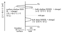
도 1은 산화물 반도체층 내부, 및 이의 계면 근방의 DOS를 나타낸 밴드 구조.
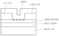
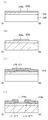
도 2는 산화물 반도체층을 갖는 트랜지스터의 단면 모식도.
도 3은 암(暗) 상태에서의 산화물 반도체층을 갖는 트랜지스터의 열화를 설명한 도면.
도 4는 암 상태에서의 산화물 반도체층을 갖는 트랜지스터의 열화를 설명한 도면.
도 5는 광 조사하에서의 산화물 반도체층을 갖는 트랜지스터의 열화를 설명한 도면.
도 6은 광 조사하에서의 산화물 반도체층을 갖는 트랜지스터의 열화를 설명한 도면.
도 7은 광 조사하에서의 산화물 반도체층을 갖는 트랜지스터의 열화를 설명한 도면.
도 8은 산화물 반도체층의 고순도 진성화를 설명한 모델 도면.
도 9는 트랜지스터의 단면도 및 등가 회로를 도시한 도면.
도 10은 밴드 구조를 나타낸 도면.
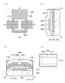
도 11은 본 발명의 일 형태에 따른 트랜지스터의 일례를 도시한 상면도 및 단면도.
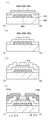
도 12는 본 발명의 일 형태에 따른 트랜지스터의 소스 전극 및 드레인 전극 근방의 단면의 일례를 도시한 도면.
도 13은 본 발명의 일 형태에 따른 트랜지스터의 제작 방법의 일례를 도시한 단면도.
도 14는 본 발명의 일 형태에 따른 트랜지스터의 제작 방법의 일례를 도시한 단면도.
도 15는 본 발명의 일 형태에 따른 트랜지스터의 일례를 도시한 상면도 및 단면도.
도 16은 본 발명의 일 형태에 따른 트랜지스터의 제작 방법의 일례를 도시한 단면도.
도 17은 본 발명의 일 형태에 따른 트랜지스터의 제작 방법의 일례를 도시한 단면도.
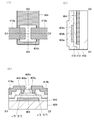
도 18은 본 발명의 일 형태에 따른 트랜지스터의 일례를 도시한 상면도 및 단면도.
도 19는 본 발명의 일 형태에 따른 트랜지스터의 제작 방법의 일례를 도시한 단면도.
도 20은 본 발명의 일 형태에 따른 트랜지스터의 일례를 도시한 상면도 및 단면도.
도 21은 본 발명의 일 형태에 따른 트랜지스터의 제작 방법의 일례를 도시한 단면도.
도 22는 본 발명의 일 형태에 따른 산화물 적층의 밴드 구조를 설명한 도면.
도 23은 산화물 반도체의 나노 빔 전자선 회절 패턴을 도시한 도면.
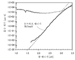
도 24는 CPM에 의하여 측정된 흡수 계수를 나타낸 도면.
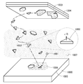
도 25는 타깃으로부터 박리된 스퍼터링 입자가 피성막면에 도달하는 태양(態樣)을 도시한 모식도.
도 26은 타깃으로부터 박리된 스퍼터링 입자가 피성막면에 도달하는 태양을 도시한 모식도.
도 27은 InGaO3(ZnO)m(m은 자연수)으로 표기되는 동족 화합물의 m=1인 경우의 결정 구조를 나타낸 도면.
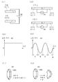
도 28은 DC전원, AC전원을 사용한 스퍼터링법에 의한 플라즈마 방전을 설명한 도면.
도 29는 스퍼터링 입자가 피성막면에 도달하는 태양을 도시한 모식도.
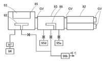
도 30은 성막 장치의 일례를 도시한 상면도.
도 31은 성막실의 일례를 도시한 단면도.
도 32는 가열 처리실의 일례를 도시한 도면.
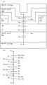
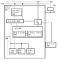
도 33은 본 발명의 일 형태에 따른 반도체 장치의 일례를 도시한 블록도.
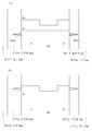
도 34는 본 발명의 일 형태에 따른 반도체 장치의 일례를 도시한 단면도 및 회로도.
도 35는 본 발명의 일 형태에 따른 CPU의 일례를 도시한 블록도.
도 36은 본 발명의 일 형태에 따른 전자 기기의 일례를 도시한 도면.
도 37은 본 발명의 일 형태에 따른 EL 표시 장치의 일례를 도시한 회로도, 상면도, 및 단면도.
도 38은 본 발명의 일 형태에 따른 액정 표시 장치의 일례를 도시한 회로도 및 단면도.BRIEF DESCRIPTION OF THE DRAWINGS Fig. 1 is a band structure showing the inside of the oxide semiconductor layer and the DOS in the vicinity of the interface thereof.
2 is a cross-sectional schematic diagram of a transistor having an oxide semiconductor layer.
3 is a view for explaining deterioration of a transistor having an oxide semiconductor layer in a dark state;
4 is a view for explaining deterioration of a transistor having an oxide semiconductor layer in a dark state;
5 is a view for explaining deterioration of a transistor having an oxide semiconductor layer under light irradiation;
6 is a view for explaining deterioration of a transistor having an oxide semiconductor layer under light irradiation;
7 is a diagram for explaining deterioration of a transistor having an oxide semiconductor layer under light irradiation;
8 is a model drawing illustrating high purity crystallization of an oxide semiconductor layer.
9 is a sectional view and equivalent circuit of a transistor.
10 shows a band structure.
11 is a top view and a cross-sectional view showing an example of a transistor according to an embodiment of the present invention.
12 is a view showing an example of a cross section in the vicinity of a source electrode and a drain electrode of a transistor according to an embodiment of the present invention;
13 is a sectional view showing an example of a method of manufacturing a transistor according to an embodiment of the present invention.
14 is a cross-sectional view showing an example of a method of manufacturing a transistor according to an embodiment of the present invention.
15 is a top view and a cross-sectional view showing an example of a transistor according to an embodiment of the present invention;
16 is a sectional view showing an example of a method of manufacturing a transistor according to an embodiment of the present invention.
17 is a sectional view showing an example of a method of manufacturing a transistor according to an embodiment of the present invention.
18 is a top view and a cross-sectional view showing an example of a transistor according to an embodiment of the present invention;
19 is a cross-sectional view showing an example of a method of manufacturing a transistor according to an embodiment of the present invention.
20 is a top view and a cross-sectional view showing an example of a transistor according to an embodiment of the present invention;
21 is a cross-sectional view showing an example of a method of manufacturing a transistor according to an embodiment of the present invention.
22 is a view for explaining a band structure of an oxide laminate according to an embodiment of the present invention.
23 is a view showing a nano-beam electron beam diffraction pattern of an oxide semiconductor.
24 shows absorption coefficients measured by CPM;
25 is a schematic diagram showing a state in which sputtering particles peeled off from a target reaches a surface to be coated;
26 is a schematic diagram showing a state in which sputtering particles peeled from the target reach the surface to be coated;
27 is a diagram showing a crystal structure when m = 1 of a homologue compound represented by InGaO 3 (ZnO) m (m is a natural number);
28 is a view for explaining a plasma discharge by a sputtering method using a DC power source and an AC power source.
29 is a schematic diagram showing a state in which sputtering particles reach the surface to be film-formed;
30 is a top view showing an example of a film forming apparatus.
31 is a sectional view showing an example of a deposition chamber;
32 is a view showing an example of a heat treatment chamber;
33 is a block diagram showing an example of a semiconductor device according to an embodiment of the present invention;
34 is a cross-sectional view and a circuit diagram showing an example of a semiconductor device according to an embodiment of the present invention;
35 is a block diagram showing an example of a CPU according to an embodiment of the present invention;
36 is a view showing an example of an electronic apparatus according to an embodiment of the present invention;
37 is a circuit diagram, a top view, and a cross-sectional view showing an example of an EL display device according to an embodiment of the present invention;
38 is a circuit diagram and a sectional view showing an example of a liquid crystal display device according to an embodiment of the present invention;
본 발명의 실시형태에 대하여 도면을 사용하여 자세히 설명하기로 한다. 그러나, 본 발명은 하기의 설명에 제한되지 않고 그 형태 및 자세한 사항을 다양하게 변경할 수 있는 것은 당업자라면 용이하게 이해할 수 있다. 또한, 본 발명은 하기의 실시형태의 기재 내용에 제한되어 해석되는 것이 아니다. 또한, 도면을 사용하여 발명의 구성을 설명하는 데 있어서, 동일한 것을 가리키는 부호는 다른 도면간에서도 공통으로 사용된다. 또한, 동일한 것을 가리킬 때에는 해치 패턴을 동일하게 하고, 부호를 특별히 붙이지 않는 경우가 있다.DESCRIPTION OF THE PREFERRED EMBODIMENTS Embodiments of the present invention will be described in detail with reference to the drawings. However, it is to be understood that the present invention is not limited to the following description, and various changes in the form and details may be readily apparent to those skilled in the art. Furthermore, the present invention is not construed as being limited to the description of the following embodiments. In describing the constitution of the invention using the drawings, the same reference numerals are used in common between different drawings. Further, when the same thing is indicated, the hatch pattern may be made the same, and the sign may not be specified.
또한, 어느 하나의 실시형태 중에서 설명하는 내용(일부의 내용이어도 좋음)은, 이의 실시형태에서 설명하는 다른 내용(일부의 내용이어도 좋음)에 대하여, 적용, 조합, 또는 치환 등을 수행할 수 있다.In addition, the contents (some contents may be) described in any one of the embodiments may be applied, combined, substituted, or the like to other contents described in the embodiments (or a part thereof) .
또한, 도면에 있어서, 크기, 층의 두께, 또는 영역은, 명료화를 위하여 과장되는 경우가 있다. 따라서, 그 스케일에 반드시 한정되지 않는다.Further, in the drawings, the size, the layer thickness, or the area may be exaggerated for clarity. Therefore, it is not necessarily limited to the scale.
또한, 도면은 이상(理想)적인 예를 모식적으로 도시한 것이며, 도시된 형상 또는 값 등에 제한되지 않는다. 예를 들어, 제조 기술에 따라 생기는 형상의 편차, 오차로 인한 형상의 편차, 노이즈에 기인하는 신호, 전압, 또는 전류의 편차, 또는 타이밍의 어긋남으로 인한 신호, 전압, 또는 전류의 편차 등이 포함될 수 있다.In addition, the drawings are diagrammatic representations of ideal examples, and are not limited to the shapes or values shown and the like. For example, a deviation of a shape caused by a manufacturing technique, a deviation of a shape due to an error, a deviation of a signal, a voltage, or a current due to noise, or a deviation of a signal, a voltage, or a current due to a shift in timing .
또한, 전압이란 어느 전위와 기준 전위(예를 들어, 접지 전위(GND) 또는 소스 전위)와의 전위차를 말하는 경우가 많다. 따라서, 전압을 전위로 바꾸어 말할 수 있다.The voltage is often referred to as a potential difference between a certain potential and a reference potential (for example, ground potential (GND) or source potential). Therefore, the voltage can be said to be a potential.
본 명세서 중에서는 "전기적으로 접속된다"라고 표현된 경우에도, 현실의 회로에서는 물리적인 접속 부분이 없고 그저 배선이 연장되어 있을 뿐인 경우도 있다.In the present specification, even when expressed as "electrically connected ", there is no physical connection portion in a real circuit, and there is a case where the wiring is simply extended.
또한, 제1, 제2로서 부여되는 서수사는 편의상 사용되는 것이며, 공정 순서 또는 적층 순서를 나타내는 것이 아니다. 또한, 본 명세서에 있어서 발명을 특정하기 위한 사항으로서 고유의 명칭을 나타내는 것이 아니다.The ordinal numbers assigned as the first and second are used for convenience, and do not indicate a process order or a stacking order. In addition, in the present specification, names specific to the invention are not indicated.
본 명세서 중에 있어서, 예를 들어 물체의 형상을 "직경", "입경", "크기(dimension)", "사이즈(size)", "폭" 등으로 규정하는 경우, 물체가 들어가는 최소의 입방체에서의 한 변의 길이, 또는 물체의 한 단면에서의 원상당 직경으로 바꿔 읽어도 좋다. 물체의 한 단면에서의 원상당 직경이란, 물체의 한 단면과 동등한 면적을 갖는 정원의 직경을 말한다.In the present specification, for example, when the shape of an object is defined by "diameter", "particle size", "size", "size", "width", etc., the minimum cube The diameter of one side of the object, or the circle-equivalent diameter of one side of the object. The circle equivalent diameter in one cross section of an object means the diameter of a garden having an area equal to one cross section of the object.
또한, "반도체"라고 표기한 경우에도 예를 들어 도전성이 충분히 낮은 경우에는 "절연체"로서의 특성을 갖는 경우가 있다. 또한, "반도체"와 "절연체"는 경계가 애매하며 엄밀하게 구별할 수 없는 경우가 있다. 따라서, 본 명세서에 기재된 "반도체"는 "절연체"로 바꿔 말할 수 있는 경우가 있다. 마찬가지로, 본 명세서에 기재된 "절연체"는 "반도체"로 바꿔 말할 수 있는 경우가 있다.Further, even when the word "semiconductor" is written, for example, when the conductivity is sufficiently low, there is a case where the semiconductor device has characteristics as an "insulator ". Further, there is a case where the semiconductor and the insulator are vague and can not be distinguished precisely. Thus, the term " semiconductor "described herein may be referred to as an" insulator ". Likewise, the term "insulator" described herein may be referred to as "semiconductor ".
또한, "반도체"라고 표기한 경우에도 예를 들어 도전성이 충분히 높은 경우에는 "도전체"로서의 특성을 갖는 경우가 있다. 또한, "반도체"와 "도전체"는 경계가 애매하며 엄밀하게 구별할 수 없는 경우가 있다. 따라서, 본 명세서에 기재된 "반도체"는 "도전체"로 바꿔 말할 수 있는 경우가 있다. 마찬가지로, 본 명세서에 기재된 "도전체"는 "반도체"로 바꿔 말할 수 있는 경우가 있다.In the case where the word "semiconductor" is used, for example, when the conductivity is sufficiently high, there may be a case where the semiconductor device has characteristics as a "conductor ". In addition, "semiconductor" and "conductor" are vague and can not be strictly distinguished from each other. Thus, the term " semiconductor "as used herein may be referred to as" conductor ". Likewise, "conductors" described herein may be referred to as "semiconductors ".
또한, 반도체층의 불순물이란, 예를 들어 반도체층을 구성하는 주성분 이외를 말한다. 예를 들어, 농도가 0.1atomic% 미만의 원소는 불순물이다. 불순물이 포함되면, 예를 들어 반도체층의 DOS(Density of State)가 높게 되거나, 캐리어 이동도가 저하되거나, 결정성이 저하되는 경우 등이 있다. 반도체층이 산화물 반도체층인 경우, 반도체층의 특성을 변화시키는 불순물로서는, 예를 들어 제1족 원소, 제2족 원소, 제14족 원소, 제15족 원소, 주성분 이외의 천이 금속 등이 있고, 특히 예를 들어 수소(물도 포함됨), 리튬, 나트륨, 실리콘, 붕소, 인, 탄소, 질소 등이 있다. 산화물 반도체는, 불순물의 혼입으로 인하여 산소 결손을 형성하는 경우가 있다. 또한, 반도체층이 실리콘층인 경우, 반도체층의 특성을 변화시키는 불순물로서는, 예를 들어, 산소, 수소를 제외하는 제1족 원소, 제2족 원소, 제13족 원소, 제15족 원소 등이 있다.The impurity of the semiconductor layer refers to, for example, other than the main component constituting the semiconductor layer. For example, an element with a concentration of less than 0.1 atomic% is an impurity. When impurities are included, for example, the DOS (Density of State) of the semiconductor layer is increased, the carrier mobility is decreased, or the crystallinity is lowered. In the case where the semiconductor layer is an oxide semiconductor layer, examples of the impurity which changes the characteristics of the semiconductor layer include a
<산화물 반도체층에서의 DOS, 및 DOS를 만드는 원인 원소의 관계를 설명하기 위한 모델>≪ Model for explaining the relationship between the DOS in the oxide semiconductor layer and the causative element for making DOS >
산화물 반도체층 내부, 및 산화물 반도체층과 외부의 계면 근방에서 DOS(Density of State)가 존재하면, 산화물 반도체층을 갖는 트랜지스터의 열화 등의 원인이 된다. 산화물 반도체층 내부, 및 이의 계면 근방의 DOS에 대해서는 산소(O), 산소 결손(Vo), 및 수소(H)의 위치나 결합 관계에 따라 설명할 수 있다. 이하에서, 본 발명의 모델의 개요를 특성 이해를 위하여 설명하기로 한다.The presence of DOS (Density of State) in the oxide semiconductor layer and in the vicinity of the interface with the oxide semiconductor layer causes deterioration of the transistor including the oxide semiconductor layer. The inside of the oxide semiconductor layer and the DOS in the vicinity of the interface thereof can be explained by the positions of oxygen (O), oxygen vacancies (Vo), and the positions and bonding relationships of hydrogen (H). Hereinafter, the outline of the model of the present invention will be described for the sake of understanding the characteristics.
결론부터 말하자면, 트랜지스터에 안정적인 전기 특성을 부여하기 위해서는 산화물 반도체층 내부, 및 이의 계면 근방의 DOS를 더 저감시키는 것(고순도 진성화)이 중요하다. 이 DOS를 저감시키기 위해서는, 산소 결손 및 수소를 저감시킬 필요가 있다. 이하에서, 산화물 반도체층 내부, 및 이의 계면 근방의 DOS에 관하여 산소 결손 및 수소를 저감시킬 필요가 왜 있느냐에 대하여 모델을 사용하면서 설명하기로 한다.From the conclusion, in order to impart stable electric characteristics to the transistor, it is important to further reduce the DOS in the oxide semiconductor layer and its vicinity (high purity). In order to reduce this DOS, it is necessary to reduce oxygen deficiency and hydrogen. Hereinafter, a description will be given using a model as to why there is a need to reduce oxygen deficiency and hydrogen with respect to the inside of the oxide semiconductor layer and the DOS in the vicinity of the interface therebetween.
도 1은 산화물 반도체층 내부, 및 이의 계면 근방의 DOS를 나타낸 밴드 구조이다. 이하에서는, 산화물 반도체층이 인듐, 갈륨, 및 아연을 갖는 산화물 반도체층인 경우에 대하여 설명하기로 한다.1 shows a band structure inside the oxide semiconductor layer and DOS near the interface thereof. Hereinafter, the case where the oxide semiconductor layer is an oxide semiconductor layer having indium, gallium, and zinc will be described.
우선, 일반적으로 DOS에는 얕은 위치의 DOS(shallow level DOS)와 깊은 위치의 DOS(deep level DOS)가 있다. 또한, 본 명세서 중에 있어서 얕은 위치의 DOS는 전도대 하단의 에너지(Ec)와 중간 갭(mid gap) 사이의 DOS를 말한다. 따라서, 예를 들어 얕은 위치의 DOS는 전도대 하단의 에너지 부근에 위치한다. 또한, 본 명세서 중에 있어서, 깊은 위치의 DOS는 가전자대 상단의 에너지(Ev)와 중간 갭 사이의 DOS를 말한다. 따라서, 예를 들어 깊은 위치의 DOS는 가전자대 상단의 에너지보다 중간 갭 부근에 위치한다.First, DOS generally has shallow DOS (shallow level DOS) and deep DOS (deep DOS). Also, in this specification, the DOS in the shallow position refers to the DOS between the energy (Ec) at the lower end of the conduction band and the mid gap. Thus, for example, the DOS in a shallow position is located near the energy of the bottom of the conduction band. Also, in the present specification, DOS at a deep position refers to DOS between the energy (Ev) at the top of the valence band and the middle gap. Thus, for example, the DOS at a deep position is located near the mid-gap than the energy at the top of the valence band.
얕은 위치의 DOS에는 두 가지가 있다. 하나의 얕은 위치의 DOS는, 산화물 반도체층의 표면 근방(절연막(Insulator)과의 계면 또는 이의 근방)의 DOS(surface shallow DOS)이다. 다른 하나의 얕은 위치의 DOS는 산화물 반도체층 내부의 DOS(bulk shallow DOS)이다. 한편, 깊은 위치의 DOS로서는, 산화물 반도체층 내부의 DOS(bulk deep DOS)가 있다.DOS in shallow position has two kinds. DOS at one shallow position is a DOS (surface shallow DOS) near the surface of the oxide semiconductor layer (the interface with the insulator or the vicinity thereof). The DOS in the other shallow position is DOS (bulk shallow DOS) inside the oxide semiconductor layer. On the other hand, as the DOS in the deep position, DOS (bulk deep DOS) inside the oxide semiconductor layer exists.
이들 DOS는, 다음에 제시하는 바와 같이 작용할 가능성이 있다. 우선, 산화물 반도체층의 표면 근방의 surface shallow DOS는 전도대 하단으로부터 얕은 위치에 있으므로, 전하의 포획 및 소실이 일어나기 쉽다. 다음으로, 산화물 반도체층 내부의 bulk shallow DOS는 산화물 반도체층의 표면 근방의 surface shallow DOS에 비하여 전도대 하단으로부터 깊은 위치에 있으므로, 전하의 소실이 일어나기 어렵다.These DOS are likely to act as suggested below. First, the surface shallow DOS in the vicinity of the surface of the oxide semiconductor layer is located at a shallow position from the lower end of the conduction band, so that charge trapping and loss are likely to occur. Next, the bulk shallow DOS in the oxide semiconductor layer is located deep from the bottom of the conduction band, compared with the surface shallow DOS in the vicinity of the surface of the oxide semiconductor layer, so that the charge is hardly lost.
이하에서는, 산화물 반도체층에 DOS를 만드는 원인 원소에 대하여 설명하기로 한다.Hereinafter, the element causing the DOS in the oxide semiconductor layer will be described.
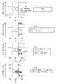
예를 들어, 산화물 반도체층 위에 산화 실리콘막을 형성하는 경우, 산화물 반도체층에 포함되는 인듐이 산화 실리콘막 내에 들어가 실리콘과 치환됨으로써, 얕은 위치의 DOS를 만드는 경우가 있다.For example, when a silicon oxide film is formed on the oxide semiconductor layer, indium contained in the oxide semiconductor layer enters the silicon oxide film and is replaced with silicon, thereby making a shallow DOS.
또한, 예를 들어 산화물 반도체층과 산화 실리콘막의 계면에서는, 산화물 반도체층에 포함되는 인듐과 산소의 결합이 끊어져 이 산소와 실리콘의 결합이 생긴다. 이것은, 실리콘과 산소의 결합 에너지가 인듐과 산소의 결합 에너지보다 높은 것, 및 실리콘(4가)이 인듐(3가)보다 원자가가 높은 것에 기인하다. 그리고 산화물 반도체층에 포함되는 산소가 실리콘에 의하여 빼앗겨, 인듐과 결합되어 있던 산소의 사이트(site)는 산소 결손이 된다. 또한, 이 현상은 표면에서뿐만 아니라, 산화물 반도체층 내부에 실리콘이 들어간 경우에도 마찬가지로 일어난다. 이들 산소 결손은 깊은 위치의 DOS를 형성한다.Further, for example, at the interface between the oxide semiconductor layer and the silicon oxide film, the bond of indium and oxygen contained in the oxide semiconductor layer is broken, and the bond of oxygen and silicon is generated. This is because the bonding energy between silicon and oxygen is higher than the bonding energy between indium and oxygen, and that silicon (tetravalent) is higher in valence than indium (trivalent). The oxygen contained in the oxide semiconductor layer is removed by the silicon, and the site of the oxygen bonded to the indium becomes oxygen deficiency. This phenomenon occurs not only on the surface but also when the silicon is introduced into the oxide semiconductor layer. These oxygen defects form DOS in deep position.
또한, 실리콘뿐만 아니라 다른 요인으로 인하여 인듐과 산소의 결합이 끊어질 수 있다. 예를 들어, 인듐, 갈륨, 및 아연을 갖는 산화물 반도체층에 있어서, 인듐과 산소의 결합은 갈륨 또는 아연과 산소의 결합보다 약해서 끊어지기 쉽다. 그러므로, 예를 들어 플라즈마로 인한 대미지나 스퍼터링 입자로 인한 대미지 등에 따라 인듐과 산소의 결합이 끊어져 산소 결손이 생길 수도 있다. 이 산소 결손은 깊은 위치의 DOS를 형성한다. 이 깊은 위치의 DOS는 정공을 포획할 수 있으므로 정공 트랩(정공 포획 중심)이 된다. 즉, 이 산소 결손이 산화물 반도체층 내부의 bulk deep DOS를 형성한다.Furthermore, due to other factors as well as silicon, the bond between indium and oxygen can be broken. For example, in an oxide semiconductor layer having indium, gallium, and zinc, a bond of indium and oxygen is weaker than a bond of gallium or zinc and oxygen, and is likely to be broken. Therefore, for example, due to the damage caused by the plasma or the sputtering particles due to the plasma, the bond between indium and oxygen may be broken and oxygen deficiency may occur. This oxygen deficiency forms a deep position DOS. DOS in this deep position can trap holes, and therefore, it becomes a hole trap (hole capture center). That is, this oxygen deficiency forms a bulk deep DOS in the oxide semiconductor layer.
이 산소 결손으로 인하여 형성된 깊은 위치의 DOS는, 나중에 설명하는 바와 같이, 수소가 원인이 되어 산화물 반도체층의 표면 근방의 surface shallow DOS나, 산화물 반도체층 내부의 bulk shallow DOS를 형성하는 요인 중 하나가 된다.The DOS in the deep position formed due to this oxygen deficiency is one of the factors causing hydrogen to cause the surface shallow DOS near the surface of the oxide semiconductor layer or the bulk shallow DOS inside the oxide semiconductor layer do.
이 산소 결손은 DOS를 형성하기 때문에 산화물 반도체층의 불안정 요인이 된다. 또한, 산화물 반도체층 내의 산소 결손은, 수소를 포획함으로써 준안정 상태가 된다. 즉, 깊은 위치의 DOS이며 정공을 포획할 수 있는 정공 트랩인 산소 결손이 수소를 포획하면, 얕은 위치의 DOS를 형성한다. 결과적으로 얕은 위치의 DOS는 전자를 포획할 수 있는 전자 트랩이 되거나, 전자의 발생원이 될 수 있다. 이와 같이 산소 결손은 수소를 포획한다. 그러나, 나중에 설명하는 바와 같이, 산화물 반도체층 내의 수소의 위치에 따라서는, 양(중성 또는 양)으로도 음(중성 또는 음)으로도 대전될 수 있다. 그러므로, 수소는 산화물 반도체층을 갖는 트랜지스터에 대하여 나쁜 영향을 미칠 가능성이 있다.This oxygen deficiency forms DOS, which is a factor of instability of the oxide semiconductor layer. Further, the oxygen deficiency in the oxide semiconductor layer becomes a metastable state by capturing hydrogen. In other words, if oxygen deficiency, which is a deep hole DOS and hole trap capable of trapping holes, captures hydrogen, a shallow DOS is formed. As a result, the DOS in the shallow position can be an electron trap capable of capturing electrons, or a source of electrons. Thus, the oxygen deficit captures hydrogen. However, as will be described later, depending on the position of hydrogen in the oxide semiconductor layer, either positive (neutral or positive) or negative (negative or negative) may be charged. Therefore, hydrogen may have a bad influence on a transistor having an oxide semiconductor layer.
일례로서, 도 2에 보텀 게이트 톱 콘택트 구조의 트랜지스터의 단면 모식도를 도시하였다. 산화물 반도체층(OS)은 절연막과의 계면 근방에 surface shallow DOS를 갖는다. surface shallow DOS에는 전자가 포획되어 있어 DOS는 음으로 대전되어 있다. 그러므로, surface shallow DOS는 트랜지스터의 문턱 전압을 변화시키는 요인이 된다.As an example, FIG. 2 shows a schematic cross-sectional view of the transistor of the bottom gate top contact structure. The oxide semiconductor layer (OS) has a surface shallow DOS in the vicinity of the interface with the insulating film. surface shallow DOS has electrons trapped and DOS is negatively charged. Therefore, the surface shallow DOS is a factor that changes the threshold voltage of the transistor.
그래서, 산소 결손이 트랜지스터에 대하여 나쁜 영향을 미치지 않도록 하기 위해서는 산소 결손의 밀도를 저감시키는 것이 중요하다. 산화물 반도체층에 과잉 산소를 공급함으로써, 즉, 산소 결손을 과잉 산소로 매립함으로써, 산화물 반도체층의 산소 결손의 밀도를 저감시킬 수 있다. 즉, 산소 결손은 과잉 산소가 들어가면 안정 상태가 된다. 예를 들어, 산화물 반도체층 내부 또는 산화물 반도체층의 계면 근방에 제공된 절연막 내에 과잉 산소를 갖게 한다. 그러면, 이 과잉 산소가 산화물 반도체층의 산소 결손을 매립함으로써 산화물 반도체층의 산소 결손을 효과적으로 소멸 또는 저감시킬 수 있다.Therefore, in order to prevent the oxygen deficiency from adversely affecting the transistor, it is important to reduce the density of the oxygen deficiency. The density of oxygen vacancies in the oxide semiconductor layer can be reduced by supplying excess oxygen to the oxide semiconductor layer, that is, by filling the oxygen vacancies with excess oxygen. That is, oxygen deficiency becomes stable when excess oxygen enters. For example, the insulating film provided in the oxide semiconductor layer or near the interface of the oxide semiconductor layer has excess oxygen. Then, this excess oxygen buries the oxygen vacancy in the oxide semiconductor layer, so that the oxygen vacancy in the oxide semiconductor layer can be effectively eliminated or reduced.
여기서, 과잉 산소란 예를 들어 화학양론적 조성을 넘어서 포함되는 산소를 말한다. 또는, 과잉 산소란 예를 들어 가열 처리를 수행함으로써 방출되는 산소를 말한다. 과잉 산소는, 예를 들어 막이나 층의 내부를 이동할 수 있다. 과잉 산소의 이동에는, 막이나 층의 원자간을 이동하는 경우와, 당구 공과 같이 막이나 층을 구성하는 산소와 서로 바뀌면서 이동하는 경우가 있다. 또한, 산화물 반도체층 내에서, 산소 결손은 인접되는 산소 원자를 잇달아 포획함으로써 이동하는 경우가 있다.Here, the term " excess oxygen " refers to oxygen contained, for example, beyond the stoichiometric composition. Alternatively, the excess oxygen refers to oxygen released by, for example, performing a heat treatment. Excess oxygen can, for example, move inside the membrane or layer. Excess oxygen may migrate between atoms of a film or a layer and oxygen, such as a billiard ball, exchanging with oxygen constituting the film or layer. Further, in the oxide semiconductor layer, the oxygen deficiency may move by capturing successive oxygen atoms successively.
상술한 바와 같이, 산소 결손은 수소 또는 산소 중 어느 쪽에 따라 준안정 상태 또는 안정 상태가 된다. 산화물 반도체층 내의 수소 농도가 높은 경우, 수소를 포획하는 산소 결손이 많게 된다. 한편, 산소 결손 내에 수소가 존재하는 경우, 과잉 산소를 공급하여도 과잉 산소는 우선, 수소를 제거하기 위하여 사용된다. 그러므로 과잉 산소는, 수소를 제거한 후에야 산소 결손을 겨우 매립하기 위하여 사용된다. 따라서, 산화물 반도체층 내의 수소 농도가 높은 경우, 과잉 산소에 의하여 저감시킬 수 있는 산소 결손이 적게 된다. 이와 반대로, 산화물 반도체층 내의 수소 농도가 낮은 경우, 산소 결손에 포획되는 수소가 적게 된다. 그러므로, 과잉 산소를 공급함으로써 산소 결손의 밀도를 대폭적으로 저감시킬 수 있다.As described above, the oxygen deficiency becomes a metastable state or a stable state depending on either hydrogen or oxygen. When the concentration of hydrogen in the oxide semiconductor layer is high, oxygen deficiency that captures hydrogen becomes large. On the other hand, when hydrogen exists in the oxygen deficiency, excess oxygen is first used to remove hydrogen even when excess oxygen is supplied. Therefore, the excess oxygen is used only to fill the oxygen deficit after removing the hydrogen. Therefore, when the hydrogen concentration in the oxide semiconductor layer is high, the oxygen deficiency that can be reduced by the excess oxygen becomes small. On the other hand, when the concentration of hydrogen in the oxide semiconductor layer is low, the amount of hydrogen trapped in the oxygen deficiency is small. Therefore, the density of oxygen deficiency can be greatly reduced by supplying excess oxygen.
상술한 바와 같이, 산소 결손은 수소를 포획하지만, 수소의 포획 방법에 따라서는 양(중성 또는 양)으로도 음(중성 또는 음)으로도 대전될 수 있다. 여기서는, 산화물 반도체층 내부의 bulk shallow DOS와, 표면 근방의 surface shallow DOS에 대하여 생각한다. 이들 shallow level DOS가 중성 또는 음으로 대전되거나, 중성 또는 양으로 대전되는 것은, 수소(수소 결합), 산소 결손 및 산소의 상대적인 위치를 생각하기만 하면 이해할 수 있다. 예를 들어, 산화물 반도체층 내부에서, 수소가 산소 결손에 의하여 포획되고 VoH가 형성되면 중성 또는 양으로 대전된다. 즉, H++e-가 산화물 반도체층 내부의 bulk shallow DOS를 형성하고, 산화물 반도체층에 n형 영역을 형성하는 요인이 된다.As described above, the oxygen deficit captures hydrogen but may be negatively charged (neutral or negative) depending on the capturing method of hydrogen (neutral or positive). Here, bulk shallow DOS in the oxide semiconductor layer and surface shallow DOS in the vicinity of the surface are considered. These shallow-level DOSs are neutral or negatively charged, neutral or positively charged if only the relative positions of hydrogen (hydrogen bond), oxygen deficiency, and oxygen are considered. For example, in the oxide semiconductor layer, when hydrogen is trapped by the oxygen vacancy and VoH is formed, it is neutralized or positively charged. That is, H + + e - forms a bulk shallow DOS in the oxide semiconductor layer and forms an n-type region in the oxide semiconductor layer.
한편, 수소는 중성 또는 양으로 대전될 뿐만 아니라, 중성 또는 음으로 대전되는 경우도 있다. 이것을 고려하면, 산화물 반도체층 내부의 bulk shallow DOS와, 산화물 반도체층 표면 근방의 surface shallow DOS를 형성하는 바와 같은 이하에 제시되는 모델이 생각된다. 또한, 모델의 "…"는 결합을 나타내는 것은 아니다. 또한, 모델의 "…"는, 원자간의 이온성 결합을 나타내는 모델의 "-"와 구별하기 위하여 사용된다.On the other hand, hydrogen may be neutral or positively charged as well as neutral or negatively charged. Considering this, a bulk shallow DOS in the oxide semiconductor layer and a surface shallow DOS in the vicinity of the surface of the oxide semiconductor layer are considered, as shown below. Also, the "..." of the model does not indicate a combination. Also, "..." in the model is used to distinguish it from "-" in the model that represents ionic bonds between atoms.
우선, 산화물 반도체층에 포함되는 인듐과 산소의 결합이 끊어져 이 산소와 실리콘의 결합이 생기고, 또한 수소가 존재하는 경우에 대하여, 표 1에 모델을 열거한다.First, the model is listed in Table 1 for the case where the bond between indium and oxygen contained in the oxide semiconductor layer is broken and the oxygen is bonded to silicon and hydrogen is present.

예를 들어, 수소가 산소와 결합된 모델 A가 있다.For example, there is a model A in which hydrogen is combined with oxygen.
또한, 예를 들어 수소가 산소 결손에 포획된 모델 B가 있다.Also, for example, there is a model B in which hydrogen is trapped in an oxygen vacancy.
또한, 실리콘을 인듐으로 치환한 경우도 마찬가지이다. 예를 들어, 수소가 산소와 결합된 모델 C가 있다.This also applies to the case where silicon is replaced with indium. For example, there is a model C in which hydrogen is combined with oxygen.
또한, 예를 들어 수소가 산소 결손에 포획된 모델 D가 있다.Also, for example, there is a model D in which hydrogen is trapped in an oxygen vacancy.
이와 같이 4개의 모델 A 내지 모델 D가 생각된다. 이 모델에 의하여, 중성 또는 양뿐만 아니라, 중성 또는 음 중, 어느 쪽으로 대전되는 것을 설명할 수 있다. 다만, 인듐에 비하여 실리콘이 결합이 강하기 때문에, 모델 D에 비하여 모델 B의 가능성이 낮다고 생각된다.Thus, four models A to D are conceivable. According to this model, it can be explained that either neutral or negative, as well as neutral or negative, are charged. However, since the bond of silicon is stronger than that of indium, the possibility of model B is considered to be lower than that of model D.
따라서, 수소, 산소 결손 및 산소의 상대적인 위치 관계에 따라 수소는 양 및 음의 양쪽으로 대전될 가능성이 있다. 즉, 산소 결손과 수소는, 양으로 대전되는 DOS와 음으로 대전되는 DOS 양쪽을 형성할 수 있다. 이들은, 주위의 환경(주위에 배치되는 원소의 전기 음성도)에 따라 양 및 음 중 어느 쪽으로 대전될 수 있는 가능성이 있다.Therefore, depending on the relative positional relationship between hydrogen, oxygen deficiency, and oxygen, hydrogen may be charged in both positive and negative directions. That is, oxygen deficiency and hydrogen can form both positively charged DOS and negatively charged DOS. They are likely to be charged either positive or negative depending on the surrounding environment (electronegativity of the element disposed around).
<산화물 반도체층을 갖는 트랜지스터의 암 상태에서의 히스테리시스 열화 모델>≪ Hysteresis deterioration model in a dark state of a transistor having an oxide semiconductor layer >
다음에, 산화물 반도체층을 갖는 트랜지스터의 열화의 메커니즘에 대하여 설명하기로 한다. 산화물 반도체층을 갖는 트랜지스터는, 빛이 조사되어 있는 경우와 빛이 조사되어 있지 않은 경우에 따라 특성이 열화될 때의 거동이 다르다. 빛이 조사되어 있는 경우는, 산화물 반도체층 내부의 깊은 위치의 DOS(bulk deep DOS)가 크게 영향을 미칠 가능성이 있다. 빛이 조사되어 있지 않은 경우는, 산화물 반도체층의 표면 근방(절연막(Insulator)과의 계면 또는 이의 근방)의 얕은 위치의 DOS(surface shallow DOS)가 관계되고 있는 가능성이 있다.Next, the mechanism of deterioration of the transistor including the oxide semiconductor layer will be described. A transistor having an oxide semiconductor layer has a different behavior when characteristics are deteriorated depending on whether light is irradiated or not. When light is irradiated, there is a possibility that DOS (bulk deep DOS) at a deep position inside the oxide semiconductor layer greatly influences. If light is not irradiated, a DOS (surface shallow DOS) at a shallow position near the surface of the oxide semiconductor layer (at an interface with the insulator or in the vicinity thereof) may be involved.
그래서, 우선, 산화물 반도체층을 갖는 트랜지스터에 빛이 조사되어 있지 않은 경우(암 상태)에 대하여 설명하기로 한다. 이 경우는 산화물 반도체층의 표면 근방(절연막(Insulator)과의 계면 또는 이의 근방)의 얕은 위치의 DOS(surface shallow DOS)에 의한 전하의 포획, 방출의 관계로부터 트랜지스터의 열화 메커니즘을 설명할 수 있다.Therefore, first, the case where the transistor having the oxide semiconductor layer is not irradiated with light (dark state) will be described. In this case, the deterioration mechanism of the transistor can be explained from the relationship of charge capture and discharge by DOS (surface shallow DOS) at a shallow position near the surface of the oxide semiconductor layer (the interface with the insulator or the vicinity thereof) .
암 상태에서, 산화물 반도체층을 갖는 트랜지스터에 대하여 게이트 BT(bias temperature) 스트레스 시험을 번갈아 수행한 경우의 문턱 전압(Vth)의 변화를 도 3에 나타냈다. 도 3을 보면 알다시피, 플러스 게이트 BT 스트레스 시험(+GBT)을 수행함으로써 문턱 전압은 양 방향으로 변화된다. 다음에, 마이너스 게이트 BT 스트레스 시험(-GBT)을 수행하면 문턱 전압은 음 방향으로 변화되어 초기 값(Initial)과 같은 정도의 문턱 전압이 된다. 이와 같이 플러스 게이트 BT 스트레스 시험과 마이너스 게이트 BT 스트레스 시험을 교대로 반복하여 수행하면 문턱 전압이 상하로 변화된다(히스테리시스가 발생된다). 즉, 빛이 조사되어 있지 않은 상태에서 마이너스 게이트 BT 스트레스 시험과 플러스 게이트 BT 스트레스 시험을 번갈아 수행하면, 문턱 전압은 양 방향 및 음 방향으로 번갈아 변화되지만, 전체로서는 일정 범위 내에서의 변화에 그치는 것을 알았다.A change in the threshold voltage (Vth) when the gate BT (bias temperature) stress test is alternately performed for the transistor having the oxide semiconductor layer in the dark state is shown in Fig. As can be seen in FIG. 3, by performing the plus gate BT stress test (+ GBT), the threshold voltage changes in both directions. Next, when the negative gate BT stress test (-GBT) is performed, the threshold voltage changes in the negative direction and becomes the same threshold voltage as the initial value (Initial). When the positive gate BT stress test and the negative gate BT stress test are repeatedly performed in this manner, the threshold voltage changes up and down (hysteresis occurs). That is, when the negative gate BT stress test and the positive gate BT stress test are alternately performed in a state in which no light is irradiated, the threshold voltage alternately changes in both directions and negative direction, but as a whole, the change is within a certain range okay.
이와 같은 암 상태에서의 게이트 BT 스트레스 시험에 의한 트랜지스터의 문턱 전압의 변화는, 산화물 반도체층의 표면 근방의 surface shallow DOS에 의하여 설명할 수 있다. 도 4에는 산화물 반도체층을 포함한 밴드 구조와, 밴드 구조에 대응하는 플로 차트를 나타냈다. 또한, 여기서는, 빛이 조사되어 있지 않은 경우의 열화의 메커니즘에 대하여 생각하기 때문에, 게이트 BT 스트레스 시험을 수행하기 전에도, 게이트 BT 스트레스 시험을 수행하고 있는 동안에도, 게이트 BT 스트레스 시험을 수행한 후에도, 빛이 조사되어 있지 않은 경우에 대하여 설명하는 것으로 한다.The change of the threshold voltage of the transistor by the gate BT stress test in the dark state can be explained by the surface shallow DOS near the surface of the oxide semiconductor layer. 4 shows a band structure including an oxide semiconductor layer and a flow chart corresponding to a band structure. In addition, here, since the mechanism of deterioration in the case where no light is irradiated is considered, even before the gate BT stress test is performed, even after performing the gate BT stress test, and even after performing the gate BT stress test, The case where light is not irradiated will be described.
게이트 BT 스트레스를 인가하기 전(게이트 전압(Vg)은 0)에서는, 산화물 반도체층의 표면 근방의 surface shallow DOS는 페르미 준위(Ef)보다 에너지가 높고, 전자가 포획되어 있지 않기 때문에 전기적으로 중성이다(스텝 S101). 이 때, 측정한 문턱 전압을 게이트 BT 스트레스를 인가하기 전의 초기 값으로 한다.Before applying the gate BT stress (the gate voltage Vg is 0), the surface shallow DOS near the surface of the oxide semiconductor layer is higher in energy than the Fermi level Ef and electrons are neutral because electrons are not trapped (Step S101). At this time, the measured threshold voltage is set as an initial value before the gate BT stress is applied.
다음에 플러스 게이트 BT 스트레스 시험(암 상태)을 수행하고, 양의 게이트 전압을 인가한다. 양의 게이트 전압을 인가함으로써 전도대의 밴드가 구부러지고 산화물 반도체층의 표면 근방의 surface shallow DOS는 페르미 준위보다 에너지가 낮게 된다. 그러므로, 산화물 반도체층의 표면 근방의 surface shallow DOS에는 전자가 포획되어 DOS는 음으로 대전된다(스텝 S102).Next, a positive gate BT stress test (dark state) is performed, and a positive gate voltage is applied. By applying a positive gate voltage, the band of the conduction band is bent and the surface shallow DOS near the surface of the oxide semiconductor layer becomes lower in energy than the Fermi level. Therefore, electrons are trapped in the surface shallow DOS near the surface of the oxide semiconductor layer, and DOS is negatively charged (step S102).
다음에, 스트레스를 정지하고, 게이트 전압을 0으로 한다. 게이트 전압을 0으로 함으로써 산화물 반도체층의 표면 근방의 surface shallow DOS는 페르미 준위보다 에너지가 높게 된다. 그런데, 산화물 반도체층의 표면 근방의 surface shallow DOS에 포획된 전자가 방출될 때까지는 긴 시간이 걸린다. 그래서, 산화물 반도체층의 표면 근방의 surface shallow DOS는 음으로 대전된 상태가 유지된다(스텝 S103). 이 때, 트랜지스터의 채널 형성 영역에는 게이트 전압 외에도 음의 전압이 계속 인가되고 있는 상태이다. 따라서, 트랜지스터를 온 상태로 하기 위하여 초기 값보다 높은 게이트 전압을 인가해야 하고, 문턱 전압은 양 방향으로 변화된다. 즉, 노멀리오프(normally off)화되기 쉬워질 가능성이 있다.Next, the stress is stopped and the gate voltage is set to zero. By setting the gate voltage to zero, the surface shallow DOS near the surface of the oxide semiconductor layer becomes higher in energy than the Fermi level. However, it takes a long time until electrons trapped in the surface shallow DOS near the surface of the oxide semiconductor layer are emitted. Thus, the surface shallow DOS near the surface of the oxide semiconductor layer is maintained in the negatively charged state (step S103). At this time, in addition to the gate voltage, a negative voltage is continuously applied to the channel forming region of the transistor. Therefore, a gate voltage higher than the initial value must be applied to turn on the transistor, and the threshold voltage changes in both directions. That is, there is a possibility that it becomes easy to normally off.
다음에, 마이너스 게이트 BT 스트레스 시험(암 상태)을 수행하여, 음의 게이트 전압을 인가한다. 음의 게이트 전압을 인가함으로써 전도대의 밴드가 구부러지고 산화물 반도체층의 표면 근방의 surface shallow DOS는 더욱 높은 에너지가 된다. 그러므로, 산화물 반도체층의 표면 근방의 surface shallow DOS에 포획된 전자가 방출되어 DOS가 전기적으로 중성이 된다(스텝 S104). 이 전자의 방출에 기인하여, 문턱 전압이 게이트 BT 스트레스 시험을 수행하기 전의 초기 값과 대략 동등한 값으로 되돌아갈 가능성이 있다.Next, a negative gate BT stress test (dark state) is performed to apply a negative gate voltage. By applying a negative gate voltage, the band of the conduction band is bent and the surface shallow DOS near the surface of the oxide semiconductor layer becomes higher energy. Therefore, electrons trapped in the surface shallow DOS near the surface of the oxide semiconductor layer are released, and DOS becomes electrically neutral (step S104). Due to the emission of this electrons, there is a possibility that the threshold voltage returns to a value substantially equal to the initial value before the gate BT stress test is performed.
다음에, 스트레스를 정지하고, 게이트 전압을 0으로 한다. 이 때, 산화물 반도체층의 표면 근방의 surface shallow DOS는, 포획된 전자를 이미 방출한 것이므로, 전기적으로 중성이다(스텝 S101). 그러므로, 문턱 전압은 양 방향으로 변화되고, 결과적으로 게이트 BT 스트레스를 인가하기 전의 초기 값으로 되돌아간다. 즉, 빛이 조사되어 있지 않은 상태에서 마이너스 게이트 BT 스트레스 시험과 플러스 게이트 BT 스트레스 시험을 번갈아 수행하면 문턱 전압은 양 방향 및 음 방향으로 번갈아 변화된다. 그러나, 산화물 반도체층의 표면 근방의 surface shallow DOS에 있어서, 플러스 게이트 BT 스트레스 시험 시에 포획된 전자가 마이너스 게이트 BT 스트레스 시험 시에 방출되기 때문에 전체로서는 문턱 전압은 일정한 범위 내에서 변화되는 것을 알았다.Next, the stress is stopped and the gate voltage is set to zero. At this time, the surface shallow DOS in the vicinity of the surface of the oxide semiconductor layer is electrically neutral since it has already released trapped electrons (step S101). Therefore, the threshold voltage is changed in both directions and, as a result, returns to the initial value before applying the gate BT stress. That is, when the negative gate BT stress test and the positive gate BT stress test are alternately performed in the state that no light is irradiated, the threshold voltage alternately changes in both directions. However, in the surface shallow DOS near the surface of the oxide semiconductor layer, the electrons trapped in the positive gate BT stress test are released in the negative gate BT stress test, so that the threshold voltage as a whole changes within a certain range.
상기로부터, 암 상태에서의 게이트 BT 스트레스 시험에 의한 트랜지스터의 문턱 전압의 변화는 산화물 반도체층의 표면 근방의 surface shallow DOS를 이해함으로써 설명할 수 있다.From the above, the change of the threshold voltage of the transistor by the gate BT stress test in the dark state can be explained by understanding the surface shallow DOS near the surface of the oxide semiconductor layer.
<광 조사하에서의 산화물 반도체층을 갖는 트랜지스터의 열화 모델>≪ Degradation model of transistor having oxide semiconductor layer under light irradiation >
상술한 바와 같이, 산화물 반도체층을 갖는 트랜지스터의 열화는 빛이 조사되어 있는 경우와 빛이 조사되어 있지 않은 경우에 따라 거동이 다르다. 빛이 조사되어 있지 않은 경우에 대해서는 이미 설명하였다. 따라서, 여기서는 빛이 조사되어 있는 경우의 열화의 메커니즘에 대하여 설명하기로 한다. 빛이 조사되어 있는 경우는, 산화물 반도체층 내부의 깊은 위치의 DOS(bulk deep DOS)에 관계가 있다. 여기서는, 산화물 반도체층 내부의 깊은 위치의 DOS(bulk deep DOS)에 의한 전하의 포획, 방출의 관계로부터, 빛이 조사되어 있는 경우(명 상태)의 트랜지스터의 열화의 메커니즘을 설명하기로 한다.As described above, the deterioration of the transistor including the oxide semiconductor layer differs depending on the case where the light is irradiated and the case where the light is not irradiated. The case where the light is not irradiated has already been described. Therefore, the mechanism of deterioration in the case where light is irradiated will be described here. When light is irradiated, it is related to DOS (bulk deep DOS) at a deep position inside the oxide semiconductor layer. Here, the mechanism of deterioration of the transistor in the case where light is irradiated (light state) will be described from the relationship of trapping and discharging of charges due to DOS deep deep inside the oxide semiconductor layer.
도 5는 광 조사하에서 산화물 반도체층을 갖는 트랜지스터에 대하여 게이트 BT 스트레스 시험을 번갈아 수행한 경우의 문턱 전압(Vth)의 변화를 나타낸 것이다. 도 5를 보면 알다시피, 문턱 전압(Vth)은 초기 값(Initial)으로부터 변화된다.5 shows the change in the threshold voltage (Vth) when the gate BT stress test is alternately performed on the transistor having the oxide semiconductor layer under light irradiation. As can be seen in FIG. 5, the threshold voltage Vth changes from the initial value Initial.
도 5에서는, 먼저, 문턱 전압의 초기 값으로서, 게이트 BT 스트레스를 인가하지 않고 빛을 차광한 상태(암 상태)에서 측정한 결과를 플롯하였다. 다음에, 게이트 BT 스트레스를 인가하지 않고 빛을 조사한 상태(명 상태)에서 문턱 전압을 측정하였다. 결과적으로 빛을 차광한 상태(암 사태)에서의 문턱 전압에 비하여 빛을 조사한 상태(명 상태)에서의 문턱 전압은 음 방향으로 크게 변화되는 것을 알았다. 이것은, 빛을 조사함으로써 전자 및 정공(홀)이 생성되고, 생성된 전자가 전도대로 여기되기 때문일 수도 있다. 즉, 게이트 BT 스트레스를 인가하지 않는 경우에도 빛의 조사에 따라 산화물 반도체층을 갖는 트랜지스터의 문턱 전압은 음 방향으로 시프트되고 노멀리온화되기 쉬워진다고 할 수 있다. 이 경우, 산화물 반도체층의 에너지 갭이 클수록 또는 에너지 갭 내의 DOS가 적을수록, 여기되는 전자는 적게 된다. 그러므로, 이와 같은 경우에는 빛의 조사만에 기인한 문턱 전압의 변화는 작게 된다.In FIG. 5, first, as the initial value of the threshold voltage, a result obtained by measuring the light shielding state (dark state) without applying the gate BT stress was plotted. Next, the threshold voltage was measured in a state in which light was irradiated (light state) without application of the gate BT stress. As a result, it was found that the threshold voltage in the state (light state) in which the light was irradiated (light state) was significantly changed in the negative direction as compared with the threshold voltage in the light shielding state (cancer state). This may be because electrons and holes (holes) are generated by irradiating light, and generated electrons are excited to the conduction band. That is, even when the gate BT stress is not applied, the threshold voltage of the transistor having the oxide semiconductor layer is shifted in the negative direction and becomes easily normalized by light irradiation. In this case, the larger the energy gap of the oxide semiconductor layer or the smaller the DOS in the energy gap, the less electrons are excited. Therefore, in such a case, the change in the threshold voltage due to only irradiation of light is small.
다음에, 빛을 조사한 채 마이너스 게이트 BT 스트레스 시험(-GBT)을 수행하면 문턱 전압은 음 방향으로 더 변화되었다. 이것은, 산화물 반도체층 내부의 bulk deep DOS에 포획된 정공이 전계에 의하여 게이트 절연막(GI) 내의 비가교(非架橋) 산소 정공 포획 중심(NBOHC: Non Bridging Oxygen Hole Center)에 주입되고, 양으로 대전되었기 때문일 수도 있다.Next, when the negative gate BT stress test (-GBT) was performed while the light was irradiated, the threshold voltage was further changed in the negative direction. This is because the holes trapped in the bulk deep DOS in the oxide semiconductor layer are injected into the nonbridging oxygen vacancy hole center (NBOHC) in the gate insulating film GI by an electric field, .
이 후에, 빛을 조사한 채 플러스 게이트 BT 스트레스 시험(+GBT)을 수행하면 문턱 전압은 양 방향으로 변화되었다. 이것은, 전계에 의하여 게이트 절연막 내의 비가교 산소 정공 포획 중심(NBOHC)으로부터 정공이 저감되었기 때문이라고 할 수 있다. 그러나 문턱 전압이 초기 값까지 완전히 되돌아가지 않는 상태이므로 게이트 절연막 내에 도입된 정공 모두가 방출되는 것이 아님을 판단할 수 있다.After this, when the positive gate BT stress test (+ GBT) was performed while the light was irradiated, the threshold voltage was changed in both directions. This can be attributed to the reduction of holes from the non-crosslinked hole-trapping centers (NBOHC) in the gate insulating film by the electric field. However, since the threshold voltage does not completely return to the initial value, it can be judged that not all of the holes introduced into the gate insulating film are discharged.
또한 빛을 조사한 채 마이너스 게이트 BT 스트레스 시험과 플러스 게이트 BT 스트레스 시험을 번갈아 수행하면, 문턱 전압은 양 방향으로 또는 음 방향으로 번갈아 변화되면서 전체로서는 음 방향으로 서서히 변화되는 것을 알았다. 이런 결과가 된 이유는, 게이트 절연막 내의 비가교 산소 정공 포획 중심(NBOHC)의 정공이 원인일 가능성이 있다. 즉, 플러스 게이트 BT 스트레스 시험에 의하여, 게이트 절연막 내의 비가교 산소 정공 포획 중심(NBOHC)의 정공이 감소된다. 다만, 이 정공은 모두 방출되지는 않고 그 정공의 일부가 게이트 절연막 내의 비가교 산소 정공 포획 중심(NBOHC)에 잔존한다. 그리고 정공이 약간 잔존한 이 상태에서 마이너스 게이트 BT 스트레스 시험을 수행하면, 잔존한 정공 위에 쌓이도록 게이트 절연막 내의 비가교 산소 정공 포획 중심(NBOHC)에 정공이 추가되어 축적된다. 그리고 플러스 게이트 BT 스트레스 시험을 다시 수행함으로써, 게이트 절연막 내의 비가교 산소 정공 포획 중심(NBOHC)의 정공이 약간 감소되지만, 다음에 마이너스 게이트 BT 스트레스 시험을 수행하면 정공이 다시 추가된다. 즉, 플러스 게이트 BT 스트레스 시험을 수행하면 게이트 절연막 내의 비가교 산소 정공 포획 중심(NBOHC)의 정공이 감소되지만 약간의 정공은 잔존하고, 마이너스 게이트 BT 스트레스 시험을 수행하면 게이트 절연막 내의 비가교 산소 정공 포획 중심(NBOHC)에 정공이 더 추가되므로, 문턱 전압은 양 방향으로 또는 음 방향으로 번갈아 변화되면서 전체로서는 음 방향으로 서서히 변화되는 것으로 생각된다.In addition, when the negative gate BT stress test and the positive gate BT stress test are alternately performed while the light is irradiated, the threshold voltage is alternately changed in both directions or in the negative direction, and gradually changed in the negative direction as a whole. The reason for this result is that the hole in the gate insulating film may be caused by holes in the hole trapping center (NBOHC). That is, by the positive gate BT stress test, holes in the non-crosslinked oxygen hole trapping center (NBOHC) in the gate insulating film are reduced. However, all of the holes are not released, and a part of the holes remain in the non-crosslinked oxygen hole trapping center (NBOHC) in the gate insulating film. When the negative gate BT stress test is performed in this state where a small amount of holes are left, holes are accumulated in the non-crosslinked oxygen hole trapping center (NBOHC) in the gate insulating film so as to be piled on the remaining holes. By performing the positive gate BT stress test again, the hole of the non-crosslinked oxygen hole trap center (NBOHC) in the gate insulating film is slightly reduced, but then the hole is added again by performing the negative gate BT stress test. That is, when the positive gate BT stress test is performed, the hole of the non-crosslinked oxygen hole trap center (NBOHC) in the gate insulating film is reduced, but a small amount of holes remain, and when the negative gate BT stress test is performed, Since holes are added to the center NBOHC, it is considered that the threshold voltage gradually changes in the negative direction as the whole changes alternately in the two directions or in the negative direction.
상술한 광 조사하에서의 게이트 BT 스트레스 시험(플러스 게이트 BT와 마이너스 게이트 BT의 반복 시험)에 의하여 트랜지스터의 문턱 전압이 변화되는 메커니즘에 대하여, 도 6 및 도 7에 나타낸 밴드 구조를 사용하여 설명하기로 한다. 도 6 및 도 7에서는, 산화물 반도체층 내부의 bulk deep DOS, 및 게이트 절연막 내의 비가교 산소 정공 포획 중심(NBOHC1 및 NBOHC2)을 사용하여 설명하기로 한다. 또한, 비가교 산소 정공 포획 중심(NBOHC1)은, 비가교 산소 정공 포획 중심(NBOHC2)보다 산화물 반도체층과의 계면에 가까운 위치(표면측)에 있는 비가교 산소 정공 포획 중심(NBOHC)이다.A mechanism for changing the threshold voltage of the transistor by the gate BT stress test (repeated test of the positive gate BT and the negative gate BT) under the light irradiation described above will be described using the band structure shown in FIGS. 6 and 7 . 6 and 7, the bulk deep DOS in the oxide semiconductor layer and the non-crosslinked oxygen hole-trapping centers (NBOHC1 and NBOHC2) in the gate insulating film will be described. The non-crosslinked oxygen hole-trapping center (NBOHC1) is a non-crosslinked oxygen hole-trapping center (NBOHC) at a position closer to the interface with the oxide semiconductor layer than the non-crosslinked oxygen hole trapping center (NBOHC2).
게이트 BT 스트레스의 인가와 광 조사를 수행하기 전(게이트 전압(Vg)은 0)에서는, 산화물 반도체층 내부의 bulk deep DOS는, 페르미 준위(Ef)보다 에너지가 낮고, 정공이 포획되어 있지 않기 때문에 전기적으로 중성이다(스텝 S111). 이 때, 암 상태에서 측정한 문턱 전압을 암 상태의 초기 값으로 한다.At the time of application of the gate BT stress and light irradiation (gate voltage Vg = 0), the bulk deep DOS in the oxide semiconductor layer has energy lower than the Fermi level Ef and holes are not captured And is electrically neutral (step S111). At this time, the threshold voltage measured in the dark state is set as the initial value of the dark state.
다음에, 게이트 BT 스트레스를 인가하지 않고 산화물 반도체층에 빛을 조사하면 전자 및 정공이 생성된다(스텝 S112). 생성된 전자는, 전도대로 여기되고, 문턱 전압을 음 방향으로 변화시킨다(이하 스텝에서는 전자를 생략하여 제시한다). 또한, 정공이 생성됨으로써 정공의 의사 페르미 준위(quasi-Fermi level)(Efp)가 낮게 된다. 정공의 의사 페르미 준위(Efp)가 낮게 되면 산화물 반도체층 내부의 bulk deep DOS에 정공이 포획된다(스텝 S113). 따라서, 게이트 BT 스트레스를 인가하지 않고 빛을 조사하면, 암 상태 시에 비하여 문턱 전압이 음 방향으로 변화되고 노멀리온화되기 쉬워질 가능성이 있다.Then, when the oxide semiconductor layer is irradiated with light without applying the gate BT stress, electrons and holes are generated (step S112). The generated electrons are excited by the conduction band, and the threshold voltage is changed in the negative direction (in the following step, the former is omitted). Further, as the holes are generated, the quasi-Fermi level (Efp) of the holes becomes low. When the pseudo Fermi level (Efp) of the hole becomes low, holes are trapped in the bulk deep DOS in the oxide semiconductor layer (step S113). Therefore, when light is irradiated without application of the gate BT stress, the threshold voltage is changed in the negative direction as compared with that in the dark state, and it is likely to become normalized.
다음에 빛을 조사한 채 마이너스 게이트 BT 스트레스 시험을 수행하면 전계 구배(勾配)가 생겨 산화물 반도체층 내부의 bulk deep DOS에 포획된 정공이 게이트 절연막 내의 비가교 산소 정공 포획 중심(NBOHC1)에 주입된다(스텝 S114). 또한, 도 7에 나타낸 바와 같이 전계에 의하여 게이트 절연막의 더욱 내부의 비가교 산소 정공 포획 중심(NBOHC2)으로도 정공의 일부가 이동한다(스텝 S115). 게이트 절연막 내에서의 비가교 산소 정공 포획 중심(NBOHC1)으로부터 비가교 산소 정공 포획 중심(NBOHC2)으로의 정공의 이동은, 전계를 인가하는 시간이 길수록 진행된다. 게이트 절연막 내의 비가교 산소 정공 포획 중심(NBOHC1 및 NBOHC2)의 정공은 양의 고정 전하로서 행동하므로, 문턱 전압을 음 방향으로 변화시켜 노멀리온화되기 쉬워진다.Next, when the negative gate BT stress test is performed while the light is irradiated, an electric field gradient is generated, and the holes trapped in the bulk deep DOS in the oxide semiconductor layer are injected into the non-crosslinked oxygen hole trap center (NBOHC1) in the gate insulating film Step S114). Further, as shown in Fig. 7, a part of the hole moves even in the non-oxygen vacancy trapping center NBOHC2 inside the gate insulating film due to the electric field (step S115). The movement of holes from the non-crosslinked oxygen hole-trapping center (NBOHCl) to the non-crosslinked oxygen hole-trapping center (NBOHC2) in the gate insulating film proceeds as the electric field is applied for a longer time. Holes in the non-crosslinked oxygen hole-trapping centers (NBOHC1 and NBOHC2) in the gate insulating film act as positive fixed charges, so that the threshold voltage is changed in the negative direction, and it becomes easy to normalize.
또한, 여기서는 이해하기 쉽게 하기 위하여 광 조사와 마이너스 게이트 BT 스트레스 시험을 각각 다른 스텝으로서 나누어 설명하였으나, 이에 제한되어 해석되는 것은 아니다. 예를 들어, 스텝 S112 내지 스텝 S115가 서로 병행하여 수행되는 스텝인 것으로 생각하여도 좋다.Although the light irradiation and the negative gate BT stress test are separately described as different steps in order to facilitate understanding, the present invention is not limited thereto. For example, it may be considered that steps S112 to S115 are performed in parallel with each other.
다음에 빛을 조사한 채 플러스 게이트 BT 스트레스 시험을 수행하면, 양의 게이트 전압을 인가함으로써, 산화물 반도체층 내부의 bulk deep DOS에 포획된 정공 및 게이트 절연막 내의 비가교 산소 정공 포획 중심(NBOHC1)의 정공이 방출된다(스텝 S116). 이 결과, 문턱 전압은 양 방향으로 변화된다. 다만, 게이트 절연막 내의 비가교 산소 정공 포획 중심(NBOHC2)은 게이트 절연막 내부의 깊은 위치에 있으므로, 빛을 조사한 채 플러스 게이트 BT 스트레스 시험을 수행하더라도 정공이 직접 방출되는 일은 거의 없다. 게이트 절연막 내의 비가교 산소 정공 포획 중심(NBOHC2)의 정공을 방출하기 위해서는, 표면측의 비가교 산소 정공 포획 중심(NBOHC1)으로 정공을 한 번 이동시켜야 한다. 게이트 절연막 내의 비가교 산소 정공 포획 중심(NBOHC2)으로부터 비가교 산소 정공 포획 중심(NBOHC1)으로는, 전계를 인가한 시간에 따라 정공이 조금씩 이동한다. 따라서, 문턱 전압의 양 방향으로의 변화량도 작고 초기 값까지 완전히 되돌아가지 않는다.Next, when the positive gate BT stress test is performed while the light is irradiated, positive holes trapped in bulk deep DOS in the oxide semiconductor layer and non-charge holes in the gate insulating film (NBOHC1) (Step S116). As a result, the threshold voltage changes in both directions. However, since the non-crosslinked oxygen hole trapping center (NBOHC2) in the gate insulating film is located deep inside the gate insulating film, holes are rarely emitted directly even when the positive gate BT stress test is performed while the light is irradiated. In order to release the hole of the non-crosslinked oxygen hole trapping center (NBOHC2) in the gate insulating film, the hole on the surface side should be moved once to the hole trapping hole center (NBOHCl). The hole moves slightly from the non-crosslinked oxygen hole trapping center (NBOHC2) in the gate insulating film to the non-crosslinked oxygen hole trapping center (NBOHCl) according to the time when the electric field is applied. Therefore, the amount of change in both directions of the threshold voltage is also small and does not completely return to the initial value.
또한, 게이트 절연막 내의 비가교 산소 정공 포획 중심(NBOHC1)과, 산화물 반도체층 내부의 bulk deep DOS 사이에서도 정공의 주고받기가 일어난다. 그러나 산화물 반도체층 내부의 bulk deep DOS에는 많은 정공이 미리 포획되어 있는 상태이므로, 산화물 반도체층 및 게이트 절연막 전체의 대전량은 거의 감소되지 않을 가능성이 있다.Further, holes are also exchanged between the non-crosslinked oxygen hole-trapping center (NBOHC1) in the gate insulating film and the bulk deep DOS in the oxide semiconductor layer. However, since many holes are already trapped in the bulk deep DOS in the oxide semiconductor layer, the charge amount of the oxide semiconductor layer and the entire gate insulating film may not be substantially reduced.
다음에 빛을 조사한 채 마이너스 게이트 BT 스트레스 시험을 다시 수행하면, 전계 구배가 생겨 산화물 반도체층 내부의 bulk deep DOS에 포획된 정공이 게이트 절연막 내의 비가교 산소 정공 포획 중심(NBOHC1)에 주입된다. 또한, 전계에 의하여, 게이트 절연막의 더욱 내부에 있는 비가교 산소 정공 포획 중심(NBOHC2)으로도 일부의 정공이 주입된다(스텝 S117). 다만, 게이트 절연막 내의 비가교 산소 정공 포획 중심(NBOHC2)은, 스텝 S115에서 도입된 정공이 방출되지 않아 잔존한 상태이다. 그러므로 정공이 더욱 주입됨으로써 고정 전하로서 행동하는 정공의 개수는 더 증가된다. 문턱 전압을 더 음 방향으로 변화시키고, 보다 노멀리온화되기 쉬워진다.Next, when the negative gate BT stress test is performed again while the light is irradiated, an electric field gradient occurs and holes trapped in the bulk deep DOS in the oxide semiconductor layer are injected into the non-crosslinked oxygen hole trapping center (NBOHC1) in the gate insulating film. Further, a part of holes are injected into the non-crosslinked oxygen hole trapping center (NBOHC2) further inside the gate insulating film by the electric field (step S117). However, the non-crosslinked oxygen hole trapping center (NBOHC2) in the gate insulating film is in a state in which the holes introduced in step S115 are not released and remain. Therefore, as the holes are injected further, the number of holes acting as fixed charges is further increased. The threshold voltage is further changed to the negative direction, and it becomes easier to be normalized.
다음에 빛을 조사한 채 플러스 게이트 BT 스트레스 시험을 수행하면, 양의 게이트 전압을 인가함으로써, 산화물 반도체층 내부의 bulk deep DOS에 포획된 정공 및 게이트 절연막 내의 비가교 산소 정공 포획 중심(NBOHC1)의 정공이 방출된다(스텝 S118). 이 결과, 문턱 전압은 양 방향으로 변화된다. 다만, 게이트 절연막 내의 비가교 산소 정공 포획 중심(NBOHC2)의 정공은 거의 방출되지 않는다. 따라서, 문턱 전압의 양 방향으로의 변화량도 작고 초기 값까지 완전히 되돌아가지 않는다.Next, when the positive gate BT stress test is performed while the light is irradiated, positive holes trapped in bulk deep DOS in the oxide semiconductor layer and non-charge holes in the gate insulating film (NBOHC1) (Step S118). As a result, the threshold voltage changes in both directions. However, holes in the non-crosslinked oxygen hole trapping center (NBOHC2) in the gate insulating film are hardly released. Therefore, the amount of change in both directions of the threshold voltage is also small and does not completely return to the initial value.
상술한 바와 같이, 빛을 조사한 상태에서, 마이너스 게이트 BT 스트레스 시험과 플러스 게이트 BT 스트레스 시험을 번갈아 수행함으로써, 문턱 전압은 양 방향으로 또는 음 방향으로 번갈아 변화되면서 전체로서는 음 방향으로 서서히 변화되는 것으로 생각된다.As described above, by alternately performing the negative gate BT stress test and the positive gate BT stress test in the state of irradiating light, the threshold voltage is alternately changed in both directions or in the negative direction, and gradually changes to the negative direction as a whole do.
상기로부터, 광 조사하에서의 게이트 BT 스트레스 시험에 의한 트랜지스터의 문턱 전압의 변화는 산화물 반도체층 내부의 bulk deep DOS, 및 게이트 절연막 내의 비가교 산소 정공 포획 중심(NBOHC1 및 NBOHC2)을 이해함으로써 설명할 수 있다.From the above, the change in the threshold voltage of the transistor by the gate BT stress test under light irradiation can be explained by understanding the bulk deep DOS inside the oxide semiconductor layer and the non-crosslinked oxygen hole capturing centers (NBOHC1 and NBOHC2) in the gate insulating film .
<산화물 반도체층의 탈수화 및 탈수소화, 및 가산소화(加酸素化)의 프로세스 모델>≪ Process model of dehydration and dehydrogenation of oxidized semiconductor layer, and oxygenation >
트랜지스터에 안정적인 전기 특성을 부여하기 위해서는, 산화물 반도체층 내부, 및 이의 계면 근방의 DOS를 더 적게 하는 것(고순도 진성화)이 중요하다. 이하에서는, 산화물 반도체층의 고순도 진성화의 프로세스 모델에 대하여 설명하기로 한다. 그래서, 우선, 산화물 반도체층의 탈수화 및 탈수소화에 대하여 설명하고, 그 다음에 산소 결손(Vo)을 산소로 매립하는 가산소화에 대하여 설명하기로 한다.In order to impart a stable electric characteristic to the transistor, it is important to make the inside of the oxide semiconductor layer and the DOS in the vicinity of the interface thereof (high purity dilution). Hereinafter, a process model of high purity crystallization of the oxide semiconductor layer will be described. Therefore, first, dehydration and dehydrogenation of the oxide semiconductor layer will be described, and then addition oxygenation in which oxygen deficiency (Vo) is buried with oxygen will be described.
이하에서는 인듐과 산소의 결합이 끊어져 산소 결손이 형성되는 모델에 대하여 설명하기로 한다.Hereinafter, a description will be given of a model in which the bond between indium and oxygen is broken and oxygen deficiency is formed.
인듐과 산소의 결합이 끊어지면, 산소가 이탈되어 인듐과 결합되어 있던 산소의 사이트가 산소 결손이 된다. 산소 결손은 산화물 반도체층의 깊은 위치의 DOS(deep level DOS)를 형성한다. 산화물 반도체층의 산소 결손은, 불안정적이므로 산소 또는 수소를 포획함으로써 안정적이 되도록 한다. 그러므로 산소 결손 부근에 수소가 있으면, 산소 결손이 수소를 포획함으로써 VoH가 된다. VoH는 산화물 반도체층의 얕은 위치의 DOS(shallow level DOS)를 형성한다.When the bond between indium and oxygen is broken, the oxygen is released and the site of the oxygen bound to indium becomes an oxygen vacancy. The oxygen deficiency forms a deep level DOS (DOS) at a deep position of the oxide semiconductor layer. The oxygen vacancy in the oxide semiconductor layer is unstable, so that it becomes stable by capturing oxygen or hydrogen. Therefore, if there is hydrogen in the vicinity of the oxygen deficiency, the oxygen deficiency captures hydrogen and becomes VoH. VoH forms a DOS (shallow level DOS) in a shallow position of the oxide semiconductor layer.
다음에 산화물 반도체층의 VoH에 산소가 접근하면, 산소는 VoH로부터 수소를 빼앗고, 수산기(OH)의 상태에서 수소를 이탈시킨다(도 8의 (A) 및 (B) 참조). 산소는, 가열 처리 등에 의하여 산화물 반도체층 내를 이동함으로써 접근한다.Next, when oxygen approaches the VoH of the oxide semiconductor layer, the oxygen takes the hydrogen from the VoH and releases the hydrogen in the state of the hydroxyl group (OH) (see FIGS. 8A and 8B). The oxygen approaches by moving within the oxide semiconductor layer by heat treatment or the like.
또한 이탈된 수산기는, 다른 산화물 반도체층의 VoH에 접근하면 VoH로부터 수소를 빼앗고 물 분자(H2O)의 상태에서 수소를 더 이탈시킨다(도 8의 (C) 및 (D) 참조). 상술한 바와 같이, 하나의 산소는 산화물 반도체층의 2개의 수소를 이탈시킨다. 이것을, 산화물 반도체층의 탈수화 및 탈수소화라고 부른다. 탈수화 및 탈수소화함으로써, 산화물 반도체층의 얕은 위치의 DOS(shallow level DOS)가 저감되고, 깊은 위치의 DOS(deep level DOS)가 형성된다.Further, the hydroxyl group which has been removed approaches the VoH of the other oxide semiconductor layer, thereby depriving hydrogen from VoH and further releasing hydrogen from the state of water molecules (H 2 O) (see (C) and (D) of FIG. 8). As described above, one oxygen releases two hydrogen atoms in the oxide semiconductor layer. This is called dehydration and dehydrogenation of the oxide semiconductor layer. By dehydration and dehydrogenation, the DOS (shallow level DOS) at the shallow position of the oxide semiconductor layer is reduced and the DOS (deep level DOS) at the deep position is formed.
다음에, 산화물 반도체층의 산소 결손에 산소가 접근하면, 산소는 산소 결손에 포획되고, 산소 결손을 소실시킨다(도 8의 (E) 및 (F) 참조). 이것을 산화물 반도체층의 가산소화라고 부른다. 가산소화함으로써, 산화물 반도체층의 깊은 위치의 DOS(deep level DOS)를 저감시킬 수 있다.Next, when oxygen approaches the oxygen deficiency of the oxide semiconductor layer, the oxygen is trapped by the oxygen deficiency and the oxygen deficiency is lost (see (E) and (F) of FIG. 8). This is called additive extinguishing of the oxide semiconductor layer. By performing addition and subtraction, DOS (deep level DOS) at a deep position of the oxide semiconductor layer can be reduced.
상술한 바와 같이 하여, 산화물 반도체층의 탈수화 및 탈수소화, 및 가산소화를 수행하면, 산화물 반도체층의 얕은 위치의 DOS(shallow level DOS) 및 깊은 위치의 DOS(deep level DOS)를 저감시킬 수 있다. 이것을 산화물 반도체의 고순도 진성화라고 부른다.By performing dehydration, dehydrogenation, and oxyfluorination of the oxide semiconductor layer as described above, DOS (shallow level DOS) at a shallow position and DOS (deep level DOS) at a deep position of the oxide semiconductor layer can be reduced have. This is called high-purity crystallization of the oxide semiconductor.
여기까지는 산화물 반도체층의 DOS의 기원에 대하여 설명하였고, 다음에 DOS에 기인하는 트랜지스터의 열화에 대하여 설명하였다. 또한, 고순도 진성화시킴으로써 산화물 반도체층의 DOS를 저감시킬 수 있다는 것을 설명하였다. 이하에서는, 고순도 진성화와 다른 접근 방법으로, 트랜지스터의 열화를 저감시키는 방법에 대하여 설명하기로 한다.Hereinafter, the origin of the DOS of the oxide semiconductor layer is described, and the deterioration of the transistor caused by the DOS has been described. Further, it has been described that the DOS of the oxide semiconductor layer can be reduced by making it highly pure. Hereinafter, a method for reducing the deterioration of the transistor by a method different from the high purity homogenization method will be described.
<트랜지스터의 열화를 저감시키기 위한, 구조에 의한 접근법>≪ Structural Approach to Reduce Transistor Degradation >
산화물 반도체층을 갖는 트랜지스터에 있어서, 산화물 반도체층과 절연막의 계면에는 DOS가 형성되는 경우가 있다. 또한, 형성된 DOS에 전하가 포획되면 트랜지스터의 문턱 전압을 변화시키는 요인이 된다.In the transistor having the oxide semiconductor layer, DOS may be formed at the interface between the oxide semiconductor layer and the insulating film. In addition, if the charge is captured in the formed DOS, the threshold voltage of the transistor is changed.
따라서, 트랜지스터에 안정적인 전기 특성을 부여하기 위해서는 산화물 반도체층과 절연막이 직접 접촉하지 않도록 구조를 연구하는 것이 바람직하다.Therefore, in order to impart stable electric characteristics to the transistor, it is desirable to study the structure so that the oxide semiconductor layer and the insulating film are not in direct contact with each other.
예를 들어 산화물 반도체층과 절연막 사이에 산화물층을 제공하는 구조로 하면 좋다. 다만, 산화물층에는, 산화물 반도체층과 같은 종류의 원소를 포함한 산화물층을 사용한다. 같은 종류의 원소를 포함함으로써, 산화물층과 산화물 반도체층의 계면의 DOS를 적게 할 수 있다. 또한, 산화물층에는, 산화물 반도체층보다 전도대 하단의 에너지가 높은 산화물층을 사용한다. 이로써, 트랜지스터의 채널은 산화물층이 아니라 산화물 반도체층에 형성된다.For example, a structure in which an oxide layer is provided between the oxide semiconductor layer and the insulating film. However, an oxide layer containing an element of the same kind as the oxide semiconductor layer is used for the oxide layer. By including the same kind of element, DOS at the interface between the oxide layer and the oxide semiconductor layer can be reduced. An oxide layer having a higher energy at the lower end of the conduction band than the oxide semiconductor layer is used for the oxide layer. As a result, the channel of the transistor is formed in the oxide semiconductor layer, not in the oxide layer.
산화물 반도체층과 절연막 사이에 산화물층을 제공하는 구조로 함으로써 산화물층과 절연막의 계면에 DOS가 형성되는 경우가 있다. 그래서, 이하에서는 산화물층과 절연막의 계면에 형성된 DOS가 트랜지스터의 문턱 전압을 변화시킨다는 열화 모델에 대하여 고찰한다. 또한, 문턱 전압의 변화를 작게 하는 구조에 대하여 고찰한다.By providing the oxide layer between the oxide semiconductor layer and the insulating film, DOS may be formed at the interface between the oxide layer and the insulating film. Therefore, a deterioration model in which the DOS formed at the interface between the oxide layer and the insulating film changes the threshold voltage of the transistor will be discussed below. The structure for reducing the change in the threshold voltage is also considered.
도 9의 (A)는 산화물 반도체층을 갖는 트랜지스터의 단면도의 일례를 도시한 것이다. 도 9의 (A)에 도시된 트랜지스터는, 게이트 전극(bg)과, 게이트 전극(bg) 위의 게이트 절연막(bg)과, 게이트 절연막(bg) 위의 산화물층(I1)과, 산화물층(I1) 위의 산화물 반도체층(S2)과, 산화물 반도체층(S2) 위의 소스 전극 및 드레인 전극과, 산화물 반도체층(S2) 위, 소스 전극 위, 및 드레인 전극 위의 산화물층(I3)과, 산화물층(I3) 위의 게이트 절연막(tg)과, 게이트 절연막(tg) 위의 게이트 전극(tg)을 갖는다. 또한, 도 9의 (A)에 도시된 트랜지스터는, 이해하기 쉽게 하기 위하여 게이트 전극(bg)을 갖는 것인데, 게이트 전극(bg)을 갖지 않는 트랜지스터에 이하에서 제시하는 열화 모델을 적용하여도 좋다. 또한, 게이트 전극(bg)을 갖지 않는 경우 게이트 절연막(bg)은 하지 절연막이 된다.9 (A) shows an example of a cross-sectional view of a transistor having an oxide semiconductor layer. 9A includes a gate electrode bg, a gate insulating film bg on the gate electrode bg, an oxide layer I1 on the gate insulating film bg, and an oxide layer A source electrode and a drain electrode on the oxide semiconductor layer S2 and an oxide layer I3 on the oxide semiconductor layer S2 and on the source electrode and on the drain electrode, A gate insulating film tg on the oxide layer I3 and a gate electrode tg on the gate insulating film tg. The transistor shown in FIG. 9A has a gate electrode bg for easy understanding. A degradation model described below may be applied to a transistor having no gate electrode bg. When the gate electrode bg is not provided, the gate insulating film bg becomes the underlying insulating film.
여기서, 산화물층(I1) 및 산화물층(I3)은 예를 들어 산화물 반도체층(S2)을 구성하는 금속 원소를 1종류 이상, 바람직하게는 2종류 이상, 더 바람직하게는 3종류 이상 갖는 것으로 한다. 또한, 게이트 절연막(bg)은 예를 들어 산화물층(I1)을 구성하는 금속 원소를 갖지 않는 것으로 한다. 또한, 게이트 절연막(tg)은 예를 들어 산화물층(I3)을 구성하는 금속 원소를 갖지 않는 것으로 한다.Here, the oxide layer I1 and the oxide layer I3 have one or more, preferably two or more, more preferably three or more kinds of metal elements constituting the oxide semiconductor layer S2, for example . It is assumed that the gate insulating film bg does not have, for example, a metal element constituting the oxide layer I1. It is assumed that the gate insulating film tg does not have, for example, a metal element constituting the oxide layer I3.
게이트 절연막(bg)과 산화물층(I1)의 계면은 이종(異種) 물질간의 접합 계면이므로 DOS가 많다. 또한, 게이트 절연막(tg)과 산화물층(I3)의 계면은 이종 물질간의 접합 계면이므로 DOS가 많다. 한편, 산화물층(I1)과 산화물 반도체층(S2)의 계면은 동종(同種) 물질간의 접합 계면이므로 DOS가 적다. 또한, 산화물층(I3)과 산화물 반도체층(S2)의 계면은 동종 물질간의 접합 계면이므로 DOS가 적다.Since the interface between the gate insulating film (bg) and the oxide layer (I1) is a junction interface between dissimilar materials, DOS is many. Further, since the interface between the gate insulating film tg and the oxide layer I3 is a junction interface between dissimilar materials, there are many DOS. On the other hand, since the interface between the oxide layer I1 and the oxide semiconductor layer S2 is a bonding interface between the same materials, DOS is small. Further, since the interface between the oxide layer I3 and the oxide semiconductor layer S2 is a junction interface between the same materials, DOS is small.
여기서는, 게이트 절연막(bg)과 산화물층(I1)의 계면에서의 DOS를 전하 트랩이라고 가정한다. 또한, 게이트 절연막(tg)과 산화물층(I3)의 계면에서의 DOS를 전하 트랩이라고 가정한다. 또한, 이 DOS에 포획된 전하가 매우 긴 완화 시간을 갖는 것으로 가정하면, 이 전하는 트랜지스터의 문턱 전압을 변화시키는 경우가 있다. DOS에는, 트랜지스터의 동작 스트레스에 기인하여 전하가 포획될 수 있다.Here, it is assumed that DOS at the interface between the gate insulating film bg and the oxide layer I1 is a charge trap. It is also assumed that DOS at the interface between the gate insulating film tg and the oxide layer I3 is a charge trap. Further, assuming that the charge trapped in this DOS has a very long relaxation time, this charge may change the threshold voltage of the transistor. In DOS, charge can be captured due to the operating stress of the transistor.
여기서, 게이트 절연막(bg)과 산화물층(I1)의 계면에서의 DOS에 포획되는 전하를 Qssb로 한다. 또한, 게이트 절연막(tg)과 산화물층(I3)의 계면에서의 DOS에 포획되는 전하를 Qsst로 한다. 이 경우, Qssb, Qsst가 트랜지스터의 문턱 전압을 변화시키는 것을 검증한다.Here, Q ssb is the charge trapped in the DOS at the interface between the gate insulating film (bg) and the oxide layer (I1). Let Q sst be the charge trapped in the DOS at the interface between the gate insulating film tg and the oxide layer I3. In this case, it is verified that Q ssb and Q sst change the threshold voltage of the transistor.
또한, 게이트 전극(bg)은, 예를 들어 포텐셜을 고정한다. 따라서, 트랜지스터의 온 상태/오프 상태의 제어는, 예를 들어 게이트 전극(tg)에 의하여 수행된다. 또한, 도 9에서는 게이트 전극(bg) 및 게이트 절연막(bg)이 제공되어 있는 경우에 대하여 도시하였으나, 이에 제한되지 않는다. 게이트 전극(bg)으로서는, 도전층, 반도체층, 불순물이 도입된 반도체층(예를 들어 p형 반도체나 n형 반도체)이 제공되어 있어도 좋다. 또한, 게이트 전극(bg)은 게이트 전극으로서의 기능을 반드시 가질 필요는 없다. 또한, 게이트 절연막(bg)은 게이트 절연막으로서의 기능을 반드시 가질 필요는 없다.Further, the gate electrode bg fixes, for example, a potential. Therefore, the on / off state of the transistor is controlled, for example, by the gate electrode tg. Although FIG. 9 shows the case where the gate electrode bg and the gate insulating film bg are provided, the present invention is not limited to this. As the gate electrode bg, a conductive layer, a semiconductor layer, and a semiconductor layer into which an impurity is introduced (for example, a p-type semiconductor or an n-type semiconductor) may be provided. In addition, the gate electrode bg does not necessarily have a function as a gate electrode. Further, the gate insulating film bg does not necessarily have a function as a gate insulating film.
도 9의 (B)는 도 9의 (A)의 트랜지스터의 게이트 전극(bg)으로부터 게이트 전극(tg)까지의 적층 구조에 대응하는 등가 회로를 도시한 것이다. 여기서, 게이트 절연막(bg)의 용량을 Cbg, 산화물층(I1)의 용량을 CI1, 산화물 반도체층(S2)의 용량을 CS2, 산화물층(I3)의 용량을 CI3, 게이트 절연막(tg)의 용량을 Ctg로 한다. 도 9의 (B)를 보면 알다시피, 도 9의 (A)에 도시된 트랜지스터의 게이트 전극(bg)으로부터 게이트 전극(tg)까지의 적층 구조를, 게이트 전극(bg)과 게이트 전극(tg) 사이가 직렬로 접속된 게이트 절연막(bg), 산화물층(I1), 산화물 반도체층(S2), 산화물층(I3), 및 게이트 절연막(tg)에 대응하는 커패시터를 갖는 등가 회로로서 도시할 수 있었다.Fig. 9B shows an equivalent circuit corresponding to the lamination structure from the gate electrode bg to the gate electrode tg of the transistor in Fig. 9A. Here, the capacity of a gate insulating film (bg) C bg, the capacity of the oxide layer (I1) capacity C I1, the oxide semiconductor layer (S2) capacity C S2, the oxide layer (I3) of the C I3, a gate insulating film ( tg) is defined as C tg . 9B, the laminated structure from the gate electrode bg to the gate electrode tg of the transistor shown in Fig. 9A is referred to as the gate electrode bg and the gate electrode tg, As an equivalent circuit having a capacitor corresponding to the gate insulating film bg, the oxide layer I1, the oxide semiconductor layer S2, the oxide layer I3 and the gate insulating film tg connected in series .
게이트 전극(bg)의 포텐셜을 Vbg, 게이트 전극(tg)의 포텐셜을 Vtg로 한다. 또한, 게이트 절연막(bg)과 산화물층(I1)의 계면의 포텐셜을 φssb, 산화물층(I1)과 산화물 반도체층(S2)의 계면의 포텐셜을 φS2b, 산화물 반도체층(S2)과 산화물층(I3)의 계면의 포텐셜을 φS2t, 산화물층(I3)과 게이트 절연막(tg)의 계면의 포텐셜을 φsst로 한다.Let the potential of the gate electrode bg be V bg and the potential of the gate electrode t g be V tg . The potential at the interface between the gate insulating film bg and the oxide layer I1 is phi ssb , the potential at the interface between the oxide layer I1 and the oxide semiconductor layer S2 is phi S2b , an interface potential of (I3) to the surface potential of the φ S2t, the oxide layer (I3) and the gate insulating film (tg) as φ sst.
게이트 절연막(bg)은 게이트 전극(bg) 측에 전하 -(Qssb+QI1)을 갖고, 산화물층(I1) 측에 전하 Qssb+QI1을 갖는다. 산화물층(I1)은 게이트 절연막(bg) 측에 전하 -QI1을 갖고, 산화물 반도체층(S2) 측에 전하 QI1을 갖는다. 산화물 반도체층(S2)은, 산화물층(I1) 측에 전하 -QS2를 갖고, 산화물층(I3) 측에 전하 QS2를 갖는다. 산화물층(I3)은 산화물 반도체층(S2) 측에 전하 -QI3을 갖고, 게이트 절연막(tg) 측에 전하 QI3을 갖는다. 게이트 절연막(tg)은 산화물층(I3) 측에 전하 Qsst-QI3을 갖고, 게이트 전극(tg) 측에 전하 -(Qsst-QI3)을 갖는다.A gate insulating film (bg) is the charge on the gate electrode (bg) side - has a (Q + Q ssb I1), having a charge Q ssb + Q I1 on the oxide layer (I1) side. An oxide layer (I1) has a charge -Q I1 to the gate insulating film (bg) side, and has a charge Q I1, the oxide semiconductor layer (S2) side. An oxide semiconductor layer (S2) is to have a charge -Q S2 on the oxide layer (I1) side, and has a charge Q S2 to the oxide layer (I3) side. An oxide layer (I3) has a charge -Q I3 in the oxide semiconductor layer (S2) side, and has a charge Q I3 on the gate insulating film (tg) side. The gate insulating film tg has a charge Q sst -Q I3 on the oxide layer I3 side and a charge- (Q sst -Q I3 ) on the gate electrode tg side.
이하에서 각 용량과 전하의 관계에 대하여 제시한다. 다만, 산화물층(I1) 및 산화물층(I3)을 절연체라고 가정한다.The relationship between each capacitance and charge is presented below. However, it is assumed that the oxide layer (I1) and the oxide layer (I3) are insulators.
게이트 절연막(tg)에 있어서, 용량과 전하의 관계는 하기 수학식(1)으로 나타내어진다.In the gate insulating film tg, the relationship between the capacitance and the electric charge is expressed by the following equation (1).
![]()
![]()
산화물층(I3)에 있어서, 용량과 전하의 관계는 하기 수학식(2)으로 나타내어진다.In the oxide layer (I3), the relationship between the capacitance and the electric charge is expressed by the following equation (2).
![]()
![]()
산화물 반도체층(S2)에 있어서, 용량과 전하의 관계는 하기 수학식(3)으로 나타내어진다.In the oxide semiconductor layer S2, the relationship between the capacitance and the electric charge is expressed by the following equation (3).
![]()
![]()
산화물층(I1)에 있어서, 용량과 전하의 관계는 하기 수학식(4)으로 나타내어진다.In the oxide layer (I1), the relationship between the capacitance and the electric charge is expressed by the following equation (4).
![]()
![]()
게이트 절연막(bg)에 있어서, 용량과 전하의 관계는 하기 수학식(5)으로 나타내어진다.In the gate insulating film bg, the relationship between the capacitance and the electric charge is expressed by the following equation (5).
![]()
![]()
다음에, 상기 수학식(1) 및 수학식(2)을 연립시켜 φsst를 소거하면, 하기 수학식(6)으로 나타낸 바와 같이 된다. 또한, Vfbt는 플랫 밴드 전압이다.Next, by solving the above equations (1) and (2) to eliminate φ sst , it becomes as shown in the following equation (6). Vfbt is the flat band voltage.

또한, 상기 수학식(4) 및 수학식(5)에서 φssb를 소거하면, 하기 수학식(7)으로 나타낸 바와 같이 된다. 또한, Vfbb는 플랫 밴드 전압이다.Further, when? Ssb is canceled in the above equations (4) and (5), it can be expressed by the following equation (7). Vfbb is the flat band voltage.

산화물 반도체층(S2) 전체가 공핍화되어 있다고 가정한다. 즉, 0<x<tS2일 때 φ(x)<0으로 한다. tS2는 산화물 반도체층(S2)의 두께를 나타낸다. 이 때 산화물 반도체층(S2)에서의 포아송 방정식(Poisson's equation)은 하기 수학식(8)으로 나타내어진다.It is assumed that the entire oxide semiconductor layer S2 is depleted. That is, when 0 <x <t S2 , φ (x) <0. and t S2 represents the thickness of the oxide semiconductor layer S2. At this time, the Poisson's equation in the oxide semiconductor layer S2 is expressed by the following equation (8).

다만, e는 전기소량을 나타낸다. 또한, ND는 산화물 반도체층(S2)의 도너 밀도를 나타낸다. 또한, n은 산화물 반도체층(S2)의 전자 밀도를 나타낸다. 또한, εS2는 산화물 반도체층(S2)의 유전율을 나타낸다.However, e represents small electric quantity. Further, N D represents the donor density of the oxide semiconductor layer (S2). Also, n represents the electron density of the oxide semiconductor layer (S2). Also,? S2 represents the dielectric constant of the oxide semiconductor layer S2.
산화물 반도체층(S2)의 전체가 공핍화되어 있을 때 ND>>n이므로, 상기 수학식(8)은 하기 수학식(9)과 같이 근사할 수 있다.Since N D >> n when the entire oxide semiconductor layer S2 is depleted, the equation (8) can be approximated as the following equation (9).

다음에, 상기 수학식(9)을, 하기 수학식(10) 및 수학식(11)으로 한다. E(x)는 막 두께 방향의 전계, k1 및 k2는 미정계수이다.Next, the above equation (9) is expressed by the following equations (10) and (11). E (x) is an electric field in the film thickness direction, and k 1 and k 2 are undetermined coefficients.


경계 조건 φ(0)=φS2t, φ(tS2)=φS2b에 따라, k1 및 k2는 상기 수학식(10) 및 수학식(11)으로부터 각각 하기 수학식(12) 및 수학식(13)과 같이 나타내어진다.Boundary condition φ (0) = φ S2t, φ (t S2) = Depending on φ S2b, k 1 and k 2 are respectively from the


또한, 가우스 법칙에 따라, 표면 전하 밀도는 하기 수학식(14) 및 수학식(15)으로 나타내어진다.Further, according to the Gauss's law, the surface charge density is expressed by the following equations (14) and (15).


따라서, QI3 및 QI1은, 하기 수학식(16) 및 수학식(17)과 같이 나타내어진다.Therefore, Q I3 and Q I1 are expressed by the following equations (16) and (17).


상기 수학식(6) 및 수학식(7)에 상기 수학식(16) 및 수학식(17)을 대입하여 정리하면, 하기 수학식(18) 및 수학식(19)을 얻을 수 있다.The following equations (18) and (19) can be obtained by substituting the equations (16) and (17) into the equations (6) and (7).


여기서, 트랜지스터의 채널이 산화물층(I1)과 산화물 반도체층(S2)의 계면 측으로부터 형성된다고 가정하면, 문턱 전압 Vth는 φS2b=0일 때의 Vtg가 된다. 따라서, 상기 수학식(18) 및 수학식(19)의 연립 방정식을 계산하여 φS2t를 소거하면 문턱 전압 Vth는 하기 수학식(20)과 같이 나타내어진다.Here, when the transistor channel is assumed that formed from the interface side of the oxide layer (I1) and the oxide semiconductor layer (S2), the threshold voltage V th is V tg is the time of φ = 0 S2b. Thus, it is expressed as the equation 18 and the equation when (19) calculates the simultaneous equations to clear the φ S2t of the threshold voltage V th to the equation (20).

따라서, 전하 Qsst 및 전하 Qssb에 의한 문턱 전압 Vth의 변화량 ΔVth는 하기 수학식(21)으로 나타내어진다.Therefore, the amount of change in threshold voltage V th of the charge Q and the charge Q sst ssb ΔV th is expressed by the following equation (21).

따라서, ΔVth는 CI3을 크게 함으로써(예를 들어 산화물층(I3)을 얇게 함으로써) Qssb의 기여가 작게 되는 것을 알 수 있다. 또한, ΔVth는 CS2를 크게 함으로써(예를 들어 산화물 반도체층(S2)을 얇게 함으로써) Qssb의 기여가 작게 되는 것을 알 수 있다. 또한, ΔVth는 CI1을 작게 함으로써(예를 들어 산화물층(I1)을 두껍게 함으로써) Qssb의 기여가 작게 되는 것을 알 수 있다.Therefore, ΔV th is can be seen that (by a thin oxide layer, for example (I3)) by increasing the C I3 smaller the contribution of Q ssb. Also, ΔV th is can be seen that (for example, by thinning the oxide semiconductor layer (S2)) by increasing the C S2 smaller the contribution of Q ssb. Also, ΔV th is can be seen that by reducing the C I1 (for example, by thickening the oxide layer (I1)) less the contribution of Q ssb.
또한, Ctg를 크게 함으로써(게이트 절연막(tg)을 얇게 함으로써) Qssb의 기여가 작게 되는 것을 알 수 있다. 또한, Cbg를 크게 함으로써(게이트 절연막(bg)을 얇게 함으로써) Qssb의 기여가 작게 되는 것을 알 수 있다.It can also be seen that the contribution of Q ssb is reduced by increasing C tg (by thinning the gate insulating film tg). It can also be seen that the contribution of Q ssb is reduced by increasing the C bg (by thinning the gate insulating film bg).
한편, CI3, CS2, CI1은 Qsst의 기여에 영향을 미치지 않는 것을 알 수 있다. 또한, ΔVth는 Ctg를 크게 함으로써(게이트 절연막(tg)을 얇게 함으로써) Qsst의 기여가 작게 되는 것을 알 수 있다.On the other hand, it can be seen that C I3 , C S2 , and C I1 do not affect the contribution of Q sst . Also, ΔV th is can be seen that (by thinning the gate insulating film (tg)) by increasing the C tg smaller the contribution of Q sst.
따라서, 도 9의 (A)에 도시된 트랜지스터에 있어서, DOS에 기인하는 문턱 전압의 변화를 작게 하기 위해서는 산화물층(I3)을 얇게 하면 좋다. 또는, 산화물 반도체층(S2)을 얇게 하면 좋다. 또는, 산화물층(I1)을 두껍게 하면 좋다. 또는, 게이트 절연막(tg)을 얇게 하면 좋다. 또는, 게이트 절연막(bg)을 얇게 하면 좋다.Therefore, in the transistor shown in Fig. 9A, the oxide layer I3 may be thinned in order to reduce the change in the threshold voltage caused by the DOS. Alternatively, the oxide semiconductor layer S2 may be thinned. Alternatively, the oxide layer I1 may be thickened. Alternatively, the gate insulating film tg may be thinned. Alternatively, the gate insulating film bg may be thinned.
그런데, 트랜지스터의 채널은 산화물 반도체층(S2)에 형성된다. 즉, 산화물층(I1) 및 산화물층(I3)이 산화물 반도체층(S2)보다 높은 전도대 하단의 에너지(Ec)를 갖는다. 이 때, 트랜지스터의 밴드 구조의 모식도를 도 10에 나타냈다.However, the channel of the transistor is formed in the oxide semiconductor layer S2. That is, the oxide layer I1 and the oxide layer I3 have energy Ec at the lower end of the conduction band higher than that of the oxide semiconductor layer S2. At this time, a schematic diagram of the band structure of the transistor is shown in Fig.
상술한 열화 모델은, 게이트 절연막(bg)과 산화물층(I1)의 계면의 DOS의 포텐셜 및 게이트 절연막(tg)과 산화물층(I3)의 계면의 DOS의 포텐셜이 페르미 준위보다 낮은 경우에 대하여 설명하였다. 이 경우, 게이트 전극(bg) 및 게이트 전극(tg)이 0V일 때도 각각의 계면의 DOS에 전자가 포획되어 전하 Qssb 및 전하 Qsst가 축적된다(도 10의 (A) 참조).Described degradation model describes a case where the DOS potential at the interface between the gate insulating film bg and the oxide layer I1 and the DOS potential at the interface between the gate insulating film tg and the oxide layer I3 are lower than the Fermi level Respectively. In this case, even when the gate electrode bg and the gate electrode tg are at 0 V, electrons are trapped in DOS at each interface, and charge Q ssb and charge Q sst are accumulated (see Fig. 10 (A)).
한편, 산화물층(I1) 및 산화물층(I3)을 갖는 경우, 산화물층(I1) 및 산화물층(I3)을 갖지 않는 경우에 비하여 각각의 계면의 DOS의 포텐셜이 페르미 준위보다 높게 되는 경우(전도대 하단의 에너지에 가까워지는 경우)가 있다. 이와 같이, 각각의 계면의 DOS의 포텐셜이 페르미 준위보다 높은 경우, 각각의 계면의 DOS에는 전자가 포획되지 않기 때문에 전하 Qssb 및 전하 Qsst가 축적되지 않는다(도 10의 (B) 참조). 또한, 게이트 전극(tg) 등에 전압이 인가됨으로써 각각의 계면의 DOS에도 전하가 포획되는 경우가 있다. 포획된 전하는, 각각의 계면의 DOS의 포텐셜이 전도대 하단의 에너지에 가깝기 때문에 짧은 완화 시간 안에 소멸된다. 따라서, 각각의 계면의 DOS는 트랜지스터의 문턱 전압을 변화시키는 요인이 되기 어렵다.On the other hand, in the case where the oxide layer I1 and the oxide layer I3 are provided, the DOS potential at each interface becomes higher than the Fermi level as compared with the case where the oxide layer I1 and the oxide layer I3 are not provided The energy of the lower end is approached). Thus, when the DOS potential at each interface is higher than the Fermi level, electrons are not captured in the DOS at each interface, so that the charge Q ssb and the charge Q sst are not accumulated (see Fig. 10 (B)). In addition, when a voltage is applied to the gate electrode tg or the like, charges may be trapped in the DOS of each interface. The captured charge is dissipated in a short relaxation time because the DOS potential at each interface is close to the energy at the bottom of the conduction band. Therefore, DOS at each interface is unlikely to be a factor for changing the threshold voltage of the transistor.
도 10의 (B)에 나타낸 바와 같이, 페르미 준위와 각각의 계면의 DOS의 포텐셜의 대소 관계에 따라서는, 산화물층(I3)을 제공함으로써 전하 Qsst가 축적되지 않는 경우가 있다. 전하 Qsst가 축적되지 않는 경우 열화의 요인 자체가 없어져 트랜지스터의 신뢰성이 높아진다.As shown in FIG. 10 (B), depending on the magnitude relation between the Fermi level and the DOS potential at each interface, the charge Q sst may not be accumulated by providing the
상술한 열화 모델에 의하여, 산화물 반도체층과 절연막 사이에 산화물층을 갖는 트랜지스터에서 문턱 전압의 변화량이 작게 되는 구조에 대하여 설명하였다. DOS에 기인하는 문턱 전압의 변화를 작게 하기 위해서는, 트랜지스터의 온 상태/오프 상태를 제어하는 게이트 전극에 가까운 산화물층을 얇게 하면 좋다는 것을 알 수 있다. 또한, 트랜지스터의 온 상태/오프 상태를 제어하는 게이트 전극으로부터 떨어진 산화물층을 두껍게 하면 좋다는 것을 알 수 있다.The structure in which the amount of change in the threshold voltage is reduced in the transistor having the oxide layer between the oxide semiconductor layer and the insulating film by the above-described deterioration model has been described. It can be understood that the oxide layer close to the gate electrode for controlling the on / off state of the transistor can be thinned in order to reduce the change in the threshold voltage caused by the DOS. It can also be seen that the oxide layer away from the gate electrode controlling the ON / OFF state of the transistor can be thickened.
<산화물 반도체층을 갖는 트랜지스터에 대한 설명>≪ Description of Transistor Having Oxide Semiconductor Layer >
이하에서는, 산화물 반도체층을 갖는 트랜지스터에 대하여 설명하기로 한다.Hereinafter, a transistor including an oxide semiconductor layer will be described.
<트랜지스터 구조 (1)>≪ Transistor Structure (1) >
우선, 톱 게이트 톱 콘택트형의 트랜지스터의 일례에 대하여 설명하기로 한다.First, an example of a top gate top contact type transistor will be described.
도 11은 트랜지스터의 상면도 및 단면도를 도시한 것이다. 도 11의 (A)는 트랜지스터의 상면도를 도시한 것이다. 도 11의 (B)는, 도 11의 (A)의 일점 쇄선 A1-A2 부분에 대응하는 단면도를 도시한 것이다. 또한, 도 11의 (C)는, 도 11의 (A)의 일점 쇄선 A3-A4 부분에 대응하는 단면도를 도시한 것이다.11 shows a top view and a cross-sectional view of the transistor. 11 (A) shows a top view of the transistor. 11 (B) shows a cross-sectional view corresponding to the one-dot chain line A1-A2 in Fig. 11 (A). 11 (C) is a cross-sectional view corresponding to the one-dot chain line A3-A4 in Fig. 11 (A).
도 11의 (B)에 도시된 트랜지스터는, 기판(100) 위의 하지 절연막(102)과, 하지 절연막(102) 위의 산화물층(106a)과, 산화물층(106a) 위의 산화물 반도체층(106b)과, 산화물 반도체층(106b) 위의 산화물층(106c)과, 산화물층(106c)에 접촉하는 소스 전극(116a) 및 드레인 전극(116b)과, 산화물층(106c), 소스 전극(116a) 및 드레인 전극(116b) 위의 게이트 절연막(112)과, 게이트 절연막(112) 위의 게이트 전극(104)을 갖는다. 또한, 바람직하게는 게이트 절연막(112) 및 게이트 전극(104) 위에, 보호 절연막(108)과, 보호 절연막(108) 위의 보호 절연막(118)을 제공한다. 또한, 트랜지스터는 하지 절연막(102)을 갖지 않아도 좋다.The transistor shown in Fig. 11B has a structure in which the
또한, 도 11에 도시된 트랜지스터의 하지 절연막(102)은, 예를 들어 도 9의 (A)에 도시된 트랜지스터의 게이트 절연막(bg)에 상당한다. 또한, 도 11에 도시된 트랜지스터는, 예를 들어 도 9의 (A)에 도시된 트랜지스터의 게이트 전극(bg)을 가져도 좋다. 도 11에 도시된 트랜지스터는, 예를 들어 게이트 전극(104)과 대향하며, 하지 절연막(102)의 하면과 접촉하는 백 게이트 전극을 가져도 좋다. 또한, 도 11에 도시된 트랜지스터에 있어서, 기판(100)이 도전성을 갖는 경우, 예를 들어 기판(100)이 도 9의 (A)에 도시된 트랜지스터의 게이트 절연막(bg)에 상당하여도 좋다. 또한, 도 11에 도시된 트랜지스터에 있어서, 하지 절연막(102)보다 아래쪽에 배선 등의 도전막을 갖는 경우 이 도전막이 도 9의 (A)에 도시된 트랜지스터의 게이트 절연막(bg)에 상당하여도 좋다.The base
또한, 소스 전극(116a) 및 드레인 전극(116b)에 사용되는 도전막의 종류에 따라서는, 산화물 반도체층(106b), 산화물층(106c)의 일부로부터 산소를 빼앗음으로써, 또는 혼합층을 형성함으로써, 산화물 반도체층(106b), 산화물층(106c) 내에 n형 영역(저저항 영역)을 형성하는 경우가 있다.Depending on the type of the conductive film used for the
도 11의 (A)에 있어서, 게이트 전극(104)과 중첩되는 영역에서의 소스 전극(116a)과 드레인 전극(116b) 사이의 간격을 채널 길이로 한다. 다만, 트랜지스터가 n형 영역을 포함한 경우, 게이트 전극(104)과 중첩되는 영역에서의 소스 영역과 드레인 영역 사이의 간격을 채널 길이로 하여도 좋다.In FIG. 11A, a distance between the
또한, 채널 형성 영역이란, 산화물층(106a), 산화물 반도체층(106b), 및 산화물층(106c)에 있어서 게이트 전극(104)과 중첩되며 소스 전극(116a)과 드레인 전극(116b)에 의하여 끼워지는 영역을 말한다(도 11의 (B) 참조). 또한, 채널이란, 채널 형성 영역에 있어서 전류가 주로 흐르는 영역을 말한다.The channel forming region is a region in which the
또한, 도 11의 (A)에 도시된 상면도에 있어서, 산화물 반도체층(106b)은 게이트 전극(104)의 외측까지 제공된다. 다만, 산화물 반도체층(106b) 전체가 게이트 전극(104)의 내측에 제공되어도 좋다. 이로써, 게이트 전극(104) 측으로 빛이 입사되었을 때 산화물 반도체층(106b) 내에서 빛에 의하여 캐리어가 생성되는 것을 억제할 수 있다. 즉, 게이트 전극(104)은 차광막으로서의 기능을 갖는다.11 (A), the
또한, 보호 절연막(118)과 보호 절연막(108)의 상하 관계를 바꿔도 좋다. 예를 들어, 보호 절연막(118) 위에 보호 절연막(108)이 제공되어도 좋다.The vertical relationship between the protective
이하에서는, 산화물층(106a), 산화물 반도체층(106b), 및 산화물층(106c)에 대하여 설명하기로 한다.Hereinafter, the
산화물 반도체층(106b)은 인듐을 포함한 산화물이다. 산화물은 예를 들어 인듐을 포함하면, 캐리어 이동도(전자 이동도)가 높아진다. 또한, 산화물 반도체층(106b)은 원소 M을 포함하면 바람직하다. 원소 M으로서는, 예를 들어 알루미늄, 갈륨, 이트륨, 또는 주석 등이 있다. 원소 M은, 예를 들어 산소와의 결합 에너지가 높은 원소이다. 원소 M은 예를 들어 산화물의 에너지 갭을 크게 하는 기능을 갖는 원소이다. 또한, 산화물 반도체층(106b)은 아연을 포함하면 바람직하다. 산화물이 아연을 포함하면, 예를 들어, 산화물을 결정화시키기 쉬워진다. 산화물의 가전자대 상단의 에너지는 예를 들어 아연의 원자수 비율에 의하여 제어된다.The
다만, 산화물 반도체층(106b)은, 인듐을 포함한 산화물에 제한되지 않는다. 산화물 반도체층(106b)은 예를 들어 Zn-Sn 산화물, Ga-Sn 산화물이라도 좋다.However, the
산화물층(106a)은 산화물 반도체층(106b)을 구성하는 산소 이외의 원소 1종류 이상, 또는 2종류 이상으로 구성되는 산화물층이다. 산화물층(106a)은 산화물 반도체층(106b)을 구성하는 산소 이외의 원소 1종류 이상, 또는 2종류 이상으로 구성되므로 산화물 반도체층(106b)과 산화물층(106a)의 계면에서 DOS가 형성되기 어렵다.The
산화물층(106c)은 산화물 반도체층(106b)을 구성하는 산소 이외의 원소 1종류 이상, 또는 2종류 이상으로 구성되는 산화물층이다. 산화물층(106c)은 산화물 반도체층(106b)을 구성하는 산소 이외의 원소 1종류 이상, 또는 2종류 이상으로 구성되므로, 산화물 반도체층(106b)과 산화물층(106c)의 계면에서 DOS가 형성되기 어렵다.The
또한, 산화물층(106a)이 In-M-Zn산화물인 경우, In 및 M의 합을 100atomic%로 하였을 때 바람직하게는 In을 50atomic% 미만, M을 50atomic% 이상, 더 바람직하게는 In을 25atomic% 미만, M을 75atomic% 이상으로 한다. 또한, 산화물 반도체층(106b)이 In-M-Zn산화물인 경우, In 및 M의 합을 100atomic%로 하였을 때 바람직하게는 In을 25atomic% 이상, M을 75atomic% 미만, 더 바람직하게는 In을 34atomic% 이상, M을 66atomic% 미만으로 한다. 또한, 산화물층(106c)이 In-M-Zn산화물인 경우 In 및 M의 합을 100atomic%로 하였을 때 바람직하게는 In을 50atomic% 미만, M을 50atomic% 이상, 더 바람직하게는 In을 25atomic% 미만, M을 75atomic% 이상으로 한다. 또한, 산화물층(106c)에는 산화물층(106a)과 동종의 산화물을 사용하여도 좋다.In the case where the
여기서, 산화물층(106a)과 산화물 반도체층(106b) 사이에, 산화물층(106a)과 산화물 반도체층(106b)의 혼합 영역을 갖는 경우가 있다. 또한, 산화물 반도체층(106b)과 산화물층(106c) 사이에, 산화물 반도체층(106b)과 산화물층(106c)의 혼합 영역을 갖는 경우가 있다. 혼합 영역에서 DOS는 낮게 된다. 그러므로 산화물층(106a), 산화물 반도체층(106b), 및 산화물층(106c)의 적층체는, 각각의 계면 근방에서 에너지가 연속적으로 변화되는(연속 접합이라고도 함) 밴드 구조가 된다(도 22 참조). 다만, 산화물층(106a)의 전도대 하단의 에너지를 EcA, 산화물 반도체층(106b)의 전도대 하단의 에너지를 EcB, 산화물층(106c)의 전도대 하단의 에너지를 EcC로 한다.Here, a mixed region of the
또한, 산화물 반도체층(106b)에는 에너지 갭이 큰 산화물을 사용한다. 산화물 반도체층(106b)의 에너지 갭은, 예를 들어 2.5eV 이상 4.2eV 이하, 바람직하게는 2.8eV 이상 3.8eV 이하, 더 바람직하게는 3eV 이상 3.5eV 이하로 한다. 또한, 산화물층(106c)의 에너지 갭은 예를 들어 2.7eV 이상 4.9eV 이하, 바람직하게는 3eV 이상 4.7eV 이하, 더 바람직하게는 3.2eV 이상 4.4eV 이하로 한다.An oxide having a large energy gap is used for the
또한, 산화물층(106a)에는 에너지 갭이 큰 산화물을 사용한다. 산화물층(106a)의 에너지 갭은 2.7eV 이상 4.9eV 이하, 바람직하게는 3eV 이상 4.7eV 이하, 더 바람직하게는 3.2eV 이상 4.4eV 이하로 한다.An oxide having a large energy gap is used for the
또한, 산화물층(106c)에는 에너지 갭이 큰 산화물을 사용한다. 예를 들어 산화물층(106c)의 에너지 갭은 2.7eV 이상 4.9eV 이하, 바람직하게는 3eV 이상 4.7eV 이하, 더 바람직하게는 3.2eV 이상 4.4eV 이하로 한다. 다만, 산화물층(106a) 및 산화물층(106c)은 산화물 반도체층(106b)보다 에너지 갭이 큰 산화물로 한다.An oxide having a large energy gap is used for the
산화물 반도체층(106b)에는 산화물층(106a)보다 전자 친화력이 큰 산화물을 사용한다. 예를 들어, 산화물 반도체층(106b)으로서, 산화물층(106a)보다 전자 친화력이 0.07eV 이상 1.3eV 이하, 바람직하게는 0.1eV 이상 0.7eV 이하, 더 바람직하게는 0.15eV 이상 0.4eV 이하 큰 산화물을 사용한다. 또한, 전자 친화력은 진공 준위와 전도대 하단의 에너지와의 차이이다.An oxide having a larger electron affinity than the
또한, 산화물 반도체층(106b)에는 산화물층(106c)보다 전자 친화력이 큰 산화물을 사용한다. 예를 들어, 산화물 반도체층(106b)으로서 산화물층(106c)보다 전자 친화력이 0.07eV 이상 1.3eV 이하, 바람직하게는 0.1eV 이상 0.7eV 이하, 더 바람직하게는 0.15eV 이상 0.4eV 이하 큰 산화물을 사용한다.An oxide having a larger electron affinity than the
이 때, 게이트 전극(104)에 전계를 인가하면, 산화물층(106a), 산화물 반도체층(106b), 산화물층(106c) 중 전자 친화력이 큰 산화물인 산화물 반도체층(106b)에 채널이 형성된다.At this time, when an electric field is applied to the
또한, 상기 트랜지스터의 열화 모델에서 설명한 바와 같이, 산화물층(106a)은 두껍고, 산화물 반도체층(106b)은 얇고, 산화물층(106c)은 얇게 제공되는 것이 바람직하다. 구체적으로는 산화물층(106a)의 두께는 20nm 이상, 바람직하게는 30nm 이상, 더 바람직하게는 40nm 이상, 더욱 바람직하게는 60nm 이상으로 한다. 산화물층(106a)의 두께를 20nm 이상, 바람직하게는 30nm 이상, 더 바람직하게는 40nm 이상, 더욱 바람직하게는 60nm 이상으로 함으로써, 하지 절연막(102)과 산화물층(106a)의 계면으로부터 채널이 형성되는 산화물 반도체층(106b)까지가 20nm 이상, 바람직하게는 30nm 이상, 더 바람직하게는 40nm 이상, 더욱 바람직하게는 60nm 이상 떨어지도록 할 수 있다. 다만, 반도체 장치의 생산성이 저하되는 경우가 있으므로 산화물층(106a)의 두께는 200nm 이하, 바람직하게는 120nm 이하, 더 바람직하게는 80nm 이하로 한다. 또한, 산화물 반도체층(106b)의 두께는 3nm 이상 100nm 이하, 바람직하게는 3nm 이상 80nm 이하, 더 바람직하게는 3nm 이상 50nm 이하로 한다. 또한, 산화물층(106c)의 두께는 3nm 이상 50nm 이하, 바람직하게는 3nm 이상 20nm 이하로 한다. 예를 들어, 산화물층(106a)의 두께는 산화물 반도체층(106b)보다 두껍게 하고, 산화물 반도체층(106b)의 두께는 산화물층(106c)보다 두껍게 하면 좋다.Also, as described in the deterioration model of the transistor, it is preferable that the
또한, 산화물층(106a), 산화물 반도체층(106b), 및 산화물층(106c)의 3층으로 이루어진 산화물 적층에 대하여 설명하였으나 이에 제한되지 않는다. 예를 들어, 산화물 반도체층(106b)만으로 이루어진 구성으로 하여도 좋다. 또한, 예를 들어, 산화물층(106a) 및 산화물 반도체층(106b)의 2층으로 이루어진 산화물 적층, 또는 산화물 반도체층(106b) 및 산화물층(106c)의 2층으로 이루어진 산화물 적층으로 하여도 좋다. 또한, 예를 들어 산화물층(106a)과 산화물 반도체층(106b) 사이에 산화물층을 갖는 4층 이상으로 이루어진 산화물 적층으로 하여도 좋다. 이 경우 산화물층(106a)과 산화물 반도체층(106b) 사이에 있는 산화물층은, 예를 들어 산화물층(106a)의 전자 친화력 이상, 산화물 반도체층(106b)의 전자 친화력 이하의 전자 친화력을 갖는 산화물로 한다. 또한, 예를 들어, 산화물층(106c)과 산화물 반도체층(106b) 사이에 산화물층을 갖는 4층 이상으로 이루어진 산화물 적층으로 하여도 좋다. 이 경우, 산화물층(106c)과 산화물 반도체층(106b) 사이에 있는 산화물층은, 예를 들어 산화물층(106c)의 전자 친화력 이상, 산화물 반도체층(106b)의 전자 친화력 이하의 전자 친화력을 갖는 산화물로 한다.Further, although the oxide laminate composed of the three layers of the
또한, 산화물층(106a), 산화물 반도체층(106b), 및 산화물층(106c)을 스퍼터링법으로 형성하는 경우, 파티클수를 늘리지 않기 위하여 인듐을 포함한 타깃을 사용하면 바람직하다. 또한, 원소 M의 원자수 비율이 높은 산화물 타깃을 사용한 경우, 타깃의 도전성이 낮게 되는 경우가 있다. 원소 M으로서, 예를 들어 알루미늄, 갈륨, 이트륨, 또는 주석 등이 있다. 인듐을 포함한 타깃을 사용하는 경우, 타깃의 도전율을 높일 수 있고 DC방전 및 AC방전이 용이하게 되므로 대면적의 기판에 대응하기 쉽다. 따라서, 반도체 장치의 생산성을 높일 수 있다.When the
산화물층(106a)을 스퍼터링법으로 형성하는 경우, 타깃의 원자수 비율은, In:M:Zn이 1:1:0.5, 1:1:1, 1:1:2, 1:3:1, 1:3:2, 1:3:4, 1:3:6, 1:6:2, 1:6:4, 1:6:6, 1:6:8, 1:6:10, 1:9:2, 1:9:4, 1:9:6, 1:9:8, 1:9:10 등으로 하면 좋다.When the
산화물 반도체층(106b)을 스퍼터링법으로 형성하는 경우, 타깃의 원자수 비율은, In:M:Zn이 3:1:1, 3:1:2, 3:1:4, 1:1:0.5, 1:1:1, 1:1:2 등으로 하면 좋다.When the
산화물층(106c)을 스퍼터링법으로 형성하는 경우, 타깃의 원자수 비율은, In:M:Zn이 1:1:0.5, 1:1:1, 1:1:2, 1:3:1, 1:3:2, 1:3:4, 1:3:6, 1:6:2, 1:6:4, 1:6:6, 1:6:8, 1:6:10, 1:9:2, 1:9:4, 1:9:6, 1:9:8, 1:9:10 등으로 하면 좋다.When the
산화물층(106a), 산화물 반도체층(106b), 및 산화물층(106c)을 스퍼터링법으로 형성하는 경우, 타깃의 원자수 비율에 일치하지 않는 원자수 비율의 막이 형성되는 경우가 있다. 특히, 아연은, 타깃의 원자수 비율보다 막의 원자수 비율이 작게 되는 경우가 있다. 구체적으로는, 타깃에 포함되는 아연의 원자수 비율의 40atomic% 이상 90atomic% 이하 정도가 되는 경우가 있다.When the
이하에서는, 산화물 내에서 실리콘이 미치는 영향에 대하여 설명하기로 한다. 또한, 트랜지스터의 전기 특성을 안정화시키기 위해서는, 산화물 반도체층(106b) 내의 불순물 농도를 저감시키고 고순도 진성화시키는 것이 유효적이다. 또한, 산화물 반도체층(106b)의 캐리어 밀도는 1×10¹⁷/cm3 미만, 1×10¹⁵/cm3 미만, 또는 1×10¹³/cm3 미만으로 한다. 또한, 산화물에 있어서, 주성분 외(1atomic% 미만)의 경(輕)원소, 반(半) 금속 원소, 금속 원소 등은 불순물이다. 예를 들어, 수소, 리튬, 탄소, 질소, 불소, 나트륨, 실리콘, 염소, 칼륨, 칼슘, 티타늄, 철, 니켈, 구리, 게르마늄, 스트론튬, 지르코늄 및 하프늄은 산화물 내에서 불순물이 되는 경우가 있다. 따라서, 근접하는 막 내의 불순물 농도도 저감시키는 것이 바람직하다.Hereinafter, the influence of silicon in the oxide will be described. Further, in order to stabilize the electric characteristics of the transistor, it is effective to reduce the impurity concentration in the
예를 들어, 상술한 바와 같이 산화물에 실리콘이 포함됨으로써 DOS를 형성하는 경우가 있다. 또한, 산화물 반도체층(106b)의 표층에 실리콘이 있음으로써 DOS를 형성하는 경우가 있다. 그러므로, 산화물 반도체층(106b)과 산화물층(106a) 사이에서의 실리콘 농도를 1×10¹⁹atoms/cm3 미만, 바람직하게는 5×10¹⁸atoms/cm3 미만, 더 바람직하게는 2×10¹⁸atoms/cm3 미만으로 한다. 또한, 산화물 반도체층(106b)과 산화물층(106c) 사이에서의 실리콘 농도를 1×10¹⁹atoms/cm3 미만, 바람직하게는 5×10¹⁸atoms/cm3 미만, 더 바람직하게는 2×10¹⁸atoms/cm3 미만으로 한다.For example, DOS may be formed by including silicon in the oxide as described above. In addition, DOS may be formed by the presence of silicon in the surface layer of the
또한, 상술한 바와 같이, 산화물 내에서 수소는 DOS를 형성하고 캐리어 밀도를 증대시키는 경우가 있다. 산화물 반도체층(106b)의 수소 농도는 이차 이온 질량 분석법(SIMS:Secondary Ion Mass Spectrometry)에 있어서, 2×10²⁰atoms/cm3 이하, 바람직하게는 5×10¹⁹atoms/cm3 이하, 더 바람직하게는 1×10¹⁹atoms/cm3 이하, 더 바람직하게는 5×10¹⁸atoms/cm3 이하로 한다. 또한, 산화물 반도체층(106b) 내에서 질소는 DOS를 형성하고 캐리어 밀도를 증대시키는 경우가 있다. 산화물 반도체층(106b)의 질소 농도는 SIMS에 있어서, 5×10¹⁹atoms/cm3 미만, 바람직하게는 5×10¹⁸atoms/cm3 이하, 더 바람직하게는 1×10¹⁸atoms/cm3 이하, 더 바람직하게는 5×10¹⁷atoms/cm3 이하로 한다.Further, as described above, hydrogen sometimes forms DOS and increases the carrier density in the oxide. The hydrogen concentration of the
또한, 산화물 반도체층(106b)의 수소 농도를 저감시키기 위하여, 산화물층(106a)의 수소 농도를 저감시키면 바람직하다. 산화물층(106a)의 수소 농도는 SIMS에 있어서, 2×10²⁰atoms/cm3 이하, 바람직하게는 5×10¹⁹atoms/cm3 이하, 더 바람직하게는 1×10¹⁹atoms/cm3 이하, 더 바람직하게는 5×10¹⁸atoms/cm3 이하로 한다. 또한, 산화물 반도체층(106b)의 질소 농도를 저감시키기 위하여 산화물층(106a)의 질소 농도를 저감시키면 바람직하다. 산화물층(106a)의 질소 농도는 SIMS에 있어서, 5×10¹⁹atoms/cm3 미만, 바람직하게는 5×10¹⁸atoms/cm3 이하, 더 바람직하게는 1×10¹⁸atoms/cm3 이하, 더 바람직하게는 5×10¹⁷atoms/cm3 이하로 한다.Further, in order to reduce the hydrogen concentration of the
또한, 산화물 반도체층(106b)의 수소 농도를 저감시키기 위하여 산화물층(106c)의 수소 농도를 저감시키면 바람직하다. 산화물층(106c)의 수소 농도는 SIMS에 있어서, 2×10²⁰atoms/cm3 이하, 바람직하게는 5×10¹⁹atoms/cm3 이하, 더 바람직하게는 1×10¹⁹atoms/cm3 이하, 더 바람직하게는 5×10¹⁸atoms/cm3 이하로 한다. 또한, 산화물 반도체층(106b)의 질소 농도를 저감시키기 위하여 산화물층(106c)의 질소 농도를 저감시키면 바람직하다. 산화물층(106c)의 질소 농도는 SIMS에 있어서, 5×10¹⁹atoms/cm3 미만, 바람직하게는 5×10¹⁸atoms/cm3 이하, 더 바람직하게는 1×10¹⁸atoms/cm3 이하, 더 바람직하게는 5×10¹⁷atoms/cm3 이하로 한다.It is also preferable to reduce the hydrogen concentration in the
이하에서는, 산화물 반도체층(106b) 등에 사용할 수 있는 산화물 반도체의 구조에 대하여 설명하기로 한다.Hereinafter, the structure of an oxide semiconductor which can be used for the
본 명세서에 있어서 "평행"이란, 2개의 직선이 -10° 이상 10° 이하의 각도로 배치되어 있는 상태를 말한다. 따라서, -5° 이상 5° 이하의 각도로 배치되는 경우도 그 범주에 포함된다. 또한, "수직"이란, 2개의 직선이 80° 이상 100° 이하의 각도로 배치되어 있는 상태를 말한다. 따라서, 85° 이상 95° 이하의 각도로 배치되는 경우도 그 범주에 포함된다.In the present specification, "parallel" refers to a state in which two straight lines are arranged at an angle of -10 DEG to 10 DEG. Therefore, a case where an angle of -5 DEG or more and 5 DEG or less is included is included in the category. The term "vertical" refers to a state in which two straight lines are arranged at an angle of 80 DEG to 100 DEG. Therefore, a case where the angle is not less than 85 degrees and not more than 95 degrees is included in the category.
또한, 본 명세서에 있어서, 결정이 삼방정 또는 능면체정이라면 육방정계에 포함된다.Further, in the present specification, the crystal is included in a hexagonal system if the crystal is a trihedral or rhombohedral crystal.
산화물 반도체층은 비단결정 산화물 반도체층과 단결정 산화물 반도체층으로 대별된다. 비단결정 산화물 반도체층이란, CAAC-OS(C Axis Aligned Crystalline Oxide Semiconductor)층, 다결정 산화물 반도체층, 미결정 산화물 반도체층, 비정질 산화물 반도체층 등을 말한다.The oxide semiconductor layer is roughly divided into a non-single crystal oxide semiconductor layer and a single crystal oxide semiconductor layer. The non-single crystal oxide semiconductor layer refers to a CAAC-OS (C-Axis Aligned Crystalline Oxide Semiconductor) layer, a polycrystalline oxide semiconductor layer, a microcrystalline oxide semiconductor layer, an amorphous oxide semiconductor layer or the like.
우선, CAAC-OS층에 대하여 설명하기로 한다.First, the CAAC-OS layer will be described.
CAAC-OS층은 c축 배향된 복수의 결정부를 갖는 산화물 반도체층 중 하나이다.The CAAC-OS layer is one of the oxide semiconductor layers having a plurality of crystal portions oriented in c-axis.
CAAC-OS층을 투과형 전자 현미경(TEM: Transmission Electron Microscope)에 의하여 관찰하면, 결정부끼리의 명확한 경계, 즉, 결정립계(그레인 바운더리라고도 함)는 확인되지 않는다. 그러므로, CAAC-OS층은, 결정립계에 기인하는 전자 이동도의 저하가 일어나기 어렵다고 할 수 있다.When a CAAC-OS layer is observed by a transmission electron microscope (TEM), a clear boundary between crystal portions, that is, a grain boundary (also called a grain boundary) is not confirmed. Therefore, it can be said that the CAAC-OS layer is less prone to decrease in electron mobility due to grain boundaries.
CAAC-OS층을 시료 면에 대략 평행한 방향으로부터 TEM에 의하여 관찰(단면 TEM 관찰)하면, 결정부에서 금속 원자가 층상으로 배열되어 있는 것을 확인할 수 있다. 금속 원자의 각 층은 CAAC-OS층을 형성하는 면(피형성면이라고도 함) 또는 상면의 요철이 반영된 형상을 갖고, CAAC-OS층의 피형성면 또는 상면에 평행하게 배열된다.When the CAAC-OS layer is observed by TEM (cross-sectional TEM observation) from the direction substantially parallel to the sample surface, it can be confirmed that the metal atoms are arranged in layers in the crystal part. Each layer of the metal atoms has a shape reflecting the unevenness of the upper surface or the surface forming the CAAC-OS layer (also called the surface to be formed), and is arranged in parallel to the surface to be formed or the upper surface of the CAAC-OS layer.
한편, CAAC-OS층을 시료 면에 대략 수직인 방향으로부터 TEM에 의하여 관찰(평면 TEM 관찰)하면, 결정부에서 금속 원자가 삼각형 또는 육각형으로 배열되어 있는 것을 확인할 수 있다. 그러나, 상이한 결정부들간에서 금속 원자의 배열에는 규칙성이 보이지 않는다.On the other hand, when the CAAC-OS layer was observed by TEM (plane TEM observation) from a direction substantially perpendicular to the sample surface, it can be confirmed that the metal atoms were arranged in a triangular or hexagonal shape in the crystal part. However, there is no regularity in the arrangement of the metal atoms between the different crystal portions.
도 23의 (A)는 CAAC-OS층을 갖는 시료의 나노 빔 전자선 회절 패턴의 일례를 나타낸 것이다. 여기서는, 시료를 CAAC-OS층의 피형성면에 수직인 방향으로 절단하고, 두께가 40nm 정도가 되도록 박편화시킨다. 또한, 여기서는, 빔 직경이 1nmφ인 전자선을 시료의 절단면에 수직인 방향으로부터 입사시킨다. 도 23의 (A)를 보면, CAAC-OS층의 나노 빔 전자선 회절 패턴에서는 스폿이 관측되는 것을 알 수 있다. 또한, 시료의 박편화는 아르곤 이온을 사용한 이온 밀링법에 의하여 수행하였다.23 (A) shows an example of a nano-beam electron beam diffraction pattern of a sample having a CAAC-OS layer. Here, the sample is cut in the direction perpendicular to the surface on which the CAAC-OS layer is to be formed, and is thinned to a thickness of about 40 nm. Here, the electron beam having a beam diameter of 1 nm? Is made incident from a direction perpendicular to the cut surface of the sample. 23 (A), it can be seen that a spot is observed in the nano-beam electron beam diffraction pattern of the CAAC-OS layer. The slicing of the sample was carried out by ion milling using argon ions.
단면 TEM 관찰과 평면 TEM 관찰로부터 CAAC-OS층의 결정부가 배향성을 가지는 것을 알 수 있다.From the cross-sectional TEM observation and the planar TEM observation, it can be seen that the crystal orientation of the CAAC-OS layer is oriented.
또한, CAAC-OS층에 포함되는 결정부의 대부분은 한 변이 100nm 미만인 입방체 내에 들어가는 사이즈를 갖는다. 따라서, CAAC-OS층에 포함되는 결정부는 한 변이 10nm 미만, 5nm 미만, 또는 3nm 미만인 입방체 내에 들어가는 사이즈를 갖는 경우도 포함된다. 다만, CAAC-OS층에 포함되는 복수의 결정부가 연결됨으로써 하나의 큰 결정 영역을 형성하는 경우가 있다. 예를 들어, 평면 TEM상으로부터 2500nm2 이상, 5μm2 이상 또는 1000μm2 이상의 결정 영역이 관찰되는 경우가 있다.In addition, most of the crystal portions included in the CAAC-OS layer have a size such that one side falls within a cube of less than 100 nm. Therefore, the crystal part included in the CAAC-OS layer also includes a case in which a side has a size falling within a cube of less than 10 nm, less than 5 nm, or less than 3 nm. However, there may be a case where a plurality of crystal portions included in the CAAC-OS layer are connected to form one large crystal region. For example, there is a case that the 2500nm 2 or more, or more than 5μm 2 1000μm 2 or more crystalline region viewed from a plane TEM.
X선 회절(XRD: X-Ray Diffraction) 장치를 사용하여 CAAC-OS층의 구조 해석을 수행하면, 예를 들어 InGaZnO4의 결정을 갖는 CAAC-OS층의 out-of-plane법에 의한 해석에서는, 회절각(2θ)의 피크가 31° 근방에 나타나는 경우가 있다. 이 피크는 InGaZnO4의 결정의 (009)면에 귀속되기 때문에, CAAC-OS층의 결정이 c축 배향성을 갖고, c축이 피형성면 또는 상면에 대략 수직인 방향으로 배향되어 있는 것을 확인할 수 있다.When the structure analysis of the CAAC-OS layer is performed using an X-ray diffraction (XRD) apparatus, for example, an out-of-plane analysis of the CAAC-OS layer having crystals of InGaZnO 4 , The peak of the diffraction angle (2 [theta]) may appear near 31 [deg.]. Since this peak belongs to the (009) plane of the crystal of InGaZnO 4 , it is confirmed that the crystal of the CAAC-OS layer has the c-axis orientation and the c-axis is oriented in the direction substantially perpendicular to the surface to be formed or the top surface have.
한편, CAAC-OS층에 대하여 c축에 대략 수직인 방향으로부터 X선을 입사시키는 in-plane법에 의한 해석에서는, 2θ의 피크가 56° 근방에 나타나는 경우가 있다. 이 피크는 InGaZnO4의 결정의 (110)면에 귀속된다. InGaZnO4의 단결정 산화물 반도체층의 경우, 2θ를 56° 근방에 고정하고, 시료면의 법선 벡터를 축(φ축)으로 하여 시료를 회전시키면서 분석(φ 스캔)을 수행하면, (110)면과 등가인 결정면에 귀속되는 6개의 피크가 관찰된다. 한편, CAAC-OS층의 경우에, 2θ를 56° 근방에 고정하고 φ 스캔을 수행하여도 명료한 피크가 나타나지 않는다.On the other hand, in the analysis by the in-plane method in which an X-ray is incident from a direction substantially perpendicular to the c-axis with respect to the CAAC-OS layer, the peak of 2 &thetas; sometimes appears near 56 DEG. This peak belongs to the (110) plane of the crystal of InGaZnO 4 . In the case of the InGaZnO 4 single crystal semiconductor layer, when the analysis is performed while rotating the sample with the 2θ fixed near 56 ° and the normal vector of the sample surface as the axis (φ axis), the (110) Six peaks belonging to the equivalent crystal plane are observed. On the other hand, in the case of the CAAC-OS layer, a clear peak does not appear even if? Scan is performed by fixing 2?
상술한 것으로부터, CAAC-OS층에 있어서, 다른 결정부들간에서는 a축 및 b축의 배향이 불규칙하지만, c축 배향성을 갖고, 또한 c축이 피형성면 또는 상면의 법선 벡터에 평행한 방향으로 배향되어 있는 것을 알 수 있다. 따라서, 상술한 단면 TEM 관찰로 확인된 층상으로 배열된 금속 원자의 각층은, 결정의 ab면에 평행한 면이다.As described above, in the CAAC-OS layer, the orientation of the a-axis and the b-axis is irregular, but the orientation of the c-axis is different between the other crystallinity portions, and the c-axis is oriented in a direction parallel to the normal vector of the to- And it can be seen that it is oriented. Thus, each layer of the metal atoms arranged in layers identified by the above-mentioned section TEM observation is a plane parallel to the ab plane of the crystal.
또한, 결정부는 CAAC-OS층을 형성하였을 때 또는 가열 처리 등의 결정화 처리를 수행하였을 때에 형성된다. 상술한 바와 같이, 결정부의 c축은 CAAC-OS층의 피형성면 또는 상면의 법선 벡터에 평행한 방향으로 배향된다. 따라서, 예를 들어 CAAC-OS층의 형상을 에칭 등에 의하여 변화시킨 경우, 결정의 c축이 CAAC-OS층의 피형성면 또는 상면의 법선 벡터에 평행하게 배향되지 않을 수도 있다.In addition, the crystal portion is formed when the CAAC-OS layer is formed or when a crystallization process such as heat treatment is performed. As described above, the c-axis of the crystal portion is oriented in a direction parallel to the normal vector of the surface to be formed or the upper surface of the CAAC-OS layer. Therefore, for example, when the shape of the CAAC-OS layer is changed by etching or the like, the c-axis of the crystal may not be oriented parallel to the normal plane of the surface or the top surface of the CAAC-OS layer.
또한, CAAC-OS층 내에서 c축 배향된 결정부의 분포가 균일하지 않아도 좋다. 예를 들어, CAAC-OS층의 결정부가 CAAC-OS층의 상면 근방으로부터의 결정 성장에 의하여 형성되는 경우, 상면 근방의 영역은 피형성면 근방의 영역보다 c축 배향된 결정부의 비율이 높게 되는 경우가 있다. 또한, CAAC-OS층에 불순물을 첨가하는 경우에는, 불순물이 첨가된 영역이 변질되어, 부분적으로 c축 배향된 결정부의 비율이 상이한 영역이 형성될 수도 있다.In addition, the distribution of the c-axis oriented crystals in the CAAC-OS layer need not be uniform. For example, when the crystal part of the CAAC-OS layer is formed by crystal growth from the vicinity of the top surface of the CAAC-OS layer, the ratio of the crystal part oriented in the c axis direction is higher than the area near the surface to be formed, There is a case. In addition, when the impurity is added to the CAAC-OS layer, the region to which the impurity is added may be altered, so that a region where the ratio of the crystal portion partially c-axis-oriented is different may be formed.
또한, InGaZnO4의 결정을 갖는 CAAC-OS층의 out-of-plane법에 의한 해석에서는, 2θ의 피크가 31° 근방 외에, 36° 근방에도 2θ의 피크가 나타나는 경우가 있다. 36° 근방에 나타나는 2θ의 피크는, CAAC-OS층 내의 일부에 c축 배향성을 갖지 않는 결정이 포함되는 것을 나타낸다. CAAC-OS층은, 2θ의 피크가 31° 근방에 나타나고, 2θ의 피크가 36° 근방에 나타나지 않는 것이 바람직하다.In the analysis by the out-of-plane method of CAAC-OS layer having a crystal of InGaZnO 4, there is a case in addition to the peak of 2θ near 31 °, 36 ° 2θ of the peak appearing near. The 2? Peak appearing in the vicinity of 36 占 indicates that crystals having no c-axis orientation are contained in a part of the CAAC-OS layer. It is preferable that the CAAC-OS layer has a peak of 2? Near 31 占 and a peak of 2 占 does not appear near 36 占.
CAAC-OS층은 불순물 농도가 낮은 산화물 반도체층이다. 불순물은 수소, 탄소, 실리콘, 천이 금속 원소 등의 산화물 반도체층의 주성분 이외의 원소이다. 특히, 산화물 반도체층을 구성하는 금속 원소보다 산소와의 결합력이 강한 실리콘 등의 원소는, 산화물 반도체층으로부터 산소를 빼앗는 것으로 산화물 반도체층의 원자 배열을 흐트러지게 하여 결정성을 저하시키는 요인이 된다. 또한, 철이나 니켈 등의 중금속, 아르곤, 이산화 탄소 등은 원자 반경(또는 분자 반경)이 크기 때문에 산화물 반도체층 내부에 포함되면, 산화물 반도체층의 원자 배열을 흐트러지게 하여 결정성을 저하시키는 요인이 된다. 또한, 산화물 반도체층에 포함되는 불순물은 캐리어 트랩이나 캐리어 발생원이 되는 경우가 있다.The CAAC-OS layer is an oxide semiconductor layer with a low impurity concentration. The impurity is an element other than the main component of the oxide semiconductor layer such as hydrogen, carbon, silicon, or transition metal element. Particularly, an element such as silicon, which has stronger bonding force with oxygen than a metal element constituting the oxide semiconductor layer, disrupts the atomic arrangement of the oxide semiconductor layer by depriving oxygen from the oxide semiconductor layer, thereby deteriorating the crystallinity. When a heavy metal such as iron or nickel, argon, carbon dioxide, or the like has a large atomic radius (or a large molecule radius) and is contained in the oxide semiconductor layer, there is a risk that the atomic arrangement of the oxide semiconductor layer is disturbed, do. In addition, the impurity contained in the oxide semiconductor layer may be a carrier trap or a carrier generation source.
또한, CAAC-OS층은 DOS가 낮은 산화물 반도체층이다. 예를 들어, 산화물 반도체층 내의 산소 결손은 캐리어 트랩이 되거나, 수소를 포획함으로써 캐리어 발생원이 되는 경우가 있다.In addition, the CAAC-OS layer is a low-oxide-semiconductor layer with low DOS. For example, the oxygen deficiency in the oxide semiconductor layer may be a carrier trap or a carrier generation source by capturing hydrogen.
불순물 농도가 낮고, DOS가 낮은(산소 결손이 적은) 것을 고순도 진성 또는 실질적으로 고순도 진성이라고 부른다. 고순도 진성 또는 실질적으로 고순도 진성인 산화물 반도체층은, 캐리어 발생원이 적기 때문에 캐리어 밀도를 낮게 할 수 있다. 따라서, 상기 산화물 반도체층을 사용한 트랜지스터는 문턱 전압이 음이 되는 전기 특성(노멀리온이라고도 함)이 되는 경우가 적다. 또한, 고순도 진성 또는 실질적으로 고순도 진성인 산화물 반도체층은 캐리어 트랩이 적다. 그래서, 상기 산화물 반도체층을 사용한 트랜지스터는 전기 특성의 변동이 작고, 신뢰성이 높은 트랜지스터가 된다. 또한, 산화물 반도체층의 캐리어 트랩에 포획된 전하는, 방출될 때까지에 걸리는 시간이 길고, 마치 고정 전하일 듯 행동하는 경우가 있다. 그래서, 불순물 농도가 높으며 DOS가 높은 산화물 반도체층을 사용한 트랜지스터는 전기 특성이 불안정적이 될 경우가 있다.It is called high purity intrinsic or substantially high purity intrinsic with low impurity concentration and low DOS (less oxygen deficiency). The oxide semiconductor layer of high purity intrinsic or substantially high purity can lower the carrier density because the carrier generation source is small. Therefore, the transistor using the oxide semiconductor layer is less likely to become an electrical characteristic (also referred to as a normal temperature) in which the threshold voltage becomes negative. Further, the oxide semiconductor layer having high purity intrinsic property or substantially high purity intrinsic property has few carrier traps. Therefore, the transistor using the oxide semiconductor layer has a small fluctuation of the electric characteristics and is a transistor with high reliability. Further, the charge trapped by the carrier trap of the oxide semiconductor layer may take a long time to be discharged, and may act as if it is a fixed charge. Therefore, a transistor using a high oxide semiconductor layer having a high impurity concentration and a high DOS may be unstable in electric characteristics.
또한, CAAC-OS층을 사용한 트랜지스터는 가시광이나 자외광의 조사로 인한 전기 특성의 변동이 작다.In addition, the transistor using the CAAC-OS layer has a small variation in electric characteristics due to irradiation of visible light and ultraviolet light.
다음에, 다결정 산화물 반도체층에 대하여 설명하기로 한다.Next, the polycrystalline oxide semiconductor layer will be described.
다결정 산화물 반도체층에서는, TEM에 의한 관찰상에서 결정립을 확인할 수 있다. 다결정 산화물 반도체층에 포함되는 결정립의 입경은, 예를 들어 TEM에 의한 관찰상에서 2nm 이상 300nm 이하, 3nm 이상 100nm 이하, 또는 5nm 이상 50nm 이하인 경우가 많다. 또한, 다결정 산화물 반도체층에서는, TEM에 의한 관찰상에서 결정립계를 확인할 수 있는 경우가 있다.In the polycrystalline oxide semiconductor layer, crystal grains can be confirmed on observation by TEM. The grain size of crystal grains included in the polycrystalline oxide semiconductor layer is often from 2 nm to 300 nm, from 3 nm to 100 nm, or from 5 nm to 50 nm, for example, on observation by TEM. Further, in the polycrystalline oxide semiconductor layer, the grain boundaries can be confirmed on the observation by TEM.
다결정 산화물 반도체층은 복수의 결정립을 갖고, 상기 복수의 결정립간에 있어서 결정의 방위가 다른 경우가 있다. 또한, XRD 장치를 사용하여 다결정 산화물 반도체층의 구조 해석을 수행하면, 예를 들어 InGaZnO4의 결정을 갖는 다결정 산화물 반도체층의 out-of-plane법에 의한 해석에서는 2θ의 피크가 31° 근방 또는 36° 근방에 나타나거나, 또는 이들 외의 피크가 나타나는 경우가 있다.The polycrystalline oxide semiconductor layer has a plurality of crystal grains, and the crystal orientation may be different between the plurality of crystal grains. When the structure analysis of the polycrystalline oxide semiconductor layer is performed using the XRD device, for example, in the analysis of the polycrystalline oxide semiconductor layer having the crystal of InGaZnO 4 by out-of-plane method, the peak of 2? 36 DEG, or peaks other than these may appear.
다결정 산화물 반도체층은 높은 결정성을 갖기 때문에 높은 전자 이동도를 갖는 경우가 있다. 따라서, 다결정 산화물 반도체층을 사용한 트랜지스터는, 높은 전계 효과 이동도를 갖는다. 다만, 다결정 산화물 반도체층에서는, 결정립계에 불순물이 편석(偏析)하는 경우가 있다. 또한, 다결정 산화물 반도체층의 결정립계는 결함 준위가 된다. 다결정 산화물 반도체층에서는 결정립계가 캐리어 트랩이나 캐리어 발생원이 되는 경우가 있으므로, 다결정 산화물 반도체층을 사용한 트랜지스터는 CAAC-OS층을 사용한 트랜지스터에 비하여 전기 특성의 변동이 크고 신뢰성이 낮은 트랜지스터가 되는 경우가 있다.Since the polycrystalline oxide semiconductor layer has high crystallinity, it may have a high electron mobility. Therefore, the transistor using the polycrystalline oxide semiconductor layer has a high field effect mobility. However, in the polycrystalline oxide semiconductor layer, impurities may be segregated (segregated) in grain boundaries. In addition, the grain boundary of the polycrystalline oxide semiconductor layer becomes a defect level. In a polycrystalline oxide semiconductor layer, a grain boundary may be a carrier trap or a carrier generation source. Therefore, a transistor using a polycrystalline oxide semiconductor layer may have a transistor with a lower variation in electric characteristics and lower reliability than a transistor using a CAAC-OS layer .
다음에, 미결정 산화물 반도체층에 대하여 설명하기로 한다.Next, the microcrystalline oxide semiconductor layer will be described.
미결정 산화물 반도체층에서는, TEM에 의한 관찰상에서 결정부를 명확히 확인할 수 없는 경우가 있다. 미결정 산화물 반도체층에 포함되는 결정부는 1nm 이상 100nm 이하, 또는 1nm 이상 10nm 이하의 사이즈인 경우가 많다. 특히, 1nm 이상 10nm 이하, 또는 1nm 이상 3nm 이하의 미결정인 나노 결정(nc: nanocrystal)을 갖는 산화물 반도체층을 nc-OS(nanocrystalline Oxide Semiconductor)층이라고 부른다. 또한, nc-OS층에서는, 예를 들어 TEM에 의한 관찰상에서 결정립계를 명확히 확인할 수 없는 경우가 있다.In the case of the microcrystalline oxide semiconductor layer, the crystal part can not be clearly confirmed on observation by TEM. The crystal portion included in the microcrystalline oxide semiconductor layer often has a size of 1 nm or more and 100 nm or less, or 1 nm or more and 10 nm or less. In particular, an oxide semiconductor layer having a microcrystalline nc (nanocrystal) of 1 nm or more and 10 nm or less or 1 nm or more and 3 nm or less is called a nc-OS (nanocrystalline oxide semiconductor) layer. In the nc-OS layer, for example, the grain boundaries can not be clearly confirmed on observation by TEM.
nc-OS층은 미소한 영역(예를 들어, 1nm 이상 10nm 이하의 영역, 특히 1nm 이상 3nm 이하의 영역)에 있어서 원자 배열에 주기성을 갖는다. 또한, nc-OS층에서는, 다른 결정부들간에서 결정 방위에 규칙성이 없다. 그러므로, 막 전체에서 배향성을 찾을 수 없다. 따라서, 분석 방법에 따라 nc-OS층은 비정질 산화물 반도체층과 구별할 수 없는 경우가 있다. 예를 들어, 결정부보다 큰 직경을 갖는 X선을 사용하는 XRD 장치를 사용하여 nc-OS층의 구조 해석을 수행하면, out-of-plane법에 의한 해석에서는 결정 면을 나타내는 피크가 검출되지 않는다. 또한, nc-OS층에 대하여 결정부보다 큰 프로브 직경(예를 들어 50nm 이상)을 갖는 전자선을 사용하는 전자선 회절(제한 시야 전자 회절이라고도 함)을 수행하면, 할로 패턴과 같은 회절 패턴이 관측된다. 한편, nc-OS층에 대하여 결정부의 크기와 비슷하거나 결정부보다 작은 프로브 직경(예를 들어, 1nm 이상 30nm 이하)을 갖는 전자선을 사용하는 전자선 회절(나노 빔 전자선 회절이라고도 함)을 수행하면 스폿이 관측된다. 또한, nc-OS층에 대하여 나노 빔 전자선 회절을 수행하면 원을 그리듯이(링 형상의) 휘도가 높은 영역이 관측되는 경우가 있다. 또한, nc-OS층에 대하여 나노 빔 전자선 회절을 수행하면 링 형상의 영역 내에 복수의 스폿이 관측되는 경우가 있다.The nc-OS layer has a periodicity in an atomic arrangement in a minute region (for example, a region of 1 nm or more and 10 nm or less, particularly 1 nm or more and 3 nm or less). In the nc-OS layer, there is no regularity in crystal orientation among the other crystal portions. Therefore, the orientation can not be found in the entire film. Therefore, the nc-OS layer may not be distinguishable from the amorphous oxide semiconductor layer depending on the analysis method. For example, when the structure analysis of the nc-OS layer is performed using an XRD apparatus using X-rays having a diameter larger than that of the crystal portion, a peak indicating a crystal face is not detected in the analysis by the out- Do not. Further, when electron beam diffraction (also referred to as limited field electron diffraction) using an electron beam having a probe diameter (for example, 50 nm or more) larger than that of the crystal portion with respect to the nc-OS layer is performed, a diffraction pattern like a halo pattern is observed . On the other hand, when electron beam diffraction (also referred to as nano-beam electron beam diffraction) using an electron beam having a probe diameter (for example, 1 nm or more and 30 nm or less) similar to the size of the crystal portion or smaller than the crystal portion with respect to the nc-OS layer is performed, Is observed. In addition, when nano-beam electron diffraction is performed on the nc-OS layer, a region having a high luminance (ring shape) may be observed in a circle. In addition, when nano-beam electron diffraction is performed on the nc-OS layer, a plurality of spots may be observed in the ring-shaped region.
도 23의 (B)는 nc-OS층을 갖는 시료의 나노 빔 전자선 회절 패턴의 일례를 나타낸 것이다. 여기서는, 시료를 nc-OS층의 피형성면에 수직인 방향으로 절단하고 두께가 40nm 정도가 되도록 박편화시킨다. 또한, 여기서는 빔 직경이 1nmφ인 전자선을 시료의 절단면에 수직인 방향으로부터 입사시킨다. 도 23의 (B)를 보면, nc-OS층의 나노 빔 전자선 회절 패턴에서는, 원을 그리듯이 휘도가 높은 영역이 관측되며 이 영역 내에 복수의 스폿이 관측되는 것을 알 수 있다. 또한, 시료의 박편화는 아르곤 이온을 사용한 이온 밀링법에 의하여 수행하였다.Fig. 23B shows an example of a nano-beam electron beam diffraction pattern of a sample having an nc-OS layer. Here, the sample is cut in the direction perpendicular to the surface on which the nc-OS layer is to be formed and thinned to a thickness of about 40 nm. Here, the electron beam having a beam diameter of 1 nm? Is made incident from a direction perpendicular to the cut surface of the sample. Referring to Fig. 23B, in the nano-beam electron diffraction pattern of the nc-OS layer, a region having a high luminance is observed as a circle, and a plurality of spots are observed in this region. The slicing of the sample was carried out by ion milling using argon ions.
또한, 도 23의 (C1) 및 (C2)는 nc-OS층을 갖는 시료의 나노 빔 전자선 회절 패턴의 일례를 나타낸 것이다. 여기서는, 시료를 nc-OS층을 피형성면에 수직인 방향으로 절단하고 두께가 5nm 내지 10nm 정도가 되도록 박편화시킨다. 또한, 여기서는 빔 직경이 1nmφ인 전자선을 시료의 절단면에 수직인 방향으로부터 입사시킴으로써, 관측하는 위치에 따라, 관측 개소 1에서는 스폿(도 23의 (C1) 참조)이 관측되고, 측정 개소 2에서는 원을 그리듯이 휘도가 높은 영역(도 23의 (C2) 참조)이 관측되었다. 이것은, 원을 그리듯이 휘도가 높은 영역이 관측되는 위치에서는, 펠릿 형상의 결정을 전자선이 투과함으로써 깊이 방향으로 존재하는 다른 펠릿 형상의 결정의 스폿도 관측되기 때문일 수도 있다. 또한, 시료의 박편화는 낮은 각도(약 3˚)로 아르곤 이온을 입사시키는 이온 밀링법에 의하여 수행하였다.23 (C1) and (C2) show an example of a nano-beam electron diffraction pattern of a sample having an nc-OS layer. Here, the sample is cut in the direction perpendicular to the surface to be coated with the nc-OS layer and thinned to a thickness of about 5 nm to 10 nm. In this case, a spot (see (C1) in FIG. 23) is observed at the
nc-OS층은 미소한 영역에 있어서 원자 배열에 주기성을 가지므로 비정질 산화물 반도체보다 DOS가 적다. 다만, nc-OS층에서는, 결정부들간에서 규칙성이 없으므로 CAAC-OS층에 비하여 DOS가 많다.The nc-OS layer has a periodicity in the atomic arrangement in a minute region, so that the DOS is smaller than the amorphous oxide semiconductor. However, in the nc-OS layer, since there is no regularity among the decision parts, DOS is more than the CAAC-OS layer.
따라서, nc-OS층은 CAAC-OS층에 비하여 캐리어 밀도가 높게 되는 경우가 있다. 캐리어 밀도가 높은 산화물 반도체는 전자 이동도가 높게 되는 경우가 있다. 따라서, nc-OS층을 채널 형성 영역에 사용한 트랜지스터는 높은 전계 효과 이동도를 갖는 경우가 있다. 또한, nc-OS층은, CAAC-OS층에 비하여 DOS가 많기 때문에 전하 트랩도 많게 되는 경우가 있다. 따라서, nc-OS층을 채널 형성 영역에 사용한 트랜지스터는 CAAC-OS층을 채널 형성 영역에 사용한 트랜지스터에 비하여 전기 특성의 변화가 크고 신뢰성이 낮은 트랜지스터가 되는 경우가 있다. 다만, nc-OS층은, 비교적 불순물이 많이 포함되어 있어도 형성할 수 있으므로 CAAC-OS층보다 형성하기 쉽고, 용도에 따라서는 적합하게 사용할 수 있는 경우가 있다. 예를 들어, AC전원을 사용한 스퍼터링법 등의 성막 방법에 의하여 nc-OS층을 형성하여도 좋다. AC전원을 사용한 스퍼터링법으로는 대형 기판에 균일성 높게 성막할 수 있으므로, nc-OS층을 채널 형성 영역에 사용한 트랜지스터를 갖는 반도체 장치를 생산성 높게 제작할 수 있다.Therefore, the nc-OS layer may have a higher carrier density than the CAAC-OS layer. An oxide semiconductor having a high carrier density may have a high electron mobility in some cases. Therefore, the transistor using the nc-OS layer in the channel forming region may have a high field effect mobility. In addition, since the nc-OS layer has more DOS than the CAAC-OS layer, the charge trap may be increased. Therefore, the transistor using the nc-OS layer in the channel forming region may be a transistor having a large variation in electric characteristics and a low reliability compared with the transistor using the CAAC-OS layer in the channel forming region. However, since the nc-OS layer can be formed even if it contains a relatively large amount of impurities, it is easier to form the nc-OS layer than the CAAC-OS layer, and the nc-OS layer may be suitably used depending on the application. For example, the nc-OS layer may be formed by a film forming method such as a sputtering method using an AC power source. A sputtering method using an AC power source can form a film with a high uniformity on a large substrate. Therefore, a semiconductor device having a transistor using an nc-OS layer in a channel forming region can be manufactured with high productivity.
따라서, nc-OS층은 CAAC-OS층에 비하여 캐리어 밀도가 높게 되는 경우가 있다. 캐리어 밀도가 높은 산화물 반도체층은 전자 이동도가 높게 되는 경우가 있다. 따라서, nc-OS층을 사용한 트랜지스터는 높은 전계 효과 이동도를 갖는 경우가 있다. 또한, nc-OS층은, CAAC-OS층에 비하여 DOS가 많기 때문에 캐리어 트랩이 많게 되는 경우가 있다. 따라서, nc-OS층을 사용한 트랜지스터는 CAAC-OS층을 사용한 트랜지스터에 비하여 전기 특성의 변동이 크고 신뢰성이 낮은 트랜지스터가 된다. 다만, nc-OS층은 비교적 불순물이 많이 포함되어 있어도 형성할 수 있으므로 CAAC-OS층보다 형성하기 쉽고, 용도에 따라서는 적합하게 사용할 수 있는 경우가 있다. 그러므로, nc-OS층을 사용한 트랜지스터를 갖는 반도체 장치를 생산성 높게 제작할 수 있는 경우가 있다.Therefore, the nc-OS layer may have a higher carrier density than the CAAC-OS layer. The oxide semiconductor layer having a high carrier density may have a high electron mobility. Therefore, the transistor using the nc-OS layer may have a high field effect mobility. In addition, the nc-OS layer has more DOS than the CAAC-OS layer, so that the carrier trap may be increased. Therefore, the transistor using the nc-OS layer has a larger variation in electric characteristics than the transistor using the CAAC-OS layer and has a lower reliability. However, since the nc-OS layer can be formed even if it contains a relatively large amount of impurities, it is easier to form the nc-OS layer than the CAAC-OS layer and may be suitably used depending on the application. Therefore, a semiconductor device having transistors using the nc-OS layer may be manufactured with high productivity.
다음에는, 비정질 산화물 반도체층에 대하여 설명하기로 한다.Next, the amorphous oxide semiconductor layer will be described.
비정질 산화물 반도체층은, 막 내에서의 원자 배열이 불규칙적이며 결정부를 갖지 않는 산화물 반도체층이다. 석영과 같이 무정형 상태를 갖는 산화물 반도체층이 이의 일례이다.The amorphous oxide semiconductor layer is an oxide semiconductor layer having an irregular atomic arrangement in the film and no crystal portion. An oxide semiconductor layer having an amorphous state such as quartz is an example thereof.
비정질 산화물 반도체층에서는, TEM에 의한 관찰상으로부터 결정부를 확인할 수 없다.In the amorphous oxide semiconductor layer, the crystal part can not be confirmed from the observation image by TEM.
out-of-plane법에 의하여, XRD 장치를 사용하여 비정질 산화물 반도체층의 구조 해석을 수행하면, 결정 면을 나타내는 피크가 검출되지 않는다. 또한, 비정질 산화물 반도체층에 대하여 전자선 회절을 수행하면, 할로 패턴이 관측된다. 또한, 비정질 산화물 반도체층에 대하여 나노 빔 전자선 회절을 수행하면 스폿이 관측되지 않고 할로 패턴이 관측된다.When the structural analysis of the amorphous oxide semiconductor layer is carried out by an out-of-plane method using an XRD apparatus, no peak indicating a crystal plane is detected. Further, when electron beam diffraction is performed on the amorphous oxide semiconductor layer, a halo pattern is observed. Further, when the nano-beam electron diffraction is performed on the amorphous oxide semiconductor layer, a halo is observed without observing the spot.
비정질 산화물 반도체층은 수소 등의 불순물을 높은 농도로 포함한 산화물 반도체층이다. 또한, 비정질 산화물 반도체층은 DOS가 높은 산화물 반도체층이다.The amorphous oxide semiconductor layer is an oxide semiconductor layer containing impurities such as hydrogen at a high concentration. In addition, the amorphous oxide semiconductor layer is a high oxide semiconductor layer of DOS.
불순물 농도가 높으며 DOS가 높은 산화물 반도체층은, 캐리어 트랩이나 캐리어 발생원이 많은 산화물 반도체층이다.The oxide semiconductor layer having a high impurity concentration and a high DOS concentration is an oxide semiconductor layer having many carrier traps and carrier generation sources.
따라서, 비정질 산화물 반도체층은 nc-OS층에 비하여 캐리어 밀도가 더 높게 되는 경우가 있다. 그러므로, 비정질 산화물 반도체층을 사용한 트랜지스터는 노멀리온의 전기 특성이 되기 쉽다. 따라서, 노멀리온의 전기 특성이 요구된 트랜지스터에 적합하게 사용할 수 있는 경우가 있다. 비정질 산화물 반도체층에서는, DOS가 높기 때문에 캐리어 트랩이 많게 되는 경우가 있다. 따라서, 비정질 산화물 반도체층을 사용한 트랜지스터는 CAAC-OS층이나 nc-OS층을 사용한 트랜지스터에 비하여 전기 특성의 변동이 크고 신뢰성이 낮은 트랜지스터가 된다.Therefore, the amorphous oxide semiconductor layer may have a higher carrier density than the nc-OS layer. Therefore, a transistor using an amorphous oxide semiconductor layer tends to become an electric characteristic of a normal ray. Therefore, there are cases where the electrical characteristics of the normal lean can be suitably used for the required transistor. In the amorphous oxide semiconductor layer, there is a case where the carrier trap is increased because the DOS is high. Therefore, the transistor using the amorphous oxide semiconductor layer has a greater variation in electric characteristics than the transistor using the CAAC-OS layer or the nc-OS layer, and is a transistor having low reliability.
다음으로, 단결정 산화물 반도체층에 대하여 설명하기로 한다.Next, the single crystal oxide semiconductor layer will be described.
단결정 산화물 반도체층은 불순물 농도가 낮으며 DOS가 낮은(산소 결손이 적은) 산화물 반도체층이다. 그러므로, 캐리어 밀도를 낮게 할 수 있다. 따라서, 단결정 산화물 반도체층을 사용한 트랜지스터는 노멀리온의 전기 특성을 갖는 경우가 적다. 또한, 단결정 산화물 반도체층에서는, 불순물 농도가 낮으며 DOS가 낮기 때문에 캐리어 트랩이 적게 되는 경우가 있다. 따라서, 단결정 산화물 반도체층을 사용한 트랜지스터는, 전기 특성의 변동이 작고 신뢰성이 높은 트랜지스터가 된다.The single crystal oxide semiconductor layer is an oxide semiconductor layer having a low impurity concentration and a low DOS (less oxygen deficiency). Therefore, the carrier density can be reduced. Therefore, the transistor using the single crystal oxide semiconductor layer is less likely to have the electric characteristic of normal ray. Further, in the single crystal oxide semiconductor layer, the impurity concentration is low and the DOS is low, so that the carrier trap may be small. Therefore, a transistor using a single crystal oxide semiconductor layer has a small variation in electrical characteristics and a transistor with high reliability.
또한, 산화물 반도체층에서는, 결함이 적으면 밀도가 높아진다. 또한, 산화물 반도체층에서는 결정성이 높으면 밀도가 높아진다. 또한, 산화물 반도체층에서는 수소 등의 불순물 농도가 낮으면 밀도가 높아진다. 단결정 산화물 반도체층은 CAAC-OS층보다 밀도가 높다. 또한, CAAC-OS층은 미결정 산화물 반도체층보다 밀도가 높다. 또한, 다결정 산화물 반도체층은 미결정 산화물 반도체층보다 밀도가 높다. 또한, 미결정 산화물 반도체층은 비정질 산화물 반도체층보다 밀도가 높다.Further, in the oxide semiconductor layer, if the defects are small, the density becomes high. In the oxide semiconductor layer, the higher the crystallinity, the higher the density. Further, in the oxide semiconductor layer, the density becomes high when the impurity concentration such as hydrogen is low. The single crystal oxide semiconductor layer has a higher density than the CAAC-OS layer. In addition, the CAAC-OS layer has a higher density than the microcrystalline oxide semiconductor layer. In addition, the polycrystalline oxide semiconductor layer has a higher density than the microcrystalline oxide semiconductor layer. In addition, the microcrystalline oxide semiconductor layer has a higher density than the amorphous oxide semiconductor layer.
또한, 산화물 반도체층은, 예를 들어 비정질 산화물 반도체층, 미결정 산화물 반도체층, CAAC-OS층 중 2종류 이상을 갖는 적층막이라도 좋다.The oxide semiconductor layer may be a laminated film having two or more kinds of, for example, an amorphous oxide semiconductor layer, a microcrystalline oxide semiconductor layer, and a CAAC-OS layer.
이하에서는, 산화물 반도체층(106b) 내의 DOS에 대하여 설명하기로 한다. 산화물 반도체층(106b) 내의 DOS를 저감시킴으로써 산화물 반도체층(106b)을 사용한 트랜지스터에 안정적인 전기 특성을 부여할 수 있다. 산화물 반도체층(106b) 내의 DOS는 일정 광전류 측정법(CPM: Constant Photocurrent Method)에 의하여 평가가 가능하다.Hereinafter, the DOS in the
트랜지스터에 안정적인 전기 특성을 부여하기 위해서는, CPM 측정으로 얻어지는 산화물 반도체층(106b) 내의 DOS에 의한 흡수 계수를 1×10⁻³cm-1 미만, 바람직하게는 3×10⁻⁴cm-1 미만으로 하면 좋다. 또한, CPM 측정으로 얻어지는 산화물 반도체층(106b) 내의 DOS에 의한 흡수 계수를 1×10⁻³cm-1 미만, 바람직하게는 3×10⁻⁴cm-1 미만으로 함으로써, 트랜지스터의 전계 효과 이동도를 높일 수 있다. 또한, CPM 측정으로 얻어지는 산화물 반도체층(106b) 내의 DOS에 의한 흡수 계수를 1×10⁻³cm-1 미만, 바람직하게는 3×10⁻⁴cm-1 미만으로 하기 위해서는, 산화물 내에서 DOS를 형성하는 원소인 수소, 리튬, 탄소, 질소, 불소, 나트륨, 실리콘, 염소, 칼륨, 칼슘, 티타늄, 철, 니켈, 구리, 게르마늄, 스트론튬, 지르코늄 및 하프늄 등의 농도를 각각 2×10¹⁹atoms/cm3 미만, 바람직하게는 2×10¹⁸atoms/cm3 미만, 더 바람직하게는 2×10¹⁷atoms/cm3 미만으로 하면 좋다.In order to give a stable electrical characteristics for the transistor, it is less than the absorption coefficient by the DOS in the oxide obtained by CPM measurement semiconductor layer (106b) -1 1 × 10 -3 cm, preferably less than 3 × 10 -4 cm -1 It is good. Further, by setting the absorption coefficient by the DOS in the
여기서, 산화물층(106a), 산화물 반도체층(106b), 및 산화물층(106c)의 적층을 기판 위에 제공한 시료의 DOS를 CPM에 의하여 평가하였다.Here, the DOS of the sample provided with the stack of the
산화물층(106a)은, In-Ga-Zn산화물(In:Ga:Zn=1:3:2[원자수 비율])인 타깃을 사용하고 스퍼터링법에 의하여 형성하였다. 또한, 성막 가스로서 아르곤 가스를 30sccm 및 산소 가스를 15sccm 사용하고, 압력을 0.4Pa로 하고, 기판 온도를 200℃로 하고, DC전력을 0.5kW로 하였다.The
산화물 반도체층(106b)은, In-Ga-Zn산화물(In:Ga:Zn=1:1:1[원자수 비율])인 타깃을 사용하고 스퍼터링법에 의하여 형성하였다. 또한, 성막 가스로서 아르곤 가스를 30sccm 및 산소 가스를 15sccm 사용하고, 압력을 0.4Pa로 하고, 기판 온도를 200℃로 하고, DC전력을 0.5kW로 하였다.The
산화물층(106c)은, In-Ga-Zn산화물(In:Ga:Zn=1:3:2[원자수 비율])인 타깃을 사용하고 스퍼터링법에 의하여 형성하였다. 또한, 성막 가스로서 아르곤 가스를 30sccm 및 산소 가스를 15sccm 사용하고, 압력을 0.4Pa로 하고, 기판 온도를 200℃로 하고, DC전력을 0.5kW로 하였다.The
여기서는, CPM 측정의 정밀도를 높이기 위하여 산화물층(106a)의 두께를 30nm, 산화물 반도체층(106b)의 두께를 100nm, 산화물층(106c)의 두께를 30nm로 하였다.Here, the thickness of the
CPM 측정에서는, 산화물 반도체층(106b)에 접촉하도록 제공된 제1전극 및 제2전극간에 전압을 인가한 상태에서 광전류 값이 일정한 값이 되도록 단자간의 시료면에 조사하는 광량을 조정하고, 조사 광량으로부터 흡수 계수를 도출한다. 여기서는, 흡수 계수의 도출을 각 파장에서 수행하였다. CPM 측정에서는 DOS에 따른 에너지(파장에 의하여 환산)에서의 흡수 계수가 증가한다. 이 흡수 계수의 증가분에 상수를 곱함으로써 시료의 DOS를 도출할 수 있다.In the CPM measurement, the amount of light irradiated to the sample surface between the terminals is adjusted so that the photocurrent value becomes a constant value in a state where a voltage is applied between the first electrode and the second electrode provided to contact the
도 24는, 분광 광도계를 사용하여 측정한 흡수 계수(점선)와, CPM 측정한 흡수 계수(실선)를, 산화물 반도체층(106b)의 에너지 갭 이상의 에너지 범위에서 피팅한 결과를 나타낸 것이다. 또한, CPM 측정한 흡수 계수로부터 얻어진 우르바흐 에너지(Urbach energy)는 78.7meV이었다. 도 24에 있어서, CPM 측정한 흡수 계수로부터 백 그라운드(가는 점선)를 빼고 흡수 계수의 적분값을 도출하면 본 시료의 DOS에 의한 흡수 계수는 2.02×10⁻⁴cm-1인 것을 알았다.24 shows the results of fitting the absorption coefficient (dotted line) measured by using the spectrophotometer and the absorption coefficient (solid line) measured by the CPM in the energy range of the energy gap or more of the
도 11에 도시된 하지 절연막(102)은, 예를 들어 산화 알루미늄, 산화 마그네슘, 산화 실리콘, 산화 질화 실리콘, 질화 산화 실리콘, 질화 실리콘, 산화 갈륨, 산화 게르마늄, 산화 이트륨, 산화 지르코늄, 산화 란타넘, 산화 네오디뮴, 산화 하프늄, 산화 탄탈럼 중 1종류 이상을 포함한 절연막을 단층으로 또는 적층으로 사용하면 좋다.The base
하지 절연막(102)은, 예를 들어 첫 번째 층이 질화 실리콘층이고 두 번째 층이 산화 실리콘층인 다층막으로 하면 좋다. 이 경우, 산화 실리콘층은 산화 질화 실리콘층이라도 좋다. 또한, 질화 실리콘층은 질화 산화 실리콘층이라도 좋다. 산화 실리콘층에는 결함 밀도가 작은 산화 실리콘층을 사용하면 바람직하다. 구체적으로는 전자 스핀 공명(ESR: Electron Spin Resonance)으로 g값이 2.001인 신호에서 유래하는 스핀의 밀도가 3×10¹⁷spins/cm3 이하, 바람직하게는 5×10¹⁶spins/cm3 이하인 산화 실리콘층을 사용한다. 질화 실리콘층에는 수소 가스 및 암모니아 가스의 방출량이 적은 질화 실리콘층을 사용한다. 수소 가스 및 암모니아 가스의 방출량은 승온 이탈 가스 분광법(TDS: Thermal Desorption Spectroscopy) 분석으로 측정하면 좋다. 또한, 질화 실리콘층에는 수소, 물, 및 산소를 투과시키지 않거나 또는 거의 투과시키지 않는 질화 실리콘층을 사용한다.For example, the underlying insulating
또는, 하지 절연막(102)은, 예를 들어 첫 번째 층이 질화 실리콘층이고 두 번째 층이 제1산화 실리콘층이고, 세 번째 층이 제2산화 실리콘층인 다층막으로 하면 좋다. 이 경우, 제1산화 실리콘층 또는/및 제2산화 실리콘층은 산화 질화 실리콘층이라도 좋다. 또한, 질화 실리콘층은 질화 산화 실리콘층이라도 좋다. 제1산화 실리콘층에는 결함 밀도가 작은 산화 실리콘층을 사용하면 바람직하다. 구체적으로는 ESR에서 측정한 경우에 g값이 2.001인 신호에서 유래하는 스핀의 밀도가 3×10¹⁷spins/cm3 이하, 바람직하게는 5×10¹⁶spins/cm3 이하인 산화 실리콘층을 사용한다. 제2산화 실리콘층에는 과잉 산소를 포함한 산화 실리콘층을 사용한다. 질화 실리콘층에는 수소 가스 및 암모니아 가스의 방출량이 적은 질화 실리콘층을 사용한다. 또한, 질화 실리콘층에는 수소, 물, 및 산소를 투과시키지 않거나 또는 거의 투과시키지 않는 질화 실리콘층을 사용한다.Alternatively, the underlying insulating
과잉 산소를 포함한 산화 실리콘층이란, 가열 처리 등에 의하여 산소를 방출할 수 있는 산화 실리콘층을 말한다. 또한, 과잉 산소를 포함한 절연막은, 가열 처리에 의하여 산소를 방출하는 기능을 갖는 절연막이다.The silicon oxide layer containing excess oxygen means a silicon oxide layer capable of releasing oxygen by heat treatment or the like. The insulating film containing excess oxygen is an insulating film having a function of releasing oxygen by a heat treatment.
과잉 산소를 포함한 절연막은, 산화물 반도체층(106b) 내의 산소 결손을 저감시킬 수 있다. 산화물 반도체층(106b) 내에서 산소 결손은 DOS를 형성하고 정공 트랩 등이 된다. 또한, 산소 결손의 사이트에 수소가 들어감으로써 캐리어인 전자를 생성하는 경우가 있다. 따라서, 산화물 반도체층(106b) 내의 산소 결손을 저감시킴으로써 트랜지스터에 안정적인 전기 특성을 부여할 수 있다.The insulating film containing excess oxygen can reduce the oxygen deficiency in the
여기서, 가열 처리에 의하여 산소를 방출하는 막은, TDS 분석에 의하여, 막의 표면 온도가 100℃ 이상 700℃ 이하, 또는 100℃ 이상 500℃ 이하의 범위 내에서 1×10¹⁸atoms/cm3 이상, 1×10¹⁹atoms/cm3 이상, 또는 1×10²⁰atoms/cm3 이상의 산소(산소 원자수로 환산)를 방출할 수도 있다.Here, the film that releases oxygen by the heat treatment is preferably at least 1 x 10 18 atoms / cm 3 and not more than 1 x 10 18 atoms / cm 3 in the range of not less than 100 ° C and not more than 700 ° C or not less than 100 ° C and not more than 500 ° C, (In terms of the number of oxygen atoms) of not less than 10 19 atoms / cm 3 , or not less than 1 10 20 atoms / cm 3 .
이하에서는, TDS 분석을 이용한 산소의 방출량의 측정 방법에 대하여 설명하기로 한다.Hereinafter, a method of measuring the amount of oxygen emission using the TDS analysis will be described.
측정 시료를 TDS 분석하였을 때의 기체의 총 방출량은 방출 가스의 이온 강도의 적분값에 비례한다. 그리고, 표준 시료와의 비교에 의하여 기체의 총 방출량을 계산할 수 있다.The total emission of gas when TDS analysis of the measurement sample is proportional to the integral value of the ion intensity of the emission gas. Then, the total emission amount of the gas can be calculated by comparison with the standard sample.
예를 들어, 표준 시료인 소정의 밀도의 수소를 포함한 실리콘 웨이퍼의 TDS 분석 결과 및 측정 시료의 TDS 분석 결과로부터, 측정 시료의 산소 분자의 방출량(NO2)은 하기 수학식 22를 사용하여 계산할 수 있다. 여기서, TDS 분석에 의하여 검출된 질량수가 32인 가스 모두가 산소 분자에서 유래한다고 가정한다. 질량수가 32의 가스로서 그 외에 CH3OH가 있으나, 존재할 가능성이 낮은 것으로서 여기서는 고려하지 않는다. 또한, 산소 원자의 동위체인 질량수가 17인 산소 원자 및 질량수가 18인 산소 원자를 포함한 산소 분자에 대해서도 자연계에서의 존재 비율이 극미량이므로 고려하지 않는다.For example, from the results of the TDS analysis of a silicon wafer containing hydrogen of a predetermined density as a standard sample and the TDS analysis results of the measurement sample, the emission amount ( NO2 ) of oxygen molecules of the measurement sample can be calculated using the following equation have. Here, it is assumed that all gases having a mass number of 32 detected by TDS analysis are derived from oxygen molecules. The gas with a mass number of 32 is also CH 3 OH, but it is unlikely to exist and is not considered here. In addition, oxygen molecules containing oxygen atoms having an mass number of 17 and an oxygen atom having a mass number of 18, which are isotopes of oxygen atoms, are not considered because their existence ratio in the natural world is extremely small.

NH2는 표준 시료로부터 이탈된 수소 분자를 밀도로 환산한 값이다. SH2는 표준 시료를 TDS 분석하였을 때의 이온 강도의 적분값이다. 여기서, 표준 시료의 기준 값을 NH2/SH2로 한다. SO2는 측정 시료를 TDS 분석하였을 때의 이온 강도의 적분값이다. α는 TDS 분석에서의 이온 강도에 영향을 미치는 계수이다. 상기 수학식(22)의 자세한 설명에 관해서는 일본국 특개평 6-275697 공보를 참조한다. 또한, 상술한 산소의 방출량은 승온 이탈 분석 장치 EMD-WA1000S/W(ESCO Ltd.제조)를 사용하고, 표준 시료로서 1×10¹⁶atoms/cm2의 수소 원자를 포함한 실리콘 웨이퍼를 사용하여 측정하였다.N H2 is a value obtained by converting the hydrogen molecules separated from the standard sample to the density. S H2 is the integral value of the ionic strength when TDS analysis of the standard sample is performed. Here, the reference value of the standard sample is N H2 / S H2 . S O2 is the integral value of the ionic strength when TDS analysis of the measurement sample is performed. α is a factor affecting ionic strength in TDS analysis. Reference is made to Japanese Patent Application Laid-Open No. 6-275697 for a detailed description of the above equation (22). The above-described oxygen emission amount was measured using a silicon wafer containing hydrogen atoms at a concentration of 1 x 10 16 atoms / cm 2 as a standard sample, using a temperature rise / deviations analyzer EMD-WA1000S / W (manufactured by ESCO Ltd.) .
또한, TDS 분석에서, 산소의 일부는 산소 원자로서 검출된다. 산소 분자와 산소 원자의 비율은 산소 분자의 이온화율로부터 산출할 수 있다. 또한, 상술한 α는 산소 분자의 이온화율을 포함하기 때문에, 산소 분자의 방출량을 평가함으로써 산소 원자의 방출량도 어림잡을 수 있다.Further, in the TDS analysis, a part of oxygen is detected as an oxygen atom. The ratio of oxygen molecules to oxygen atoms can be calculated from the ionization rate of oxygen molecules. In addition, since? Includes the ionization rate of oxygen molecules, the amount of released oxygen atoms can be estimated by estimating the amount of released oxygen molecules.
또한, NO2는 산소 분자의 방출량이다. 산소 원자로 환산하였을 때의 방출량은 산소 분자의 방출량의 2배가 된다.In addition, N O2 is a discharge amount of the molecular oxygen. The amount of release when converted into an oxygen atom is twice the amount of release of oxygen molecules.
또는, 가열 처리에 의하여 산소를 방출하는 막은 과산화 라디칼을 포함할 수도 있다. 구체적으로는 과산화 라디칼에 기인한 스핀 밀도가 5×10¹⁷spins/cm3 이상인 것을 말한다. 또한, 과산화 라디칼을 포함한 막은, ESR에서 측정한 경우에 g값이 2.01 근방에 비대칭성을 갖는 신호를 가질 수도 있다.Alternatively, the film that releases oxygen by the heat treatment may include a peroxide radical. Specifically, it means that the spin density due to the peroxide radical is 5 × 10 17 spins / cm 3 or more. In addition, a film containing a peroxide radical may have a signal having an asymmetry in the vicinity of g value of 2.01 as measured by ESR.
또는, 과잉 산소를 포함한 절연막은 산소가 과잉으로 포함된 산화 실리콘(SiOX(X>2))이어도 좋다. 산소가 과잉으로 포함된 산화 실리콘(SiOX(X>2))은 실리콘 원자수의 2배보다 많은 산소 원자를 단위 체적당에 포함하는 것이다. 단위 체적당의 실리콘 원자수 및 산소 원자수는 러더퍼드 후방 산란법(RBS: Rutherford Backscattering Spectrometry)에 의하여 측정한 값이다.Alternatively, the insulating film containing excess oxygen may be silicon oxide (SiO x (X > 2)) in which oxygen is excessively contained. Silicon oxide (SiO x (X > 2)) in which oxygen is excessively contained contains oxygen atoms more than twice the number of silicon atoms per unit volume. The number of silicon atoms and the number of oxygen atoms per unit volume are values measured by Rutherford backscattering spectrometry (RBS).
소스 전극(116a) 및 드레인 전극(116b)은 예를 들어 알루미늄, 티타늄, 크롬, 코발트, 니켈, 구리, 이트륨, 지르코늄, 몰리브데넘, 루테늄, 은, 탄탈럼, 및 텅스텐 중 1종류 이상을 포함한 도전막을 단층으로 또는 적층으로 사용하면 좋다. 바람직하게는 소스 전극(116a) 및 드레인 전극(116b)은 구리를 포함한 층을 갖는 다층막으로 한다. 소스 전극(116a) 및 드레인 전극(116b)을 구리를 포함한 층을 갖는 다층막으로 함으로써, 소스 전극(116a) 및 드레인 전극(116b)과 동일 층으로 배선을 형성하는 경우에는 배선 저항을 낮게 할 수 있다. 또한, 소스 전극(116a) 및 드레인 전극(116b)은 동일한 조성이라도 좋고, 다른 조성이라도 좋다.The
그런데, 소스 전극(116a) 및 드레인 전극(116b)에 구리를 포함한 층을 갖는 다층막을 사용하는 경우, 구리가 산화물 반도체층(106b)에 들어감으로써 산화물 반도체층(106b)의 캐리어 밀도가 높게 되는 경우가 있다. 또는, 구리가 산화물 반도체층(106b)에 DOS를 형성하고, DOS가 전하 트랩으로서 기능하는 경우가 있다. 이 때 산화물층(106c)이 구리를 블록하는 기능을 갖는 경우, 구리가 산화물 반도체층(106b)에 들어가는 것으로 인한 트랜지스터의 오프 전류의 증가, 문턱 전압의 변화를 억제할 수 있다.In the case of using a multi-layered film having a layer containing copper for the
도 12는 트랜지스터의 소스 전극(116a) 및 드레인 전극(116b) 근방의 단면도를 도시한 것이다. 소스 전극(116a) 및 드레인 전극(116b)은 도 12에 도시된 구조 중 어느 구조로 하여도 좋다. 또한, 도 12에서는 소스 전극(116a) 및 드레인 전극(116b)의 형성에 의하여 산화물층(106c)의 상면이 오목해지는 경우의 형상을 도시하였다.Fig. 12 shows a cross-sectional view of the transistor in the vicinity of the
도 12의 (A)는 소스 전극(116a) 및 드레인 전극(116b)에 단차가 생긴 구조를 도시한 것이다. 산화물층(106c) 중 파선으로 도시된 영역에 n형 영역이 형성된다. n형 영역은, 산화물층(106c) 위에 소스 전극(116a) 및 드레인 전극(116b)을 형성할 때의 대미지나, 소스 전극(116a) 및 드레인 전극(116b)인 도전막의 작용에 따라 산화물층(106c)에 산소 결손이 생기는 것에 기인하여 형성된다. 예를 들어 산소 결손의 사이트에 수소가 들어감으로써 캐리어인 전자를 생성하는 경우가 있다. 또한, n형 영역은, 산화물층(106c)과 산화물 반도체층(106b)의 경계 근방까지 형성되어 있지만 이에 제한되지 않는다. 예를 들어, n형 영역은, 산화물층(106c) 및 산화물 반도체층(106b)에 형성되거나, 또는 산화물층(106c)에만 형성되어도 좋다.12A shows a structure in which a step is formed in the
도 12의 (B)는 산화되기 어려운 도전층(116a2)과, 도전층(116a2) 위에 제공된 도전층(116a1)을 소스 전극(116a)으로서 갖고, 산화되기 어려운 도전층(116b2)과, 도전층(116b2) 위에 제공된 도전층(116b1)을 드레인 전극(116b)으로서 갖는 구조를 도시한 것이다. 또한, 산화되기 어려운 도전층은 산화물층(106c)을 환원하는 작용이 약한 도전층이다. 소스 전극(116a) 및 드레인 전극(116b)이 도 12의 (B)에 도시된 구조를 가짐으로써, n형 영역은 산화물층(106c)에만 형성된다. 또한, 채널 길이 방향으로의 산소 결손의 확장이 작고 채널 형성 영역이 n형화하기 어렵다. 또한, 도전층(116a1) 및 도전층(116b1)을 갖기 때문에 도전층(116a2) 및 도전층(116b2) 자체는 도전성이 낮아도 좋다. 따라서, 도전층(116a2) 및 도전층(116b2)은 두께가 작아도 좋고, 미세 가공에도 유리하다. 즉, 도 12의 (B)에 도시된 구조는 채널 길이가 작은 미세화된 트랜지스터에 적합한 구조이다.12B shows a conductive layer 116a2 which is difficult to oxidize and a conductive layer 116b2 which has a conductive layer 116a1 provided on the conductive layer 116a2 as a
또한, 도전층(116a1)과 도전층(116a2)이 같은 도전층이어도 좋다. 또한, 도전층(116b1)과 도전층(116b2)이 같은 도전층이어도 좋다.The conductive layer 116a1 and the conductive layer 116a2 may be the same conductive layer. The conductive layer 116b1 and the conductive layer 116b2 may be the same conductive layer.
도 12의 (C)는, 도전층(116a3)과 도전층(116a3) 위에 제공된 산화되기 어려운 도전층(116a4)을 소스 전극(116a)으로서 갖고, 도전층(116b3)과 도전층(116b3) 위에 제공된 산화되기 어려운 도전층(116b4)을 드레인 전극(116b)으로서 갖는 구조를 도시한 것이다. 소스 전극(116a) 및 드레인 전극(116b)이 도 12의 (C)에 도시된 구조를 가짐으로써, 산화물층(106c)에 형성되는 n형 영역은, 일부가 산화물층(106c)과 산화물 반도체층(106b)의 경계 근방까지 형성되고, 일부가 산화물층(106c)에만 형성된다. 따라서, 산소 결손의 채널 길이 방향으로의 확장이 작고 채널 형성 영역이 n형화하기 어렵다. 또한, 도전층(116a3) 및 도전층(116b3)의 하부에서는 산화물 반도체층(106b)까지 n형 영역이 형성되어 있으므로 소스 전극(116a)과 드레인 전극(116b)간의 저항이 작게 되고 트랜지스터의 전계 효과 이동도를 높게 할 수 있다. 또한, 도전층(116a3) 및 도전층(116b3)을 갖기 때문에 도전층(116a4) 및 도전층(116b4) 자체는 도전성이 낮아도 좋다. 따라서, 도전층(116a4) 및 도전층(116b4)은 두께가 작아도 좋고, 미세 가공에도 유리하다. 즉, 도 12의 (C)에 도시된 구조는 채널 길이가 작은 미세화된 트랜지스터에 적합한 구조이다.12C shows a case in which the
또한, 도전층(116a3)과 도전층(116a4)이 같은 도전층이어도 좋다. 또한, 도전층(116b3)과 도전층(116b4)이 같은 도전층이어도 좋다.The conductive layer 116a3 and the conductive layer 116a4 may be the same conductive layer. The conductive layer 116b3 and the conductive layer 116b4 may be the same conductive layer.
도 11에 도시된 게이트 절연막(112)은, 예를 들어 산화 알루미늄, 산화 마그네슘, 산화 실리콘, 산화 질화 실리콘, 질화 산화 실리콘, 질화 실리콘, 산화 갈륨, 산화 게르마늄, 산화 이트륨, 산화 지르코늄, 산화 란타넘, 산화 네오디뮴, 산화 하프늄, 및 산화 탄탈럼 중 1종류 이상을 포함한 절연막을 단층으로 또는 적층으로 사용하면 좋다.The
게이트 절연막(112)은, 예를 들어 첫 번째 층이 질화 실리콘층이고 두 번째 층이 산화 실리콘층인 다층막으로 하면 좋다. 이 경우, 산화 실리콘층은 산화 질화 실리콘층이라도 좋다. 또한, 질화 실리콘층은 질화 산화 실리콘층이라도 좋다. 산화 실리콘층에는 결함 밀도가 작은 산화 실리콘층을 사용하면 바람직하다. 구체적으로는 ESR에서 측정한 경우에 g값이 2.001인 신호에서 유래하는 스핀의 밀도가 3×10¹⁷spins/cm3 이하, 바람직하게는 5×10¹⁶spins/cm3 이하인 산화 실리콘층을 사용한다. 산화 실리콘층에는 과잉 산소를 포함한 산화 실리콘층을 사용하면 바람직하다. 질화 실리콘층에는, 수소 가스 및 암모니아 가스의 방출량이 적은 질화 실리콘층을 사용한다. 수소 가스 및 암모니아 가스의 방출량은 TDS 분석에 의하여 측정하면 좋다.The
게이트 절연막(112) 및 하지 절연막(102) 중 적어도 한쪽이 과잉 산소를 포함한 절연막을 포함하는 경우, 산화물 반도체층(106b)의 산소 결손이 저감되고 트랜지스터에 안정적인 전기 특성을 부여할 수 있다.When at least one of the
게이트 전극(104)은 예를 들어 알루미늄, 티타늄, 크롬, 코발트, 니켈, 구리, 이트륨, 지르코늄, 몰리브데넘, 루테늄, 은, 탄탈럼, 및 텅스텐 중 1종류 이상을 포함한 도전막을 단층으로 또는 적층으로 사용하면 좋다.The
보호 절연막(108)은, 예를 들어 산화 알루미늄, 산화 마그네슘, 산화 실리콘, 산화 질화 실리콘, 질화 산화 실리콘, 질화 실리콘, 산화 갈륨, 산화 게르마늄, 산화 이트륨, 산화 지르코늄, 산화 란타넘, 산화 네오디뮴, 산화 하프늄, 및 산화 탄탈럼 중 1종류 이상을 포함한 절연막을 단층으로 또는 적층으로 사용하면 좋다.The protective
보호 절연막(108)은 예를 들어 질화 실리콘층을 갖는다. 이 경우, 질화 실리콘층은 질화 산화 실리콘층이어도 좋다. 질화 실리콘층은 수소 가스 및 암모니아 가스의 방출량이 적으면 바람직하다. 수소 가스 및 암모니아 가스의 방출량은 TDS 분석에 의하여 측정하면 좋다. 또한, 질화 실리콘층은, 수소, 물, 및 산소를 투과시키지 않거나 또는 거의 투과시키지 않는 것이 바람직하다.The protective
보호 절연막(108)은 예를 들어 산화 알루미늄층을 갖는다. 이 경우, 산화 알루미늄층은 수소 가스의 방출량이 적으면 바람직하다. 수소 가스의 방출량은 TDS 분석에 의하여 측정하면 좋다. 또한, 산화 알루미늄층은, 수소, 물, 및 산소를 투과시키지 않거나 또는 거의 투과시키지 않는 것이 바람직하다.The protective
보호 절연막(118)은, 예를 들어 산화 실리콘, 산화 질화 실리콘, 산화 게르마늄, 산화 이트륨, 산화 지르코늄, 산화 란타넘, 산화 네오디뮴, 산화 하프늄, 및 산화 탄탈럼 중 1종류 이상을 포함한 절연막을 단층으로 또는 적층으로 사용하면 좋다. 보호 절연막(118)을 제공함으로써 보호 절연막(108)을 제공하지 않아도 되는 경우가 있다.The protective
기판(100)에 대한 큰 제한은 없다. 예를 들어, 유리 기판, 세라믹 기판, 석영 기판, 사파이어 기판 등을 기판(100)으로서 사용하여도 좋다. 또한, 실리콘이나 탄소화 실리콘 등으로 이루어진 단결정 반도체 기판이나 다결정 반도체 기판, 실리콘 게르마늄 등으로 이루어진 화합물 반도체 기판, SOI(Silicon On Insulator) 기판 등을 적용할 수도 있고, 이 기판 위에 반도체 소자가 제공된 것을 기판(100)으로서 사용하여도 좋다.There is no great limitation on the
또한, 기판(100)으로서 제5세대(1000mm×1200mm 또는 1300mm×1500mm), 제6세대(1500mm×1800mm), 제7세대(1870mm×2200mm), 제8세대(2200mm×2500mm), 제9세대(2400mm×2800mm), 제10세대(2880mm×3130mm) 등의 대형 유리 기판을 사용하는 경우에는, 반도체 장치의 제작 공정에서 가열 처리 등으로 인하여 기판(100)이 수축됨으로써 미세한 가공이 어려워지는 경우가 있다. 따라서, 상술한 바와 같은 대형 유리 기판을 기판(100)으로서 사용하는 경우에는, 가열 처리로 인하여 그다지 수축되지 않는 것을 사용하는 것이 바람직하다. 예를 들어 기판(100)으로서는, 400℃, 바람직하게는 450℃, 더 바람직하게는 500℃의 온도로 1시간 동안 가열 처리를 수행한 후의 수축량이 10ppm 이하, 바람직하게는 5ppm 이하, 더 바람직하게는 3ppm 이하인 대형 유리 기판을 사용하면 좋다.(1000 mm x 1200 mm or 1300 mm x 1500 mm), the sixth generation (1500 mm x 1800 mm), the seventh generation (1870 mm x 2200 mm), the eighth generation (2200 mm x 2500 mm) (2400 mm x 2800 mm) and the tenth generation (2880 mm x 3130 mm) is used, the
또한, 기판(100)으로서 가요성 기판을 사용하여도 좋다. 또한, 가요성 기판 위에 트랜지스터를 제공하는 방법으로서는 비가요성 기판 위에 트랜지스터를 제작한 후, 트랜지스터를 박리하고, 가요성 기판인 기판(100)에 전치(轉置)하는 방법도 있다. 이 경우에는 비가요성 기판과 트랜지스터 사이에 박리층을 제공하면 좋다.Further, a flexible substrate may be used as the
<트랜지스터 구조(1)의 제작 방법>≪ Manufacturing Method of Transistor Structure (1)
이하에서는, 트랜지스터 구조(1)의 제작 방법의 일례에 대하여 설명하기로 한다.Hereinafter, an example of a manufacturing method of the
도 13 및 도 14는 도 11의 (B)에 대응하는 단면도를 도시한 것이다.13 and Fig. 14 show cross-sectional views corresponding to Fig. 11 (B).
우선, 기판(100)을 준비한다.First, the
다음에, 하지 절연막(102)을 형성한다. 하지 절연막(102)은 스퍼터링법, 화학 기상 성장(CVD: Chemical Vapor Deposition)법, 분자선 에피택시(MBE: Molecular Beam Epitaxy)법, 원자층 퇴적(ALD: Atomic Layer Deposition)법, 또는 펄스 레이저 퇴적(PLD: Pulsed Laser Deposition)법을 이용하여 형성하면 좋다.Next, an underlying
또는, 기판(100)으로서 실리콘 웨이퍼를 사용한 경우, 하지 절연막(102)은 열 산화법에 의하여 형성하여도 좋다.Alternatively, when a silicon wafer is used as the
다음에 하지 절연막(102)의 표면을 평탄화하기 위하여 화학적 기계 연마(CMP: Chemical Mechanical Polishing) 처리를 수행하여도 좋다. CMP 처리를 수행함으로써 하지 절연막(102)의 평균 면 거칠기(Ra)를 1nm 이하, 바람직하게는 0.3nm 이하, 더 바람직하게는 0.1nm 이하로 한다. Ra를 상술한 수치 이하로 함으로써 산화물 반도체층(106b)의 결정성이 높게 되는 경우가 있다. 또한, Ra는 JIS B 0601:2001(ISO4287:1997)에서 정의되어 있는 산술 평균 거칠기를 곡면에 대하여 적용할 수 있도록 3차원으로 확장한 것이며, "기준면으로부터 지정면까지의 편차의 절대값을 평균한 값"으로 표현할 수 있고, 하기 수학식(23)으로 정의된다.Next, a chemical mechanical polishing (CMP) process may be performed to planarize the surface of the

여기서 지정면이란 거칠기 계측의 대상이 되는 면이고, 좌표(x1, y1, f(x1, y1)), (x1, y2, f(x1, y2)), (x2, y1, f(x2, y1)), (x2, y2, f(x2, y2))의 4지점을 연결하여 이루어진 사각형의 영역으로 하고, 지정면을 xy 평면에 투영한 장방형의 면적을 S0, 기준면의 높이(지정면의 평균의 높이)를 Z0으로 한다. Ra는 원자간력 현미경(AFM: Atomic Force Microscope)으로 측정이 가능하다.Wherein designating area is a surface to be subjected to roughness measurement, the coordinates (x 1, y 1, f (x 1, y 1)), (x 1,
다음에 하지 절연막(102)에 산소 이온을 첨가함으로써 과잉 산소를 포함한 절연막을 형성하여도 좋다. 산소 이온의 첨가는 예를 들어 이온 주입법에 의하여 가속 전압을 2kV 이상 100kV 이하로 하고, 도즈량을 5×10¹⁴ions/cm2 이상 5×10¹⁶ions/cm2 이하로 하여 수행하면 좋다.Next, oxygen ions may be added to the
다음에, 산화물층(136a), 산화물 반도체층(136b), 및 산화물층(136c)을 이 순서대로 형성한다(도 13의 (A) 참조). 산화물층(136a), 산화물 반도체층(136b), 및 산화물층(136c)은 각각 산화물층(106a), 산화물 반도체층(106b), 및 산화물층(106c)으로서 상기에서 예로 든 산화물로부터 선택하여 형성하면 좋다. 산화물 반도체층(136b) 및 산화물층(136c)은 스퍼터링법, CVD법, MBE법, ALD법, 또는 PLD법을 이용하여 형성하면 좋다.Next, an
이하에서, 비정질 표면상, 비정질 절연 표면상, 또는 비정질 산화물 표면상에서도 결정성을 갖는 산화물층의 스퍼터링법에 의한 형성 방법 중 한 모델에 대하여 설명하기로 한다. 이하에서 제시하는 산화물층의 형성 방법은 산화물층(136a), 산화물 반도체층(136b), 및 산화물층(136c)의 형성 방법에 적용할 수 있다.Hereinafter, a description will be given of a method of forming an oxide layer having crystallinity on an amorphous surface, an amorphous insulating surface, or an amorphous oxide surface by a sputtering method. The method of forming the oxide layer described below can be applied to the method of forming the
도 25의 (A)는 다결정 산화물을 갖는 타깃(1000)에 이온(1001)이 충돌하고 결정성을 갖는 스퍼터링 입자(1002)가 박리되고, 비정질막(1004) 위에 퇴적됨으로써, 산화물층(1003)을 형성하는 태양을 도시한 모식도이다. 타깃에 포함되는 결정립은 예를 들어 결정의 ab면에 평행한 벽개(劈開)면(1005)을 갖는다. 또한, 타깃에 포함되는 결정립은 예를 들어 원자간의 결합이 약한 부분(1006)을 갖는다.25A shows an example in which an
타깃에 포함되는 결정립에 이온(1001)이 충돌하면, 벽개면(1005) 및 원자간의 결합이 약한 부분(1006)에서의 원자간 결합이 끊어져 스퍼터링 입자(1002)가 튀어나온다.When the
또는, 타깃에 포함되는 결정립에 이온(1001)이 충돌하면, 벽개면(1005)에서의 원자간 결합이 끊어져 타깃에 포함되는 결정립을 둥글게 썬 바와 같은 형상의 결정성을 갖는 입자가 튀어나온다. 다음에 타깃으로부터 튀어나온 입자는 플라즈마(1007)에 노출되면, 결합이 약한 부분(1006)에서의 원자간 결합이 끊어져, 복수의 결정성을 갖는 스퍼터링 입자(1002)로 나눠진다.Alternatively, when the
스퍼터링 입자(1002)는 예를 들어 평판 형상이다. 평판 형상은, 예를 들어 서로 평행한 두 개의 면(하나 하나를 평판 면이라고도 함)을 갖는다. 또한, 특히, 내각이 모두 120˚인 육각 형상(정육각 형상)이며 서로 평행한 두 개의 면을 갖는 평판을 펠릿이라고 부른다. 펠릿 형상의 스퍼터링 입자(1002)는, 예를 들어 육각 형상의 면에 대하여 ab면이 평행하다. 또한, 펠릿 형상의 스퍼터링 입자(1002)는, 예를 들어 육각 형상의 면에 대하여 수직인 방향이 결정의 c축 방향이다(도 25의 (B) 참조). 또한, 펠릿 형상의 스퍼터링 입자(1002)는, 예를 들어 육각 형상의 면의 직경이 1nm 이상 100nm 이하, 1nm 이상 30nm 이하, 또는 1nm 이상 10nm 이하가 된다. 또한, 이하에서 제시하는 모델에 있어서, 스퍼터링 입자(1002)는 서로 평행한 두 개의 면이 육각 형상인 평판 형상에 제한되는 것은 아니다. 스퍼터링 입자(1002)는, 생성과 소실이 단시간 안에 일어난다. 그러므로, 스퍼터링 입자(1002) 자체를 직접 관찰하는 것은 매우 어렵다. 여기서는, 스퍼터링 입자(1002)가, 서로 평행한 두 개의 면이 육각 형상을 가진 평판 형상이라고 가정하여 논의를 진행하기로 한다.The
이온(1001)은 예를 들어 산소의 양 이온을 갖는다. 이온(1001)이 산소의 양 이온을 가지면, 예를 들어 성막 시의 플라즈마 대미지를 경감시킬 수 있다. 또한, 이온(1001)이 산소의 양 이온을 가지는 경우, 예를 들어 이온(1001)이 타깃의 표면에 충돌하였을 때 타깃의 결정성을 저하시키는 것 또는 비정질화시키는 것을 억제할 수 있다. 또한, 이온(1001)이 산소의 양 이온을 가지는 경우, 예를 들어 이온(1001)이 타깃의 표면에 충돌하였을 때 타깃의 결정성을 높일 수 있는 경우가 있다. 또한, 이온(1001)은 예를 들어 희가스(헬륨, 네온, 아르곤, 크립톤, 크세논 등)의 양 이온을 가져도 좋다.The
여기서, 타깃에 포함되는 결정의 일례로서, InGaO3(ZnO)m(m은 자연수)으로 표기되는 동족 화합물의 m=1인 경우의 결정 구조를, ab면에 대하여 평행한 시점으로부터 나타냈다(도 27의 (A) 참조). 또한, 도 27의 (A)에 있어서의 파선으로 둘러싸인 부분을 확대하여 도 27의 (B)에 나타냈다.As an example of the crystal included in the target, the crystal structure in the case of m = 1 of the homologue represented by InGaO 3 (ZnO) m (m is a natural number) is shown from the viewpoint parallel to the ab plane (A)). 27A is an enlarged view of the portion surrounded by the broken line in Fig. 27A, and is shown in Fig. 27B.
예를 들어, 타깃에 포함되는 결정에 있어서, 도 27의 (B)에 나타낸 갈륨 원자 또는/및 아연 원자, 및 산소 원자를 갖는 제1층과, 갈륨 원자 또는/및 아연 원자, 및 산소 원자를 갖는 제2층 사이에 벽개면을 갖는 경우가 있다. 이것은, 제1층이 갖는 산소 원자와 제2층이 갖는 산소 원자가 근거리에 있는 것에 기인한다(도 27의 (B)에 도시된 둘러싸인 부분 참조). 산소 원자는 예를 들어 음의 전하를 갖기 때문에, 산소 원자끼리가 근거리에 있으면 층과 층 사이의 결합이 약해지는 경우가 있다. 이와 같이 벽개면은 ab면에 대하여 평행한 면인 경우가 있다. 또한, 도 27에 나타낸 결정 구조는, ab면에 대하여 수직인 시점에서 보아 정삼각 형상, 정육각 형상으로 금속 원자가 배열되어 있다. 그러므로, 도 27에 나타낸 결정 구조를 갖는 결정을 포함한 타깃을 사용한 경우, 스퍼터링 입자(1002)가 내각 120˚의 정육각 형상의 면, 또는 내각 60˚의 정삼각 형상의 면을 갖는 형상(펠릿 형상)이 되는 개연성(蓋然性)이 높다고 생각된다. 또한, 도 25에서 스퍼터링 입자(1002)는 내각 120˚의 정육각 형상의 면을 갖는 형상이다. 다만, 스퍼터링 입자(1002)는 내각 60˚의 정삼각 형상의 면을 갖는 형상일 수도 있다. 예를 들어, 도 26에 도시된 바와 같이, 스퍼터링 입자(1002)를 구성하는 최소 단위는, 내각 60˚의 정삼각 형상의 면을 갖는 형상일 수도 있다. 이 경우, 내각 120˚의 정육각 형상의 면을 갖는 스퍼터링 입자(1002)는, 내각 60˚의 정삼각 형상의 면을 갖는 스퍼터링 입자(1002)를 6개 조합한 형상인 것을 알 수 있다. 또한, 도 25에서는 타깃(1000)을 위에 배치하였으나 도 26에서는 타깃(1000)을 아래에 배치하였다.For example, in the crystal included in the target, a first layer having a gallium atom and / or a zinc atom and / or an oxygen atom shown in Fig. 27 (B), a gallium atom and / or a zinc atom, And the second layer having the second layer. This is due to the fact that the oxygen atoms of the first layer and the oxygen atoms of the second layer are close to each other (see the enclosed portion shown in Fig. 27 (B)). Since oxygen atoms have, for example, a negative charge, the bond between the layer and the layer may be weakened when the oxygen atoms are close to each other. Thus, the cleavage plane may be a plane parallel to the ab plane. In addition, the crystal structure shown in Fig. 27 has metal atoms arranged in a regular triangular shape and a hexagonal shape as viewed from a point perpendicular to the ab plane. Therefore, when the target including the crystal having the crystal structure shown in Fig. 27 is used, the
도 25에 도시된 바와 같이, 스퍼터링 입자(1002)는 대전시키는 것이 바람직하다. 스퍼터링 입자(1002)의 각부에 각각 같은 극성의 전하가 있는 경우, 스퍼터링 입자(1002)의 형상이 유지되도록 상호 작용이 일어나기(서로 반발하기) 때문에 바람직하다. 스퍼터링 입자(1002)는, 예를 들어 양으로 대전되는 경우가 있다. 스퍼터링 입자(1002)를 양으로 대전시키는 타이밍에 특별한 제한은 없다. 예를 들어 이온(1001)이 충돌하였을 때 전하를 받게 함으로써 스퍼터링 입자(1002)를 양으로 대전시킬 수 있다. 또한, 예를 들어 플라즈마(1007)에 노출시킴으로써 스퍼터링 입자(1002)를 양으로 대전시킬 수 있다. 또한, 예를 들어 산소의 양 이온인 이온(1001)을 스퍼터링 입자(1002)의 측면, 상면 또는 하면에 결합시킴으로써, 스퍼터링 입자(1002)를 양으로 대전시킬 수 있다.As shown in Fig. 25, the
스퍼터링 입자(1002)의 각부가 양의 전하를 갖도록, 예를 들어 직류(DC) 전원을 이용하는 것이 바람직하다. 또한, 고주파(RF) 전원, 교류(AC) 전원을 이용할 수도 있다. 다만, RF전원을 이용한 스퍼터링법에 있어서는 대면적에 균일하게 플라즈마 방전하기가 어렵다. 그러므로, RF 전원을 이용한 스퍼터링법을 대면적 기판으로의 성막에 적용하기가 어려운 경우가 있다. 또한, 이하에서 제시하는 관점에서, AC전원보다 DC전원이 바람직한 경우가 있다.It is preferable to use, for example, a direct current (DC) power source so that each part of the
DC전원을 이용한 스퍼터링법에서는, 예를 들어 도 28의 (A1)에 도시된 바와 같이 타깃-기판간에 직류 전압이 인가된다. 따라서, 직류 전압이 인가되고 있는 동안의 타깃과 기판간의 전위 차이는 도 28의 (B1)에 나타낸 바와 같이 일정하게 된다. 따라서, DC전원을 이용한 스퍼터링법은 지속적인 플라즈마 방전을 유지할 수 있다.In the sputtering method using a DC power source, for example, as shown in (A 1) of FIG. 28, a DC voltage is applied between the target and the substrate. Therefore, the potential difference between the target and the substrate during the application of the DC voltage becomes constant as shown in (B1) of Fig. Therefore, the sputtering method using the DC power supply can sustain the continuous plasma discharge.
DC전원을 이용한 스퍼터링법으로는, 스퍼터링 입자(1002)는 전계가 계속 가해져 있으므로 스퍼터링 입자(1002)의 각부의 전하가 소실되는 일이 없다. 스퍼터링 입자(1002)는 각부에 전하가 유지됨으로써 형상을 유지할 수 있다(도 28의 (C1) 참조).With the sputtering method using the DC power source, the electric charges of the respective parts of the
한편, AC전원을 이용한 스퍼터링법으로는, 예를 들어 도 28의 (A2)에 도시된 바와 같이 인접하는 타깃에서는 기간 A, 기간 B에서 음극(cathode)과 양극(anode)이 전환된다. 예를 들어, 도 28의 (B2)에 나타낸 기간 A에서는, 타깃(1)이 음극으로서 기능하고, 타깃(2)이 양극으로서 기능한다. 또한, 예를 들어 도 28의 (B2)에 나타낸 기간 B에서는, 타깃(1)이 양극으로서 기능하고 타깃(2)이 음극으로서 기능한다. 기간 A 및 기간 B의 시간의 합계는, 예를 들어 20μ초 내지 50μ초 정도이다. 이와 같이, AC전원을 이용한 스퍼터링법으로는, 기간 A와 기간 B를 서로 전환하면서 플라즈마 방전한다.On the other hand, in the sputtering method using the AC power source, for example, as shown in (A2) of FIG. 28, the cathode and the anode are switched in the period A and the period B in the adjacent target. For example, in the period A shown in (B2) of FIG. 28, the
AC전원을 이용한 스퍼터링법으로는, 전계가 순간적으로 가해지지 않는 시간이 있으므로 스퍼터링 입자(1002)의 각부의 전하가 소실되는 경우가 있다. 스퍼터링 입자(1002)는 각부의 전하가 소실됨으로써 형상이 변형될 수 있다(도 28의 (C2) 참조). 따라서, 스퍼터링 입자(1002)의 형상을 유지하기 위해서는, AC전원보다 DC전원을 이용하는 것이 바람직한 경우가 있다.With the sputtering method using an AC power source, there is a case where an electric field is not instantaneously applied, so that charges on each part of the
도 25에 도시된 바와 같이, 타깃으로부터 튀어나온 스퍼터링 입자(1002)는 플라즈마(1007) 내를 연처럼 난다. 다음에, 스퍼터링 입자(1002)는 팔랑팔랑 흩날려 피형성면에 떨어진다. 다음에, 기판 가열 등이 수행되어 피형성면이 고온(예를 들어 150℃ 이상)인 경우, 스퍼터링 입자(1002)는 피성막면 위를 행글라이더와 같이 활공한다. 이 때, 예를 들어 스퍼터링 입자(1002)는 각부에 전하를 가지기 때문에 이미 퇴적되어 있는 다른 스퍼터링 입자(1002) 사이에 척력(斥力)을 발생시킨다. 또한, 스퍼터링 입자(1002)는 예를 들어 고온의 피형성면 위에서 마이그레이션을 일으킨다. 그러므로 스퍼터링 입자(1002)는, 예를 들어 다른 스퍼터링 입자(1002)가 최표층에 퇴적되어 있지 않은 영역에, 다른 스퍼터링 입자(1002)의 옆에 결합하도록 움직여 퇴적된다. 이와 같이, 스퍼터링 입자(1002)는 평판면이 피형성면에 대하여 평행하게 되도록, 빈틈없이 제공된다. 상술한 방법으로 형성한 산화물층(1003)은, 예를 들어 피성막면에 대하여 수직인 방향으로 c축의 방향이 정렬된 결정(CAAC)을 갖는다. 또한, 산화물층(1003)은, 예를 들어 균일한 두께를 갖고 결정의 배향이 정렬된 산화물층이 된다. 이와 같이, 스퍼터링 입자가 무질서하게 퇴적되는 것이 아니라, 대전된 스퍼터링 입자끼리 서로 작용하여 피성막면에 수직인 방향으로 c축이 정렬되도록 정연하게 퇴적된다.As shown in Fig. 25, the
상술한 형성 방법으로 얻어지는 산화물층은, 예를 들어 비정질 표면 위, 비정질 절연 표면 위, 비정질 산화물 표면 위 등이라도 높은 결정성을 갖는다.The oxide layer obtained by the above-described forming method has high crystallinity even on, for example, an amorphous surface, an amorphous insulating surface, an amorphous oxide surface, or the like.
다음에는, 예를 들어 기판 가열을 수행하지 않는 것 등으로 피형성면의 온도가 저온(예를 들어 130℃ 미만, 100℃ 미만, 70℃ 미만 또는 실온(20℃ 내지 25℃) 정도)인 경우의 산화물층의 형성 방법에 대하여 도 29를 사용하여 설명하기로 한다.Next, when the temperature of the surface to be formed is low (for example, less than 130 DEG C, less than 100 DEG C, less than 70 DEG C, or room temperature (about 20 DEG C to 25 DEG C)), Will be described with reference to FIG.
도 29의 (A)에 도시된 바와 같이, 피형성면의 온도가 저온인 경우 스퍼터링 입자(1002)는 피성막면에 불규칙하게 도달된다. 스퍼터링 입자(1002)는, 예를 들어 마이그레이션을 일으키지 않기 때문에 다른 스퍼터링 입자(1002)가 이미 퇴적되어 있는 영역도 포함하여 무질서하게 퇴적된다. 즉, 퇴적되어 얻어지는 산화물층은 예를 들어 두께가 균일하지 않고, 결정의 배향도 무질서하게 되는 경우가 있다. 이와 같이 하여 얻어진 산화물층은, 스퍼터링 입자(1002)의 결정성을 어느 정도 유지하기 때문에 결정부(나노 결정)를 갖는다.As shown in Fig. 29 (A), when the temperature of the surface to be coated is low, the
예를 들어 나노 결정의 크기가 1nm 내지 3nm 정도라고 가정한다. 극히 얇은 시료(5nm 내지 10nm)인 경우, 나노 빔 전자선 회절 패턴에서는 관측 위치에 따라 스폿, 또는 원을 그리듯이 휘도가 높은 영역이 관측된다. 원을 그리듯이 휘도가 높은 영역이 관측되는 위치에서는, 전자선이 펠릿 형상의 결정을 투과함으로써 깊이 방향으로 존재하는 다른 펠릿 형상의 결정의 스폿도 관측되어 있기 때문일 수도 있다(도 29의 (B) 참조).For example, it is assumed that the size of the nanocrystals is about 1 nm to 3 nm. In the case of an extremely thin sample (5 nm to 10 nm), in the nano-beam electron diffraction pattern, a spot or a region with high luminance such as a circle is observed depending on the observation position. It may be because a spot of another pellet-like crystal existing in the depth direction is also observed by the electron beam passing through the pellet-shaped crystal at a position where a region with a high luminance is observed as in a circle (see FIG. 29B ).
또한, 예를 들어 성막 시의 압력이 높으면 날고 있는 스퍼터링 입자(1002)는 아르곤 등 다른 입자(원자, 분자, 이온, 라디칼 등)와 충돌하는 빈도가 높아진다. 스퍼터링 입자(1002)는 날고 있는 도중에 다른 입자와 충돌함으로써(다시 스퍼터링됨으로써) 결정 구조가 무너지는 경우가 있다. 예를 들어 스퍼터링 입자(1002)는 다른 입자와 충돌함으로써 평판 형상을 유지할 수 없어 산산조각이 나는(각 원자로 나누어진 상태가 되는) 경우가 있다. 이 때 스퍼터링 입자(1002)로부터 나누어진 각 원자가 피형성면에 퇴적됨으로써 비정질 산화물층이 형성되는 경우가 있다.Further, when the pressure at the time of film formation is high, for example, the flying
또한, 출발점으로서 다결정 산화물을 갖는 타깃을 사용한 스퍼터링법이 아니라, 액체를 사용하여 성막하는 방법을 이용한 경우 또는 타깃 등의 고체를 기체화시킴으로써 성막하는 방법을 이용한 경우, 각 원자로 나누어진 상태에서 날아 피형성면에 퇴적되기 때문에 비정질 산화물층이 형성되는 경우가 있다. 또한, 예를 들어 레이저 어블레이션법으로는, 타깃으로부터 방출된 원자, 분자, 이온, 라디칼, 클러스터 등이 날아 피형성면에 퇴적되므로 비정질 산화물층이 형성되는 경우가 있다.Further, when a method of forming a film by using a liquid or a method of forming a film by vaporizing a solid such as a target is used instead of a sputtering method using a target having a polycrystalline oxide as a starting point, The amorphous oxide layer may be formed. In addition, for example, in the laser ablation method, atoms, molecules, ions, radicals, clusters, and the like emitted from the target fly and accumulate on the surface to be formed, so an amorphous oxide layer may be formed.
상술한 방법으로 산화물층을 형성하면 좋다. 산화물층을 형성하는 스퍼터링 장치의 자세한 사항은 후술하기로 한다.The oxide layer may be formed by the above-described method. Details of the sputtering apparatus for forming the oxide layer will be described later.
산화물층(136c)을 형성한 후에 제1가열 처리를 수행하는 것이 바람직하다. 제1가열 처리는 250℃ 이상 650℃ 이하, 바람직하게는 300℃ 이상 500℃ 이하의 온도로 수행하면 좋다. 제1가열 처리의 분위기는 불활성 가스 분위기, 또는 산화성 가스를 10ppm 이상, 1% 이상, 또는 10% 이상 포함한 분위기에서 수행한다. 또한, 제1가열 처리는 감압 상태에서 수행하여도 좋다. 또는, 제1가열 처리의 분위기는 불활성 가스 분위기에서 가열 처리를 수행한 후에, 이탈된 산소를 보전하기 위하여 산화성 가스를 10ppm 이상, 1% 이상, 또는 10% 이상 포함한 분위기에서, 가열 처리를 수행하여도 좋다. 제1가열 처리에 의하여, 산화물 반도체층(136b)의 결정성을 높이고, 또한 산화물 반도체층(136b)으로부터 수소나 물 등 불순물을 제거할 수 있다. 또한, 제1가열 처리에 의하여, 산화물 반도체층(106b)의 DOS가 저감되고 고순도 진성화시킬 수 있다. 또한, DOS가 저감되는 모델에 대해서는 고순도 진성화에 대한 기재를 참조한다.It is preferable to perform the first heat treatment after the
다음에, 산화물층(136a), 산화물 반도체층(136b), 및 산화물층(136c)의 일부를 에칭하고 섬 형상의 산화물층(106a), 산화물 반도체층(106b), 및 산화물층(106c)을 형성한다(도 13의 (B) 참조).Next, a part of the
다음에 도전막(116)을 형성한다. 도전막(116)은 소스 전극(116a) 및 드레인 전극(116b)으로서 상기에 예로 든 도전막으로부터 선택하여 형성하면 좋다. 도전막(116)은 스퍼터링법, CVD법, MBE법, ALD법, 또는 PLD법을 이용하여 형성하면 좋다. 이 때 산화물층(106a), 산화물 반도체층(106b), 및 산화물층(106c) 중 파선으로 도시된 영역에 n형 영역이 형성되는 경우가 있다(도 13의 (C) 참조). n형 영역은, 산화물층(106c) 위에 도전막(116)을 형성할 때의 대미지나 도전막(116)의 작용에 따라 산화물층(106c)에 산소 결손이 생기는 것에 기인하여 형성된다. 예를 들어 산소 결손의 사이트에 수소가 들어감으로써 캐리어인 전자를 생성하는 경우가 있다. 또한, n형 영역은 산화물층(106c)과 산화물 반도체층(106b)의 경계 근방까지 형성되어 있으나 이에 제한되는 것은 아니다. 예를 들어 n형 영역이 산화물층(106c) 및 산화물 반도체층(106b), 또는 산화물층(106c)에만 형성되어도 좋다.Next, a
다음에, 도전막(116)의 일부를 에칭하여 소스 전극(116a) 및 드레인 전극(116b)을 형성한다(도 13의 (D) 참조).Next, a part of the
다음에 제2가열 처리를 수행하는 것이 바람직하다. 제2가열 처리는 제1가열 처리에서 제시한 조건 중으로부터 선택하여 수행하면 좋다. 제2가열 처리를 수행함으로써 산화물층(106c) 중 노출된 n형 영역을 i형 영역으로 할 수 있는 경우가 있다(도 14의 (A) 참조). 그러므로 산화물층(106c)에 있어서, 소스 전극(116a) 및 드레인 전극(116b)의 바로 아래의 영역에만 n형 영역을 제공할 수 있다. n형 영역을 가짐으로써 산화물층(106c)과 소스 전극(116a) 및 드레인 전극(116b) 사이의 접촉 저항을 저감시킬 수 있어 트랜지스터의 온 전류를 높게 할 수 있다. 또한, 제2가열 처리를 수행함으로써 제1가열 처리를 수행하지 않아도 되는 경우가 있다.It is preferable to carry out the second heat treatment. The second heat treatment may be performed by selecting from the conditions set forth in the first heat treatment. The exposed n-type region in the
다음에, 게이트 절연막(112)을 형성한다(도 14의 (B) 참조). 게이트 절연막(112)은 스퍼터링법, CVD법, MBE법, ALD법, 또는 PLD법을 이용하여 형성하면 좋다.Next, a
다음에, 게이트 전극(104)이 되는 도전막을 형성한다. 게이트 전극(104)이 되는 도전막은, 게이트 전극(104)으로서 상기에 예로 든 도전막으로부터 선택하여 형성하면 좋다. 게이트 전극(104)이 되는 도전막은 스퍼터링법, CVD법, MBE법, ALD법, 또는 PLD법을 이용하여 형성하면 좋다.Next, a conductive film to be the
다음에 게이트 전극(104)이 되는 도전막의 일부를 에칭하여 게이트 전극(104)을 형성한다(도 14의 (C) 참조).Next, a part of the conductive film which becomes the
다음에 보호 절연막(108)을 형성한다. 보호 절연막(108)은, 스퍼터링법, CVD법, MBE법, ALD법, 또는 PLD법을 이용하여 형성하면 좋다.Next, a protective
다음에, 보호 절연막(118)을 형성한다(도 14의 (D) 참조). 보호 절연막(118)은 스퍼터링법, CVD법, MBE법, ALD법, 또는 PLD법을 이용하여 형성하면 좋다.Next, a protective
다음에 제3가열 처리를 수행하는 것이 바람직하다. 제3가열 처리는, 제1가열 처리의 조건 중으로부터 선택하여 수행하거나, 또는 제1가열 처리 및 제2가열 처리보다 저온으로 수행하면 좋다.Next, it is preferable to carry out the third heat treatment. The third heat treatment may be carried out at a temperature lower than that of the first heat treatment or the second heat treatment.
상술한 공정을 거쳐 도 11에 도시된 트랜지스터를 제작할 수 있다.The transistor shown in FIG. 11 can be manufactured through the above-described processes.
<제조 장치에 대하여>≪ Manufacturing apparatus >
산화물 반도체층(106b)에 포함되는 불순물 농도가 낮으며 결함 밀도가 낮은 것에 의하여(즉, 고순도 진성인 것에 의하여) 트랜지스터의 전기 특성이 안정적이 된다. 또한, 산화물 반도체층(106b)이 높은 결정성을 가짐으로써, 산화물 반도체층(106b)이 비정질인 경우에 비하여 트랜지스터의 전기 특성이 안정적이 된다. 이하에서는 불순물 농도가 낮으며 결정성이 높은 산화물 반도체층(106b)을 형성하기 위한 성막 장치에 대하여 설명하기로 한다. 또한, 이하에서 설명하는 성막 장치는 트랜지스터 내의 다른 구성을 형성할 때 사용하여도 좋다. 이하에서 설명하는 성막 장치를 사용함으로써, 다른 구성에서도 불순물 농도를 저감시킬 수 있다.The impurity concentration of the
우선, 성막 시에 불순물의 혼입이 적은 성막 장치의 구성에 대하여 도 30을 사용하여 설명하기로 한다.First, the structure of a film forming apparatus in which impurities are little mixed at the time of film formation will be described with reference to FIG.
도 30의 (A)는 멀티 챔버의 성막 장치의 상면도를 도시한 것이다. 이 성막 장치는, 기판을 수용하는 카세트 포트(74)를 세 개 갖는 대기 측 기판 공급실(71)과, 로드록실(72a) 및 언로드록실(72b)과, 반송실(73)과, 반송실(73a)과, 반송실(73b)과, 기판 가열실(75)과, 성막실(70a)과, 성막실(70b)을 갖는다. 대기 측 기판 공급실(71)은 로드록실(72a) 및 언로드록실(72b)에 접속된다. 로드록실(72a) 및 언로드록실(72b)은 반송실(73a)과 반송실(73b)을 통하여 반송실(73)에 접속된다. 기판 가열실(75), 성막실(70a) 및 성막실(70b)은 반송실(73)에만 접속된다. 또한, 각 실의 접속부에는 게이트 밸브(GV)가 제공되어 있고, 대기 측 기판 공급실(71)을 제외하고, 각 실을 독립하여 진공 상태로 유지할 수 있다. 또한, 대기 측 기판 공급실(71) 및 반송실(73)은 하나 이상의 기판 반송 로봇(76)을 가지며 기판을 반송할 수 있다. 여기서 기판 가열실(75)은 플라즈마 처리실을 겸하면 바람직하다. 멀티 챔버의 성막 장치는 처리와 처리 사이에서 기판을 대기에 노출시키지 않고 반송할 수 있기 때문에, 기판에 불순물이 흡착되는 것을 억제할 수 있다. 또한, 성막이나 가열 처리 등의 순서를 자유롭게 구축할 수 있다. 또한, 반송실, 성막실, 로드록실, 언로드록실, 및 기판 가열실의 개수는 상술한 개수에 한정되는 것은 아니며, 설치 스페이스나 프로세스에 맞춰서 적절히 결정하면 된다.30 (A) shows a top view of a multi-chamber film forming apparatus. This film formation apparatus includes an atmosphere side
도 30의 (B)는 도 30의 (A)와 다른 구성의 멀티 챔버 성막 장치의 상면도를 도시한 것이다. 이 성막 장치는, 카세트 포트(84)를 갖는 대기 측 기판 공급실(81)과, 로드/언로드록실(82)과, 반송실(83)과, 기판 가열실(85)과, 기판 반송용 로봇(86)과, 성막실(80a)과, 성막실(80b)과, 성막실(80c)과, 성막실(80d)을 갖는다. 대기 측 기판 공급실(81)과, 기판 가열실(85)과, 성막실(80a)과, 성막실(80b)과, 성막실(80c)과, 성막실(80d)은 반송실(83)을 통하여 각각 접속된다.30B is a top view of the multi-chamber film forming apparatus having a different structure from that of FIG. 30A. This film formation apparatus includes an atmosphere side
여기서 도 31의 (A)를 사용하여 도 30의 (B)에 도시된 성막실(스퍼터링실)의 일례에 대하여 설명하기로 한다. 예를 들어 성막실(80b)은 타깃(87)과, 방착판(88)과, 기판 스테이지(90)를 갖는다. 또한, 여기서는 기판 스테이지(90)에는 유리 기판(89)이 설치되어 있다. 기판 스테이지(90)는, 도시되지 않았지만 유리 기판(89)을 유지하는 기판 유지 기구나, 유리 기판(89)을 이면으로부터 가열하는 이면 히터 등을 구비하여도 좋다. 또한, 방착판(88)에 의하여, 타깃(87)으로부터 스퍼터링되는 입자가 불필요한 영역에 퇴적되는 것을 억제할 수 있다.Here, an example of the deposition chamber (sputtering chamber) shown in FIG. 30 (B) will be described using FIG. 31 (A). For example, the
또한, 도 31의 (A)에 도시된 성막실(80b)은 매스 플로우 컨트롤러(97)를 통하여 정제기(94)에 접속된다. 또한, 정제기(94) 및 매스 플로우 컨트롤러(97)는 가스의 종류의 수만큼 제공되지만, 간략화를 위하여 하나만을 도시하였다. 성막실(80b) 등에 사용하는 가스로서는, 이슬점이 -80℃ 이하, 바람직하게는 -100℃ 이하, 더 바람직하게는 -120℃ 이하인 가스를 사용한다. 이슬점이 낮은 산소 가스, 희가스(아르곤 가스 등) 등을 사용함으로써, 성막 시에 혼입되는 수분을 저감시킬 수 있다.The
또한, 진공 펌프(96)는, 예를 들어 드라이 펌프 및 메커니컬 부스터 펌프가 직렬로 접속된 것이라면 좋다. 이와 같은 구성으로 함으로써, 성막실(80b) 및 반송실(83)은 대기압부터 저진공(0.1Pa 내지 10Pa 정도)까지는 진공 펌프(96)를 사용하여 배기되고, 밸브를 전환하여 저진공부터 고진공(1×10⁻⁷Pa 내지 1×10⁻⁴Pa)까지는 크라이오 펌프(95a) 또는 크라이오 펌프(95b)를 사용하여 배기된다.The
또한, 도 31의 (B)를 사용하여 도 30의 (B)에 도시된 성막실과는 다른 일례에 대하여 설명하기로 한다.An example different from the film forming chamber shown in Fig. 30 (B) will be described using Fig. 31 (B).
도 31의 (B)에 도시된 성막실(80b)은 게이트 밸브를 통하여 반송실(83)에 접속되고, 반송실(83)은 게이트 밸브를 통하여 로드/언로드록실(82)에 접속된다.The
도 31의 (B)에 도시된 성막실(80b)은 가스 가열 기구(98)를 통하여 매스 플로우 컨트롤러(97)에 접속되고, 가스 가열 기구(98)는 매스 플로우 컨트롤러(97)를 통하여 정제기(94)에 접속된다. 가스 가열 기구(98)에 의하여, 성막실(80b)에 사용되는 가스의 온도가 40℃ 이상 400℃ 이하, 또는 50℃ 이상 200℃ 이하가 되도록 가열할 수 있다. 또한, 가스 가열 기구(98), 정제기(94), 및 매스 플로우 컨트롤러(97)는 가스의 종류의 수만큼 제공될 수 있지만, 간략화를 위하여 하나만 도시하였다.31B is connected to the
도 31의 (B)에 도시된 성막실(80b)은 밸브를 통하여 터보 분자 펌프(95c) 및 진공 펌프(96b)에 접속된다. 또한, 터보 분자 펌프(95c)에는, 밸브를 통하여 보조 펌프로서 진공 펌프(96a)가 제공된다. 진공 펌프(96a) 및 진공 펌프(96b)는 진공 펌프(96)와 같은 구성으로 하면 좋다. 또한, 도 31의 (B)에 도시된 성막실(80b)에는 크라이오트랩(99)(cryotrap)이 제공된다.The
터보 분자 펌프(95c)는 사이즈가 큰 분자(원자)를 안정적으로 배기하고, 또한 유지 보수의 빈도가 낮기 때문에 생산성이 우수한 반면, 수소나 물의 배기 능력이 낮은 것이 알려져 있다. 그래서, 물 등 비교적 융점이 높은 분자(원자)에 대한 배기 능력이 높은 크라이오트랩(99)이 성막실(80b)에 접속된 구성으로 한다. 크라이오트랩(99)의 냉동기의 온도는 100K 이하, 바람직하게는 80K 이하로 한다. 또한, 크라이오트랩(99)이 복수의 냉동기를 갖는 경우에는, 냉동기마다 온도를 다르게 하면 효율적으로 배기할 수 있기 때문에 바람직하다. 예를 들어, 첫 번째 단의 냉동기의 온도를 100K 이하로 하고, 두 번째 단의 냉동기의 온도를 20K 이하로 하면 좋다.It is known that the
또한, 도 31의 (B)에 도시된 반송실(83)은 진공 펌프(96b), 크라이오 펌프(95d) 및 크라이오 펌프(95e)와 각각 밸브를 통하여 접속된다. 크라이오 펌프가 하나 제공되는 경우 크라이오 펌프의 리제너레이션(regeneration) 중에는 배기할 수 없지만, 크라이오 펌프를 2개 이상 병렬로 접속함으로써, 하나가 리제너레이션 중인 경우에도 나머지 크라이오 펌프를 사용하여 배기할 수 있다. 또한, 크라이오 펌프의 리제너레이션이란, 크라이오 펌프 내에 갇힌 분자(원자)를 방출하는 처리를 가리킨다. 크라이오 펌프는 분자(원자)를 지나치게 많이 가두면 배기 능력이 저하되기 때문에, 정기적으로 리제너레이션을 수행한다.The
또한, 도 31의 (B)에 도시된 로드/언로드록실(82)은, 크라이오 펌프(95f) 및 진공 펌프(96c)와 각각 밸브를 통하여 접속된다. 또한, 진공 펌프(96c)는 진공 펌프(96)와 같은 구성으로 하면 좋다.The load / unload
성막실(80b)에 타깃 대향식 스퍼터링 장치를 적용하여도 좋다. 또한, 성막실(80b)에 평행 평판형 스퍼터링 장치, 이온 빔 스퍼터링 장치를 적용하여도 좋다.A target counter-sputtering apparatus may be applied to the
다음에, 도 30의 (B)에 도시된 기판 가열실의 배기의 일례에 대하여 도 32를 사용하여 설명하기로 한다.Next, an example of the exhaust of the substrate heating chamber shown in Fig. 30 (B) will be described with reference to Fig.
도 32에 도시된 기판 가열실(85)은, 게이트 밸브를 통하여 반송실(83)에 접속된다. 또한, 반송실(83)은, 게이트 밸브를 통하여 로드/언로드록실(82)에 접속된다.The
도 32에 도시된 기판 가열실(85)은, 매스 플로우 컨트롤러(97)를 통하여 정제기(94)에 접속된다. 또한, 정제기(94) 및 매스 플로우 컨트롤러(97)는 가스의 종류의 수만큼 제공되지만, 간략화를 위하여 하나만 도시하였다. 또한, 기판 가열실(85)은, 밸브를 통하여 진공 펌프(96b)에 접속된다.The
또한, 기판 가열실(85)은 기판 스테이지(92)를 갖는다. 기판 스테이지(92)는 적어도 기판 한 장을 설치할 수 있으면 좋지만, 복수의 기판을 설치할 수 있는 기판 스테이지로 하여도 좋다. 또한, 기판 가열실(85)은 가열 기구(93)를 갖는다. 가열 기구(93)는 예를 들어 저항 발열체 등을 사용하여 가열을 수행하는 가열 기구로 하여도 좋다. 또는, 가열이 수행된 가스 등의 매체로부터의 열전도 또는 열복사에 의하여 가열을 수행하는 가열 기구로 하여도 좋다. 예를 들어, GRTA(Gas Rapid Thermal Anneal), LRTA(Lamp Rapid Thermal Anneal) 등의 RTA(Rapid Thermal Anneal)를 이용할 수 있다. LRTA는, 할로겐 램프, 메탈할라이드 램프, 크세논아크 램프, 카본아크 램프, 고압 나트륨 램프, 고압 수은 램프 등의 램프로부터 발하는 광(전자기파)의 복사에 의하여 피처리물의 가열을 수행한다. GRTA는 고온의 가스를 사용하여 가열 처리를 수행한다. 가스로서는, 불활성 가스가 사용된다. RTA를 이용하면 단시간 안에 가열 처리를 수행할 수 있기 때문에, 가열 처리로 인한 기판의 휘어짐량을 줄일 수 있다. 특히, 대형 유리 기판은, 휘어짐량이 아주 적더라도 반도체 장치의 수율이 저하될 수 있다. 따라서, 기판이 휘어질 가능성이 있는 고온 가열 처리에는 RTA를 사용하는 것이 바람직하다.In addition, the
또한, 성막실(80b) 및 기판 가열실(85)의 배압은 1×10⁻⁴Pa 이하, 바람직하게는 3×10⁻⁵Pa 이하, 더 바람직하게는 1×10⁻⁵Pa 이하이다. 또한, 성막실(80b) 및 기판 가열실(85)은, m/z가 18인 기체 분자(원자)의 분압이 3×10⁻⁵Pa 이하, 바람직하게는 1×10⁻⁵Pa 이하, 더 바람직하게는 3×10⁻⁶Pa 이하이다. 또한, 성막실(80b) 및 기판 가열실(85)은, m/z가 28인 기체 분자(원자)의 분압이 3×10⁻⁵Pa 이하, 바람직하게는 1×10⁻⁵Pa 이하, 더 바람직하게는 3×10⁻⁶Pa 이하이다. 또한, 성막실(80b) 및 기판 가열실(85)은, m/z가 44인 기체 분자(원자)의 분압이 3×10⁻⁵Pa 이하, 바람직하게는 1×10⁻⁵Pa 이하, 더 바람직하게는 3×10⁻⁶Pa 이하이다.The back pressure of the
또한, 성막실(80b) 및 기판 가열실(85)은, 누설률이 3×10⁻⁶Pa·m3/s 이하, 바람직하게는 1×10⁻⁶Pa·m3/s 이하이다. 또한, 성막실(80b) 및 기판 가열실(85)은, m/z가 18인 기체 분자(원자)의 누설률이 1×10⁻⁷Pa·m3/s 이하, 바람직하게는 3×10⁻⁸Pa·m3/s 이하이다. 또한, 성막실(80b) 및 기판 가열실(85)은, m/z가 28인 기체 분자(원자)의 누설률이 1×10⁻⁵Pa·m3/s 이하, 바람직하게는 1×10⁻⁶Pa·m3/s 이하이다. 또한, 성막실(80b) 및 기판 가열실(85)은, m/z가 44인 기체 분자(원자)의 누설률이 3×10⁻⁶Pa·m3/s 이하, 바람직하게는 1×10⁻⁶Pa·m3/s 이하이다.Further, the deposition chamber (80b) and the
또한, 성막실, 기판 가열실, 반송실 등의 진공실 내의 전압(全壓) 및 분압은 질량 분석계를 사용하여 측정할 수 있다. 예를 들어, 4중극형 질량 분석계(Q-mass라고도 함) Qulee CGM-051(ULVAC, Inc.제작)을 사용하면 좋다. 또한, 누설률에 대해서는, 상술한 질량 분석계를 사용하여 측정한 전압 및 분압으로부터 도출하면 좋다. 누설률은 외부 누설 및 내부 누설에 의존한다. 외부 누설은, 미소한 구멍이나 밀봉(sealing) 불량 등으로 인하여 진공계 외부로부터 기체가 유입되는 것을 말한다. 내부 누설은 진공계 내의 밸브 등의 칸막이로부터의 누설이나 내부의 부재로부터의 방출 가스에 기인한 것이다. 누설률을 상술한 수치 이하로 하기 위하여, 외부 누설 및 내부 누설의 양쪽 측면으로부터 대책을 마련할 필요가 있다.In addition, the total pressure and the partial pressure in the vacuum chamber such as the film formation chamber, the substrate heating chamber, and the transport chamber can be measured using a mass spectrometer. For example, a quadrupole mass spectrometer (also referred to as Q-mass) Qulee CGM-051 (manufactured by ULVAC, Inc.) may be used. The leakage rate may be derived from the voltage and the partial pressure measured using the above-described mass spectrometer. Leak rate depends on external leakage and internal leakage. Outside leakage refers to the inflow of gas from the outside of the vacuum owing to a minute hole or defective sealing. Internal leakage is caused by leakage from a partition of a valve or the like in a vacuum system or gas released from an internal member. In order to make the leakage rate lower than the above-mentioned numerical value, measures must be prepared from both sides of external leakage and internal leakage.
성막실에 존재하는 흡착물은, 내벽 등에 흡착되어 있기 때문에 성막실의 압력에 영향을 미치지 않지만, 성막실을 배기하였을 때의 가스 방출의 원인이 된다. 따라서, 배기 능력이 높은 펌프를 사용하여 성막실에 존재하는 흡착물을 가능한 한 이탈시키는 것은 중요하다. 또한, 흡착물의 이탈을 촉진하기 위하여 성막실을 베이킹하여도 좋다.Adsorbed water existing in the deposition chamber does not affect the pressure of the deposition chamber because it is adsorbed on the inner wall or the like, but it causes gas emission when the deposition chamber is evacuated. Therefore, it is important that the adsorbent present in the deposition chamber is separated as much as possible by using a pump having a high exhausting ability. In addition, the deposition chamber may be baked to promote the desorption of the adsorbed matter.
또는, 가열이 수행된 희가스 등의 불활성 가스 또는 산소 등을 흘림으로써 성막실 내의 압력을 높이고, 일정 시간이 경과된 후에 성막실을 다시 배기하는 처리를 수행하는 것이 바람직하다. 가열이 수행된 가스를 흘림으로써 성막실 내의 흡착물을 이탈시킬 수 있어, 성막실 내에 존재하는 불순물을 저감시킬 수 있다.Alternatively, it is preferable to increase the pressure in the deposition chamber by flowing an inert gas such as rare gas or oxygen or the like which has been heated, and to perform the process of exhausting the deposition chamber again after a predetermined time has elapsed. The gas adsorbed in the deposition chamber can be released by flowing the heated gas, and the impurities present in the deposition chamber can be reduced.
또한, 더미 성막을 수행하는 것으로 흡착물의 이탈 속도를 더 높일 수도 있다. 더미 성막이란, 더미 기판에 대하여 스퍼터링법 등으로 성막을 수행함으로써, 더미 기판 및 성막실 내벽에 막을 퇴적시키고, 성막실 내의 불순물 및 성막실 내벽의 흡착물을 막 내에 가두는 것을 말한다. 더미 기판으로서는, 방출 가스가 적은 기판이 바람직하고, 예를 들어 후술하는 기판(100)과 같은 기판을 사용하여도 좋다. 더미 성막을 수행함으로써, 나중에 형성되는 막 내의 불순물 농도를 저감시킬 수 있다. 또한, 더미 성막은 베이킹과 동시에 수행하여도 좋다.Further, by performing the dummy film formation, the removal rate of the adsorbate can be further increased. The dummy film formation means that a film is deposited on the dummy substrate and the inner wall of the film formation chamber by performing film formation on the dummy substrate by sputtering or the like so that the impurities in the deposition chamber and the adsorbed material on the inner wall of the deposition chamber are confined in the film. As the dummy substrate, a substrate having less emission gas is preferable, and for example, a substrate such as a
상술한 성막 장치를 사용하여 산화물 반도체층(106b)을 형성함으로써, 산화물 반도체층(106b)에 불순물이 혼입되는 것을 억제할 수 있다. 또한 상술한 성막 장치를 사용하여 산화물 반도체층(106b)에 접촉하는 막을 형성함으로써, 산화물 반도체층(106b)에 접촉하는 막으로부터 산화물 반도체층(106b)에 불순물이 혼입되는 것을 억제할 수 있다.By forming the
다음에, 상술한 성막 장치를 사용하여 산화물층(106a), 산화물 반도체층(106b), 및 산화물층(106c)을 연속하여 형성하는 방법에 대하여 설명하기로 한다.Next, a method of continuously forming the
우선, 산화물층(106a)을 형성한다. 산화물층(106a)은, 형성 시의 가열 온도가 높을수록 불순물 농도가 낮게 된다. 예를 들어, 형성 시의 기판 온도는 150℃ 이상 500℃ 이하, 바람직하게는 170℃ 이상 450℃ 이하로 한다. 산화물층(106a)은, 기판을 성막실에 반송한 후에 성막 가스를 흘리고 압력을 안정화시키기 위하여 10초 이상 1000초 이하, 바람직하게는 15초 이상 720초 이하 유지하고 나서 형성한다. 압력을 안정화시키기 위하여 상술한 시간 동안 유지시킴으로써, 산화물층(106a)을 형성할 때 불순물의 혼입량을 줄일 수 있다.First, an
다음에 다른 성막실로 이동시켜 산화물 반도체층(106b)을 형성한다. 산화물 반도체층(106b)은 형성 시의 가열 온도가 높을수록 불순물 농도가 낮게 된다. 예를 들어, 성막 시의 기판 온도는 150℃ 이상 500℃ 이하, 바람직하게는 170℃ 이상 450℃ 이하로 한다. 산화물 반도체층(106b)은, 기판을 성막실에 반송한 후, 성막 가스를 흘리고 압력을 안정화시키기 위하여 10초 이상 1000초 이하, 바람직하게는 15초 이상 720초 이하 유지하고 나서 형성한다. 압력을 안정화시키기 위하여 상술한 시간 동안 유지하면 산화물 반도체층(106b)을 형성할 때 불순물의 혼입량을 줄일 수 있다.And then moved to another film formation chamber to form the
그 다음에 다른 성막실로 이동시켜 산화물층(106c)을 형성한다. 산화물층(106c)은 형성 시의 가열 온도가 높을수록 불순물 농도가 낮게 된다. 예를 들어, 형성 시의 기판 온도는 150℃ 이상 500℃ 이하, 바람직하게는 170℃ 이상 450℃ 이하로 한다. 산화물층(106c)은, 기판을 성막실에 반송한 후에 성막 가스를 흘리고 압력을 안정화시키기 위하여 10초 이상 1000초 이하, 바람직하게는 15초 이상 720초 이하 유지하여 형성한다. 압력을 안정화시키기 위하여 상술한 시간을 유지하면 산화물층(106c)을 형성할 때 불순물의 혼입량을 줄일 수 있다.And then moved to another film deposition chamber to form an
산화물층(106a), 산화물 반도체층(106b), 및 산화물층(106c)을 복수의 기판에 형성하는 경우에는, 형성하지 않는 기간에서도 미량의 희가스 또는 산소 가스 등을 계속해서 흘리는 것이 바람직하다. 이로써, 성막실의 압력을 높게 유지할 수 있기 때문에, 진공 펌프 등으로부터 불순물이 역류하는 것을 억제할 수 있다. 또한, 배관, 이 외의 부재 등으로부터 불순물이 방출되는 것을 억제할 수 있다. 따라서, 산화물층(106a), 산화물 반도체층(106b), 및 산화물층(106c)에 불순물이 혼입되는 것을 저감시킬 수 있다. 예를 들어, 아르곤을 1sccm 이상 500sccm 이하, 바람직하게는 2sccm 이상 200sccm 이하, 더 바람직하게는 5sccm 이상 100sccm 이하 흘리면 좋다.In the case where the
다음에, 가열 처리를 수행한다. 가열 처리는, 불활성 분위기 또는 산화성 분위기에서 수행한다. 가열 처리는 감압 상태에서 수행하여도 좋다. 가열 처리에 의하여 산화물층(106a), 산화물 반도체층(106b), 및 산화물층(106c)의 불순물 농도를 저감시킬 수 있다.Next, a heat treatment is performed. The heat treatment is performed in an inert atmosphere or an oxidizing atmosphere. The heat treatment may be performed in a reduced pressure state. The impurity concentration of the
불활성 분위기에서 가열 처리를 수행한 후, 온도를 유지하면서 산화성 분위기로 전환시켜 가열 처리를 더 수행하면 바람직하다. 이렇게 하는 이유로서는, 불활성 분위기에서 가열 처리를 수행하면, 산화물층(106a), 산화물 반도체층(106b), 및 산화물층(106c)의 불순물 농도를 저감시킬 수 있지만, 동시에 산소 결손도 생기는 경우가 있기 때문에, 이 때 생긴 산소 결손을 산화성 분위기에서의 가열 처리에 의하여 저감시킬 수 있다.It is preferable to carry out the heat treatment in an inert atmosphere, and then convert it into an oxidizing atmosphere while maintaining the temperature, and further perform heat treatment. The reason for doing this is that if the heat treatment is performed in an inert atmosphere, the impurity concentration of the
이로써 얻어진 산화물층(106a), 산화물 반도체층(106b), 및 산화물층(106c)의 수소 농도는 SIMS에 있어서, 2×10²⁰atoms/cm3 이하, 바람직하게는 5×10¹⁹atoms/cm3 이하, 더 바람직하게는 1×10¹⁹atoms/cm3 이하, 더욱 바람직하게는 5×10¹⁸atoms/cm3 이하가 된다.The hydrogen concentration of the
또한, 산화물층(106a), 산화물 반도체층(106b), 및 산화물층(106c)의 각각의 탄소 농도는 SIMS에 있어서, 5×10¹⁹atoms/cm3 미만, 바람직하게는 5×10¹⁸atoms/cm3 이하, 더 바람직하게는 2×10¹⁸atoms/cm3 이하, 더욱 바람직하게는 5×10¹⁷atoms/cm3 이하가 된다.The carbon concentration of each of the
상술한 바와 같이 하여, 산화물층(106a), 산화물 반도체층(106b), 및 산화물층(106c)을 형성함으로써 산화물 반도체층(106b)의 결정성을 높일 수 있고, 또한 산화물층(106a), 산화물 반도체층(106b), 산화물층(106c), 산화물층(106a)과 산화물 반도체층(106b)의 계면, 및 산화물 반도체층(106b)과 산화물층(106c)의 계면에서의 불순물 농도를 저감시킬 수 있다.As described above, the
<트랜지스터 구조 (2)>≪ Transistor structure (2) >
다음에 트랜지스터 구조 (1)와 다른 톱 게이트 톱 콘택트형의 트랜지스터의 일례에 대하여 설명하기로 한다.Next, an example of a top gate top contact type transistor which is different from the transistor structure (1) will be described.
도 15는 트랜지스터의 상면도 및 단면도를 도시한 것이다. 도 15의 (A)는 트랜지스터의 상면도를 도시한 것이다. 도 15의 (B)는, 도 15의 (A)에서의 일점 쇄선 B1-B2부분에 대응하는 단면도를 도시한 것이다. 또한, 도 15의 (C)는, 도 15의 (A)에서의 일점 쇄선 B3-B4부분에 대응하는 단면도를 도시한 것이다.15 shows a top view and a cross-sectional view of a transistor. 15 (A) shows a top view of the transistor. FIG. 15B is a cross-sectional view corresponding to the one-dot chain line B1-B2 in FIG. 15A. 15 (C) is a cross-sectional view corresponding to the one-dot chain line B3-B4 in Fig. 15 (A).
도 15의 (B)에 도시된 트랜지스터는, 기판(200) 위의 하지 절연막(202)과, 하지 절연막(202) 위의 산화물층(206a)과, 산화물층(206a) 위의 산화물 반도체층(206b)과, 산화물 반도체층(206b)에 접촉하는 소스 전극(216a) 및 드레인 전극(216b)과, 산화물 반도체층(206b) 위, 소스 전극(216a) 및 드레인 전극(216b) 위의 산화물층(206c)과, 산화물층(206c) 위의 게이트 절연막(212)과, 게이트 절연막(212) 위의 게이트 전극(204)을 갖는다. 또한, 바람직하게는 게이트 절연막(212) 및 게이트 전극(204) 위에, 보호 절연막(218)과, 보호 절연막(218) 위의 보호 절연막(208)을 제공한다. 또한, 트랜지스터는 하지 절연막(202)을 갖지 않아도 좋다.The transistor shown in FIG 15B is formed by stacking a
또한, 도 15에 도시된 트랜지스터의 하지 절연막(202)은, 예를 들어 도 9의 (A)에 도시된 트랜지스터의 게이트 절연막(bg)에 상당한다. 또한, 도 15에 도시된 트랜지스터는 예를 들어 도 9의 (A)에 도시된 트랜지스터의 게이트 전극(bg)을 가져도 좋다. 도 15에 도시된 트랜지스터는, 예를 들어 게이트 전극(204)과 대향하도록, 하지 절연막(202)의 하면과 접촉하는 백 게이트 전극을 가져도 좋다. 또한, 도 15에 도시된 트랜지스터에 있어서, 기판(200)이 도전성을 갖는 경우, 예를 들어 기판(200)이 도 9의 (A)에 도시된 트랜지스터의 게이트 절연막(bg)에 상당하여도 좋다. 또한, 도 15에 도시된 트랜지스터에 있어서, 하지 절연막(202)보다 아래쪽에 배선 등의 도전막을 갖는 경우, 이 도전막이 도 9의 (A)에 도시된 트랜지스터의 게이트 절연막(bg)에 상당하여도 좋다.The base
또한, 도 15에서는 게이트 전극(204), 게이트 절연막(212), 및 산화물층(206c)이 대략 동일한 상면 형상(상면도로부터 본 형상)을 갖는 예에 대하여 도시하였으나 이에 제한되는 것이 아니다. 예를 들어, 산화물층(206c) 또는/및 게이트 절연막(212)이 게이트 전극(204)의 외측까지 제공되어 있어도 좋다.15, the
또한, 소스 전극(216a) 및 드레인 전극(216b)에 사용되는 도전막의 종류에 따라서는, 산화물 반도체층(206b)의 일부로부터 산소를 빼앗음으로써, 또는 혼합층을 형성함으로써, 산화물 반도체층(206b) 내에 n형 영역을 형성하는 경우가 있다.Depending on the type of the conductive film used for the
또한, 도 15의 (A)에 도시된 상면도에 있어서, 산화물 반도체층(206b)은 게이트 전극(204)의 외측까지 제공된다. 다만, 산화물 반도체층(206b) 전체가 게이트 전극(204)의 내측에 제공되어도 좋다. 이로써, 게이트 전극(204) 측으로부터 빛이 입사되었을 때 산화물 반도체층(206b) 내에서 빛에 의하여 캐리어가 생성되는 것을 억제할 수 있다. 즉, 게이트 전극(204)은 차광막으로서의 기능을 갖는다.15 (A), the
또한, 보호 절연막(218)과 보호 절연막(208)의 상하 관계를 바꿔도 좋다. 예를 들어, 보호 절연막(208) 위에 보호 절연막(218)이 제공되어도 좋다.The vertical relationship between the protective
산화물층(206a), 산화물 반도체층(206b), 및 산화물층(206c)에 대해서는, 각각 산화물층(106a), 산화물 반도체층(106b), 및 산화물층(106c)에 대한 기재를 참조한다. 또한, 하지 절연막(202)에 대해서는 하지 절연막(102)의 기재를 참조한다. 또한, 소스 전극(216a) 및 드레인 전극(216b)에 대해서는 소스 전극(116a) 및 드레인 전극(116b)의 기재를 참조한다. 게이트 절연막(212)은 게이트 절연막(112)의 기재를 참조한다. 게이트 전극(204)에 대해서는 게이트 전극(104)의 기재를 참조한다. 보호 절연막(218)에 대해서는 보호 절연막(118)의 기재를 참조한다. 보호 절연막(208)에 대해서는 보호 절연막(108)의 기재를 참조한다. 기판(200)은 기판(100)의 기재를 참조한다.The
<트랜지스터 구조 (2)의 제작 방법>≪ Manufacturing Method of Transistor Structure (2)
이하에서는 트랜지스터 구조 (2)의 제작 방법의 일례에 대하여 설명하기로 한다.Hereinafter, an example of a method of manufacturing the
도 16 및 도 17은 도 15의 (B)에 대응하는 단면도를 도시한 것이다.Figs. 16 and 17 show cross-sectional views corresponding to Fig. 15 (B).
우선, 기판(200)을 준비한다.First, the
다음에, 하지 절연막(202)을 형성한다. 하지 절연막(202)의 형성 방법에 대해서는 하지 절연막(102)의 기재를 참조한다.Next, an underlying
그 다음에, 산화물층(236a) 및 산화물 반도체층(236b)을 이 순서대로 형성한다(도 16의 (A) 참조). 산화물층(236a) 및 산화물 반도체층(236b)의 형성 방법에 대해서는 각각 산화물층(136a) 및 산화물 반도체층(136b)의 형성 방법을 참조한다.Then, an
이 다음에 제1가열 처리를 수행하는 것이 바람직하다. 제1가열 처리에 대해서는 트랜지스터 구조 (1)의 제작 방법의 기재를 참조한다.It is then preferable to perform the first heat treatment. For the first heat treatment, reference is made to the description of the method of manufacturing the transistor structure (1).
다음에 산화물층(236a) 및 산화물 반도체층(236b)의 일부를 에칭하여 섬 형상의 산화물층(206a) 및 산화물 반도체층(206b)을 형성한다(도 16의 (B) 참조).Next, the
다음에, 도전막(216)을 형성한다(도 16의 (C) 참조). 도전막(216)의 형성 방법에 대해서는 도전막(116)의 기재를 참조한다.Next, a
다음에, 도전막(216)의 일부를 에칭하여 소스 전극(216a) 및 드레인 전극(216b)을 형성한다.Next, a part of the
그 다음으로 제2가열 처리를 수행하는 것이 바람직하다. 제2가열 처리에 대해서는 트랜지스터 구조 (1)의 제작 방법의 기재를 참조한다. 제2가열 처리를 수행함으로써 산화물 반도체층(206b) 중 노출된 n형 영역을 i형 영역으로 할 수 있는 경우가 있다(도 16의 (D) 참조).Next, it is preferable to perform the second heat treatment. For the second heat treatment, reference is made to the description of the manufacturing method of the transistor structure (1). By performing the second heat treatment, the exposed n-type region of the
다음에는 산화물층(236c)을 형성한다(도 17의 (A) 참조). 산화물층(236c)의 형성 방법에 대해서는 산화물층(136c)의 기재를 참조한다.Next, an
다음은, 절연막(242)을 형성한다. 절연막(242)의 형성 방법에 대해서는 게이트 절연막(112)의 형성 방법을 참조한다.Next, an insulating
절연막(242)은 예를 들어 플라즈마를 이용한 CVD법에 의하여 형성하면 좋다. CVD법을 이용하면, 기판 온도를 높게 할수록, 치밀하며 결함 밀도가 낮은 절연막을 얻을 수 있다. 절연막(242)은 가공된 후에 게이트 절연막(212)으로서 기능하기 때문에, 치밀하며 결함 밀도가 낮을수록 트랜지스터의 전기 특성이 안정적이 된다. 한편, 하지 절연막(202)이 과잉 산소를 포함하는 경우 트랜지스터의 전기 특성이 안정적이 된다. 그런데 하지 절연막(202)이 노출된 상태에서 기판 온도를 높게 하면 하지 절연막(202)으로부터 산소가 방출되어 과잉 산소가 저감되는 경우가 있다. 여기서는, 절연막(242) 형성 시에 하지 절연막(202)이 산화물층(236c)으로 덮여 있으므로 하지 절연막(202)으로부터의 산소 방출을 억제할 수 있다. 그러므로, 하지 절연막(202)에 포함되는 과잉 산소를 저감시키는 일 없이 절연막(242)을 치밀하며 결함 밀도가 낮은 절연막으로 할 수 있다. 따라서, 트랜지스터의 신뢰성을 높일 수 있다.The insulating
다음에, 도전막(234)을 형성한다(도 17의 (B) 참조). 도전막(234)의 형성 방법에 대해서는 게이트 전극(104)이 되는 도전막의 기재를 참조한다.Next, a
다음에 산화물층(236c), 절연막(242), 및 도전막(234)의 일부를 에칭하여 각각 산화물층(206c), 게이트 절연막(212), 및 게이트 전극(204)으로 한다(도 17의 (C) 참조).The
다음에, 보호 절연막(218)을 형성한다. 보호 절연막(218)의 형성 방법에 대해서는 보호 절연막(118)의 기재를 참조한다.Next, a protective
다음에, 보호 절연막(208)을 형성한다(도 17의 (D) 참조). 보호 절연막(208)의 형성 방법에 대해서는 보호 절연막(108)의 기재를 참조한다.Next, a protective
그 다음으로 제3가열 처리를 수행하는 것이 바람직하다. 제3가열 처리는 트랜지스터 구조 (1)의 제작 방법의 기재를 참조한다.And then a third heat treatment is preferably performed. The third heat treatment refers to the description of the manufacturing method of the transistor structure (1).
상술한 바와 같이 하여 도 15에 도시된 트랜지스터를 제작할 수 있다.The transistor shown in Fig. 15 can be manufactured as described above.
<트랜지스터 구조 (3)>≪ Transistor structure (3) >
이하에서는, 보텀 게이트 톱 콘택트형의 트랜지스터의 일례에 대하여 설명하기로 한다.Hereinafter, an example of a bottom gate top contact type transistor will be described.
도 18은 트랜지스터의 상면도 및 단면도를 도시한 것이다. 도 18의 (A)는 트랜지스터의 상면도를 도시한 것이다. 도 18의 (B)는, 도 18의 (A)에서의 일점 쇄선 C1-C2부분에 대응하는 단면도를 도시한 것이다. 또한, 도 18의 (C)는, 도 18의 (A)에서의 일점 쇄선 C3-C4부분에 대응하는 단면도를 도시한 것이다.18 shows a top view and a cross-sectional view of the transistor. 18 (A) shows a top view of the transistor. 18B is a cross-sectional view corresponding to the one-dot chain line C1-C2 in Fig. 18A. 18 (C) shows a cross-sectional view corresponding to the one-dot chain line C3-C4 in Fig. 18 (A).
도 18의 (B)에 도시된 트랜지스터는, 기판(300) 위의 게이트 전극(304)과, 게이트 전극(304) 위의 게이트 절연막(312)과, 게이트 절연막(312) 위의 산화물층(306a)과, 산화물층(306a) 위의 산화물 반도체층(306b)과, 산화물 반도체층(306b) 위의 산화물층(306c)과, 산화물층(306c)에 접촉하는 소스 전극(316a) 및 드레인 전극(316b)을 갖는다. 또한, 산화물층(306c) 위, 소스 전극(316a) 및 드레인 전극(316b) 위의 보호 절연막(318)을 제공한다.The transistor shown in Fig. 18B is formed by stacking a
또한, 도 18에 도시된 트랜지스터의 보호 절연막(318)은, 예를 들어 도 9의 (A)에 도시된 트랜지스터의 게이트 절연막(bg)에 상당한다. 또한, 도 18에 도시된 트랜지스터는 예를 들어 도 9의 (A)에 도시된 트랜지스터의 게이트 전극(bg)을 가져도 좋다. 도 18에 도시된 트랜지스터는, 예를 들어 게이트 전극(304)과 대향하도록, 보호 절연막(318)의 상면과 접촉하는 백 게이트 전극을 가져도 좋다. 또한, 도 18에 도시된 트랜지스터에 있어서, 보호 절연막(318)보다 위쪽에 배선 등의 도전막을 갖는 경우, 이 도전막이 도 9의 (A)에 도시된 트랜지스터의 게이트 절연막(bg)에 상당하여도 좋다.The protective
또한, 소스 전극(316a) 및 드레인 전극(316b)에 사용되는 도전막의 종류에 따라서는, 산화물 반도체층(306b), 산화물층(306c)의 일부로부터 산소를 빼앗음으로써, 또는 혼합층을 형성함으로써, 산화물 반도체층(306b), 산화물층(306c) 내에 n형 영역(저저항 영역)을 형성하는 경우가 있다.Depending on the kind of the conductive film used for the
또한, 도 18의 (A)에 도시된 상면도에 있어서, 게이트 전극(304)은 산화물 반도체층(306b)의 내측에 포함되도록 제공된다. 이로써, 게이트 전극(304) 측으로부터 빛이 입사되었을 때 산화물 반도체층(306b) 내에서 빛에 의하여 캐리어가 생성되는 것을 억제할 수 있다. 즉, 게이트 전극(304)은 차광막으로서의 기능을 갖는다. 다만, 게이트 전극(304)의 외측까지 산화물 반도체층(306b)이 제공되어도 좋다.In addition, in the top view shown in Fig. 18A, the
산화물층(306a), 산화물 반도체층(306b), 및 산화물층(306c)에 대해서는 각각 산화물층(106a), 산화물 반도체층(106b), 및 산화물층(106c)에 대한 기재를 참조한다. 즉, 보텀 게이트 톱 콘택트형의 트랜지스터는, 톱 게이트 톱 콘택트형의 트랜지스터와 상하가 바뀐 바와 같은 적층 구조를 갖는다.Reference is made to the description of the
보호 절연막(318)은, 산화 알루미늄, 산화 마그네슘, 산화 실리콘, 산화 질화 실리콘, 질화 산화 실리콘, 질화 실리콘, 산화 갈륨, 산화 게르마늄, 산화 이트륨, 산화 지르코늄, 산화 란타넘, 산화 네오디뮴, 산화 하프늄, 산화 탄탈럼 중 1종류 이상을 포함한 절연막을 단층으로 또는 적층으로 사용하면 좋다.The protective
보호 절연막(318)은, 예를 들어 첫 번째 층이 산화 실리콘층이고 두 번째 층이 질화 실리콘층인 다층막으로 하면 좋다. 이 경우, 산화 실리콘층은 산화 질화 실리콘층이라도 좋다. 또한, 질화 실리콘층은 질화 산화 실리콘층이라도 좋다. 산화 실리콘층에는 결함 밀도가 작은 산화 실리콘층을 사용하면 바람직하다. 구체적으로는 ESR에서 측정한 경우에 g값이 2.001인 신호에서 유래하는 스핀의 밀도가 3×10¹⁷spins/cm3 이하, 바람직하게는 5×10¹⁶spins/cm3 이하인 산화 실리콘층을 사용한다. 질화 실리콘층에는 수소 가스 및 암모니아 가스의 방출량이 적은 질화 실리콘층을 사용한다. 수소 가스 및 암모니아 가스의 방출량은 TDS 분석으로 측정하면 좋다. 또한, 질화 실리콘층에는 수소, 물, 및 산소를 투과시키지 않거나 또는 거의 투과시키지 않는 질화 실리콘층을 사용한다.The protective
또는, 보호 절연막(318)은, 예를 들어 첫 번째 층이 제1산화 실리콘층(318a)이고 두 번째 층이 제2산화 실리콘층(318b)이고, 세 번째 층이 질화 실리콘층(318c)인 다층막으로 하면 좋다(도 18의 (D) 참조). 이 경우, 제1산화 실리콘층(318a) 또는/및 제2산화 실리콘층(318b)은 산화 질화 실리콘층이라도 좋다. 또한, 질화 실리콘층은 질화 산화 실리콘층이라도 좋다. 제1산화 실리콘층(318a)에는 결함 밀도가 작은 산화 실리콘층을 사용하면 바람직하다. 구체적으로는 ESR에서 측정한 경우에 g값이 2.001인 신호에서 유래하는 스핀의 밀도가 3×10¹⁷spins/cm3 이하, 바람직하게는 5×10¹⁶spins/cm3 이하인 산화 실리콘층을 사용한다. 제2산화 실리콘층(318b)에는 과잉 산소를 포함한 산화 실리콘층을 사용한다. 질화 실리콘층(318c)에는 수소 가스 및 암모니아 가스의 방출량이 적은 질화 실리콘층을 사용한다. 또한, 질화 실리콘층에는 수소, 물, 및 산소를 투과시키지 않거나 또는 거의 투과시키지 않는 질화 실리콘층을 사용한다.Alternatively, the protective
과잉 산소를 포함한 산화 실리콘층이란, 가열 처리 등에 의하여 산소를 방출할 수 있는 산화 실리콘층을 말한다. 또한, 과잉 산소를 포함한 절연막은, 가열 처리에 의하여 산소를 방출하는 기능을 갖는 절연막이다.The silicon oxide layer containing excess oxygen means a silicon oxide layer capable of releasing oxygen by heat treatment or the like. The insulating film containing excess oxygen is an insulating film having a function of releasing oxygen by a heat treatment.
과잉 산소를 포함한 절연막은, 산화물 반도체층(306b) 내의 산소 결손을 저감시킬 수 있다. 산화물 반도체층(306b) 내에서 산소 결손은 DOS를 형성하고 전하 트랩 등이 된다. 따라서, 산화물 반도체층(306b) 내의 산소 결손을 저감시킴으로써 트랜지스터에 안정적인 전기 특성을 부여할 수 있다.The insulating film containing excess oxygen can reduce oxygen defects in the
또한, 소스 전극(316a) 및 드레인 전극(316b)에 대해서는 소스 전극(116a) 및 드레인 전극(116b)의 기재를 참조한다. 게이트 절연막(312)에 대해서는 게이트 절연막(112)의 기재를 참조한다. 게이트 전극(304)에 대해서는 게이트 전극(104)의 기재를 참조한다. 기판(300)에 대해서는 기판(100)의 기재를 참조한다.The
<트랜지스터 구조 (3)의 제작 방법>≪ Manufacturing Method of Transistor Structure (3)
이하에서는 트랜지스터 구조 (3)의 제작 방법의 일례에 대하여 설명하기로 한다.Hereinafter, an example of a manufacturing method of the
도 19는 도 18의 (B)에 대응하는 단면도를 도시한 것이다.Fig. 19 shows a cross-sectional view corresponding to Fig. 18 (B).
우선, 기판(300)을 준비한다.First, the
다음에 게이트 전극(304)이 되는 도전막을 형성한다. 게이트 전극(304)이 되는 도전막의 형성 방법에 대해서는 게이트 전극(104)이 되는 도전막의 기재를 참조한다.Next, a conductive film to be the
다음에 게이트 전극(304)이 되는 도전막의 일부를 에칭하고 게이트 전극(304)을 형성한다.Next, a part of the conductive film which becomes the
다음에 게이트 절연막(312)을 형성한다. 게이트 절연막(312)의 형성 방법에 대해서는 게이트 절연막(112)의 형성 방법을 참조한다.Next, a
게이트 절연막(312)은 예를 들어 플라즈마를 이용한 CVD법에 의하여 형성하면 좋다. CVD법을 이용하면, 기판 온도를 높게 할수록, 치밀하며 결함 밀도가 낮은 절연막을 얻을 수 있다. 게이트 절연막(312)이 치밀하며 결함 밀도가 낮을수록 트랜지스터의 전기 특성이 안정적이 된다.The
다음에 산화물층(336a), 산화물 반도체층(336b), 및 산화물층(336c)을 이 순서대로 형성한다(도 19의 (A) 참조). 산화물층(336a), 산화물 반도체층(336b), 및 산화물층(336c)의 형성 방법에 대해서는 각각 산화물층(136c), 산화물 반도체층(136b), 및 산화물층(136a)의 형성 방법을 참조한다.Next, an
다음에는 제1가열 처리를 수행하는 것이 바람직하다. 제1가열 처리에 대해서는 트랜지스터 구조 (1)의 제작 방법의 기재를 참조한다.Next, it is preferable to perform the first heat treatment. For the first heat treatment, reference is made to the description of the method of manufacturing the transistor structure (1).
이 다음에 산화물층(336a), 산화물 반도체층(336b), 및 산화물층(336c)의 일부를 에칭하여 섬 형상의 산화물층(306a), 산화물 반도체층(306b), 및 산화물층(306c)을 형성한다(도 19의 (B) 참조).The
다음에 소스 전극(316a) 및 드레인 전극(316b)이 되는 도전막을 형성한다. 소스 전극(316a) 및 드레인 전극(316b)이 되는 도전막의 형성 방법에 대해서는 도전막(116)의 기재를 참조한다. 이 때 산화물층(306c) 중 파선으로 도시된 영역에 n형 영역이 형성되는 경우가 있다. n형 영역은, 산화물층(306c) 위에 도전막을 형성할 때의 대미지나, 도전막의 작용에 따라 산화물층(306c)에 산소 결손이 생기는 것에 기인하여 형성된다. 예를 들어 산소 결손의 사이트에 수소가 들어감으로써 캐리어인 전자를 생성하는 경우가 있다. 또한, n형 영역은 산화물층(306c)과 산화물 반도체층(306b)의 경계 근방까지 형성되어 있으나 이에 제한되는 것이 아니다. 예를 들어 n형 영역이 산화물층(306c) 및 산화물 반도체층(306b), 또는 산화물층(306c)에만 형성되어도 좋다.Next, a conductive film to be the
다음은, 소스 전극(316a) 및 드레인 전극(316b)이 되는 도전막의 일부를 에칭하여 소스 전극(316a) 및 드레인 전극(316b)을 형성한다.Next, a part of the conductive film which becomes the
다음에는 제2가열 처리를 수행하는 것이 바람직하다. 제2가열 처리에 대해서는 트랜지스터 구조 (1)의 제작 방법의 기재를 참조한다. 제2가열 처리를 수행함으로써 산화물층(306c) 또는/및 산화물 반도체층(306b) 중 노출된 n형 영역을 i형 영역으로 할 수 있는 경우가 있다(도 19의 (C) 참조).Next, it is preferable to perform the second heat treatment. For the second heat treatment, reference is made to the description of the manufacturing method of the transistor structure (1). By performing the second heat treatment, the exposed n-type region of the
다음에 보호 절연막(318)을 형성한다(도 19의 (D) 참조).Next, a protective
여기서 도 18의 (D)에 도시된 바와 같이 보호 절연막(318)의 구조를 3층 구조로 하는 경우에 대하여 설명하기로 한다. 우선, 제1산화 실리콘층(318a)을 형성한다. 다음에 제2산화 실리콘층(318b)을 형성한다. 그 다음에는 제2산화 실리콘층(318b)에 산소 이온을 첨가하는 처리를 수행하여도 좋다. 산소 이온을 첨가하는 처리에는, 이온 도핑 장치 또는 플라즈마 처리 장치를 사용하면 좋다. 이온 도핑 장치로서는, 질량 분리 기능을 갖는 이온 도핑 장치를 사용하여도 좋다. 산소 이온의 원료로서 16O2 또는 18O2 등의 산소 가스, 아산화 질소 가스 또는 오존 가스 등을 사용하면 좋다. 다음에, 질화 실리콘층(318c)을 형성함으로써 보호 절연막(318)을 형성하면 좋다.Here, a case where the protective
제1산화 실리콘층(318a)은, CVD법의 일종인 플라즈마 CVD법에 의하여 형성하는 것이 바람직하다. 구체적으로는, 기판 온도를 180℃ 이상 400℃ 이하, 바람직하게는 200℃ 이상 370℃ 이하로 하고, 실리콘을 포함한 퇴적성 가스 및 산화성 가스를 사용하여 압력을 20Pa 이상 250Pa 이하, 바람직하게는 40Pa 이상 200Pa 이하로 하고, 전극에 고주파 전력을 공급함으로써 성막하면 좋다. 또한, 실리콘을 포함한 퇴적성 가스의 대표적인 예로서는, 실레인, 다이실레인, 트라이실레인, 불화 실레인 등이 있다. 산화성 가스로서는, 산소, 오존, 아산화 질소, 이산화 질소 등이 있다.The first
또한, 실리콘을 포함한 퇴적성 가스에 대한 산화성 가스의 유량을 100배 이상으로 함으로써, 제1산화 실리콘층(318a) 내의 수소 함유량을 줄이며 댕글링 본드를 저감시킬 수 있다.Further, by setting the flow rate of the oxidizing gas to the deposition gas containing silicon at least 100 times, the hydrogen content in the first
상술한 바와 같이 하여, 결함 밀도가 작은 제1산화 실리콘층(318a)을 형성한다. 즉, 제1산화 실리콘층(318a)은 ESR에서 측정한 경우에 g값이 2.001인 신호에서 유래하는 스핀의 밀도를 3×10¹⁷spins/cm3 이하, 또는 5×10¹⁶spins/cm3 이하로 할 수 있다.As described above, the first
제2산화 실리콘층(318b)은, 플라즈마 CVD법에 의하여 형성하는 것이 바람직하다. 구체적으로는, 기판 온도를 160℃ 이상 350℃ 이하, 바람직하게는 180℃ 이상 260℃ 이하로 하고, 실리콘을 포함한 퇴적성 가스 및 산화성 가스를 사용하여 압력을 100Pa 이상 250Pa 이하, 바람직하게는 100Pa 이상 200Pa 이하로 하고, 전극에 0.17W/cm2 이상 0.5W/cm2 이하, 바람직하게는 0.25W/cm2 이상 0.35W/cm2 이하의 고주파 전력을 공급함으로써 성막하면 좋다.The second
상술한 방법에 의하여, 플라즈마 내의 가스의 분해 효율이 높아지고, 산소 라디칼이 증가되고, 가스의 산화가 진행되기 때문에, 과잉 산소를 포함한 제2산화 실리콘층(318b)을 형성할 수 있다.By the above-described method, the decomposition efficiency of the gas in the plasma is increased, the oxygen radical is increased, and the oxidation of the gas proceeds, so that the second
질화 실리콘층(318c)은 플라즈마 CVD법으로 형성하는 것이 바람직하다. 구체적으로는, 기판 온도를 180℃ 이상 400℃ 이하, 바람직하게는 200℃ 이상 370℃ 이하로 하고, 실리콘을 포함한 퇴적성 가스, 질소 가스 및 암모니아 가스를 사용하여 압력을 20Pa 이상 250Pa 이하, 바람직하게는 40Pa 이상 200Pa 이하로 하고, 전극에 고주파 전력을 공급함으로써 성막하면 좋다.The
또한, 질소 가스는 암모니아 가스의 유량의 5배 이상 50배 이하, 바람직하게는 10배 이상 50배 이하로 한다. 또한, 암모니아 가스를 사용함으로써, 실리콘을 포함한 퇴적성 가스 및 질소 가스의 분해를 촉진할 수 있고, 이것은 암모니아 가스가 플라즈마 에너지 및 열 에너지에 의하여 해리되고, 해리됨으로써 발생되는 에너지가 실리콘을 포함한 퇴적성 가스의 결합 및 질소 가스의 결합의 분해에 기여하기 때문이다.The nitrogen gas is at least 5 times and at most 50 times, preferably at least 10 times and at most 50 times the flow rate of the ammonia gas. Further, by using the ammonia gas, it is possible to accelerate the decomposition of the deposition gas and the nitrogen gas including silicon. This is because the energy generated by dissociation and dissociation of the ammonia gas by the plasma energy and the thermal energy causes deposition This is because it contributes to the decomposition of the bonding of the gas and the bonding of the nitrogen gas.
따라서, 상술한 방법에 의하여, 수소 가스 및 암모니아 가스의 방출량이 적은 질화 실리콘층(318c)을 형성할 수 있다. 또한, 수소의 함유량이 적기 때문에, 수소, 물 및 산소를 투과시키지 않거나 또는 거의 투과시키지 않는 치밀한 질화 실리콘층(318c)으로 할 수 있다.Therefore, by the above-described method, the
상술한 바와 같이 하여 보호 절연막(318)을 형성하면 좋다.The protective
다음에, 제3가열 처리를 수행하는 것이 바람직하다. 제3가열 처리에 대해서는 트랜지스터 구조 (1)의 제작 방법의 기재를 참조한다.Next, it is preferable to carry out the third heat treatment. For the third heat treatment, reference is made to the description of the manufacturing method of the transistor structure (1).
상술한 공정을 거쳐 도 18에 도시된 트랜지스터를 제작할 수 있다.The transistor shown in FIG. 18 can be manufactured through the above-described processes.
<트랜지스터 구조 (4)>≪ Transistor structure (4) >
트랜지스터 구조 (3)와 다른 보텀 게이트 톱 콘택트형의 트랜지스터의 일례에 대하여 설명하기로 한다.An example of a bottom gate top contact type transistor which is different from the
도 20은 트랜지스터의 상면도 및 단면도를 도시한 것이다. 도 20의 (A)는 트랜지스터의 상면도를 도시한 것이다. 도 20의 (B)는, 도 20의 (A)에서의 일점 쇄선 D1-D2부분에 대응하는 단면도를 도시한 것이다. 또한, 도 20의 (C)는, 도 20의 (A)에서의 일점 쇄선 D3-D4부분에 대응하는 단면도를 도시한 것이다.20 shows a top view and a cross-sectional view of the transistor. 20 (A) shows a top view of the transistor. FIG. 20B is a cross-sectional view corresponding to the one-dot chain line D1-D2 in FIG. 20A. 20 (C) is a cross-sectional view corresponding to the one-dot chain line D3-D4 in Fig. 20 (A).
도 20의 (B)에 도시된 트랜지스터는, 기판(400) 위의 게이트 전극(404)과, 게이트 전극(404) 위의 게이트 절연막(412)과, 게이트 절연막(412) 위의 산화물층(406a)과, 산화물층(406a) 위의 산화물 반도체층(406b)과, 산화물 반도체층(406b) 위의 산화물층(406c)과, 게이트 절연막(412) 위 및 산화물층(406c) 위의 보호 절연막(418)과, 보호 절연막(418)에 제공된 개구부를 통하여 산화물층(406c)에 접촉하는 소스 전극(416a) 및 드레인 전극(416b)을 갖는다.20B includes a
또한, 도 20에 도시된 트랜지스터의 보호 절연막(418)은, 예를 들어 도 9의 (A)에 도시된 트랜지스터의 게이트 절연막(bg)에 상당한다. 또한, 도 20에 도시된 트랜지스터는 예를 들어 도 9의 (A)에 도시된 트랜지스터의 게이트 전극(bg)을 가져도 좋다. 도 20에 도시된 트랜지스터는, 예를 들어 보호 절연막(418) 위, 소스 전극(416a) 위, 및 드레인 전극(416b) 위에 백 게이트 절연막을 제공하고, 게이트 전극(404)과 대향하도록, 백 게이트 절연막의 상면에 접촉하는 백 게이트 전극을 가져도 좋다.The protective
또한, 소스 전극(416a) 및 드레인 전극(416b)에 사용되는 도전막의 종류에 따라서는, 산화물 반도체층(406b), 산화물층(406c)의 일부로부터 산소를 빼앗음으로써, 또는 혼합층을 형성함으로써, 산화물 반도체층(406b), 산화물층(406c) 내에 n형 영역(저저항 영역)을 형성하는 경우가 있다.Depending on the type of the conductive film used for the
또한, 도 20의 (A)에 도시된 상면도에 있어서, 산화물 반도체층(406b)이 내측에 포함되도록 게이트 전극(404)이 제공된다. 이로써, 게이트 전극(404) 측으로부터 빛이 입사되었을 때 산화물 반도체층(406b) 내에서 빛에 의하여 캐리어가 생성되는 것을 억제할 수 있다. 즉, 게이트 전극(404)은 차광막으로서의 기능을 갖는다. 다만, 게이트 전극(404)의 외측까지 산화물 반도체층(406b)이 제공되어도 좋다.20A, a
산화물층(406a), 산화물 반도체층(406b), 및 산화물층(406c)에 대해서는 각각 산화물층(106a), 산화물 반도체층(106b), 및 산화물층(106c)에 대한 기재를 참조한다. 즉, 보텀 게이트 톱 콘택트형 트랜지스터는, 톱 게이트 톱 콘택트형의 트랜지스터와 상하가 바뀐 바와 같은 적층 구조를 갖는다.Reference is made to the description of the
보호 절연막(418)에 대해서는 보호 절연막(318)의 기재를 참조한다.For the protective
보호 절연막(418)은 과잉 산소를 포함한 절연막을 가지면 바람직하다. 과잉 산소를 포함한 절연막은 산화물 반도체층(406b) 내의 산소 결손을 저감시킬 수 있다. 산화물 반도체층(406b) 내에서 산소 결손은 DOS를 형성하고 전하 트랩 등이 된다. 따라서, 산화물 반도체층(406b) 내의 산소 결손을 저감시킴으로써 트랜지스터에 안정적인 전기 특성을 부여할 수 있다.It is preferable that the protective
또한, 소스 전극(416a) 및 드레인 전극(416b)에 대해서는 소스 전극(116a) 및 드레인 전극(116b)의 기재를 참조한다. 게이트 절연막(412)에 대해서는 게이트 절연막(112)의 기재를 참조한다. 게이트 전극(404)에 대해서는 게이트 전극(104)의 기재를 참조한다. 기판(400)에 대해서는 기판(100)의 기재를 참조한다.The
<트랜지스터 구조 (4)의 제작 방법>≪ Manufacturing Method of Transistor Structure (4)
이하에서는 트랜지스터 구조 (4)의 제작 방법의 일례에 대하여 설명하기로 한다.Hereinafter, an example of a method of manufacturing the
도 21은 도 20의 (B)에 대응하는 단면도를 도시한 것이다.Fig. 21 shows a cross-sectional view corresponding to Fig. 20 (B).
우선, 기판(400)을 준비한다.First, the
다음에 게이트 전극(404)이 되는 도전막을 형성한다. 게이트 전극(404)이 되는 도전막의 형성 방법에 대해서는 게이트 전극(104)이 되는 도전막의 기재를 참조한다.Next, a conductive film to be the
다음에 게이트 전극(404)이 되는 도전막의 일부를 에칭하여 게이트 전극(404)을 형성한다.Next, a part of the conductive film which becomes the
다음에 게이트 절연막(412)을 형성한다. 게이트 절연막(412)의 형성 방법에 대해서는 게이트 절연막(112)의 형성 방법을 참조한다.Next, a
게이트 절연막(412)은 예를 들어 플라즈마 CVD법을 이용하여 형성하면 좋다. CVD법을 이용하면, 기판 온도를 높게 할수록, 치밀하며 결함 밀도가 낮은 절연막을 얻을 수 있다. 게이트 절연막(412)이 치밀하며 결함 밀도가 낮을수록 트랜지스터의 전기 특성이 안정적이 된다.The
다음에 산화물층(436a), 산화물 반도체층(436b), 및 산화물층(436c)을 이 순서대로 형성한다(도 21의 (A) 참조). 산화물층(436a), 산화물 반도체층(436b), 및 산화물층(436c)의 형성 방법에 대해서는 각각 산화물층(136a), 산화물 반도체층(136b), 및 산화물층(136c)의 형성 방법을 참조한다.Next, an
다음에는 제1가열 처리를 수행하는 것이 바람직하다. 제1가열 처리에 대해서는 트랜지스터 구조 (1)의 제작 방법의 기재를 참조한다.Next, it is preferable to perform the first heat treatment. For the first heat treatment, reference is made to the description of the method of manufacturing the transistor structure (1).
이 다음에 산화물층(436a), 산화물 반도체층(436b), 및 산화물층(436c)의 일부를 에칭하여 섬 형상의 산화물층(406a), 산화물 반도체층(406b), 및 산화물층(406c)을 형성한다(도 21의 (B) 참조).A portion of the
다음에 보호 절연막(418)이 되는 절연막을 형성한다. 보호 절연막(418)이 되는 절연막의 형성 방법에 대해서는 보호 절연막(318)의 기재를 참조한다.Next, an insulating film to be the protective
다음에는 제2가열 처리를 수행하는 것이 바람직하다. 제2가열 처리에 대해서는 트랜지스터 구조 (1)의 제작 방법의 기재를 참조한다.Next, it is preferable to perform the second heat treatment. For the second heat treatment, reference is made to the description of the manufacturing method of the transistor structure (1).
이 다음에 보호 절연막(418)이 되는 절연막의 일부를 에칭하여 보호 절연막(418)을 형성한다(도 21의 (C) 참조).Next, a part of the insulating film to be the protective
다음에 소스 전극(416a) 및 드레인 전극(416b)이 되는 도전막을 형성한다. 소스 전극(416a) 및 드레인 전극(416b)이 되는 도전막의 형성 방법에 대해서는 도전막(116)의 기재를 참조한다. 이 때 산화물층(406c) 중 파선으로 도시된 영역에 n형 영역이 형성되는 경우가 있다. n형 영역은, 산화물층(406c) 위에 도전막을 형성할 때의 대미지나, 도전막의 작용에 따라 산화물층(406c)에 산소 결손이 생기는 것에 기인하여 형성된다. 예를 들어 산소 결손의 사이트에 수소가 들어감으로써 캐리어인 전자를 생성하는 경우가 있다. 또한, n형 영역은 산화물층(406c)과 산화물 반도체층(406b)의 경계 근방까지 형성되어 있으나 이에 제한되는 것이 아니다. 예를 들어 n형 영역이 산화물층(406c) 및 산화물 반도체층(406b), 또는 산화물층(406c)에만 형성되어도 좋다.Next, a conductive film to be the
다음은, 소스 전극(416a) 및 드레인 전극(416b)이 되는 도전막의 일부를 에칭하여 소스 전극(416a) 및 드레인 전극(416b)을 형성한다(도 21의 (D) 참조).Next, a part of the conductive film serving as the
다음에는 제3가열 처리를 수행하는 것이 바람직하다. 제3가열 처리에 대해서는 트랜지스터 구조 (1)의 제작 방법의 기재를 참조한다.Next, it is preferable to perform the third heat treatment. For the third heat treatment, reference is made to the description of the manufacturing method of the transistor structure (1).
상술한 공정을 거쳐 도 20에 도시된 트랜지스터를 제작할 수 있다.The transistor shown in FIG. 20 can be manufactured through the above-described processes.
<응용 제품에 대해서><About Application>
이하에서는 상술한 트랜지스터를 사용한 응용 제품에 대하여 설명하기로 한다.Hereinafter, an application product using the above-described transistor will be described.
<마이크로 컴퓨터><Microcomputer>
상술한 트랜지스터는 다양한 전자 기기에 탑재되는 마이크로 컴퓨터에 적용할 수 있다.The transistor described above can be applied to a microcomputer mounted on various electronic apparatuses.
이하에서는 마이크로 컴퓨터를 탑재한 전자 기기의 예로서 화재 경보기의 구성 및 동작에 대하여 도 33 및 도 34를 사용하여 설명하기로 한다.Hereinafter, the configuration and operation of a fire alarm as an example of an electronic apparatus equipped with a microcomputer will be described with reference to FIGS. 33 and 34. FIG.
또한, 본 명세서 중에 있어서 화재 경보기란, 화재 발생을 급보하는 장치 전반을 말하며, 예를 들어 주택용 화재 경보기, 자동 화재 경보 설비, 및 이 자동 화재 경보 설비에 사용되는 화재 감지기 등도 화재 경보기에 포함된다.In the present specification, the term "fire alarm" refers to a general fire alarm system. For example, fire alarms for residential houses, automatic fire alarm systems, and fire alarm systems for automatic fire alarm systems are also included in the fire alarm system.
도 33에 도시된 경보 장치는 마이크로 컴퓨터(500)를 적어도 갖는다. 여기서, 마이크로 컴퓨터(500)는 경보 장치 내부에 제공되어 있다. 마이크로 컴퓨터(500)에는, 고전위 전원선 VDD와 전기적으로 접속된 파워 게이트 컨트롤러(503)와, 고전위 전원선 VDD 및 파워 게이트 컨트롤러(503)와 전기적으로 접속된 파워 게이트(504)와, 파워 게이트(504)와 전기적으로 접속된 CPU(Central Processing Unit; 505)와, 파워 게이트(504) 및 CPU(505)와 전기적으로 접속된 검출부(509)가 제공된다. 또한, CPU(505)에는 휘발성 기억부(506)와 비휘발성 기억부(507)가 포함된다.The warning device shown in Fig. 33 has at least a
또한, CPU(505)는 인터페이스(508)를 통하여 버스 라인(502)과 전기적으로 접속된다. 인터페이스(508)도 CPU(505)와 마찬가지로 파워 게이트(504)와 전기적으로 접속된다. 인터페이스(508)의 버스 규격으로서는, 예를 들어 I2C버스 등을 사용할 수 있다. 또한, 경보 장치에는, 인터페이스(508)를 통하여 파워 게이트(504)와 전기적으로 접속되는 발광 소자(530)가 제공된다.The
발광 소자(530)는 지향성이 높은 빛을 방출하는 것이 바람직하고, 예를 들어 유기 EL 소자, 무기 EL 소자, LED 등을 사용할 수 있다.The
파워 게이트 컨트롤러(503)는 타이머를 갖고, 이 타이머에 따라 파워 게이트(504)를 제어한다. 파워 게이트(504)는 파워 게이트 컨트롤러(503)의 제어에 따라, 고전위 전원선 VDD로부터 CPU(505), 검출부(509), 및 인터페이스(508)로 공급되는 전원을 공급 또는 차단한다. 여기서, 파워 게이트(504)로서는, 예를 들어 트랜지스터 등 스위칭 소자를 사용할 수 있다.The
이와 같은 파워 게이트 컨트롤러(503) 및 파워 게이트(504)를 사용함으로써, 광량을 측정하는 기간에, 검출부(509), CPU(505), 및 인터페이스(508)에 전원을 공급하고, 측정 기간과 다음 측정 기간 사이에는 검출부(509), CPU(505), 및 인터페이스(508)로의 전원 공급을 차단할 수 있다. 이와 같이 경보 장치를 동작시킴으로써, 상기 각 구성에 상시적으로 전원을 공급하는 경우보다 소비 전력의 저감을 도모할 수 있다.By using the
또한, 파워 게이트(504)로서 트랜지스터를 사용하는 경우, 비휘발성 기억부(507)에 사용되며 오프 전류가 매우 낮은 트랜지스터, 예를 들어 상술한 산화물 반도체층을 사용한 트랜지스터를 사용하는 것이 바람직하다. 이와 같은 트랜지스터를 사용함으로써, 파워 게이트(504)에서 전원을 차단할 때 누설 전류를 저감시키고, 소비 전력의 저감을 도모할 수 있다.When a transistor is used as the power gate 504, it is preferable to use a transistor that is used in the nonvolatile memory 507 and has an extremely low off current, for example, a transistor using the above-described oxide semiconductor layer. By using such a transistor, the leakage current can be reduced when the power is cut off by the power gate 504, and the power consumption can be reduced.
경보 장치에 직류 전원(501)을 제공하고, 직류 전원(501)으로부터 고전위 전원선 VDD에 전원을 공급하여도 좋다. 직류 전원(501)의 고전위 측의 전극은 고전위 전원선 VDD와 전기적으로 접속되고, 직류 전원(501)의 저전위 측의 전극은 저전위 전원선 VSS와 전기적으로 접속된다. 저전위 전원선 VSS는 마이크로 컴퓨터(500)에 전기적으로 접속된다. 여기서, 고전위 전원선 VDD에는 고전위 H가 공급되어 있다. 또한, 저전위 전원선 VSS에는, 예를 들어 접지 전위(GND) 등의 저전위 L이 공급되어 있다.The alarm device may be provided with the
직류 전원(501)으로서 전지를 사용하는 경우에는, 예를 들어 고전위 전원선 VDD와 전기적으로 접속된 전극과, 저전위 전원선 VSS와 전기적으로 접속된 전극과, 상기 전지를 유지할 수 있는 하우징을 갖는 전지 케이스를 하우징에 제공하는 구성으로 하면 좋다. 또한, 경보 장치에는 직류 전원(501)을 반드시 제공할 필요는 없으며, 예를 들어 상기 경보 장치의 외부에 제공된 교류 전원으로부터 배선을 통하여 전원을 공급하는 구성으로 하여도 좋다.When a battery is used as the
또한, 상기 전지로서, 이차 전지, 예를 들어 리튬 이온 이차 전지(리튬 이온 축전지, 리튬 이온 전지, 또는 리튬 이온 배터리라고도 부름)를 사용할 수도 있다. 또한, 이 이차 전지를 충전할 수 있도록 태양 전지를 제공하는 것이 바람직하다.As the battery, a secondary battery, for example, a lithium ion secondary battery (also referred to as a lithium ion battery, a lithium ion battery, or a lithium ion battery) may be used. Further, it is desirable to provide a solar cell so as to be able to charge the secondary battery.
검출부(509)는 이상(異常) 상태에 관계되는 물리량을 계측하여 계측 값을 CPU(505)로 송신한다. 이상 상태에 관계되는 물리량은 경보 장치의 용도에 따라 다르고, 화재 경보기로서 기능하는 경보 장치에서는 화재에 관계되는 물리량을 계측한다. 그러므로, 검출부(509)는 화재에 관계되는 물리량으로서 광량을 계측하고, 연기의 존재를 감지한다.The
검출부(509)는 파워 게이트(504)와 전기적으로 접속된 광센서(511)와, 파워 게이트(504)와 전기적으로 접속된 앰프(512)와, 파워 게이트(504) 및 CPU(505)와 전기적으로 접속된 AD컨버터(513)를 갖는다. 발광 소자(530), 광센서(511), 앰프(512), 및 AD컨버터(513)는 파워 게이트(504)가 검출부(509)에 전원을 공급하였을 때 동작한다.The
도 34의 (A)는 경보 장치의 단면의 일부를 도시한 것이다. 또한, 도 34의 (A)는 채널 길이 방향의 A-B 단면, 및 채널 길이 방향과 직교하는 C-D 단면을 도시한 것이다. p형 반도체 기판(451)에 소자 분리 영역(453)을 갖고, 게이트 절연막(457) 및 게이트 전극(459), n형 불순물 영역(461a), n형 불순물 영역(461b), 절연막(465) 및 절연막(467)을 갖는 트랜지스터(519)가 형성되어 있다. 트랜지스터(519)는 단결정 실리콘 등의 반도체를 사용하여 형성되어 있고, 고속 동작이 가능하다. 따라서, 고속 액세스가 가능한 CPU의 휘발성 기억부를 형성할 수 있다.Fig. 34 (A) shows a part of a section of an alarm device. 34A shows a cross section taken along the line A-B in the channel length direction and a cross section taken along the line C-D perpendicular to the channel length direction. the
또한, 절연막(465) 및 절연막(467)의 일부를 선택적으로 에칭하여 형성된 개구부에 콘택트 플러그(469a) 및 콘택트 플러그(469b)를 형성하고, 절연막(467), 콘택트 플러그(469a), 및 콘택트 플러그(469b) 위에 홈부를 갖는 절연막(471)을 제공한다. 또한, 절연막(471)의 홈부에 배선(473a) 및 배선(473b)을 형성한다. 또한, 절연막(471), 배선(473a), 및 배선(473b) 위에 스퍼터링법, CVD법 등에 의하여 절연막(470)을 형성하고, 이 절연막(470) 위에 홈부를 갖는 절연막(472)을 형성한다. 절연막(472)의 홈부에 전극(474)을 형성한다. 전극(474)은 트랜지스터(517)의 백 게이트 전극으로서 기능하는 전극이다. 이런 전극(474)을 제공함으로써, 트랜지스터(517)의 문턱 전압을 제어할 수 있다.A
또한, 절연막(472) 및 전극(474) 위에 스퍼터링법, CVD법 등에 의하여 절연막(475)을 제공한다.An insulating
절연막(475) 위에는 트랜지스터(517)와, 광전 변환 소자(514)가 제공된다. 트랜지스터(517)는 산화물층(106a), 산화물 반도체층(106b), 및 산화물층(106c)과, 소스 전극(116a) 및 드레인 전극(116b)과, 게이트 절연막(112)과, 게이트 전극(104)과, 보호 절연막(108)과, 보호 절연막(118)을 포함한다. 또한, 광전 변환 소자(514)와 트랜지스터(517)를 덮는 절연막(445)이 제공되고, 절연막(445) 위에는 드레인 전극(116b)에 접촉하도록 배선(449)이 제공된다. 배선(449)은 트랜지스터(517)의 드레인 전극과 트랜지스터(519)의 게이트 전극(459)을 전기적으로 접속시킨다.On the insulating
도 34의 (B)는 검출부의 회로도를 도시한 것이다. 검출부는, 광센서(511)와, 앰프(512)와, AD컨버터(513)를 갖는다. 광센서(511)는 광전 변환 소자(514)와, 용량 소자(515)와, 트랜지스터(516)와, 트랜지스터(517)와, 트랜지스터(518)와, 트랜지스터(519)를 포함한다. 여기서, 광전 변환 소자(514)로서는, 예를 들어 포토다이오드 등을 사용할 수 있다.FIG. 34 (B) shows a circuit diagram of the detecting section. The detection unit has an
광전 변환 소자(514)의 단자 중 한쪽이 저전위 전원선 VSS와 전기적으로 접속되고, 다른 쪽이 트랜지스터(517)의 소스 전극 및 드레인 전극 중 한쪽과 전기적으로 접속된다. 트랜지스터(517)의 게이트 전극에는 전하 축적 제어 신호 Tx가 공급되고, 소스 전극 및 드레인 전극 중 다른 쪽은 용량 소자(515)의 한 쌍의 전극 중 한쪽과, 트랜지스터(516)의 소스 전극 및 드레인 전극 중 한쪽과, 트랜지스터(519)의 게이트 전극과 전기적으로 접속된다(이하, 상기 노드를 노드 FD라고 부르는 경우가 있다). 용량 소자(515)의 한 쌍의 전극 중 다른 쪽은 저전위 전원선 VSS와 전기적으로 접속된다. 트랜지스터(516)의 게이트 전극에는 리셋 신호 Res가 공급되고, 소스 전극 및 드레인 전극 중 다른 쪽은 고전위 전원선 VDD와 전기적으로 접속된다. 트랜지스터(519)의 소스 전극 및 드레인 전극 중 한쪽은 트랜지스터(518)의 소스 전극 및 드레인 전극 중 한쪽과, 앰프(512)와 전기적으로 접속된다. 또한, 트랜지스터(519)의 소스 전극 및 드레인 전극 중 다른 쪽은 고전위 전원선 VDD와 전기적으로 접속된다. 트랜지스터(518)의 게이트 전극에는 바이어스 신호 Bias가 공급되고, 소스 전극 및 드레인 전극 중 다른 쪽은 저전위 전원선 VSS와 전기적으로 접속된다.One of the terminals of the
또한, 용량 소자(515)는 반드시 제공할 필요는 없으며, 예를 들어 트랜지스터(519) 등의 기생 용량이 충분히 큰 경우에는 용량 소자를 제공하지 않는 구성으로 하여도 좋다.The
또한, 트랜지스터(516) 및 트랜지스터(517)에는 오프 전류가 매우 낮은 트랜지스터를 사용하는 것이 바람직하다. 또한, 오프 전류가 매우 낮은 트랜지스터로서는, 상술한 트랜지스터를 사용하는 것이 바람직하다. 이와 같은 구성으로 함으로써, 노드 FD의 전위를 오랫동안 유지할 수 있다.It is preferable to use a transistor having a very low off current for the
또한, 도 34의 (A)에 도시된 구성에서는, 절연막(475) 위에, 트랜지스터(517)와 전기적으로 접속되는 광전 변환 소자(514)가 제공되어 있다.34A, a
광전 변환 소자(514)는, 절연막(475) 위에 제공된 반도체층(460)과, 반도체층(460) 위에 접촉하도록 제공된 소스 전극(116a), 전극(466c)을 갖는다. 소스 전극(116a)은 트랜지스터(517)의 소스 전극 또는 드레인 전극으로서 기능하는 전극이고, 광전 변환 소자(514)와 트랜지스터(517)를 전기적으로 접속시킨다.The
반도체층(460), 소스 전극(116a), 및 전극(466c) 위에는 게이트 절연막(112), 보호 절연막(108), 보호 절연막(118), 및 절연막(445)이 제공되어 있다. 또한, 절연막(445) 위에 배선(456)이 제공되어 있으며, 배선(456)은 게이트 절연막(112), 보호 절연막(108), 보호 절연막(118), 및 절연막(445)에 형성된 개구를 통하여 전극(466c)과 접촉한다.A
전극(466c)은 소스 전극(116a) 및 드레인 전극(116b)과 같은 공정으로 형성할 수 있고, 배선(456)은 배선(449)과 같은 공정으로 형성할 수 있다.The
반도체층(460)으로서는 광전 변환을 수행할 수 있는 반도체층을 제공하면 좋고, 예를 들어 실리콘이나 게르마늄 등을 사용할 수 있다. 반도체층(460)에 실리콘을 사용한 경우에는, 가시광을 검지하는 광센서로서 기능한다. 또한, 실리콘과 게르마늄은 흡수할 수 있는 전자기파의 파장이 다르기 때문에, 반도체층(460)에 게르마늄을 사용하는 구성으로 하면, 적외선을 검지하는 센서로서 사용할 수 있다.As the
상술한 바와 같이, 광센서(511)를 포함하는 검출부(509)를 마이크로 컴퓨터(500)에 내장하여 제공할 수 있기 때문에, 부품수를 삭감하여 경보 장치의 하우징을 축소할 수 있다.As described above, since the
상술한 IC칩을 포함한 화재 경보기에는 상술한 트랜지스터를 사용한 복수의 회로가 조합되고, 이들을 하나의 IC칩에 탑재한 CPU(505)가 사용된다.A plurality of circuits using the above-described transistors are combined in the fire alarm including the above-described IC chip, and a
<CPU><CPU>
도 35는 상술한 트랜지스터를 적어도 일부에 사용한 CPU의 구체적인 구성을 도시한 블록도이다.35 is a block diagram showing a specific configuration of a CPU using at least a part of the above-described transistors.
도 35의 (A)에 도시된 CPU는, 기판(1190) 위에 ALU(1191)(ALU: Arithmetic logic unit, 논리 연산 회로), ALU 컨트롤러(1192), 인스트럭션 디코더(1193), 인터럽트 컨트롤러(1194), 타이밍 컨트롤러(1195), 레지스터(1196), 레지스터 컨트롤러(1197), 버스 인터페이스(1198), 재기록이 가능한 ROM(1199), 및 ROM 인터페이스(1189)를 갖는다. 기판(1190)에는, 반도체 기판, SOI 기판, 유리 기판 등을 사용한다. ROM(1199) 및 ROM 인터페이스(1189)는 다른 칩에 제공되어도 좋다. 물론, 도 35의 (A)에 도시된 CPU는 이의 구성이 간략화되어 도시된 일례에 지나지 않고, 실제의 CPU는 그 용도에 따라 다종 다양한 구성을 갖는다.35A includes an ALU 1191 (ALU: arithmetic logic unit), an
버스 인터페이스(1198)를 통하여 CPU에 입력된 명령은 인스트럭션 디코더(1193)에 입력되어 디코드된 후, ALU 컨트롤러(1192), 인터럽트 컨트롤러(1194), 레지스터 컨트롤러(1197), 타이밍 컨트롤러(1195)에 입력된다.The instruction input to the CPU via the
ALU 컨트롤러(1192), 인터럽트 컨트롤러(1194), 레지스터 컨트롤러(1197), 타이밍 컨트롤러(1195)는, 디코드된 명령에 기초하여, 각종 제어를 수행한다. 구체적으로는 ALU 컨트롤러(1192)는 ALU(1191)의 동작을 제어하기 위한 신호를 생성한다. 또한, CPU가 프로그램을 실행하고 있는 동안에, 인터럽트 컨트롤러(1194)는 외부의 입출력 장치나 주변 회로로부터의 인터럽트 요구를 그 우선도나 마스크 상태에 따라 판단하여 처리한다. 레지스터 컨트롤러(1197)는 레지스터(1196)의 어드레스를 생성하고, CPU의 상태에 따라 레지스터(1196)의 판독이나 기록을 수행한다.The
또한, 타이밍 컨트롤러(1195)는 ALU(1191), ALU 컨트롤러(1192), 인스트럭션 디코더(1193), 인터럽트 컨트롤러(1194), 및 레지스터 컨트롤러(1197)의 동작의 타이밍을 제어하는 신호를 생성한다. 예를 들어 타이밍 컨트롤러(1195)는, 기준 클록 신호 CLK1을 바탕으로 내부 클록 신호 CLK2를 생성하는 내부 클록 생성부를 구비하며, 내부 클록 신호 CLK2를 상기 각종 회로에 공급한다.The
도 35의 (A)에 도시된 CPU의 레지스터(1196)에는 메모리 셀이 제공되어 있다. 레지스터(1196)의 메모리 셀로서는 상술한 트랜지스터를 사용할 수 있다.A memory cell is provided in the
도 35의 (A)에 도시된 CPU의 레지스터 컨트롤러(1197)는, ALU(1191)로부터의 지시에 따라, 레지스터(1196)에서의 유지 동작의 선택을 수행한다. 즉, 레지스터(1196)가 갖는 메모리 셀에서 플립플롭에 의한 데이터 유지를 수행할지 또는 용량 소자에 의한 데이터 유지를 수행할지를 선택한다. 플립플롭에 의한 데이터 유지가 선택되어 있는 경우, 레지스터(1196) 내의 메모리 셀에 전원 전압이 공급된다. 용량 소자에 의한 데이터 유지가 선택되어 있는 경우, 용량 소자로의 데이터 재기록이 수행되고, 레지스터(1196) 내의 메모리 셀로의 전원 전압의 공급을 정지할 수 있다.The
전원 정지는, 도 35의 (B) 또는 (C)에 도시된 바와 같이, 메모리 셀군과, 전원 전위 VDD 또는 전원 전위 VSS가 공급되는 노드간에, 스위칭 소자를 제공함으로써 수행할 수 있다. 이하에서는, 도 35의 (B) 및 (C)에 도시된 회로에 대하여 설명하기로 한다.The power shutdown can be performed by providing a switching element between the memory cell group and the node to which the power supply potential VDD or the power supply potential VSS is supplied, as shown in Fig. 35B or 35C. Hereinafter, the circuits shown in Figs. 35 (B) and (C) will be described.
도 35의 (B) 및 (C)는, 메모리 셀로의 전원 전위의 공급을 제어하는 스위칭 소자에 상술한 트랜지스터를 사용한 기억 장치를 도시한 것이다.35B and 35C show a memory device using the above-described transistor in a switching element for controlling supply of a power source potential to a memory cell.
도 35의 (B)에 도시된 기억 장치는 스위칭 소자(1141)와, 복수의 메모리 셀(1142)을 갖는 메모리 셀군(1143)을 갖는다. 구체적으로는, 상술한 트랜지스터를 각 메모리 셀(1142)에 사용할 수 있다. 메모리 셀군(1143)이 갖는 각 메모리 셀(1142)에는, 스위칭 소자(1141)를 통하여 HIGH 레벨의 전원 전위 VDD가 공급되어 있다. 또한 메모리 셀군(1143)이 갖는 각 메모리 셀(1142)에는 신호 IN의 전위와, LOW 레벨의 전원 전위 VSS의 전위가 공급되어 있다.The memory device shown in FIG. 35B has a
도 35의 (B)에서는, 스위칭 소자(1141)로서 상술한 트랜지스터가 사용되고, 상기 트랜지스터는 그 게이트 전극층에 공급되는 신호 SigA에 의하여 스위칭이 제어된다.In Fig. 35B, the above-described transistor is used as the
또한, 도 35의 (B)에서는 스위칭 소자(1141)가 트랜지스터를 하나만 갖는 구성을 도시하였으나 이 구성에 특별히 제한되지 않고, 복수의 트랜지스터를 가져도 좋다. 스위칭 소자(1141)가 스위칭 소자로서 기능하는 복수의 트랜지스터를 갖는 경우에는, 상기 복수의 트랜지스터는 병렬로 접속되어 있어도 좋고, 직렬로 접속되어 있어도 좋고, 직렬과 병렬이 조합되어 접속되어 있어도 좋다.35B shows a configuration in which the
또한, 도 35의 (B)에서는, 스위칭 소자(1141)에 의하여 메모리 셀군(1143)이 갖는 각 메모리 셀(1142)로의 HIGH 레벨의 전원 전위 VDD의 공급이 제어되어 있지만, 스위칭 소자(1141)에 의하여 LOW 레벨의 전원 전위 VSS의 공급이 제어되어 있어도 좋다.35B, supply of the power supply potential VDD of HIGH level to each
또한, 도 35의 (C)는 스위칭 소자(1141)를 통하여 메모리 셀군(1143)이 갖는 각 메모리 셀(1142)에 LOW 레벨의 전원 전위 VSS가 공급되는 기억 장치의 일례를 도시한 것이다. 스위칭 소자(1141)에 의하여, 메모리 셀군(1143)이 갖는 각 메모리 셀(1142)로의 LOW 레벨의 전원 전위 VSS의 공급을 제어할 수 있다.35C shows an example of the memory device in which the power supply potential VSS at the LOW level is supplied to each
메모리 셀군과, 전원 전위 VDD 또는 전원 전위 VSS가 공급되는 노드간에, 스위칭 소자를 제공하고, 일시적으로 CPU의 동작을 정지하고, 전원 전압의 공급을 정지한 경우에도 데이터를 유지할 수 있고, 소비 전력을 저감시킬 수 있다. 구체적으로는 예를 들어, 퍼스널 컴퓨터의 사용자가 키보드 등의 입력 장치에 대한 정보 입력을 정지하는 동안에도, CPU의 동작을 정지할 수 있고, 이에 따라 소비 전력을 저감시킬 수 있다.The data can be held even when the switching element is provided between the memory cell group and the node to which the power supply potential VDD or the power supply potential VSS is supplied and the operation of the CPU is temporarily stopped and supply of the power supply voltage is stopped, Can be reduced. Specifically, for example, even when the user of the personal computer stops inputting information to the input device such as a keyboard, the operation of the CPU can be stopped, thereby reducing power consumption.
여기서는 CPU를 예로 들어 설명하였지만, DSP(Digital Signal Processor), 커스텀 LSI, FPGA(Field Programmable Gate Array) 등의 LSI에도 응용할 수 있다.Although the CPU has been described as an example here, it can be applied to LSIs such as a DSP (Digital Signal Processor), a custom LSI, and an FPGA (Field Programmable Gate Array).
<표시 장치><Display device>
여기서는, 상술한 트랜지스터를 적용한 표시 장치에 대하여 설명하기로 한다.Here, a display device to which the above-described transistor is applied will be described.
표시 장치에 제공되는 표시 소자로서는 액정 소자(액정 표시 소자라고도 함), 발광 소자(발광 표시 소자라고도 함) 등을 사용할 수 있다. 발광 소자는, 전류 또는 전압에 의하여 휘도가 제어되는 소자를 그 범주에 포함하고, 구체적으로는 무기 EL(Electro Luminescence) 소자, 유기 EL 소자 등을 포함한다. 또한, 전자 잉크, 전기 영동 소자 등, 전기적 작용에 의하여 콘트라스트가 변화되는 표시 매체도 표시 소자로서 적용할 수 있다. 이하에서는 표시 장치의 일례로서 EL 소자를 사용한 표시 장치 및 액정 소자를 사용한 표시 장치에 대하여 설명하기로 한다.As a display element provided in the display device, a liquid crystal element (also referred to as a liquid crystal display element), a light emitting element (also referred to as a light emitting display element), or the like can be used. The light-emitting element includes an element whose luminance is controlled by a current or a voltage, and specifically includes an inorganic EL (Electro Luminescence) element, an organic EL element, and the like. Further, a display medium, such as an electronic ink or an electrophoretic element, whose contrast is changed by an electrical action, can also be applied as a display element. Hereinafter, a display device using an EL element and a display device using a liquid crystal element will be described as an example of a display device.
또한, 이하에서 제시하는 표시 장치는, 표시 소자가 밀봉된 상태의 패널과, 이 패널에 컨트롤러를 포함하는 IC 등을 실장한 상태의 모듈을 포함한다.The display device described below includes a panel in which a display element is sealed and a module in which an IC or the like including a controller is mounted on the panel.
또한, 이하에서 제시하는 표시 장치는 화상 표시 디바이스 또는 광원(조명 장치를 포함함)을 가리킨다. 또한, 커넥터, 예를 들어 FPC나 TCP가 장착된 모듈, TCP 끝에 프린트 배선판이 제공된 모듈, 또는 표시 소자에 COG 방식에 의하여 IC(집적 회로)가 직접 실장된 모듈도 모두 표시 장치에 포함한다.Further, the display device presented below refers to an image display device or a light source (including a lighting device). Also, the display device includes a connector, for example, a module in which an FPC or a TCP is mounted, a module in which a printed wiring board is provided at the end of TCP, or a module in which an IC (integrated circuit) is directly mounted in a display device by a COG method.
<EL 표시 장치><EL display device>
우선, EL 소자를 사용한 표시 장치(EL 표시 장치라고도 함)에 대하여 설명하기로 한다.First, a display device (also referred to as an EL display device) using an EL element will be described.
도 37의 (A)는 EL 표시 장치의 화소의 회로도의 일례를 도시한 것이다.37A shows an example of a circuit diagram of a pixel of an EL display device.
또한, 본 명세서 등에서는 능동 소자(트랜지스터, 다이오드 등), 수동 소자(용량 소자, 저항 소자 등) 등이 갖는 모든 단자에 관하여 그 접속 대상을 특정하지 않더라도, 당업자이면 발명의 일 형태를 구성하는 것이 가능한 경우가 있다. 즉, 접속 대상을 특정하지 않더라도, 발명의 일 형태가 명확하다고 할 수 있다. 그리고 접속 대상이 특정된 내용이 본 명세서 등에 기재되어 있는 경우 접속 대상을 특정하지 않은 발명의 일 형태가 본 명세서 등에 기재되어 있다고 판단할 수 있는 경우가 있다. 특히, 단자의 접속 대상에서 복수의 경우가 고려되면, 그 단자의 접속 대상을 특정한 개소에 한정할 필요는 없다. 따라서, 능동 소자(트랜지스터, 다이오드 등), 수동 소자(용량 소자, 저항 소자 등) 등이 갖는 일부의 단자에 대해서만 그 접속 대상을 특정함으로써 발명의 일 형태를 구성하는 것이 가능한 경우가 있다.In the present specification and the like, all the terminals of active elements (transistors, diodes, etc.), passive elements (capacitive elements, resistance elements, etc.) Sometimes it is possible. That is, even if the connection object is not specified, one form of the invention can be said to be clear. In the case where the content specified in the connection object is described in this specification or the like, there is a case where it can be judged that one form of the invention which does not specify the connection object is described in this specification or the like. Particularly, when a plurality of cases are considered in connection targets of the terminals, it is not necessary to limit the connection targets of the terminals to specific positions. Therefore, there is a case where it is possible to configure one form of the invention by specifying an object to be connected only to a part of terminals of active elements (transistors, diodes, etc.), passive elements (capacitive elements, resistance elements, etc.)
또한, 본 명세서 등에서는, 어떤 회로에 대해서 적어도 접속 대상을 특정하면, 당업자이면 발명을 특정하는 것이 가능한 경우가 있다. 또한, 어떤 회로에 대해서 적어도 기능을 특정하면, 당업자이면 발명을 특정하는 것이 가능한 경우가 있다. 즉, 기능을 특정하면, 발명의 일 형태는 명확하다고 할 수 있다. 그리고, 기능이 특정된 발명의 일 형태가 본 명세서 등에 기재되어 있다고 판단할 수 있는 경우가 있다. 따라서, 어떤 회로에 대해서 기능을 특정하지 않더라도 접속 대상을 특정하면 발명의 일 형태로서 제시되어 있는 것이고, 발명의 일 형태를 구성하는 것이 가능하다. 또는, 어떤 회로에 대해서 접속 대상을 특정하지 않더라도 기능을 특정하면 발명의 일 형태로서 제시되어 있는 것이고, 발명의 일 형태를 구성하는 것이 가능하다.Further, in the present specification and the like, if a circuit is specified for at least a connection object, a person skilled in the art can specify the invention. Further, if a function is specified at least for a certain circuit, it is possible for a person skilled in the art to specify the invention. That is, if the function is specified, one form of the invention can be said to be clear. In some cases, it may be determined that one form of the invention in which the function is specified is described in this specification or the like. Therefore, even if the function is not specified for a certain circuit, the connection object is specified as one form of the invention, and it is possible to configure one form of the invention. Alternatively, even if a connection object is not specified for a certain circuit, the function is specified as a form of the invention, and it is possible to configure one form of the invention.
도 37에 도시된 EL 표시 장치는 스위칭 소자(743)와, 트랜지스터(741)와, 커패시터(742)와, 발광 소자(719)를 갖는다.The EL display device shown in Fig. 37 has a
또한, 도 37의 (A) 등은 회로 구성의 일례이기 때문에, 트랜지스터를 더 추가하여 제공하는 것이 가능하다. 이와 반대로 도 37의 (A)에 도시된 각 노드에 트랜지스터, 스위치, 수동 소자 등을 추가로 제공하지 않는 것도 가능하다. 예를 들어, node A, node B, node C, node D, node E, node F, 또는/및 node G에서 직접적으로 접속된 트랜지스터를 더 이상 제공하지 않는 것이 가능하다. 따라서, 예를 들어, node C에서, 직접적으로 접속되어 있는 트랜지스터는 트랜지스터(741)뿐이고, 다른 트랜지스터는 node C와 직접적으로 접속되어 있지 않다는 구성으로 하는 것이 가능하다.37A and the like are examples of the circuit configuration, it is possible to further provide transistors. Conversely, it is also possible to not additionally provide transistors, switches, passive elements, etc. to each node shown in FIG. 37 (A). It is possible, for example, to no longer provide directly connected transistors at node A, node B, node C, node D, node E, node F, or / Therefore, for example, in the node C, it is possible to adopt a configuration in which only the
트랜지스터(741)의 게이트는 스위칭 소자(743)의 단자 중 한쪽 및 커패시터(742)의 단자 중 한쪽과 전기적으로 접속된다. 트랜지스터(741)의 소스는 커패시터(742)의 단자 중 다른 쪽 및 발광 소자(719)의 단자 중 한쪽과 전기적으로 접속된다. 트랜지스터(741)의 드레인에는 전원 전위 VDD가 공급된다. 스위칭 소자(743)의 단자 중 다른 쪽은 신호선(744)과 전기적으로 접속된다. 발광 소자(719)의 단자 중 다른 쪽에는 정전위가 공급된다. 또한, 정전위는 접지 전위(GND) 또는 이것보다 작은 전위로 한다.The gate of the
또한, 트랜지스터(741)에는 상술한 산화물 반도체층을 사용한 트랜지스터를 사용한다. 이 트랜지스터는 안정적인 전기 특성을 갖는다. 그러므로, 표시 품위가 높은 EL 표시 장치로 할 수 있다.A transistor using the above-described oxide semiconductor layer is used for the
스위칭 소자(743)로서는 트랜지스터를 사용하는 것이 바람직하다. 트랜지스터를 사용함으로써, 화소의 면적을 작게 할 수 있어, 해상도가 높은 EL 표시 장치로 할 수 있다. 또한, 스위칭 소자(743)로서 상술한 산화물 반도체층을 사용한 트랜지스터를 사용하여도 좋다. 스위칭 소자(743)로서 이 트랜지스터를 사용함으로써, 트랜지스터(741)와 동일한 공정으로 스위칭 소자(743)를 제작할 수 있어, EL 표시 장치의 생산성을 높일 수 있다.As the
도 37의 (B)는 EL 표시 장치의 상면도를 도시한 것이다. EL 표시 장치는 기판(300)과, 기판(700)과, 실재(734)와, 구동 회로(735)와, 구동 회로(736)와, 화소(737)와, FPC(732)를 갖는다. 실재(734)는 화소(737), 구동 회로(735), 및 구동 회로(736)를 둘러싸도록 기판(300)과 기판(700) 사이에 제공된다. 또한, 구동 회로(735) 또는/및 구동 회로(736)를 실재(734)의 외측에 제공하여도 좋다.37B shows a top view of the EL display device. The EL display device has a
도 37의 (C)는 도 37의 (B)의 일점 쇄선 M-N부분에 대응하는 EL 표시 장치의 단면도를 도시한 것이다. FPC(732)는 단자(731)를 통하여 배선(733a)과 접속된다. 또한, 배선(733a)은 게이트 전극(304)과 동일층이다.37C is a cross-sectional view of the EL display device corresponding to the one-dot chain line M-N in FIG. 37B. And the
또한, 도 37의 (C)는 트랜지스터(741)와 커패시터(742)가 동일 평면에 제공된 예를 도시한 것이다. 이런 구조로 함으로써, 커패시터(742)를 트랜지스터(741)의 게이트 전극, 게이트 절연막, 및 소스 전극(드레인 전극)과 동일 평면에 제작할 수 있다. 이와 같이 트랜지스터(741)와 커패시터(742)를 동일 평면에 제공함으로써 EL 표시 장치의 제작 공정을 단축화하여 생산성을 높일 수 있다.37C shows an example in which the
도 37의 (C)는, 트랜지스터(741)로서 도 18에 도시된 트랜지스터와 같은 구조를 갖는 트랜지스터를 적용한 예를 도시한 것이다.37C shows an example in which a transistor having the same structure as that of the transistor shown in FIG. 18 is used as the
도 18에 도시된 트랜지스터는 문턱 전압의 변화가 작은 트랜지스터이다. 따라서, 문턱 전압의 약간의 변화에 따라서도 계조의 변화가 발생되는 경우가 있는, EL 표시 장치에 적합한 트랜지스터이다.The transistor shown in Fig. 18 is a transistor having a small change in threshold voltage. Therefore, it is a transistor suitable for an EL display device in which a change in gradation may occur even with a slight change in the threshold voltage.
트랜지스터(741) 및 커패시터(742) 위에는 절연막(720)이 제공된다. 여기서, 절연막(720) 및 보호 절연막(318)에는 트랜지스터(741)의 소스 전극(316a)에 도달하는 개구부가 형성된다.An insulating
절연막(720) 위에는 전극(781)이 제공된다. 전극(781)은 절연막(720) 및 보호 절연막(318)에 형성된 개구부를 통하여 트랜지스터(741)의 소스 전극(316a)과 접촉한다.On the insulating
전극(781) 위에는 전극(781)에 도달하는 개구부를 갖는 격벽(784)이 제공된다. 격벽(784) 위에는 격벽(784)에 형성된 개구부에서 전극(781)과 접촉한 발광층(782)이 제공된다. 발광층(782) 위에는 전극(783)이 제공된다. 전극(781), 발광층(782), 및 전극(783)이 중첩된 영역이 발광 소자(719)가 된다.Above the
<액정 표시 장치><Liquid Crystal Display Device>
다음에, 액정 소자를 사용한 표시 장치(액정 표시 장치라고도 함)에 대하여 설명하기로 한다.Next, a display device (also referred to as a liquid crystal display device) using a liquid crystal element will be described.
도 38의 (A)는 액정 표시 장치의 화소의 구성예의 회로도를 도시한 것이다. 도 38의 (A)에 도시된 화소(750)는 트랜지스터(751), 커패시터(752), 및 한 쌍의 전극 사이에 액정이 충전된 소자(753)(이하에서 액정 소자라고도 함)를 갖는다.38 (A) shows a circuit diagram of a configuration example of a pixel of a liquid crystal display device. A
트랜지스터(751)에서는, 소스 및 드레인 중 한쪽이 신호선(755)과 전기적으로 접속되어 있고, 게이트가 주사선(754)과 전기적으로 접속되어 있다.In the
커패시터(752)는, 전극 중 한쪽이 트랜지스터(751)의 소스 및 드레인 중 다른 쪽과 전기적으로 접속되어 있고, 전극 중 다른 쪽이 공통 전위를 공급하는 배선과 전기적으로 접속되어 있다.One of the electrodes of the
액정 소자(753)는, 전극 중 한쪽이 트랜지스터(751)의 소스 및 드레인 중 다른 쪽과 전기적으로 접속되어 있고, 전극 중 다른 쪽이 공통 전위를 공급하는 배선과 전기적으로 접속되어 있다. 또한, 상술한 커패시터(752)의 전극 중 다른 쪽이 전기적으로 접속된 배선에 공급되는 공통 전위와, 액정 소자(753)의 전극 중 다른 쪽이 전기적으로 접속되는 배선에 공급되는 공통 전위가 달라도 좋다.One of the electrodes of the
또한, 액정 표시 장치도, 상면도는 EL 표시 장치와 대략 마찬가지이다. 도 37의 (B)의 일점 쇄선 M-N부분에 대응하는 액정 표시 장치의 단면도를 도 38의 (B)에 도시하였다. 도 38의 (B)에 있어서, FPC(732)는 단자(731)를 통하여 배선(733a)과 접속된다. 또한, 배선(733a)은 게이트 전극(304)과 동일층이다.Further, the liquid crystal display device is also similar in top view to the EL display device. FIG. 38 (B) shows a cross-sectional view of the liquid crystal display device corresponding to the one-dot chain line M-N in FIG. 37 (B). In Fig. 38 (B), the
도 38의 (B)는 트랜지스터(751)와 커패시터(752)가 동일 평면에 제공된 예를 도시한 것이다. 이런 구조로 함으로써, 커패시터(752)를 트랜지스터(751)의 게이트 전극, 게이트 절연막, 및 소스 전극(드레인 전극)과 동일 평면에 제작할 수 있다. 이와 같이 트랜지스터(751)와 커패시터(752)를 동일 평면에 제공함으로써 액정 표시 장치의 제작 공정을 단축화하여 생산성을 높일 수 있다.38B shows an example in which the
트랜지스터(751)로서는 상술한 트랜지스터를 적용할 수 있다. 도 38의 (B)는 도 18에 도시된 트랜지스터와 같은 구조를 갖는 트랜지스터를 적용한 예를 도시한 것이다.As the
또한, 트랜지스터(751)는, 오프 전류가 매우 작은 트랜지스터로 할 수 있다. 따라서, 커패시터(752)에 유지된 전하가 누설되기 어렵고, 액정 소자(753)에 인가되는 전압을 오랫동안 유지할 수 있다. 그러므로, 움직임이 적은 동영상이나 정지 화상을 표시할 때, 트랜지스터(751)를 오프 상태로 함으로써, 트랜지스터(751)를 동작시키기 위한 전력이 필요 없게 되어, 소비 전력이 작은 액정 표시 장치로 할 수 있다.The
트랜지스터(751) 및 커패시터(752) 위에는 절연막(721)이 제공된다. 여기서, 절연막(721) 및 보호 절연막(318)에는 트랜지스터(751)의 드레인 전극(316b)까지 도달하는 개구부가 형성된다.An insulating
절연막(721) 위에는 전극(791)이 제공된다. 전극(791)은, 절연막(721) 및 보호 절연막(318)에 형성된 개구부를 통하여 트랜지스터(751)의 드레인 전극(316b)에 접촉한다.On the insulating
전극(791) 위에는 배향막으로서 기능하는 절연막(792)이 제공된다. 절연막(792) 위에는 액정층(793)이 제공된다. 액정층(793) 위에는 배향막으로서 기능하는 절연막(794)이 제공된다. 절연막(794) 위에는 스페이서(795)가 제공된다. 스페이서(795) 및 절연막(794) 위에는 전극(796)이 제공된다. 전극(796) 위에는 기판(797)이 제공된다.On the
<설치예><Installation example>
도 36의 (A)에 있어서, 텔레비전 장치(8000)는, 하우징(8001)에 표시부(8002)가 장착되고, 표시부(8002)에 의하여 영상을 표시하고, 스피커부(8003)로부터 음성을 출력하는 것이 가능하다. 상술한 표시 장치를 표시부(8002)에 사용할 수 있다.36A, the
텔레비전 장치(8000)는 수신기나 모뎀 등을 구비하여도 좋다. 텔레비전 장치(8000)는 수신기에 의하여 일반적인 텔레비전 방송을 수신할 수 있고, 또한 모뎀을 통하여 유선 또는 무선에 의한 통신 네트워크에 접속함으로써 일 방향(송신자로부터 수신자) 또는 쌍방향(송신자와 수신자간, 또는 수신자들간 등)의 정보 통신을 수행할 수도 있다.The
또한, 텔레비전 장치(8000)는 정보 통신을 수행하기 위한 CPU나, 메모리를 구비하여도 좋다. 텔레비전 장치(8000)에는 상술한 메모리나 CPU를 사용할 수 있다.In addition, the
도 36의 (A)에 있어서, 경보 장치(8100)는 주택용 화재 경보기이며, 검출부 및 마이크로 컴퓨터(8101)를 갖는다. 마이크로 컴퓨터(8101)에는 상술한 트랜지스터를 사용한 CPU가 포함된다.In Fig. 36A, the
도 36의 (A)에 있어서, 실내기(8200) 및 실외기(8204)를 갖는 에어컨디셔너에는 상술한 트랜지스터를 사용한 CPU가 포함된다. 구체적으로, 실내기(8200)는 하우징(8201), 송풍구(8202), CPU(8203) 등을 갖는다. 도 36의 (A)는 CPU(8203)가 실내기(8200)에 제공되는 경우를 도시한 것이지만, CPU(8203)는 실외기(8204)에 제공되어도 좋다. 또는, 실내기(8200)와 실외기(8204) 양쪽 모두에 CPU(8203)가 제공되어도 좋다. 상술한 트랜지스터를 사용한 CPU가 포함됨으로써 에어컨디셔너의 소비 전력을 삭감할 수 있다.In Fig. 36A, the air conditioner having the
도 36의 (A)에 있어서, 전기 냉동 냉장고(8300)에는 상술한 트랜지스터를 사용한 CPU가 포함된다. 구체적으로, 전기 냉동 냉장고(8300)는 하우징(8301), 냉장실용 문(8302), 냉동실용 문(8303), CPU(8304) 등을 갖는다. 도 36의 (A)에서는, 하우징(8301) 내부에 CPU(8304)가 제공된다. 상술한 트랜지스터를 사용한 CPU가 포함됨으로써 전기 냉동 냉장고(8300)의 소비 전력을 삭감할 수 있다.In Figure 36 (A), the
도 36의 (B) 및 (C)는 전기 자동차의 예를 도시한 것이다. 전기 자동차(9700)에는, 이차 전지(9701)가 탑재되어 있다. 이차 전지(9701)의 전력은, 제어 회로(9702)에 의하여 출력이 조정되어 있고, 구동 장치(9703)에 공급된다. 제어 회로(9702)는, 도시하지 않은 ROM, RAM, CPU 등을 갖는 처리 장치(9704)에 의하여 제어된다. 상술한 트랜지스터를 사용한 CPU가 포함됨으로써 전기 자동차(9700)의 소비 전력을 삭감할 수 있다.Figures 36 (B) and 36 (C) show examples of electric vehicles. In the
구동 장치(9703)는 직류 전동기 또는 교류 전동기 단독으로 구성되거나, 또는 전동기와 내연 기관이 조합되어 구성된다. 처리 장치(9704)는 전기 자동차(9700) 운전자의 조작 정보(가속, 감속, 정지 등)나 주행 시의 정보(오르막길인지 내리막길인지 등의 정보, 구동륜에 가해지는 부하 정보 등)의 입력 정보에 따라 제어 회로(9702)에 제어 신호를 출력한다. 제어 회로(9702)는, 이차 전지(9701)로부터 공급되는 전기 에너지를 처리 장치(9704)의 제어 신호에 따라 조정하여, 구동 장치(9703)의 출력을 제어한다. 교류 전동기가 탑재되어 있는 경우에는, 도시하지 않았지만 직류를 교류로 변환시키는 인버터도 내장된다.The
또한, 본 실시형태는, 기본 원리의 일례에 대하여 제시한 것이다. 따라서, 본 실시형태의 일부는, 실시형태의 다른 일부와 자유롭게 조합하거나, 적용하거나, 치환하여 실시할 수 있다.The present embodiment is an example of a basic principle. Therefore, part of the present embodiment can be freely combined with another part of the embodiment, applied, or substituted.
70a: 성막실, 70b: 성막실, 71: 대기 측 기판 공급실, 72a: 로드록실, 72b: 언로드록실, 73: 반송실, 73a: 반송실, 73b: 반송실, 74: 카세트 포트, 75: 기판 가열실, 76: 기판 반송 로봇, 80: 성막실, 80a: 성막실, 80b: 성막실, 80c: 성막실, 80d: 성막실, 81: 대기 측 기판 공급실, 82: 로드/언로드록실, 83: 반송실, 84: 카세트 포트, 85: 기판 가열실, 86: 기판 반송 로봇, 87: 타깃, 88: 방착판, 89: 유리 기판, 90: 기판 스테이지, 92: 기판 스테이지, 93: 가열 기구, 94: 정제기, 95a: 크라이오 펌프, 95b: 크라이오 펌프, 95c: 터보 분자 펌프, 95d: 크라이오 펌프, 95e: 크라이오 펌프, 95f: 크라이오 펌프, 96: 진공 펌프, 96a: 진공 펌프, 96b: 진공 펌프, 96c: 진공 펌프, 97: 매스 플로우 컨트롤러, 98: 가스 가열 기구, 99: 크라이오트랩, 100: 기판, 102: 하지 절연막, 104: 게이트 전극, 106a: 산화물층, 106b: 산화물 반도체층, 106c: 산화물층, 108: 보호 절연막, 112: 게이트 절연막, 116: 도전막, 116a: 소스 전극, 116a1: 도전층, 116a2: 도전층, 116a3: 도전층, 116a4: 도전층, 116b: 드레인 전극, 116b1: 도전층, 116b2: 도전층, 116b3: 도전층, 116b4: 도전층, 118: 보호 절연막, 136a: 산화물층, 136b: 산화물 반도체층, 136c: 산화물층, 200: 기판, 202: 하지 절연막, 204: 게이트 전극, 206a: 산화물층, 206b: 산화물 반도체층, 206c: 산화물층, 208: 보호 절연막, 212: 게이트 절연막, 216: 도전막, 216a: 소스 전극, 216b: 드레인 전극, 218: 보호 절연막, 234: 도전막, 236a: 산화물층, 236b: 산화물 반도체층, 236c: 산화물층, 242: 절연막, 300: 기판, 304: 게이트 전극, 306a: 산화물층, 306b: 산화물 반도체층, 306c: 산화물층, 312: 게이트 절연막, 316a: 소스 전극, 316b: 드레인 전극, 318: 보호 절연막, 318a: 산화 실리콘층, 318b: 산화 실리콘층, 318c: 질화 실리콘층, 336a: 산화물층, 336b: 산화물 반도체층, 336c: 산화물층, 400: 기판, 404: 게이트 전극, 406a: 산화물층, 406b: 산화물 반도체층, 406c: 산화물층, 412: 게이트 절연막, 416a: 소스 전극, 416b: 드레인 전극, 418: 보호 절연막, 436a: 산화물층, 436b: 산화물 반도체층, 436c: 산화물층, 445: 절연막, 449: 배선, 451: 반도체 기판, 453: 소자 분리 영역, 456: 배선, 457: 게이트 절연막, 459: 게이트 전극, 460: 반도체층, 461a: 불순물 영역, 461b: 불순물 영역, 465: 절연막, 466c: 전극, 467: 절연막, 469a: 콘택트 플러그, 469b: 콘택트 플러그, 470: 절연막, 471: 절연막, 472: 절연막, 473a: 배선, 473b: 배선, 474: 전극, 475: 절연막, 500: 마이크로 컴퓨터, 501: 직류 전원, 502: 버스 라인, 503: 파워 게이트 컨트롤러, 504: 파워 게이트, 505: CPU, 506: 휘발성 기억부, 507: 비휘발성 기억부, 508: 인터페이스, 509: 검출부, 511: 광센서, 512: 앰프, 513: AD컨버터, 514: 광전 변환 소자, 516: 트랜지스터, 517: 트랜지스터, 518: 트랜지스터, 519: 트랜지스터, 530: 발광 소자, 700: 기판, 719: 발광 소자, 720: 절연막, 721: 절연막, 731: 단자, 732: FPC, 733a: 배선, 734: 실재, 735: 구동 회로, 736: 구동 회로, 737: 화소, 741: 트랜지스터, 742: 커패시터, 743: 스위칭 소자, 744: 신호선, 750: 화소, 751: 트랜지스터, 752: 커패시터, 753: 액정 소자, 754: 주사선, 755: 신호선, 781: 전극, 782: 발광층, 783: 전극, 784: 격벽, 791: 전극, 792: 절연막, 793: 액정층, 794: 절연막, 795: 스페이서, 796: 전극, 797: 기판, 1000: 타깃, 1001: 이온, 1002: 스퍼터링 입자, 1003: 산화물층, 1004: 비정질막, 1005: 벽개면, 1006: 부분, 1007: 플라즈마, 1141: 스위칭 소자, 1142: 메모리 셀, 1143: 메모리 셀군, 1189: ROM 인터페이스, 1190: 기판, 1191: ALU, 1192: ALU 컨트롤러, 1193: 인스트럭션 디코더, 1194: 인터럽트 컨트롤러, 1195: 타이밍 컨트롤러, 1196: 레지스터, 1197: 레지스터 컨트롤러, 1198: 버스 인터페이스, 1199: ROM, 8000: 텔레비전 장치, 8001: 하우징, 8002: 표시부, 8003: 스피커부, 8100: 경보 장치, 8101: 마이크로 컴퓨터, 8200: 실내기, 8201: 하우징, 8202: 송풍구, 8203: CPU, 8204: 실외기, 8300: 전기 냉동 냉장고, 8301: 하우징, 8302: 냉장실용 문, 8303: 냉동실용 문, 8304: CPU, 9700: 전기 자동차, 9701: 이차 전지, 9702: 제어 회로, 9703: 구동 장치, 9704: 처리 장치A transfer chamber, 73a, a transfer chamber, 74a: a cassette port, 75a: a deposition chamber, 70b: a deposition chamber, 71a an atmosphere side substrate supply chamber, 72a a load lock chamber, 72b an unloading chamber, A heating chamber, and a substrate transport robot, wherein the substrate transport robot is provided with a film deposition chamber, a deposition chamber, a deposition chamber, A transporting chamber 84 a cassette port 85 a substrate heating chamber 86 a substrate transport robot 87 a target 88 a discharge plate 89 a glass substrate 90 a substrate stage 92 a substrate stage 93 a heating mechanism 94 95a: Cryo pump 95f: Cryo pump 96: Vacuum pump 96a: Vacuum pump 96b: Purifier 95a: Cryo pump 95b: Cryo pump 95c: Turbo molecular pump 95d: Cryo pump 95e: The present invention relates to a semiconductor device and a method for manufacturing the same, and more particularly, to a semiconductor device, a semiconductor device, a semiconductor device, and a semiconductor device, the semiconductor device comprising: a vacuum pump; 96c: vacuum pump; 97: mass flow controller; 98: 116a: conductive layer; 116a2: conductive layer; 116a3: conductive layer; 116a4: conductive layer; 116b: drain layer; Electrode, 116b1: conductive layer, 116b2: conductive layer, 116b3: conductive layer, 116b4: conductive layer, 118: protective insulating film, 136a: oxide layer, 136b: oxide semiconductor layer, 136c: oxide layer, 200: A source electrode, a drain electrode, and a source electrode, and a source electrode, a source electrode, and a drain electrode, respectively, of the gate electrode, A protective insulating film 234 a conductive film 236a an oxide layer 236b an oxide semiconductor layer 236c an oxide layer 242 an insulating film 300 a substrate 304 a gate electrode 306a an oxide layer 306b an oxide semiconductor layer 306c an oxide semiconductor layer, 318a: a silicon oxide layer; 318b: a silicon oxide layer; 318c: a silicon oxide layer; A silicon oxide layer 336a an oxide layer 336b an oxide semiconductor layer 336c an oxide layer 400 a substrate 404 a gate electrode 406a an oxide layer 406b an oxide semiconductor layer 406c an oxide layer 412 a gate insulating film, A source electrode; 416b: a drain electrode; 418: a protective insulating film; 436a: an oxide layer; 436b: an oxide semiconductor layer; 436c: an oxide layer; 445: an insulating film; 449: A contact plug and a contact plug are formed on a semiconductor substrate in the same manner as in the first embodiment of the present invention. A plurality of semiconductor layers formed on a semiconductor substrate and a plurality of semiconductor layers formed on the semiconductor substrate on which the semiconductor layers are stacked; 504: power gate, 505: CPU, 506: volatile storage unit, 507: nonvolatile storage unit, 508: interface, 509: 513: photoelectric conversion element, 516: transistor, 517: transistor, 518: transistor, 519: transistor, 530: light emitting element, 700: substrate, 719: light emitting element 720 Insulating film 721 Insulating film 731 Terminal 732 FPC 733a Wiring 734 Solid state drive circuit 736 Drive circuit 737 Pixel 741 Transistor 742 Capacitor 743 Switching 751: pixel electrode 751: transistor 752: capacitor 753: liquid crystal device 754: scanning line 755: signal line 781: electrode 782: luminescent layer 783: electrode 784: partition wall 791: electrode An insulating film, 793 a liquid crystal layer, 794 an insulating film, 795 spacers, 796 electrodes, 797 a substrate, 1000 a target, 1001 ions, 1002 sputtered particles, 1003 an oxide layer, 1004 an amorphous film, 1005 1119: ALU, 1192: ALU controller, 1193: memory cell, 1143: memory cell group, 1189: ROM interface, 1190: 1199: Timer controller, 1196: Register, 1197: Register controller, 1198: Bus interface, 1199: ROM, 8000: Television device, 8001: Housing, 8002: Display part, 8003: Speaker part 8301 refrigerator door 8302 refrigerator door 8303 refrigerator 8301 refrigerator 8302 refrigerator 8302 refrigerator 8302 refrigerator 8302 refrigerator 8302 refrigerator 8302 refrigerator 9701: secondary battery, 9702: control circuit, 9703: driving device, 9704: processing device
Claims (16)
상기 방법은,
상기 복수의 과잉 산소 중 하나와 상기 제1수소를 결합시킴으로써, 상기 제1산소 결손에 포획되어 있는 상기 제1수소를 수산기로 하는 단계와,
상기 수산기와 상기 제2수소를 결합시킴으로써, 상기 제2산소 결손에 포획되어 있는 상기 제2수소를 물로 하여 이탈시키는 단계와;
상기 제2산소 결손에 포획되어 있는 상기 제2수소를 물로 하여 이탈시킨 후, 상기 복수의 과잉 산소 중 하나와 상기 제1인듐을 결합시키고 상기 복수의 과잉 산소 중 하나와 상기 제2인듐을 결합시키는 단계를 포함하는, 인듐, 갈륨, 및 아연을 갖는 산화물 반도체층의 처리 방법.A method of processing an oxide semiconductor layer having indium, gallium, and zinc, the oxide semiconductor layer comprising a plurality of excess oxygen, a first oxygen defect adjacent to the first indium and capturing the first hydrogen, And a second oxygen defect adjacent to and capturing the second hydrogen,
The method comprises:
Converting the first hydrogen captured in the first oxygen defect into a hydroxyl group by coupling one of the plurality of excess oxygen and the first hydrogen,
Separating the second hydrogen trapped in the second oxygen deficiency with water by combining the hydroxyl group with the second hydrogen;
Separating the second hydrogen trapped in the second oxygen deficiency with water and then bonding one of the plurality of excess oxygen to the first indium and bonding one of the plurality of excess oxygen to the second indium ≪ / RTI > wherein the oxide semiconductor layer has indium, gallium, and zinc.
제 1 항에 따른 인듐, 갈륨, 및 아연을 갖는 산화물 반도체층의 처리 방법에 의하여 처리되는 인듐, 갈륨, 및 아연을 갖는 산화물 반도체층을 형성하는 단계와;
상기 산화물 반도체층과 중첩되는 게이트 전극을 형성하는 단계를 포함하는, 반도체 장치의 제작 방법.A method of manufacturing a semiconductor device,
Forming an oxide semiconductor layer having indium, gallium, and zinc, which is treated by a method of treating an oxide semiconductor layer having indium, gallium, and zinc according to claim 1;
And forming a gate electrode overlapping the oxide semiconductor layer.
제 1 항에 따른 인듐, 갈륨, 및 아연을 갖는 산화물 반도체층의 처리 방법에 의하여 처리되는 인듐, 갈륨, 및 아연을 갖는 산화물 반도체층과;
상기 산화물 반도체층과 중첩되는 게이트 전극을 포함하고,
상기 게이트 전극은 상기 산화물 반도체층 위에 제공되는, 반도체 장치.In the semiconductor device,
An oxide semiconductor layer having indium, gallium, and zinc, which is treated by a method of treating an oxide semiconductor layer having indium, gallium, and zinc according to claim 1;
And a gate electrode overlapping the oxide semiconductor layer,
And the gate electrode is provided on the oxide semiconductor layer.
제 1 항에 따른 인듐, 갈륨, 및 아연을 갖는 산화물 반도체층의 처리 방법에 의하여 처리되는 인듐, 갈륨, 및 아연을 갖는 산화물 반도체층과;
상기 산화물 반도체층과 중첩되는 게이트 전극을 포함하고,
상기 게이트 전극은 상기 산화물 반도체층 아래에 제공되는, 반도체 장치.In the semiconductor device,
An oxide semiconductor layer having indium, gallium, and zinc, which is treated by a method of treating an oxide semiconductor layer having indium, gallium, and zinc according to claim 1;
And a gate electrode overlapping the oxide semiconductor layer,
And the gate electrode is provided below the oxide semiconductor layer.
상기 산화물 반도체층 전체가 상기 게이트 전극과 중첩되는, 반도체 장치.5. The method of claim 4,
And the entire oxide semiconductor layer overlaps the gate electrode.
상기 복수의 과잉 산소는 상기 산화물 반도체층 내부를 이동할 수 있는, 인듐, 갈륨, 및 아연을 갖는 산화물 반도체층의 처리 방법.The method according to claim 1,
Wherein the plurality of excess oxygen is capable of moving within the oxide semiconductor layer.
상기 복수의 과잉 산소는 상기 산화물 반도체층의 원자간을 이동할 수 있는, 인듐, 갈륨, 및 아연을 갖는 산화물 반도체층의 처리 방법.The method according to claim 1,
Wherein the plurality of excess oxygen atoms are capable of moving between atoms of the oxide semiconductor layer, the oxide semiconductor layer having indium, gallium, and zinc.
상기 복수의 과잉 산소는 당구 공과 같이 상기 산화물 반도체층을 구성하는 산소와 서로 바뀌면서 이동할 수 있는, 산화물 반도체층의 처리 방법.The method according to claim 1,
Wherein the plurality of excess oxygen can move while being exchanged with oxygen constituting the oxide semiconductor layer like a billiard ball.
상기 방법은,
상기 복수의 과잉 산소를 상기 절연막으로부터 상기 산화물 반도체층으로 이동시키는 단계와;
상기 복수의 과잉 산소 중 하나와 상기 제1수소를 결합시킴으로써, 상기 제1산소 결손에 포획되어 있는 상기 제1수소를 수산기로 하는 단계와,
상기 수산기와 상기 제2수소를 결합시킴으로써, 상기 제2산소 결손에 포획되어 있는 상기 제2수소를 물로 하여 이탈시키는 단계와;
상기 제2산소 결손에 포획되어 있는 상기 제2수소를 물로 하여 이탈시킨 후, 상기 복수의 과잉 산소 중 하나와 상기 제1인듐을 결합시키고 상기 복수의 과잉 산소 중 하나와 상기 제2인듐을 결합시키는 단계를 포함하는, 인듐, 갈륨, 및 아연을 갖는 산화물 반도체층의 처리 방법.A method of processing an oxide semiconductor layer having indium, gallium, and zinc, wherein an insulating film containing a plurality of excess oxygen is provided in the vicinity of the oxide semiconductor layer, the oxide semiconductor layer is adjacent to the first indium, And a second oxygen defect adjacent to the second indium and capturing the second hydrogen,
The method comprises:
Moving the plurality of excess oxygen from the insulating film to the oxide semiconductor layer;
Converting the first hydrogen captured in the first oxygen defect into a hydroxyl group by coupling one of the plurality of excess oxygen and the first hydrogen,
Separating the second hydrogen trapped in the second oxygen deficiency with water by combining the hydroxyl group with the second hydrogen;
Separating the second hydrogen trapped in the second oxygen deficiency with water and then bonding one of the plurality of excess oxygen to the first indium and bonding one of the plurality of excess oxygen to the second indium ≪ / RTI > wherein the oxide semiconductor layer has indium, gallium, and zinc.
제 9 항에 따른 인듐, 갈륨, 및 아연을 갖는 산화물 반도체층의 처리 방법에 의하여 처리되는 인듐, 갈륨, 및 아연을 갖는 산화물 반도체층을 형성하는 단계와;
상기 산화물 반도체층과 중첩되는 게이트 전극을 형성하는 단계를 포함하는, 반도체 장치의 제작 방법.A method of manufacturing a semiconductor device,
Forming an oxide semiconductor layer having indium, gallium, and zinc, which is treated by the method of treating an oxide semiconductor layer having indium, gallium, and zinc according to claim 9;
And forming a gate electrode overlapping the oxide semiconductor layer.
제 9 항에 따른 인듐, 갈륨, 및 아연을 갖는 산화물 반도체층의 처리 방법에 의하여 처리되는 인듐, 갈륨, 및 아연을 갖는 산화물 반도체층과;
상기 산화물 반도체층과 중첩되는 게이트 전극을 포함하고,
상기 게이트 전극은 상기 산화물 반도체층 위에 제공되는, 반도체 장치.In the semiconductor device,
An oxide semiconductor layer having indium, gallium, and zinc, which is treated by a method of treating an oxide semiconductor layer having indium, gallium, and zinc according to claim 9;
And a gate electrode overlapping the oxide semiconductor layer,
And the gate electrode is provided on the oxide semiconductor layer.
제 9 항에 따른 인듐, 갈륨, 및 아연을 갖는 산화물 반도체층의 처리 방법에 의하여 처리되는 인듐, 갈륨, 및 아연을 갖는 산화물 반도체층과;
상기 산화물 반도체층과 중첩되는 게이트 전극을 포함하고,
상기 게이트 전극은 상기 산화물 반도체층 아래에 제공되는, 반도체 장치.In the semiconductor device,
An oxide semiconductor layer having indium, gallium, and zinc, which is treated by a method of treating an oxide semiconductor layer having indium, gallium, and zinc according to claim 9;
And a gate electrode overlapping the oxide semiconductor layer,
And the gate electrode is provided below the oxide semiconductor layer.
상기 산화물 반도체층 전체가 상기 게이트 전극과 중첩되는, 반도체 장치.13. The method of claim 12,
And the entire oxide semiconductor layer overlaps the gate electrode.
상기 복수의 과잉 산소는 상기 산화물 반도체층 내부를 이동할 수 있는, 인듐, 갈륨, 및 아연을 갖는 산화물 반도체층의 처리 방법.10. The method of claim 9,
Wherein the plurality of excess oxygen is capable of moving within the oxide semiconductor layer.
상기 복수의 과잉 산소는 상기 산화물 반도체층의 원자간을 이동할 수 있는, 인듐, 갈륨, 및 아연을 갖는 산화물 반도체층의 처리 방법.10. The method of claim 9,
Wherein the plurality of excess oxygen atoms are capable of moving between atoms of the oxide semiconductor layer, the oxide semiconductor layer having indium, gallium, and zinc.
상기 복수의 과잉 산소는 당구 공과 같이 상기 산화물 반도체층을 구성하는 산소와 서로 바뀌면서 이동할 수 있는, 인듐, 갈륨, 및 아연을 갖는 산화물 반도체층의 처리 방법.10. The method of claim 9,
Wherein the plurality of excess oxygen can move while being exchanged with oxygen constituting the oxide semiconductor layer like a billiard ball.
Applications Claiming Priority (4)
| Application Number | Priority Date | Filing Date | Title |
|---|---|---|---|
| JPJP-P-2013-016245 | 2013-01-30 | ||
| JP2013016245 | 2013-01-30 | ||
| JPJP-P-2013-128584 | 2013-06-19 | ||
| JP2013128584 | 2013-06-19 |
Publications (1)
| Publication Number | Publication Date |
|---|---|
| KR20140098002A true KR20140098002A (en) | 2014-08-07 |
Family
ID=51221949
Family Applications (1)
| Application Number | Title | Priority Date | Filing Date |
|---|---|---|---|
| KR1020140010374A KR20140098002A (en) | 2013-01-30 | 2014-01-28 | Method for processing oxide semiconductor layer |
Country Status (4)
| Country | Link |
|---|---|
| US (2) | US9105658B2 (en) |
| JP (1) | JP2015026808A (en) |
| KR (1) | KR20140098002A (en) |
| TW (1) | TWI593025B (en) |
Families Citing this family (16)
| Publication number | Priority date | Publication date | Assignee | Title |
|---|---|---|---|---|
| JP5374980B2 (en) * | 2008-09-10 | 2013-12-25 | ソニー株式会社 | Solid-state imaging device |
| WO2014181785A1 (en) | 2013-05-09 | 2014-11-13 | Semiconductor Energy Laboratory Co., Ltd. | Semiconductor device and manufacturing method thereof |
| US9590109B2 (en) | 2013-08-30 | 2017-03-07 | Semiconductor Energy Laboratory Co., Ltd. | Semiconductor device and method for manufacturing the same |
| JP6180908B2 (en) * | 2013-12-06 | 2017-08-16 | 富士フイルム株式会社 | Metal oxide semiconductor film, thin film transistor, display device, image sensor and X-ray sensor |
| JP6227396B2 (en) * | 2013-12-20 | 2017-11-08 | 株式会社ジャパンディスプレイ | THIN FILM TRANSISTOR AND DISPLAY DEVICE USING THE SAME |
| KR102318728B1 (en) | 2014-04-18 | 2021-10-27 | 가부시키가이샤 한도오따이 에네루기 켄큐쇼 | Semiconductor device and display device having the same |
| US20160005871A1 (en) * | 2014-07-04 | 2016-01-07 | Semiconductor Energy Laboratory Co., Ltd. | Semiconductor device |
| US9722091B2 (en) * | 2014-09-12 | 2017-08-01 | Semiconductor Energy Laboratory Co., Ltd. | Method for manufacturing semiconductor device |
| WO2016139560A1 (en) | 2015-03-03 | 2016-09-09 | Semiconductor Energy Laboratory Co., Ltd. | Oxide semiconductor film, semiconductor device including the oxide semiconductor film, and display device including the semiconductor device |
| JP2016214512A (en) * | 2015-05-19 | 2016-12-22 | 株式会社東芝 | Sensor |
| EP3350115A1 (en) | 2015-09-14 | 2018-07-25 | University College Cork | Semi-metal rectifying junction |
| JP6850096B2 (en) * | 2015-09-24 | 2021-03-31 | 株式会社半導体エネルギー研究所 | Manufacturing method of semiconductor devices and manufacturing method of electronic devices |
| WO2017081847A1 (en) * | 2015-11-12 | 2017-05-18 | パナソニックIpマネジメント株式会社 | Light detection device |
| WO2017125796A1 (en) * | 2016-01-18 | 2017-07-27 | 株式会社半導体エネルギー研究所 | Metal oxide film, semiconductor device, and display device |
| US10205008B2 (en) * | 2016-08-03 | 2019-02-12 | Semiconductor Energy Laboratory Co., Ltd. | Manufacturing method of semiconductor device |
| JP2021004788A (en) * | 2019-06-26 | 2021-01-14 | 株式会社デンソー | Sensor device |
Family Cites Families (108)
| Publication number | Priority date | Publication date | Assignee | Title |
|---|---|---|---|---|
| JPS60198861A (en) | 1984-03-23 | 1985-10-08 | Fujitsu Ltd | Thin film transistor |
| JPH0244256B2 (en) | 1987-01-28 | 1990-10-03 | Kagaku Gijutsucho Mukizaishitsu Kenkyushocho | INGAZN2O5DESHIMESARERUROTSUHOSHOKEINOSOJOKOZOOJUSURUKAGOBUTSUOYOBISONOSEIZOHO |
| JPH0244260B2 (en) | 1987-02-24 | 1990-10-03 | Kagaku Gijutsucho Mukizaishitsu Kenkyushocho | INGAZN5O8DESHIMESARERUROTSUHOSHOKEINOSOJOKOZOOJUSURUKAGOBUTSUOYOBISONOSEIZOHO |
| JPS63210023A (en) | 1987-02-24 | 1988-08-31 | Natl Inst For Res In Inorg Mater | Compound having laminar structure of hexagonal crystal system expressed by ingazn4o7 and its production |
| JPH0244258B2 (en) | 1987-02-24 | 1990-10-03 | Kagaku Gijutsucho Mukizaishitsu Kenkyushocho | INGAZN3O6DESHIMESARERUROTSUHOSHOKEINOSOJOKOZOOJUSURUKAGOBUTSUOYOBISONOSEIZOHO |
| JPH0244262B2 (en) | 1987-02-27 | 1990-10-03 | Kagaku Gijutsucho Mukizaishitsu Kenkyushocho | INGAZN6O9DESHIMESARERUROTSUHOSHOKEINOSOJOKOZOOJUSURUKAGOBUTSUOYOBISONOSEIZOHO |
| JPH0244263B2 (en) | 1987-04-22 | 1990-10-03 | Kagaku Gijutsucho Mukizaishitsu Kenkyushocho | INGAZN7O10DESHIMESARERUROTSUHOSHOKEINOSOJOKOZOOJUSURUKAGOBUTSUOYOBISONOSEIZOHO |
| JPH05251705A (en) | 1992-03-04 | 1993-09-28 | Fuji Xerox Co Ltd | Thin-film transistor |
| JP3298974B2 (en) | 1993-03-23 | 2002-07-08 | 電子科学株式会社 | Thermal desorption gas analyzer |
| JP3479375B2 (en) | 1995-03-27 | 2003-12-15 | 科学技術振興事業団 | Metal oxide semiconductor device in which a pn junction is formed with a thin film transistor made of a metal oxide semiconductor such as cuprous oxide, and methods for manufacturing the same |
| JPH11505377A (en) | 1995-08-03 | 1999-05-18 | フィリップス エレクトロニクス ネムローゼ フェンノートシャップ | Semiconductor device |
| JP3625598B2 (en) | 1995-12-30 | 2005-03-02 | 三星電子株式会社 | Manufacturing method of liquid crystal display device |
| JP4170454B2 (en) | 1998-07-24 | 2008-10-22 | Hoya株式会社 | Article having transparent conductive oxide thin film and method for producing the same |
| JP2000150861A (en) | 1998-11-16 | 2000-05-30 | Tdk Corp | Oxide thin film |
| JP3276930B2 (en) | 1998-11-17 | 2002-04-22 | 科学技術振興事業団 | Transistor and semiconductor device |
| TW460731B (en) | 1999-09-03 | 2001-10-21 | Ind Tech Res Inst | Electrode structure and production method of wide viewing angle LCD |
| JP4089858B2 (en) | 2000-09-01 | 2008-05-28 | 国立大学法人東北大学 | Semiconductor device |
| KR20020038482A (en) | 2000-11-15 | 2002-05-23 | 모리시타 요이찌 | Thin film transistor array, method for producing the same, and display panel using the same |
| JP3997731B2 (en) | 2001-03-19 | 2007-10-24 | 富士ゼロックス株式会社 | Method for forming a crystalline semiconductor thin film on a substrate |
| JP2002289859A (en) | 2001-03-23 | 2002-10-04 | Minolta Co Ltd | Thin-film transistor |
| JP4090716B2 (en) | 2001-09-10 | 2008-05-28 | 雅司 川崎 | Thin film transistor and matrix display device |
| JP3925839B2 (en) | 2001-09-10 | 2007-06-06 | シャープ株式会社 | Semiconductor memory device and test method thereof |
| US7061014B2 (en) | 2001-11-05 | 2006-06-13 | Japan Science And Technology Agency | Natural-superlattice homologous single crystal thin film, method for preparation thereof, and device using said single crystal thin film |
| JP4164562B2 (en) | 2002-09-11 | 2008-10-15 | 独立行政法人科学技術振興機構 | Transparent thin film field effect transistor using homologous thin film as active layer |
| JP4083486B2 (en) | 2002-02-21 | 2008-04-30 | 独立行政法人科学技術振興機構 | Method for producing LnCuO (S, Se, Te) single crystal thin film |
| CN1445821A (en) | 2002-03-15 | 2003-10-01 | 三洋电机株式会社 | Forming method of ZnO film and ZnO semiconductor layer, semiconductor element and manufacturing method thereof |
| JP3933591B2 (en) | 2002-03-26 | 2007-06-20 | 淳二 城戸 | Organic electroluminescent device |
| US7339187B2 (en) | 2002-05-21 | 2008-03-04 | State Of Oregon Acting By And Through The Oregon State Board Of Higher Education On Behalf Of Oregon State University | Transistor structures |
| JP2004022625A (en) | 2002-06-13 | 2004-01-22 | Murata Mfg Co Ltd | Manufacturing method of semiconductor device and its manufacturing method |
| US7105868B2 (en) | 2002-06-24 | 2006-09-12 | Cermet, Inc. | High-electron mobility transistor with zinc oxide |
| US7067843B2 (en) | 2002-10-11 | 2006-06-27 | E. I. Du Pont De Nemours And Company | Transparent oxide semiconductor thin film transistors |
| JP4166105B2 (en) | 2003-03-06 | 2008-10-15 | シャープ株式会社 | Semiconductor device and manufacturing method thereof |
| JP2004273732A (en) | 2003-03-07 | 2004-09-30 | Sharp Corp | Active matrix substrate and its producing process |
| JP4108633B2 (en) | 2003-06-20 | 2008-06-25 | シャープ株式会社 | THIN FILM TRANSISTOR, MANUFACTURING METHOD THEREOF, AND ELECTRONIC DEVICE |
| US7262463B2 (en) * | 2003-07-25 | 2007-08-28 | Hewlett-Packard Development Company, L.P. | Transistor including a deposited channel region having a doped portion |
| US7145174B2 (en) | 2004-03-12 | 2006-12-05 | Hewlett-Packard Development Company, Lp. | Semiconductor device |
| US7297977B2 (en) | 2004-03-12 | 2007-11-20 | Hewlett-Packard Development Company, L.P. | Semiconductor device |
| US7282782B2 (en) | 2004-03-12 | 2007-10-16 | Hewlett-Packard Development Company, L.P. | Combined binary oxide semiconductor device |
| KR101019337B1 (en) | 2004-03-12 | 2011-03-07 | 도꾸리쯔교세이호징 가가꾸 기쥬쯔 신꼬 기꼬 | Amorphous oxide and thin film transistor |
| US7211825B2 (en) | 2004-06-14 | 2007-05-01 | Yi-Chi Shih | Indium oxide-based thin film transistors and circuits |
| JP2006100760A (en) | 2004-09-02 | 2006-04-13 | Casio Comput Co Ltd | Thin-film transistor and its manufacturing method |
| US7285501B2 (en) | 2004-09-17 | 2007-10-23 | Hewlett-Packard Development Company, L.P. | Method of forming a solution processed device |
| US7298084B2 (en) | 2004-11-02 | 2007-11-20 | 3M Innovative Properties Company | Methods and displays utilizing integrated zinc oxide row and column drivers in conjunction with organic light emitting diodes |
| US7791072B2 (en) | 2004-11-10 | 2010-09-07 | Canon Kabushiki Kaisha | Display |
| CN101057333B (en) | 2004-11-10 | 2011-11-16 | 佳能株式会社 | Light emitting device |
| US7829444B2 (en) | 2004-11-10 | 2010-11-09 | Canon Kabushiki Kaisha | Field effect transistor manufacturing method |
| US7453065B2 (en) | 2004-11-10 | 2008-11-18 | Canon Kabushiki Kaisha | Sensor and image pickup device |
| EP1815530B1 (en) | 2004-11-10 | 2021-02-17 | Canon Kabushiki Kaisha | Field effect transistor employing an amorphous oxide |
| US7601984B2 (en) | 2004-11-10 | 2009-10-13 | Canon Kabushiki Kaisha | Field effect transistor with amorphous oxide active layer containing microcrystals and gate electrode opposed to active layer through gate insulator |
| JP5126729B2 (en) | 2004-11-10 | 2013-01-23 | キヤノン株式会社 | Image display device |
| US7863611B2 (en) | 2004-11-10 | 2011-01-04 | Canon Kabushiki Kaisha | Integrated circuits utilizing amorphous oxides |
| US7579224B2 (en) | 2005-01-21 | 2009-08-25 | Semiconductor Energy Laboratory Co., Ltd. | Method for manufacturing a thin film semiconductor device |
| TWI412138B (en) | 2005-01-28 | 2013-10-11 | Semiconductor Energy Lab | Semiconductor device, electronic device, and method of manufacturing semiconductor device |
| TWI569441B (en) | 2005-01-28 | 2017-02-01 | 半導體能源研究所股份有限公司 | Semiconductor device, electronic device, and method of manufacturing semiconductor device |
| US7858451B2 (en) | 2005-02-03 | 2010-12-28 | Semiconductor Energy Laboratory Co., Ltd. | Electronic device, semiconductor device and manufacturing method thereof |
| US7948171B2 (en) | 2005-02-18 | 2011-05-24 | Semiconductor Energy Laboratory Co., Ltd. | Light emitting device |
| US20060197092A1 (en) | 2005-03-03 | 2006-09-07 | Randy Hoffman | System and method for forming conductive material on a substrate |
| US8681077B2 (en) | 2005-03-18 | 2014-03-25 | Semiconductor Energy Laboratory Co., Ltd. | Semiconductor device, and display device, driving method and electronic apparatus thereof |
| US7544967B2 (en) | 2005-03-28 | 2009-06-09 | Massachusetts Institute Of Technology | Low voltage flexible organic/transparent transistor for selective gas sensing, photodetecting and CMOS device applications |
| US7645478B2 (en) | 2005-03-31 | 2010-01-12 | 3M Innovative Properties Company | Methods of making displays |
| US8300031B2 (en) | 2005-04-20 | 2012-10-30 | Semiconductor Energy Laboratory Co., Ltd. | Semiconductor device comprising transistor having gate and drain connected through a current-voltage conversion element |
| JP2006344849A (en) | 2005-06-10 | 2006-12-21 | Casio Comput Co Ltd | Thin film transistor |
| US7402506B2 (en) | 2005-06-16 | 2008-07-22 | Eastman Kodak Company | Methods of making thin film transistors comprising zinc-oxide-based semiconductor materials and transistors made thereby |
| US7691666B2 (en) | 2005-06-16 | 2010-04-06 | Eastman Kodak Company | Methods of making thin film transistors comprising zinc-oxide-based semiconductor materials and transistors made thereby |
| US7507618B2 (en) | 2005-06-27 | 2009-03-24 | 3M Innovative Properties Company | Method for making electronic devices using metal oxide nanoparticles |
| KR100711890B1 (en) | 2005-07-28 | 2007-04-25 | 삼성에스디아이 주식회사 | Organic Light Emitting Display and Fabrication Method for the same |
| JP2007059128A (en) | 2005-08-23 | 2007-03-08 | Canon Inc | Organic electroluminescent display device and manufacturing method thereof |
| JP4280736B2 (en) | 2005-09-06 | 2009-06-17 | キヤノン株式会社 | Semiconductor element |
| JP5116225B2 (en) | 2005-09-06 | 2013-01-09 | キヤノン株式会社 | Manufacturing method of oxide semiconductor device |
| JP4850457B2 (en) | 2005-09-06 | 2012-01-11 | キヤノン株式会社 | Thin film transistor and thin film diode |
| JP2007073705A (en) | 2005-09-06 | 2007-03-22 | Canon Inc | Oxide-semiconductor channel film transistor and its method of manufacturing same |
| EP1770788A3 (en) | 2005-09-29 | 2011-09-21 | Semiconductor Energy Laboratory Co., Ltd. | Semiconductor device having oxide semiconductor layer and manufacturing method thereof |
| JP5037808B2 (en) | 2005-10-20 | 2012-10-03 | キヤノン株式会社 | Field effect transistor using amorphous oxide, and display device using the transistor |
| CN101577293B (en) | 2005-11-15 | 2012-09-19 | 株式会社半导体能源研究所 | Semiconductor device and method of manufacturing the same |
| TWI292281B (en) | 2005-12-29 | 2008-01-01 | Ind Tech Res Inst | Pixel structure of active organic light emitting diode and method of fabricating the same |
| US7867636B2 (en) | 2006-01-11 | 2011-01-11 | Murata Manufacturing Co., Ltd. | Transparent conductive film and method for manufacturing the same |
| JP4977478B2 (en) | 2006-01-21 | 2012-07-18 | 三星電子株式会社 | ZnO film and method of manufacturing TFT using the same |
| US7576394B2 (en) | 2006-02-02 | 2009-08-18 | Kochi Industrial Promotion Center | Thin film transistor including low resistance conductive thin films and manufacturing method thereof |
| US7977169B2 (en) | 2006-02-15 | 2011-07-12 | Kochi Industrial Promotion Center | Semiconductor device including active layer made of zinc oxide with controlled orientations and manufacturing method thereof |
| KR20070101595A (en) | 2006-04-11 | 2007-10-17 | 삼성전자주식회사 | Zno thin film transistor |
| US20070252928A1 (en) | 2006-04-28 | 2007-11-01 | Toppan Printing Co., Ltd. | Structure, transmission type liquid crystal display, reflection type display and manufacturing method thereof |
| JP5028033B2 (en) | 2006-06-13 | 2012-09-19 | キヤノン株式会社 | Oxide semiconductor film dry etching method |
| JP4999400B2 (en) | 2006-08-09 | 2012-08-15 | キヤノン株式会社 | Oxide semiconductor film dry etching method |
| JP4609797B2 (en) | 2006-08-09 | 2011-01-12 | Nec液晶テクノロジー株式会社 | Thin film device and manufacturing method thereof |
| JP4332545B2 (en) | 2006-09-15 | 2009-09-16 | キヤノン株式会社 | Field effect transistor and manufacturing method thereof |
| JP4274219B2 (en) | 2006-09-27 | 2009-06-03 | セイコーエプソン株式会社 | Electronic devices, organic electroluminescence devices, organic thin film semiconductor devices |
| JP5164357B2 (en) | 2006-09-27 | 2013-03-21 | キヤノン株式会社 | Semiconductor device and manufacturing method of semiconductor device |
| US7622371B2 (en) | 2006-10-10 | 2009-11-24 | Hewlett-Packard Development Company, L.P. | Fused nanocrystal thin film semiconductor and method |
| US7772021B2 (en) | 2006-11-29 | 2010-08-10 | Samsung Electronics Co., Ltd. | Flat panel displays comprising a thin-film transistor having a semiconductive oxide in its channel and methods of fabricating the same for use in flat panel displays |
| JP2008140684A (en) | 2006-12-04 | 2008-06-19 | Toppan Printing Co Ltd | Color el display, and its manufacturing method |
| KR101303578B1 (en) | 2007-01-05 | 2013-09-09 | 삼성전자주식회사 | Etching method of thin film |
| US8207063B2 (en) | 2007-01-26 | 2012-06-26 | Eastman Kodak Company | Process for atomic layer deposition |
| KR100851215B1 (en) | 2007-03-14 | 2008-08-07 | 삼성에스디아이 주식회사 | Thin film transistor and organic light-emitting dislplay device having the thin film transistor |
| US7795613B2 (en) | 2007-04-17 | 2010-09-14 | Toppan Printing Co., Ltd. | Structure with transistor |
| KR101325053B1 (en) | 2007-04-18 | 2013-11-05 | 삼성디스플레이 주식회사 | Thin film transistor substrate and manufacturing method thereof |
| KR20080094300A (en) | 2007-04-19 | 2008-10-23 | 삼성전자주식회사 | Thin film transistor and method of manufacturing the same and flat panel display comprising the same |
| KR101334181B1 (en) | 2007-04-20 | 2013-11-28 | 삼성전자주식회사 | Thin Film Transistor having selectively crystallized channel layer and method of manufacturing the same |
| CN101663762B (en) | 2007-04-25 | 2011-09-21 | 佳能株式会社 | Oxynitride semiconductor |
| KR101345376B1 (en) | 2007-05-29 | 2013-12-24 | 삼성전자주식회사 | Fabrication method of ZnO family Thin film transistor |
| KR100889688B1 (en) * | 2007-07-16 | 2009-03-19 | 삼성모바일디스플레이주식회사 | Method of manufacturing semiconductor active layer, method of manufacturing thin film transistor using the same and thin film transistor having semiconductor active layer |
| US8202365B2 (en) | 2007-12-17 | 2012-06-19 | Fujifilm Corporation | Process for producing oriented inorganic crystalline film, and semiconductor device using the oriented inorganic crystalline film |
| US8129718B2 (en) | 2008-08-28 | 2012-03-06 | Canon Kabushiki Kaisha | Amorphous oxide semiconductor and thin film transistor using the same |
| JP4623179B2 (en) | 2008-09-18 | 2011-02-02 | ソニー株式会社 | Thin film transistor and manufacturing method thereof |
| JP5451280B2 (en) | 2008-10-09 | 2014-03-26 | キヤノン株式会社 | Wurtzite crystal growth substrate, manufacturing method thereof, and semiconductor device |
| DE112011101395B4 (en) * | 2010-04-23 | 2014-10-16 | Semiconductor Energy Laboratory Co., Ltd. | Method for producing a semiconductor device |
| WO2011145738A1 (en) * | 2010-05-20 | 2011-11-24 | Semiconductor Energy Laboratory Co., Ltd. | Semiconductor device and method for driving semiconductor device |
| TWI658516B (en) | 2011-03-11 | 2019-05-01 | 日商半導體能源研究所股份有限公司 | Method of manufacturing semiconductor device |
| US20130187150A1 (en) | 2012-01-20 | 2013-07-25 | Semiconductor Energy Laboratory Co., Ltd. | Semiconductor device |
-
2014
- 2014-01-23 US US14/161,882 patent/US9105658B2/en active Active
- 2014-01-23 TW TW103102496A patent/TWI593025B/en active
- 2014-01-28 JP JP2014013405A patent/JP2015026808A/en not_active Withdrawn
- 2014-01-28 KR KR1020140010374A patent/KR20140098002A/en not_active Application Discontinuation
-
2015
- 2015-06-02 US US14/728,117 patent/US9306077B2/en active Active
Also Published As
| Publication number | Publication date |
|---|---|
| US9105658B2 (en) | 2015-08-11 |
| TW201436054A (en) | 2014-09-16 |
| JP2015026808A (en) | 2015-02-05 |
| US9306077B2 (en) | 2016-04-05 |
| TWI593025B (en) | 2017-07-21 |
| US20140209896A1 (en) | 2014-07-31 |
| US20150263177A1 (en) | 2015-09-17 |
Similar Documents
| Publication | Publication Date | Title |
|---|---|---|
| KR102250765B1 (en) | Semiconductor device | |
| TWI593025B (en) | Method for processing oxide semiconductor layer | |
| US11094830B2 (en) | Semiconductor device | |
| US9391096B2 (en) | Semiconductor device and method for manufacturing the same | |
| JP6430698B2 (en) | Semiconductor device | |
| JP2023123693A (en) | Semiconductor device | |
| KR20230038452A (en) | Semiconductor device | |
| US9865743B2 (en) | Semiconductor device including oxide layer surrounding oxide semiconductor layer | |
| JP6285153B2 (en) | Semiconductor device | |
| TWI658594B (en) | Semiconductor device and method for manufacturing the same | |
| TW201501315A (en) | Semiconductor device | |
| KR20140113354A (en) | Semiconductor device and manufacturing method thereof | |
| JP6211665B2 (en) | Semiconductor device |
Legal Events
| Date | Code | Title | Description |
|---|---|---|---|
| A201 | Request for examination | ||
| E902 | Notification of reason for refusal | ||
| E601 | Decision to refuse application |