KR20110091797A - 발광 장치 - Google Patents
발광 장치 Download PDFInfo
- Publication number
- KR20110091797A KR20110091797A KR1020117015092A KR20117015092A KR20110091797A KR 20110091797 A KR20110091797 A KR 20110091797A KR 1020117015092 A KR1020117015092 A KR 1020117015092A KR 20117015092 A KR20117015092 A KR 20117015092A KR 20110091797 A KR20110091797 A KR 20110091797A
- Authority
- KR
- South Korea
- Prior art keywords
- substrate
- film
- oxide film
- light emitting
- layer
- Prior art date
- Legal status (The legal status is an assumption and is not a legal conclusion. Google has not performed a legal analysis and makes no representation as to the accuracy of the status listed.)
- Ceased
Links
- 239000000758 substrate Substances 0.000 claims abstract description 429
- 229910052751 metal Inorganic materials 0.000 claims abstract description 131
- 239000002184 metal Substances 0.000 claims abstract description 130
- 229920003023 plastic Polymers 0.000 claims abstract description 54
- 239000004033 plastic Substances 0.000 claims abstract description 54
- 238000000034 method Methods 0.000 claims abstract description 43
- 239000010408 film Substances 0.000 abstract description 436
- 230000003287 optical effect Effects 0.000 abstract description 94
- 239000012788 optical film Substances 0.000 abstract description 57
- 238000004519 manufacturing process Methods 0.000 abstract description 51
- 239000010410 layer Substances 0.000 description 201
- 239000000463 material Substances 0.000 description 191
- 239000000853 adhesive Substances 0.000 description 150
- 230000001070 adhesive effect Effects 0.000 description 150
- 239000004973 liquid crystal related substance Substances 0.000 description 57
- 239000004065 semiconductor Substances 0.000 description 46
- 229910044991 metal oxide Inorganic materials 0.000 description 38
- 150000004706 metal oxides Chemical class 0.000 description 38
- 238000000926 separation method Methods 0.000 description 36
- 239000011347 resin Substances 0.000 description 32
- 229920005989 resin Polymers 0.000 description 32
- VYPSYNLAJGMNEJ-UHFFFAOYSA-N silicon dioxide Inorganic materials O=[Si]=O VYPSYNLAJGMNEJ-UHFFFAOYSA-N 0.000 description 26
- 238000002347 injection Methods 0.000 description 24
- 239000007924 injection Substances 0.000 description 24
- 230000001681 protective effect Effects 0.000 description 19
- 238000010438 heat treatment Methods 0.000 description 17
- 239000011159 matrix material Substances 0.000 description 15
- 239000010453 quartz Substances 0.000 description 14
- XUIMIQQOPSSXEZ-UHFFFAOYSA-N Silicon Chemical compound [Si] XUIMIQQOPSSXEZ-UHFFFAOYSA-N 0.000 description 13
- 229910052782 aluminium Inorganic materials 0.000 description 13
- 239000011521 glass Substances 0.000 description 13
- 229910052710 silicon Inorganic materials 0.000 description 13
- 239000010703 silicon Substances 0.000 description 13
- 239000012212 insulator Substances 0.000 description 12
- 229910052814 silicon oxide Inorganic materials 0.000 description 12
- 239000010409 thin film Substances 0.000 description 11
- 230000005525 hole transport Effects 0.000 description 10
- PXHVJJICTQNCMI-UHFFFAOYSA-N Nickel Chemical compound [Ni] PXHVJJICTQNCMI-UHFFFAOYSA-N 0.000 description 9
- -1 Polyethylene terephthalate Polymers 0.000 description 9
- 239000004642 Polyimide Substances 0.000 description 9
- XAGFODPZIPBFFR-UHFFFAOYSA-N aluminium Chemical compound [Al] XAGFODPZIPBFFR-UHFFFAOYSA-N 0.000 description 9
- 239000000919 ceramic Substances 0.000 description 9
- 229920001721 polyimide Polymers 0.000 description 9
- 125000006850 spacer group Chemical group 0.000 description 9
- XEEYBQQBJWHFJM-UHFFFAOYSA-N Iron Chemical compound [Fe] XEEYBQQBJWHFJM-UHFFFAOYSA-N 0.000 description 8
- KDLHZDBZIXYQEI-UHFFFAOYSA-N Palladium Chemical compound [Pd] KDLHZDBZIXYQEI-UHFFFAOYSA-N 0.000 description 8
- 239000007983 Tris buffer Substances 0.000 description 8
- XLOMVQKBTHCTTD-UHFFFAOYSA-N Zinc monoxide Chemical compound [Zn]=O XLOMVQKBTHCTTD-UHFFFAOYSA-N 0.000 description 8
- 229910052783 alkali metal Inorganic materials 0.000 description 8
- 150000001340 alkali metals Chemical class 0.000 description 8
- 229910000476 molybdenum oxide Inorganic materials 0.000 description 8
- PQQKPALAQIIWST-UHFFFAOYSA-N oxomolybdenum Chemical compound [Mo]=O PQQKPALAQIIWST-UHFFFAOYSA-N 0.000 description 8
- 239000000049 pigment Substances 0.000 description 8
- 238000004544 sputter deposition Methods 0.000 description 8
- 239000010936 titanium Substances 0.000 description 7
- 239000004925 Acrylic resin Substances 0.000 description 6
- 229920000178 Acrylic resin Polymers 0.000 description 6
- UHOVQNZJYSORNB-UHFFFAOYSA-N Benzene Chemical group C1=CC=CC=C1 UHOVQNZJYSORNB-UHFFFAOYSA-N 0.000 description 6
- ZOKXTWBITQBERF-UHFFFAOYSA-N Molybdenum Chemical compound [Mo] ZOKXTWBITQBERF-UHFFFAOYSA-N 0.000 description 6
- 229910052784 alkaline earth metal Inorganic materials 0.000 description 6
- 238000006243 chemical reaction Methods 0.000 description 6
- 238000001514 detection method Methods 0.000 description 6
- 238000010586 diagram Methods 0.000 description 6
- 239000007789 gas Substances 0.000 description 6
- 229910052750 molybdenum Inorganic materials 0.000 description 6
- 239000011733 molybdenum Substances 0.000 description 6
- BASFCYQUMIYNBI-UHFFFAOYSA-N platinum Substances [Pt] BASFCYQUMIYNBI-UHFFFAOYSA-N 0.000 description 6
- IJGRMHOSHXDMSA-UHFFFAOYSA-N Atomic nitrogen Chemical compound N#N IJGRMHOSHXDMSA-UHFFFAOYSA-N 0.000 description 5
- 150000001342 alkaline earth metals Chemical class 0.000 description 5
- QVGXLLKOCUKJST-UHFFFAOYSA-N atomic oxygen Chemical compound [O] QVGXLLKOCUKJST-UHFFFAOYSA-N 0.000 description 5
- 239000003990 capacitor Substances 0.000 description 5
- 239000011651 chromium Substances 0.000 description 5
- 150000001875 compounds Chemical class 0.000 description 5
- 239000010949 copper Substances 0.000 description 5
- 238000000151 deposition Methods 0.000 description 5
- 238000005530 etching Methods 0.000 description 5
- 229910052741 iridium Inorganic materials 0.000 description 5
- GKOZUEZYRPOHIO-UHFFFAOYSA-N iridium atom Chemical compound [Ir] GKOZUEZYRPOHIO-UHFFFAOYSA-N 0.000 description 5
- 239000011368 organic material Substances 0.000 description 5
- 230000003647 oxidation Effects 0.000 description 5
- 238000007254 oxidation reaction Methods 0.000 description 5
- 229910052760 oxygen Inorganic materials 0.000 description 5
- 239000001301 oxygen Substances 0.000 description 5
- 239000007787 solid Substances 0.000 description 5
- 229910052721 tungsten Inorganic materials 0.000 description 5
- 238000007740 vapor deposition Methods 0.000 description 5
- 229910052581 Si3N4 Inorganic materials 0.000 description 4
- 230000004888 barrier function Effects 0.000 description 4
- 239000003086 colorant Substances 0.000 description 4
- KPUWHANPEXNPJT-UHFFFAOYSA-N disiloxane Chemical class [SiH3]O[SiH3] KPUWHANPEXNPJT-UHFFFAOYSA-N 0.000 description 4
- 239000003822 epoxy resin Substances 0.000 description 4
- 229910010272 inorganic material Inorganic materials 0.000 description 4
- 239000011147 inorganic material Substances 0.000 description 4
- 239000011229 interlayer Substances 0.000 description 4
- 238000010030 laminating Methods 0.000 description 4
- 229910021421 monocrystalline silicon Inorganic materials 0.000 description 4
- 229910052759 nickel Inorganic materials 0.000 description 4
- 150000002894 organic compounds Chemical class 0.000 description 4
- 229910052697 platinum Inorganic materials 0.000 description 4
- 229920000647 polyepoxide Polymers 0.000 description 4
- 229920000642 polymer Polymers 0.000 description 4
- 238000003825 pressing Methods 0.000 description 4
- 230000009467 reduction Effects 0.000 description 4
- 239000010948 rhodium Substances 0.000 description 4
- HQVNEWCFYHHQES-UHFFFAOYSA-N silicon nitride Chemical compound N12[Si]34N5[Si]62N3[Si]51N64 HQVNEWCFYHHQES-UHFFFAOYSA-N 0.000 description 4
- 239000002356 single layer Substances 0.000 description 4
- 229910052719 titanium Inorganic materials 0.000 description 4
- WFKWXMTUELFFGS-UHFFFAOYSA-N tungsten Chemical compound [W] WFKWXMTUELFFGS-UHFFFAOYSA-N 0.000 description 4
- 239000010937 tungsten Substances 0.000 description 4
- 239000011701 zinc Substances 0.000 description 4
- 239000011787 zinc oxide Substances 0.000 description 4
- RYGMFSIKBFXOCR-UHFFFAOYSA-N Copper Chemical compound [Cu] RYGMFSIKBFXOCR-UHFFFAOYSA-N 0.000 description 3
- CBENFWSGALASAD-UHFFFAOYSA-N Ozone Chemical compound [O-][O+]=O CBENFWSGALASAD-UHFFFAOYSA-N 0.000 description 3
- 239000004952 Polyamide Substances 0.000 description 3
- RTAQQCXQSZGOHL-UHFFFAOYSA-N Titanium Chemical compound [Ti] RTAQQCXQSZGOHL-UHFFFAOYSA-N 0.000 description 3
- NRTOMJZYCJJWKI-UHFFFAOYSA-N Titanium nitride Chemical compound [Ti]#N NRTOMJZYCJJWKI-UHFFFAOYSA-N 0.000 description 3
- HCHKCACWOHOZIP-UHFFFAOYSA-N Zinc Chemical compound [Zn] HCHKCACWOHOZIP-UHFFFAOYSA-N 0.000 description 3
- 239000000956 alloy Substances 0.000 description 3
- 150000001408 amides Chemical class 0.000 description 3
- UMIVXZPTRXBADB-UHFFFAOYSA-N benzocyclobutene Chemical compound C1=CC=C2CCC2=C1 UMIVXZPTRXBADB-UHFFFAOYSA-N 0.000 description 3
- 230000000903 blocking effect Effects 0.000 description 3
- 229910052791 calcium Inorganic materials 0.000 description 3
- 229910052804 chromium Inorganic materials 0.000 description 3
- 229910017052 cobalt Inorganic materials 0.000 description 3
- 239000010941 cobalt Substances 0.000 description 3
- GUTLYIVDDKVIGB-UHFFFAOYSA-N cobalt atom Chemical compound [Co] GUTLYIVDDKVIGB-UHFFFAOYSA-N 0.000 description 3
- 229910052802 copper Inorganic materials 0.000 description 3
- AMGQUBHHOARCQH-UHFFFAOYSA-N indium;oxotin Chemical compound [In].[Sn]=O AMGQUBHHOARCQH-UHFFFAOYSA-N 0.000 description 3
- 229910052742 iron Inorganic materials 0.000 description 3
- 238000003475 lamination Methods 0.000 description 3
- 229910052744 lithium Inorganic materials 0.000 description 3
- 229910052749 magnesium Inorganic materials 0.000 description 3
- 239000012528 membrane Substances 0.000 description 3
- 239000000203 mixture Substances 0.000 description 3
- 229910052757 nitrogen Inorganic materials 0.000 description 3
- 229910052763 palladium Inorganic materials 0.000 description 3
- 229920003227 poly(N-vinyl carbazole) Polymers 0.000 description 3
- 229920002647 polyamide Polymers 0.000 description 3
- 239000011112 polyethylene naphthalate Substances 0.000 description 3
- 229910021332 silicide Inorganic materials 0.000 description 3
- FVBUAEGBCNSCDD-UHFFFAOYSA-N silicide(4-) Chemical compound [Si-4] FVBUAEGBCNSCDD-UHFFFAOYSA-N 0.000 description 3
- 229910052712 strontium Inorganic materials 0.000 description 3
- 229910052725 zinc Inorganic materials 0.000 description 3
- 150000005072 1,3,4-oxadiazoles Chemical class 0.000 description 2
- UOCMXZLNHQBBOS-UHFFFAOYSA-N 2-(1,3-benzoxazol-2-yl)phenol zinc Chemical compound [Zn].Oc1ccccc1-c1nc2ccccc2o1.Oc1ccccc1-c1nc2ccccc2o1 UOCMXZLNHQBBOS-UHFFFAOYSA-N 0.000 description 2
- ZVFQEOPUXVPSLB-UHFFFAOYSA-N 3-(4-tert-butylphenyl)-4-phenyl-5-(4-phenylphenyl)-1,2,4-triazole Chemical compound C1=CC(C(C)(C)C)=CC=C1C(N1C=2C=CC=CC=2)=NN=C1C1=CC=C(C=2C=CC=CC=2)C=C1 ZVFQEOPUXVPSLB-UHFFFAOYSA-N 0.000 description 2
- UJOBWOGCFQCDNV-UHFFFAOYSA-N 9H-carbazole Chemical compound C1=CC=C2C3=CC=CC=C3NC2=C1 UJOBWOGCFQCDNV-UHFFFAOYSA-N 0.000 description 2
- 229910004261 CaF 2 Inorganic materials 0.000 description 2
- OKTJSMMVPCPJKN-UHFFFAOYSA-N Carbon Chemical compound [C] OKTJSMMVPCPJKN-UHFFFAOYSA-N 0.000 description 2
- 235000014653 Carica parviflora Nutrition 0.000 description 2
- VYZAMTAEIAYCRO-UHFFFAOYSA-N Chromium Chemical compound [Cr] VYZAMTAEIAYCRO-UHFFFAOYSA-N 0.000 description 2
- 241000243321 Cnidaria Species 0.000 description 2
- UFHFLCQGNIYNRP-UHFFFAOYSA-N Hydrogen Chemical compound [H][H] UFHFLCQGNIYNRP-UHFFFAOYSA-N 0.000 description 2
- 229910018068 Li 2 O Inorganic materials 0.000 description 2
- 229910052779 Neodymium Inorganic materials 0.000 description 2
- 239000004696 Poly ether ether ketone Substances 0.000 description 2
- 229920001609 Poly(3,4-ethylenedioxythiophene) Polymers 0.000 description 2
- 239000004697 Polyetherimide Substances 0.000 description 2
- KJTLSVCANCCWHF-UHFFFAOYSA-N Ruthenium Chemical compound [Ru] KJTLSVCANCCWHF-UHFFFAOYSA-N 0.000 description 2
- ATJFFYVFTNAWJD-UHFFFAOYSA-N Tin Chemical compound [Sn] ATJFFYVFTNAWJD-UHFFFAOYSA-N 0.000 description 2
- 125000000217 alkyl group Chemical group 0.000 description 2
- 229910045601 alloy Inorganic materials 0.000 description 2
- 229910021417 amorphous silicon Inorganic materials 0.000 description 2
- 229910052790 beryllium Inorganic materials 0.000 description 2
- ATBAMAFKBVZNFJ-UHFFFAOYSA-N beryllium atom Chemical compound [Be] ATBAMAFKBVZNFJ-UHFFFAOYSA-N 0.000 description 2
- 229910052792 caesium Inorganic materials 0.000 description 2
- 229910052799 carbon Inorganic materials 0.000 description 2
- 238000004140 cleaning Methods 0.000 description 2
- PMHQVHHXPFUNSP-UHFFFAOYSA-M copper(1+);methylsulfanylmethane;bromide Chemical compound Br[Cu].CSC PMHQVHHXPFUNSP-UHFFFAOYSA-M 0.000 description 2
- 230000007423 decrease Effects 0.000 description 2
- 230000008021 deposition Effects 0.000 description 2
- 238000009792 diffusion process Methods 0.000 description 2
- GNTDGMZSJNCJKK-UHFFFAOYSA-N divanadium pentaoxide Chemical compound O=[V](=O)O[V](=O)=O GNTDGMZSJNCJKK-UHFFFAOYSA-N 0.000 description 2
- 230000005284 excitation Effects 0.000 description 2
- 239000001257 hydrogen Substances 0.000 description 2
- 229910052739 hydrogen Inorganic materials 0.000 description 2
- 230000006872 improvement Effects 0.000 description 2
- 239000012535 impurity Substances 0.000 description 2
- 230000007246 mechanism Effects 0.000 description 2
- 238000002156 mixing Methods 0.000 description 2
- IBHBKWKFFTZAHE-UHFFFAOYSA-N n-[4-[4-(n-naphthalen-1-ylanilino)phenyl]phenyl]-n-phenylnaphthalen-1-amine Chemical group C1=CC=CC=C1N(C=1C2=CC=CC=C2C=CC=1)C1=CC=C(C=2C=CC(=CC=2)N(C=2C=CC=CC=2)C=2C3=CC=CC=C3C=CC=2)C=C1 IBHBKWKFFTZAHE-UHFFFAOYSA-N 0.000 description 2
- QEFYFXOXNSNQGX-UHFFFAOYSA-N neodymium atom Chemical compound [Nd] QEFYFXOXNSNQGX-UHFFFAOYSA-N 0.000 description 2
- VOFUROIFQGPCGE-UHFFFAOYSA-N nile red Chemical compound C1=CC=C2C3=NC4=CC=C(N(CC)CC)C=C4OC3=CC(=O)C2=C1 VOFUROIFQGPCGE-UHFFFAOYSA-N 0.000 description 2
- 238000012634 optical imaging Methods 0.000 description 2
- 229910052762 osmium Inorganic materials 0.000 description 2
- SYQBFIAQOQZEGI-UHFFFAOYSA-N osmium atom Chemical compound [Os] SYQBFIAQOQZEGI-UHFFFAOYSA-N 0.000 description 2
- 230000001590 oxidative effect Effects 0.000 description 2
- 238000005240 physical vapour deposition Methods 0.000 description 2
- 238000005268 plasma chemical vapour deposition Methods 0.000 description 2
- 229920003207 poly(ethylene-2,6-naphthalate) Polymers 0.000 description 2
- 229920001467 poly(styrenesulfonates) Polymers 0.000 description 2
- 229920002492 poly(sulfone) Polymers 0.000 description 2
- 229920000058 polyacrylate Polymers 0.000 description 2
- 229920001748 polybutylene Polymers 0.000 description 2
- 229920006393 polyether sulfone Polymers 0.000 description 2
- 229920002530 polyetherether ketone Polymers 0.000 description 2
- 229920001601 polyetherimide Polymers 0.000 description 2
- 229920000139 polyethylene terephthalate Polymers 0.000 description 2
- 239000005020 polyethylene terephthalate Substances 0.000 description 2
- 230000008569 process Effects 0.000 description 2
- 229910052703 rhodium Inorganic materials 0.000 description 2
- MHOVAHRLVXNVSD-UHFFFAOYSA-N rhodium atom Chemical compound [Rh] MHOVAHRLVXNVSD-UHFFFAOYSA-N 0.000 description 2
- 229910052707 ruthenium Inorganic materials 0.000 description 2
- 230000005236 sound signal Effects 0.000 description 2
- 229910052715 tantalum Inorganic materials 0.000 description 2
- GUVRBAGPIYLISA-UHFFFAOYSA-N tantalum atom Chemical compound [Ta] GUVRBAGPIYLISA-UHFFFAOYSA-N 0.000 description 2
- 229910052718 tin Inorganic materials 0.000 description 2
- XLYOFNOQVPJJNP-UHFFFAOYSA-N water Substances O XLYOFNOQVPJJNP-UHFFFAOYSA-N 0.000 description 2
- YVTHLONGBIQYBO-UHFFFAOYSA-N zinc indium(3+) oxygen(2-) Chemical compound [O--].[Zn++].[In+3] YVTHLONGBIQYBO-UHFFFAOYSA-N 0.000 description 2
- POILWHVDKZOXJZ-ARJAWSKDSA-M (z)-4-oxopent-2-en-2-olate Chemical compound C\C([O-])=C\C(C)=O POILWHVDKZOXJZ-ARJAWSKDSA-M 0.000 description 1
- IJVBYWCDGKXHKK-UHFFFAOYSA-N 1-n,1-n,2-n,2-n-tetraphenylbenzene-1,2-diamine Chemical compound C1=CC=CC=C1N(C=1C(=CC=CC=1)N(C=1C=CC=CC=1)C=1C=CC=CC=1)C1=CC=CC=C1 IJVBYWCDGKXHKK-UHFFFAOYSA-N 0.000 description 1
- IYZMXHQDXZKNCY-UHFFFAOYSA-N 1-n,1-n-diphenyl-4-n,4-n-bis[4-(n-phenylanilino)phenyl]benzene-1,4-diamine Chemical compound C1=CC=CC=C1N(C=1C=CC(=CC=1)N(C=1C=CC(=CC=1)N(C=1C=CC=CC=1)C=1C=CC=CC=1)C=1C=CC(=CC=1)N(C=1C=CC=CC=1)C=1C=CC=CC=1)C1=CC=CC=C1 IYZMXHQDXZKNCY-UHFFFAOYSA-N 0.000 description 1
- XNCMQRWVMWLODV-UHFFFAOYSA-N 1-phenylbenzimidazole Chemical compound C1=NC2=CC=CC=C2N1C1=CC=CC=C1 XNCMQRWVMWLODV-UHFFFAOYSA-N 0.000 description 1
- FQJQNLKWTRGIEB-UHFFFAOYSA-N 2-(4-tert-butylphenyl)-5-[3-[5-(4-tert-butylphenyl)-1,3,4-oxadiazol-2-yl]phenyl]-1,3,4-oxadiazole Chemical compound C1=CC(C(C)(C)C)=CC=C1C1=NN=C(C=2C=C(C=CC=2)C=2OC(=NN=2)C=2C=CC(=CC=2)C(C)(C)C)O1 FQJQNLKWTRGIEB-UHFFFAOYSA-N 0.000 description 1
- YLYPIBBGWLKELC-RMKNXTFCSA-N 2-[2-[(e)-2-[4-(dimethylamino)phenyl]ethenyl]-6-methylpyran-4-ylidene]propanedinitrile Chemical compound C1=CC(N(C)C)=CC=C1\C=C\C1=CC(=C(C#N)C#N)C=C(C)O1 YLYPIBBGWLKELC-RMKNXTFCSA-N 0.000 description 1
- GEQBRULPNIVQPP-UHFFFAOYSA-N 2-[3,5-bis(1-phenylbenzimidazol-2-yl)phenyl]-1-phenylbenzimidazole Chemical compound C1=CC=CC=C1N1C2=CC=CC=C2N=C1C1=CC(C=2N(C3=CC=CC=C3N=2)C=2C=CC=CC=2)=CC(C=2N(C3=CC=CC=C3N=2)C=2C=CC=CC=2)=C1 GEQBRULPNIVQPP-UHFFFAOYSA-N 0.000 description 1
- HONWGFNQCPRRFM-UHFFFAOYSA-N 2-n-(3-methylphenyl)-1-n,1-n,2-n-triphenylbenzene-1,2-diamine Chemical compound CC1=CC=CC(N(C=2C=CC=CC=2)C=2C(=CC=CC=2)N(C=2C=CC=CC=2)C=2C=CC=CC=2)=C1 HONWGFNQCPRRFM-UHFFFAOYSA-N 0.000 description 1
- VQGHOUODWALEFC-UHFFFAOYSA-N 2-phenylpyridine Chemical compound C1=CC=CC=C1C1=CC=CC=N1 VQGHOUODWALEFC-UHFFFAOYSA-N 0.000 description 1
- ICMXBDGJWOPPHK-UHFFFAOYSA-N 3-(4-tert-butylphenyl)-4-(4-ethylphenyl)-5-(2-phenylphenyl)-1,2,4-triazole Chemical compound C(C)(C)(C)C1=CC=C(C=C1)C1=NN=C(N1C1=CC=C(C=C1)CC)C1=C(C=CC=C1)C1=CC=CC=C1 ICMXBDGJWOPPHK-UHFFFAOYSA-N 0.000 description 1
- QKZFBFSFZILINR-UHFFFAOYSA-N 3-methyl-N-[4-[4-(N-(3-methylphenyl)anilino)phenyl]phenyl]-N-phenylaniline Chemical compound CC=1C=C(C=CC1)N(C1=CC=C(C=C1)C1=CC=C(N(C2=CC=CC=C2)C2=CC(=CC=C2)C)C=C1)C1=CC=CC=C1.CC=1C=C(C=CC1)N(C1=CC=C(C=C1)C1=CC=C(N(C2=CC=CC=C2)C2=CC(=CC=C2)C)C=C1)C1=CC=CC=C1 QKZFBFSFZILINR-UHFFFAOYSA-N 0.000 description 1
- DHDHJYNTEFLIHY-UHFFFAOYSA-N 4,7-diphenyl-1,10-phenanthroline Chemical compound C1=CC=CC=C1C1=CC=NC2=C1C=CC1=C(C=3C=CC=CC=3)C=CN=C21 DHDHJYNTEFLIHY-UHFFFAOYSA-N 0.000 description 1
- 229910001148 Al-Li alloy Inorganic materials 0.000 description 1
- 241000284156 Clerodendrum quadriloculare Species 0.000 description 1
- 229910052691 Erbium Inorganic materials 0.000 description 1
- WHXSMMKQMYFTQS-UHFFFAOYSA-N Lithium Chemical compound [Li] WHXSMMKQMYFTQS-UHFFFAOYSA-N 0.000 description 1
- 239000004677 Nylon Substances 0.000 description 1
- 229910003902 SiCl 4 Inorganic materials 0.000 description 1
- 229910052769 Ytterbium Inorganic materials 0.000 description 1
- 229910008322 ZrN Inorganic materials 0.000 description 1
- JFBZPFYRPYOZCQ-UHFFFAOYSA-N [Li].[Al] Chemical compound [Li].[Al] JFBZPFYRPYOZCQ-UHFFFAOYSA-N 0.000 description 1
- CUJRVFIICFDLGR-UHFFFAOYSA-N acetylacetonate Chemical compound CC(=O)[CH-]C(C)=O CUJRVFIICFDLGR-UHFFFAOYSA-N 0.000 description 1
- NIXOWILDQLNWCW-UHFFFAOYSA-N acrylic acid group Chemical group C(C=C)(=O)O NIXOWILDQLNWCW-UHFFFAOYSA-N 0.000 description 1
- 230000002411 adverse Effects 0.000 description 1
- 229910001508 alkali metal halide Inorganic materials 0.000 description 1
- 150000008045 alkali metal halides Chemical class 0.000 description 1
- 229910000272 alkali metal oxide Inorganic materials 0.000 description 1
- 238000005275 alloying Methods 0.000 description 1
- 150000004982 aromatic amines Chemical class 0.000 description 1
- 150000004984 aromatic diamines Chemical class 0.000 description 1
- 239000012298 atmosphere Substances 0.000 description 1
- 230000015572 biosynthetic process Effects 0.000 description 1
- UFVXQDWNSAGPHN-UHFFFAOYSA-K bis[(2-methylquinolin-8-yl)oxy]-(4-phenylphenoxy)alumane Chemical compound [Al+3].C1=CC=C([O-])C2=NC(C)=CC=C21.C1=CC=C([O-])C2=NC(C)=CC=C21.C1=CC([O-])=CC=C1C1=CC=CC=C1 UFVXQDWNSAGPHN-UHFFFAOYSA-K 0.000 description 1
- 239000001055 blue pigment Substances 0.000 description 1
- XZCJVWCMJYNSQO-UHFFFAOYSA-N butyl pbd Chemical compound C1=CC(C(C)(C)C)=CC=C1C1=NN=C(C=2C=CC(=CC=2)C=2C=CC=CC=2)O1 XZCJVWCMJYNSQO-UHFFFAOYSA-N 0.000 description 1
- XJHCXCQVJFPJIK-UHFFFAOYSA-M caesium fluoride Inorganic materials [F-].[Cs+] XJHCXCQVJFPJIK-UHFFFAOYSA-M 0.000 description 1
- 239000000969 carrier Substances 0.000 description 1
- 239000003054 catalyst Substances 0.000 description 1
- 239000003795 chemical substances by application Substances 0.000 description 1
- 238000005229 chemical vapour deposition Methods 0.000 description 1
- SLLGVCUQYRMELA-UHFFFAOYSA-N chlorosilicon Chemical compound Cl[Si] SLLGVCUQYRMELA-UHFFFAOYSA-N 0.000 description 1
- 239000011248 coating agent Substances 0.000 description 1
- 238000000576 coating method Methods 0.000 description 1
- 238000004040 coloring Methods 0.000 description 1
- 238000013329 compounding Methods 0.000 description 1
- 229920001940 conductive polymer Polymers 0.000 description 1
- 239000004020 conductor Substances 0.000 description 1
- 238000010281 constant-current constant-voltage charging Methods 0.000 description 1
- VBVAVBCYMYWNOU-UHFFFAOYSA-N coumarin 6 Chemical compound C1=CC=C2SC(C3=CC4=CC=C(C=C4OC3=O)N(CC)CC)=NC2=C1 VBVAVBCYMYWNOU-UHFFFAOYSA-N 0.000 description 1
- 238000002425 crystallisation Methods 0.000 description 1
- 230000008025 crystallization Effects 0.000 description 1
- 238000000354 decomposition reaction Methods 0.000 description 1
- 238000007872 degassing Methods 0.000 description 1
- 239000000412 dendrimer Substances 0.000 description 1
- 229920000736 dendritic polymer Polymers 0.000 description 1
- 239000010432 diamond Substances 0.000 description 1
- 229910003460 diamond Inorganic materials 0.000 description 1
- 238000010790 dilution Methods 0.000 description 1
- 239000012895 dilution Substances 0.000 description 1
- 239000006185 dispersion Substances 0.000 description 1
- 238000004043 dyeing Methods 0.000 description 1
- 238000004070 electrodeposition Methods 0.000 description 1
- 238000005868 electrolysis reaction Methods 0.000 description 1
- 238000005516 engineering process Methods 0.000 description 1
- 239000000284 extract Substances 0.000 description 1
- 239000000945 filler Substances 0.000 description 1
- 239000007850 fluorescent dye Substances 0.000 description 1
- 239000001056 green pigment Substances 0.000 description 1
- 150000004820 halides Chemical class 0.000 description 1
- LNEPOXFFQSENCJ-UHFFFAOYSA-N haloperidol Chemical compound C1CC(O)(C=2C=CC(Cl)=CC=2)CCN1CCCC(=O)C1=CC=C(F)C=C1 LNEPOXFFQSENCJ-UHFFFAOYSA-N 0.000 description 1
- 239000003779 heat-resistant material Substances 0.000 description 1
- RBTKNAXYKSUFRK-UHFFFAOYSA-N heliogen blue Chemical compound [Cu].[N-]1C2=C(C=CC=C3)C3=C1N=C([N-]1)C3=CC=CC=C3C1=NC([N-]1)=C(C=CC=C3)C3=C1N=C([N-]1)C3=CC=CC=C3C1=N2 RBTKNAXYKSUFRK-UHFFFAOYSA-N 0.000 description 1
- 150000002460 imidazoles Chemical class 0.000 description 1
- 229940079865 intestinal antiinfectives imidazole derivative Drugs 0.000 description 1
- 230000001678 irradiating effect Effects 0.000 description 1
- 238000005499 laser crystallization Methods 0.000 description 1
- 239000001989 lithium alloy Substances 0.000 description 1
- PQXKHYXIUOZZFA-UHFFFAOYSA-M lithium fluoride Inorganic materials [Li+].[F-] PQXKHYXIUOZZFA-UHFFFAOYSA-M 0.000 description 1
- 239000000693 micelle Substances 0.000 description 1
- 150000004767 nitrides Chemical class 0.000 description 1
- JFNLZVQOOSMTJK-KNVOCYPGSA-N norbornene Chemical compound C1[C@@H]2CC[C@H]1C=C2 JFNLZVQOOSMTJK-KNVOCYPGSA-N 0.000 description 1
- 229920001778 nylon Polymers 0.000 description 1
- 230000010355 oscillation Effects 0.000 description 1
- 150000004866 oxadiazoles Chemical class 0.000 description 1
- TWNQGVIAIRXVLR-UHFFFAOYSA-N oxo(oxoalumanyloxy)alumane Chemical compound O=[Al]O[Al]=O TWNQGVIAIRXVLR-UHFFFAOYSA-N 0.000 description 1
- 230000003071 parasitic effect Effects 0.000 description 1
- 239000012466 permeate Substances 0.000 description 1
- 239000012071 phase Substances 0.000 description 1
- 150000005041 phenanthrolines Chemical class 0.000 description 1
- 238000000016 photochemical curing Methods 0.000 description 1
- IEQIEDJGQAUEQZ-UHFFFAOYSA-N phthalocyanine Chemical compound N1C(N=C2C3=CC=CC=C3C(N=C3C4=CC=CC=C4C(=N4)N3)=N2)=C(C=CC=C2)C2=C1N=C1C2=CC=CC=C2C4=N1 IEQIEDJGQAUEQZ-UHFFFAOYSA-N 0.000 description 1
- 238000009832 plasma treatment Methods 0.000 description 1
- 229920000767 polyaniline Polymers 0.000 description 1
- 239000004417 polycarbonate Substances 0.000 description 1
- 229920000515 polycarbonate Polymers 0.000 description 1
- 229920006289 polycarbonate film Polymers 0.000 description 1
- 229910021420 polycrystalline silicon Inorganic materials 0.000 description 1
- 229920005591 polysilicon Polymers 0.000 description 1
- 239000011970 polystyrene sulfonate Substances 0.000 description 1
- 229960002796 polystyrene sulfonate Drugs 0.000 description 1
- 150000003254 radicals Chemical class 0.000 description 1
- 229910052761 rare earth metal Inorganic materials 0.000 description 1
- 150000002910 rare earth metals Chemical class 0.000 description 1
- 239000002994 raw material Substances 0.000 description 1
- 239000001054 red pigment Substances 0.000 description 1
- 239000010979 ruby Substances 0.000 description 1
- 229910001750 ruby Inorganic materials 0.000 description 1
- 229920002050 silicone resin Polymers 0.000 description 1
- 229910052709 silver Inorganic materials 0.000 description 1
- GGCZERPQGJTIQP-UHFFFAOYSA-N sodium;9,10-dioxoanthracene-2-sulfonic acid Chemical compound [Na+].C1=CC=C2C(=O)C3=CC(S(=O)(=O)O)=CC=C3C(=O)C2=C1 GGCZERPQGJTIQP-UHFFFAOYSA-N 0.000 description 1
- 229910000679 solder Inorganic materials 0.000 description 1
- 239000007790 solid phase Substances 0.000 description 1
- 239000000243 solution Substances 0.000 description 1
- 239000010935 stainless steel Substances 0.000 description 1
- 229910001220 stainless steel Inorganic materials 0.000 description 1
- 229940042055 systemic antimycotics triazole derivative Drugs 0.000 description 1
- 229920001169 thermoplastic Polymers 0.000 description 1
- 239000004416 thermosoftening plastic Substances 0.000 description 1
- LENZDBCJOHFCAS-UHFFFAOYSA-N tris Chemical compound OCC(N)(CO)CO LENZDBCJOHFCAS-UHFFFAOYSA-N 0.000 description 1
- 229920002554 vinyl polymer Polymers 0.000 description 1
Images


Classifications
-
- G—PHYSICS
- G02—OPTICS
- G02F—OPTICAL DEVICES OR ARRANGEMENTS FOR THE CONTROL OF LIGHT BY MODIFICATION OF THE OPTICAL PROPERTIES OF THE MEDIA OF THE ELEMENTS INVOLVED THEREIN; NON-LINEAR OPTICS; FREQUENCY-CHANGING OF LIGHT; OPTICAL LOGIC ELEMENTS; OPTICAL ANALOGUE/DIGITAL CONVERTERS
- G02F1/00—Devices or arrangements for the control of the intensity, colour, phase, polarisation or direction of light arriving from an independent light source, e.g. switching, gating or modulating; Non-linear optics
- G02F1/01—Devices or arrangements for the control of the intensity, colour, phase, polarisation or direction of light arriving from an independent light source, e.g. switching, gating or modulating; Non-linear optics for the control of the intensity, phase, polarisation or colour
- G02F1/13—Devices or arrangements for the control of the intensity, colour, phase, polarisation or direction of light arriving from an independent light source, e.g. switching, gating or modulating; Non-linear optics for the control of the intensity, phase, polarisation or colour based on liquid crystals, e.g. single liquid crystal display cells
- G02F1/133—Constructional arrangements; Operation of liquid crystal cells; Circuit arrangements
- G02F1/1333—Constructional arrangements; Manufacturing methods
- G02F1/133305—Flexible substrates, e.g. plastics, organic film
-
- G—PHYSICS
- G02—OPTICS
- G02F—OPTICAL DEVICES OR ARRANGEMENTS FOR THE CONTROL OF LIGHT BY MODIFICATION OF THE OPTICAL PROPERTIES OF THE MEDIA OF THE ELEMENTS INVOLVED THEREIN; NON-LINEAR OPTICS; FREQUENCY-CHANGING OF LIGHT; OPTICAL LOGIC ELEMENTS; OPTICAL ANALOGUE/DIGITAL CONVERTERS
- G02F1/00—Devices or arrangements for the control of the intensity, colour, phase, polarisation or direction of light arriving from an independent light source, e.g. switching, gating or modulating; Non-linear optics
- G02F1/01—Devices or arrangements for the control of the intensity, colour, phase, polarisation or direction of light arriving from an independent light source, e.g. switching, gating or modulating; Non-linear optics for the control of the intensity, phase, polarisation or colour
- G02F1/13—Devices or arrangements for the control of the intensity, colour, phase, polarisation or direction of light arriving from an independent light source, e.g. switching, gating or modulating; Non-linear optics for the control of the intensity, phase, polarisation or colour based on liquid crystals, e.g. single liquid crystal display cells
- G02F1/133—Constructional arrangements; Operation of liquid crystal cells; Circuit arrangements
- G02F1/1333—Constructional arrangements; Manufacturing methods
-
- H—ELECTRICITY
- H10—SEMICONDUCTOR DEVICES; ELECTRIC SOLID-STATE DEVICES NOT OTHERWISE PROVIDED FOR
- H10D—INORGANIC ELECTRIC SEMICONDUCTOR DEVICES
- H10D86/00—Integrated devices formed in or on insulating or conducting substrates, e.g. formed in silicon-on-insulator [SOI] substrates or on stainless steel or glass substrates
- H10D86/01—Manufacture or treatment
- H10D86/021—Manufacture or treatment of multiple TFTs
- H10D86/0214—Manufacture or treatment of multiple TFTs using temporary substrates
-
- H—ELECTRICITY
- H10—SEMICONDUCTOR DEVICES; ELECTRIC SOLID-STATE DEVICES NOT OTHERWISE PROVIDED FOR
- H10D—INORGANIC ELECTRIC SEMICONDUCTOR DEVICES
- H10D86/00—Integrated devices formed in or on insulating or conducting substrates, e.g. formed in silicon-on-insulator [SOI] substrates or on stainless steel or glass substrates
- H10D86/40—Integrated devices formed in or on insulating or conducting substrates, e.g. formed in silicon-on-insulator [SOI] substrates or on stainless steel or glass substrates characterised by multiple TFTs
- H10D86/60—Integrated devices formed in or on insulating or conducting substrates, e.g. formed in silicon-on-insulator [SOI] substrates or on stainless steel or glass substrates characterised by multiple TFTs wherein the TFTs are in active matrices
-
- H—ELECTRICITY
- H10—SEMICONDUCTOR DEVICES; ELECTRIC SOLID-STATE DEVICES NOT OTHERWISE PROVIDED FOR
- H10H—INORGANIC LIGHT-EMITTING SEMICONDUCTOR DEVICES HAVING POTENTIAL BARRIERS
- H10H20/00—Individual inorganic light-emitting semiconductor devices having potential barriers, e.g. light-emitting diodes [LED]
- H10H20/01—Manufacture or treatment
-
- H—ELECTRICITY
- H10—SEMICONDUCTOR DEVICES; ELECTRIC SOLID-STATE DEVICES NOT OTHERWISE PROVIDED FOR
- H10H—INORGANIC LIGHT-EMITTING SEMICONDUCTOR DEVICES HAVING POTENTIAL BARRIERS
- H10H29/00—Integrated devices, or assemblies of multiple devices, comprising at least one light-emitting semiconductor element covered by group H10H20/00
- H10H29/10—Integrated devices comprising at least one light-emitting semiconductor component covered by group H10H20/00
-
- H—ELECTRICITY
- H10—SEMICONDUCTOR DEVICES; ELECTRIC SOLID-STATE DEVICES NOT OTHERWISE PROVIDED FOR
- H10K—ORGANIC ELECTRIC SOLID-STATE DEVICES
- H10K50/00—Organic light-emitting devices
- H10K50/80—Constructional details
- H10K50/84—Passivation; Containers; Encapsulations
- H10K50/841—Self-supporting sealing arrangements
-
- H—ELECTRICITY
- H10—SEMICONDUCTOR DEVICES; ELECTRIC SOLID-STATE DEVICES NOT OTHERWISE PROVIDED FOR
- H10K—ORGANIC ELECTRIC SOLID-STATE DEVICES
- H10K59/00—Integrated devices, or assemblies of multiple devices, comprising at least one organic light-emitting element covered by group H10K50/00
- H10K59/10—OLED displays
- H10K59/12—Active-matrix OLED [AMOLED] displays
- H10K59/131—Interconnections, e.g. wiring lines or terminals
-
- H—ELECTRICITY
- H10—SEMICONDUCTOR DEVICES; ELECTRIC SOLID-STATE DEVICES NOT OTHERWISE PROVIDED FOR
- H10K—ORGANIC ELECTRIC SOLID-STATE DEVICES
- H10K59/00—Integrated devices, or assemblies of multiple devices, comprising at least one organic light-emitting element covered by group H10K50/00
- H10K59/30—Devices specially adapted for multicolour light emission
- H10K59/38—Devices specially adapted for multicolour light emission comprising colour filters or colour changing media [CCM]
-
- H—ELECTRICITY
- H10—SEMICONDUCTOR DEVICES; ELECTRIC SOLID-STATE DEVICES NOT OTHERWISE PROVIDED FOR
- H10K—ORGANIC ELECTRIC SOLID-STATE DEVICES
- H10K59/00—Integrated devices, or assemblies of multiple devices, comprising at least one organic light-emitting element covered by group H10K50/00
- H10K59/80—Constructional details
- H10K59/87—Passivation; Containers; Encapsulations
- H10K59/871—Self-supporting sealing arrangements
-
- H—ELECTRICITY
- H10—SEMICONDUCTOR DEVICES; ELECTRIC SOLID-STATE DEVICES NOT OTHERWISE PROVIDED FOR
- H10K—ORGANIC ELECTRIC SOLID-STATE DEVICES
- H10K71/00—Manufacture or treatment specially adapted for the organic devices covered by this subclass
-
- H—ELECTRICITY
- H10—SEMICONDUCTOR DEVICES; ELECTRIC SOLID-STATE DEVICES NOT OTHERWISE PROVIDED FOR
- H10K—ORGANIC ELECTRIC SOLID-STATE DEVICES
- H10K71/00—Manufacture or treatment specially adapted for the organic devices covered by this subclass
- H10K71/80—Manufacture or treatment specially adapted for the organic devices covered by this subclass using temporary substrates
-
- H—ELECTRICITY
- H10—SEMICONDUCTOR DEVICES; ELECTRIC SOLID-STATE DEVICES NOT OTHERWISE PROVIDED FOR
- H10K—ORGANIC ELECTRIC SOLID-STATE DEVICES
- H10K77/00—Constructional details of devices covered by this subclass and not covered by groups H10K10/80, H10K30/80, H10K50/80 or H10K59/80
- H10K77/10—Substrates, e.g. flexible substrates
-
- H—ELECTRICITY
- H10—SEMICONDUCTOR DEVICES; ELECTRIC SOLID-STATE DEVICES NOT OTHERWISE PROVIDED FOR
- H10H—INORGANIC LIGHT-EMITTING SEMICONDUCTOR DEVICES HAVING POTENTIAL BARRIERS
- H10H20/00—Individual inorganic light-emitting semiconductor devices having potential barriers, e.g. light-emitting diodes [LED]
- H10H20/01—Manufacture or treatment
- H10H20/034—Manufacture or treatment of coatings
-
- H—ELECTRICITY
- H10—SEMICONDUCTOR DEVICES; ELECTRIC SOLID-STATE DEVICES NOT OTHERWISE PROVIDED FOR
- H10K—ORGANIC ELECTRIC SOLID-STATE DEVICES
- H10K59/00—Integrated devices, or assemblies of multiple devices, comprising at least one organic light-emitting element covered by group H10K50/00
- H10K59/10—OLED displays
- H10K59/12—Active-matrix OLED [AMOLED] displays
- H10K59/1201—Manufacture or treatment
-
- Y—GENERAL TAGGING OF NEW TECHNOLOGICAL DEVELOPMENTS; GENERAL TAGGING OF CROSS-SECTIONAL TECHNOLOGIES SPANNING OVER SEVERAL SECTIONS OF THE IPC; TECHNICAL SUBJECTS COVERED BY FORMER USPC CROSS-REFERENCE ART COLLECTIONS [XRACs] AND DIGESTS
- Y02—TECHNOLOGIES OR APPLICATIONS FOR MITIGATION OR ADAPTATION AGAINST CLIMATE CHANGE
- Y02E—REDUCTION OF GREENHOUSE GAS [GHG] EMISSIONS, RELATED TO ENERGY GENERATION, TRANSMISSION OR DISTRIBUTION
- Y02E10/00—Energy generation through renewable energy sources
- Y02E10/50—Photovoltaic [PV] energy
- Y02E10/549—Organic PV cells
-
- Y—GENERAL TAGGING OF NEW TECHNOLOGICAL DEVELOPMENTS; GENERAL TAGGING OF CROSS-SECTIONAL TECHNOLOGIES SPANNING OVER SEVERAL SECTIONS OF THE IPC; TECHNICAL SUBJECTS COVERED BY FORMER USPC CROSS-REFERENCE ART COLLECTIONS [XRACs] AND DIGESTS
- Y02—TECHNOLOGIES OR APPLICATIONS FOR MITIGATION OR ADAPTATION AGAINST CLIMATE CHANGE
- Y02P—CLIMATE CHANGE MITIGATION TECHNOLOGIES IN THE PRODUCTION OR PROCESSING OF GOODS
- Y02P70/00—Climate change mitigation technologies in the production process for final industrial or consumer products
- Y02P70/50—Manufacturing or production processes characterised by the final manufactured product
Landscapes
- Physics & Mathematics (AREA)
- Nonlinear Science (AREA)
- Engineering & Computer Science (AREA)
- Optics & Photonics (AREA)
- Mathematical Physics (AREA)
- Crystallography & Structural Chemistry (AREA)
- Chemical & Material Sciences (AREA)
- General Physics & Mathematics (AREA)
- Microelectronics & Electronic Packaging (AREA)
- Manufacturing & Machinery (AREA)
- Devices For Indicating Variable Information By Combining Individual Elements (AREA)
- Electroluminescent Light Sources (AREA)
- Liquid Crystal (AREA)
Applications Claiming Priority (2)
| Application Number | Priority Date | Filing Date | Title |
|---|---|---|---|
| JP2003399926 | 2003-11-28 | ||
| JPJP-P-2003-399926 | 2003-11-28 |
Related Parent Applications (1)
| Application Number | Title | Priority Date | Filing Date |
|---|---|---|---|
| KR1020067012918A Division KR101095293B1 (ko) | 2003-11-28 | 2004-11-18 | 표시 장치 제조 방법 |
Publications (1)
| Publication Number | Publication Date |
|---|---|
| KR20110091797A true KR20110091797A (ko) | 2011-08-12 |
Family
ID=34631623
Family Applications (2)
| Application Number | Title | Priority Date | Filing Date |
|---|---|---|---|
| KR1020117015092A Ceased KR20110091797A (ko) | 2003-11-28 | 2004-11-18 | 발광 장치 |
| KR1020067012918A Expired - Fee Related KR101095293B1 (ko) | 2003-11-28 | 2004-11-18 | 표시 장치 제조 방법 |
Family Applications After (1)
| Application Number | Title | Priority Date | Filing Date |
|---|---|---|---|
| KR1020067012918A Expired - Fee Related KR101095293B1 (ko) | 2003-11-28 | 2004-11-18 | 표시 장치 제조 방법 |
Country Status (5)
| Country | Link |
|---|---|
| US (6) | US7601236B2 (enExample) |
| JP (1) | JP4578951B2 (enExample) |
| KR (2) | KR20110091797A (enExample) |
| CN (1) | CN100583193C (enExample) |
| WO (1) | WO2005052893A1 (enExample) |
Families Citing this family (88)
| Publication number | Priority date | Publication date | Assignee | Title |
|---|---|---|---|---|
| US20100330748A1 (en) * | 1999-10-25 | 2010-12-30 | Xi Chu | Method of encapsulating an environmentally sensitive device |
| JP4357854B2 (ja) * | 2003-02-28 | 2009-11-04 | 大日本印刷株式会社 | 光学フィルターおよびこれを用いた有機elディスプレイ |
| WO2005041249A2 (en) | 2003-10-28 | 2005-05-06 | Semiconductor Energy Laboratory Co., Ltd. | Method of manufacturing optical film |
| KR20110091797A (ko) * | 2003-11-28 | 2011-08-12 | 가부시키가이샤 한도오따이 에네루기 켄큐쇼 | 발광 장치 |
| KR101075599B1 (ko) * | 2004-06-23 | 2011-10-20 | 삼성전자주식회사 | 표시장치 |
| US7753751B2 (en) | 2004-09-29 | 2010-07-13 | Semiconductor Energy Laboratory Co., Ltd. | Method of fabricating the display device |
| US8772783B2 (en) * | 2004-10-14 | 2014-07-08 | Semiconductor Energy Laboratory Co., Ltd. | Display device |
| JP4923610B2 (ja) * | 2006-02-16 | 2012-04-25 | コニカミノルタホールディングス株式会社 | 有機エレクトロルミネッセンス素子、表示装置及び照明装置 |
| KR100751453B1 (ko) * | 2006-06-14 | 2007-08-23 | 삼성전자주식회사 | 표시장치와 이의 제조방법 |
| TWI433306B (zh) * | 2006-09-29 | 2014-04-01 | Semiconductor Energy Lab | 半導體裝置的製造方法 |
| US8137417B2 (en) | 2006-09-29 | 2012-03-20 | Semiconductor Energy Laboratory Co., Ltd. | Peeling apparatus and manufacturing apparatus of semiconductor device |
| KR101447044B1 (ko) * | 2006-10-31 | 2014-10-06 | 가부시키가이샤 한도오따이 에네루기 켄큐쇼 | 반도체장치 |
| JP2008242324A (ja) * | 2007-03-28 | 2008-10-09 | Sumitomo Chemical Co Ltd | 着色感光性樹脂組成物、並びにそれを用いた色フィルタアレイ、固体撮像素子およびカメラシステム |
| JP2008242311A (ja) * | 2007-03-28 | 2008-10-09 | Sumitomo Chemical Co Ltd | 着色感光性樹脂組成物、並びにそれを用いた色フィルタアレイ及び固体撮像素子 |
| KR101400807B1 (ko) * | 2007-11-20 | 2014-05-29 | 엘지디스플레이 주식회사 | 전기영동표시장치 및 그 제조 방법 |
| US9071809B2 (en) * | 2008-01-04 | 2015-06-30 | Nanolumens Acquisition, Inc. | Mobile, personsize display system and method of use |
| KR100889682B1 (ko) * | 2008-01-30 | 2009-03-19 | 삼성모바일디스플레이주식회사 | 유기전계발광표시장치 및 그의 제조방법 |
| KR100922359B1 (ko) * | 2008-02-14 | 2009-10-19 | 삼성모바일디스플레이주식회사 | 유기발광 표시장치 |
| JP5071152B2 (ja) * | 2008-02-28 | 2012-11-14 | ソニー株式会社 | 表示装置の製造方法および照明装置の製造方法 |
| WO2010005064A1 (en) | 2008-07-10 | 2010-01-14 | Semiconductor Energy Laboratory Co., Ltd. | Light emitting device and electronic device |
| JP2011003522A (ja) * | 2008-10-16 | 2011-01-06 | Semiconductor Energy Lab Co Ltd | フレキシブル発光装置、電子機器及びフレキシブル発光装置の作製方法 |
| KR100971080B1 (ko) * | 2008-11-04 | 2010-07-20 | 이한준 | 이방성 도전볼을 포함하는 혐기성 광경화 접착제의제조방법과 혐기성 광경화접착제를 이용한평판디스플레이의 회로접속방법 |
| JP5586920B2 (ja) * | 2008-11-20 | 2014-09-10 | 株式会社半導体エネルギー研究所 | フレキシブル半導体装置の作製方法 |
| TWI616707B (zh) | 2008-11-28 | 2018-03-01 | 半導體能源研究所股份有限公司 | 液晶顯示裝置 |
| KR101702329B1 (ko) * | 2008-12-17 | 2017-02-03 | 가부시키가이샤 한도오따이 에네루기 켄큐쇼 | 발광 장치 및 전자 기기 |
| TWI607670B (zh) | 2009-01-08 | 2017-12-01 | 半導體能源研究所股份有限公司 | 發光裝置及電子裝置 |
| KR101006182B1 (ko) * | 2009-01-09 | 2011-01-07 | 주식회사 나래나노텍 | 자외선 및 자연 경화제를 포함한 자외선 경화제를 이용한 패턴 전극의 본딩 구조 및 그 본딩 방법 |
| CN101833215B (zh) * | 2009-03-09 | 2013-07-10 | 财团法人工业技术研究院 | 可挠式电子装置的转移结构及可挠式电子装置的制造方法 |
| FR2943177B1 (fr) * | 2009-03-12 | 2011-05-06 | Soitec Silicon On Insulator | Procede de fabrication d'une structure multicouche avec report de couche circuit |
| US20100253902A1 (en) * | 2009-04-07 | 2010-10-07 | Semiconductor Energy Laboratory Co., Ltd. | Liquid crystal display device and manufacturing method thereof |
| JP2011018873A (ja) * | 2009-05-22 | 2011-01-27 | Sony Ericsson Mobilecommunications Japan Inc | 電磁シールド方法および電磁シールド用フィルム |
| FR2947380B1 (fr) | 2009-06-26 | 2012-12-14 | Soitec Silicon Insulator Technologies | Procede de collage par adhesion moleculaire. |
| KR101988341B1 (ko) * | 2009-09-04 | 2019-06-12 | 가부시키가이샤 한도오따이 에네루기 켄큐쇼 | 발광 장치 및 발광 장치를 제작하기 위한 방법 |
| KR101618157B1 (ko) * | 2009-12-21 | 2016-05-09 | 삼성디스플레이 주식회사 | 표시 장치 및 이의 제조 방법 |
| KR101058880B1 (ko) * | 2010-05-07 | 2011-08-25 | 서울대학교산학협력단 | 액티브 소자를 구비한 led 디스플레이 장치 및 그 제조방법 |
| TWI400549B (zh) * | 2010-06-01 | 2013-07-01 | Prime View Int Co Ltd | 彩色電泳顯示裝置之製造方法 |
| WO2012025961A1 (ja) * | 2010-08-25 | 2012-03-01 | パナソニック株式会社 | 有機発光素子とその製造方法、および有機表示パネルと有機表示装置 |
| JP5588007B2 (ja) | 2010-08-25 | 2014-09-10 | パナソニック株式会社 | 有機発光素子とその製造方法、および有機表示パネルと有機表示装置 |
| US9722212B2 (en) * | 2011-02-14 | 2017-08-01 | Semiconductor Energy Laboratory Co., Ltd. | Lighting device, light-emitting device, and manufacturing method and manufacturing apparatus thereof |
| KR102040242B1 (ko) * | 2011-05-12 | 2019-11-05 | 가부시키가이샤 한도오따이 에네루기 켄큐쇼 | 발광 장치 및 발광 장치를 이용한 전자 기기 |
| CN102169266B (zh) * | 2011-05-17 | 2012-07-04 | 深圳市华星光电技术有限公司 | 液晶显示面板及其驱动、制作方法 |
| FR2980599B1 (fr) * | 2011-09-27 | 2014-05-09 | Isorg | Surface imprimee interactive |
| FR2980598B1 (fr) | 2011-09-27 | 2014-05-09 | Isorg | Interface utilisateur sans contact a composants semiconducteurs organiques |
| KR20130037275A (ko) * | 2011-10-06 | 2013-04-16 | 주식회사 엔씰텍 | 플렉서블 소자를 구비하는 전자 장치의 제조 방법 |
| CN103875309A (zh) * | 2011-10-12 | 2014-06-18 | 旭硝子株式会社 | 带密合性树脂层的电子器件的制造方法 |
| JP5614423B2 (ja) * | 2012-03-29 | 2014-10-29 | 三菱マテリアル株式会社 | パワーモジュール用基板及びその製造方法 |
| FR2989483B1 (fr) | 2012-04-11 | 2014-05-09 | Commissariat Energie Atomique | Dispositif d'interface utilisateur a electrodes transparentes |
| TWI469194B (zh) | 2012-05-16 | 2015-01-11 | 友達光電股份有限公司 | 有機電致發光裝置之畫素結構 |
| DE102012107797A1 (de) * | 2012-08-23 | 2014-02-27 | Osram Opto Semiconductors Gmbh | Verfahren zur Herstellung eines Licht emittierenden Halbleiterbauelements und Licht emittierendes Halbleiterbauelement |
| KR102161078B1 (ko) * | 2012-08-28 | 2020-09-29 | 가부시키가이샤 한도오따이 에네루기 켄큐쇼 | 표시 장치 및 그 제작 방법 |
| FR2995419B1 (fr) | 2012-09-12 | 2015-12-11 | Commissariat Energie Atomique | Systeme d'interface utilisateur sans contact |
| TWI566005B (zh) * | 2012-09-26 | 2017-01-11 | 友達光電股份有限公司 | 製作顯示面板之方法 |
| FR2996933B1 (fr) | 2012-10-15 | 2016-01-01 | Isorg | Appareil portable a ecran d'affichage et dispositif d'interface utilisateur |
| KR101951223B1 (ko) * | 2012-10-26 | 2019-02-25 | 삼성디스플레이 주식회사 | 표시장치 및 그 제조방법 |
| JP6186697B2 (ja) * | 2012-10-29 | 2017-08-30 | セイコーエプソン株式会社 | 有機el装置の製造方法、有機el装置、電子機器 |
| CN103995377A (zh) * | 2013-02-18 | 2014-08-20 | 群创光电股份有限公司 | 显示面板制造方法与系统 |
| KR102479472B1 (ko) | 2013-04-15 | 2022-12-19 | 가부시키가이샤 한도오따이 에네루기 켄큐쇼 | 발광 장치 |
| JP6182985B2 (ja) * | 2013-06-05 | 2017-08-23 | セイコーエプソン株式会社 | 電気光学装置、電気光学装置の製造方法、電子機器 |
| JP2015046391A (ja) * | 2013-08-01 | 2015-03-12 | 株式会社半導体エネルギー研究所 | 発光装置、及び電子機器 |
| TWI685026B (zh) | 2013-08-06 | 2020-02-11 | 日商半導體能源研究所股份有限公司 | 剝離方法 |
| TWI794098B (zh) | 2013-09-06 | 2023-02-21 | 日商半導體能源研究所股份有限公司 | 發光裝置以及發光裝置的製造方法 |
| FR3010829B1 (fr) * | 2013-09-19 | 2017-01-27 | St Microelectronics Sa | Procede de realisation d'un filtre optique au sein d'un circuit integre, et circuit integre correspondant |
| JP6310668B2 (ja) * | 2013-10-02 | 2018-04-11 | 株式会社ジャパンディスプレイ | 表示装置及び表示装置の製造方法 |
| JP6513929B2 (ja) | 2013-11-06 | 2019-05-15 | 株式会社半導体エネルギー研究所 | 剥離方法 |
| CN104752621B (zh) * | 2013-12-26 | 2017-05-17 | 昆山工研院新型平板显示技术中心有限公司 | 一种提高有源矩阵有机发光显示器显示质量的方法 |
| JP2015195140A (ja) * | 2014-03-31 | 2015-11-05 | 株式会社東芝 | フレキシブル有機el表示装置の製造方法 |
| TWI695525B (zh) | 2014-07-25 | 2020-06-01 | 日商半導體能源研究所股份有限公司 | 剝離方法、發光裝置、模組以及電子裝置 |
| FR3025052B1 (fr) | 2014-08-19 | 2017-12-15 | Isorg | Dispositif de detection d'un rayonnement electromagnetique en materiaux organiques |
| CN107111972B (zh) * | 2014-10-28 | 2020-04-28 | 株式会社半导体能源研究所 | 功能面板、功能面板的制造方法、模块、数据处理装置 |
| KR102405073B1 (ko) * | 2014-12-25 | 2022-06-07 | 디아이씨 가부시끼가이샤 | 네마틱 액정 조성물 및 이것을 사용한 액정 표시 소자 |
| JP5885868B1 (ja) * | 2015-03-24 | 2016-03-16 | 日東電工株式会社 | パネル部材への連続貼りに用いる光学フィルム積層体 |
| KR102415326B1 (ko) * | 2015-10-29 | 2022-06-30 | 삼성디스플레이 주식회사 | 플렉서블 표시 장치 및 플렉서블 표시 장치의 제조 방법 |
| US10259207B2 (en) | 2016-01-26 | 2019-04-16 | Semiconductor Energy Laboratory Co., Ltd. | Method for forming separation starting point and separation method |
| JP6701777B2 (ja) * | 2016-02-15 | 2020-05-27 | セイコーエプソン株式会社 | 電気光学装置、電子機器 |
| JP2017208254A (ja) * | 2016-05-19 | 2017-11-24 | 株式会社ジャパンディスプレイ | 表示装置及びその製造方法 |
| CN106098940B (zh) * | 2016-08-26 | 2019-09-06 | 武汉华星光电技术有限公司 | 无损剥离柔性基板的方法 |
| KR102597231B1 (ko) * | 2016-09-30 | 2023-11-03 | 삼성디스플레이 주식회사 | 영상 처리 장치, 표시 장치 및 두부 장착 표시 장치 |
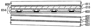
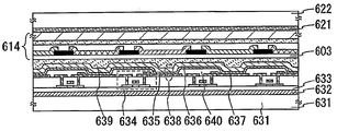
| KR102179165B1 (ko) | 2017-11-28 | 2020-11-16 | 삼성전자주식회사 | 캐리어 기판 및 상기 캐리어 기판을 이용한 반도체 패키지의 제조방법 |
| CN109872642B (zh) * | 2017-12-04 | 2021-05-18 | 利亚德光电股份有限公司 | 小间距led显示模块及其制作方法 |
| CN108735865B (zh) * | 2018-05-26 | 2019-11-01 | 矽照光电(厦门)有限公司 | 一种显示结构生产方法 |
| TWI679627B (zh) * | 2018-06-28 | 2019-12-11 | 友達光電股份有限公司 | 顯示裝置 |
| US10360825B1 (en) * | 2018-09-24 | 2019-07-23 | Innolux Corporation | Flexible electronic device |
| WO2020065856A1 (ja) * | 2018-09-27 | 2020-04-02 | シャープ株式会社 | 表示装置の製造方法 |
| US11668977B2 (en) | 2018-12-14 | 2023-06-06 | 3M Innovative Properties Company | Liquid crystal display having a frontside light control film |
| JP7332147B2 (ja) * | 2019-08-26 | 2023-08-23 | 株式会社Joled | 表示パネル、および、表示パネルの製造方法 |
| CN112442402B (zh) * | 2019-09-05 | 2025-01-24 | 中国石油化工股份有限公司 | 一种酸气的分离工艺 |
| US20220209193A1 (en) * | 2020-12-31 | 2022-06-30 | Samsung Display Co., Ltd. | Display panel, display device including the same, and method for manufacturing the display panel |
| JP2024000195A (ja) * | 2022-06-20 | 2024-01-05 | キオクシア株式会社 | 半導体装置の製造方法 |
Family Cites Families (64)
| Publication number | Priority date | Publication date | Assignee | Title |
|---|---|---|---|---|
| US3624273A (en) * | 1968-11-22 | 1971-11-30 | Alfred J Gale | Flat screen display devices using an array of charged particle sources |
| JPS5331971A (en) | 1976-09-06 | 1978-03-25 | Nippon Telegr & Teleph Corp <Ntt> | Forming method of metal oxide film or semiconductor oxide film |
| US4800100A (en) * | 1987-10-27 | 1989-01-24 | Massachusetts Institute Of Technology | Combined ion and molecular beam apparatus and method for depositing materials |
| US5156720A (en) * | 1989-02-02 | 1992-10-20 | Alcan International Limited | Process for producing released vapor deposited films and product produced thereby |
| JP2617798B2 (ja) * | 1989-09-22 | 1997-06-04 | 三菱電機株式会社 | 積層型半導体装置およびその製造方法 |
| JPH0553008A (ja) * | 1991-08-27 | 1993-03-05 | Kyocera Corp | カラーフイルタ |
| JP2849008B2 (ja) | 1992-11-02 | 1999-01-20 | 三容真空工業株式会社 | カラー液晶表示装置 |
| DE4433330C2 (de) * | 1994-09-19 | 1997-01-30 | Fraunhofer Ges Forschung | Verfahren zur Herstellung von Halbleiterstrukturen mit vorteilhaften Hochfrequenzeigenschaften sowie eine Halbleiterwaferstruktur |
| US5757456A (en) * | 1995-03-10 | 1998-05-26 | Semiconductor Energy Laboratory Co., Ltd. | Display device and method of fabricating involving peeling circuits from one substrate and mounting on other |
| FR2744285B1 (fr) * | 1996-01-25 | 1998-03-06 | Commissariat Energie Atomique | Procede de transfert d'une couche mince d'un substrat initial sur un substrat final |
| EP1655633A3 (en) * | 1996-08-27 | 2006-06-21 | Seiko Epson Corporation | Exfoliating method, transferring method of thin film device, thin film integrated circuit device, and liquid crystal display device |
| SG65697A1 (en) * | 1996-11-15 | 1999-06-22 | Canon Kk | Process for producing semiconductor article |
| US6033995A (en) * | 1997-09-16 | 2000-03-07 | Trw Inc. | Inverted layer epitaxial liftoff process |
| JP3395661B2 (ja) * | 1998-07-07 | 2003-04-14 | 信越半導体株式会社 | Soiウエーハの製造方法 |
| US6274887B1 (en) * | 1998-11-02 | 2001-08-14 | Semiconductor Energy Laboratory Co., Ltd. | Semiconductor device and manufacturing method therefor |
| US6590229B1 (en) * | 1999-01-21 | 2003-07-08 | Semiconductor Energy Laboratory Co., Ltd. | Semiconductor device and process for production thereof |
| US6278841B1 (en) * | 1999-07-26 | 2001-08-21 | Eastman Kodak Company | Camera having label mounted electrical component |
| JP2001075124A (ja) * | 1999-09-02 | 2001-03-23 | Toppan Printing Co Ltd | 液晶表示装置用電極基板の製造方法及び液晶表示装置 |
| TW522453B (en) * | 1999-09-17 | 2003-03-01 | Semiconductor Energy Lab | Display device |
| JP4942867B2 (ja) | 1999-09-17 | 2012-05-30 | 株式会社半導体エネルギー研究所 | El表示装置及び電子装置 |
| JP3942770B2 (ja) * | 1999-09-22 | 2007-07-11 | 株式会社半導体エネルギー研究所 | El表示装置及び電子装置 |
| US6641933B1 (en) * | 1999-09-24 | 2003-11-04 | Semiconductor Energy Laboratory Co., Ltd. | Light-emitting EL display device |
| US6646692B2 (en) * | 2000-01-26 | 2003-11-11 | Semiconductor Energy Laboratory Co., Ltd. | Liquid-crystal display device and method of fabricating the same |
| JP4712198B2 (ja) | 2000-02-01 | 2011-06-29 | 株式会社半導体エネルギー研究所 | 表示装置の作製方法 |
| TW494447B (en) * | 2000-02-01 | 2002-07-11 | Semiconductor Energy Lab | Semiconductor device and manufacturing method thereof |
| JP2001291850A (ja) * | 2000-04-10 | 2001-10-19 | Hitachi Cable Ltd | 結晶シリコン薄膜の製造方法 |
| US7579203B2 (en) * | 2000-04-25 | 2009-08-25 | Semiconductor Energy Laboratory Co., Ltd. | Light emitting device |
| US6562648B1 (en) * | 2000-08-23 | 2003-05-13 | Xerox Corporation | Structure and method for separation and transfer of semiconductor thin films onto dissimilar substrate materials |
| KR20020027930A (ko) | 2000-10-06 | 2002-04-15 | 김순택 | 플라스틱 기판을 이용한 유기 발광 표시장치 |
| FR2817395B1 (fr) * | 2000-11-27 | 2003-10-31 | Soitec Silicon On Insulator | Procede de fabrication d'un substrat notamment pour l'optique, l'electronique ou l'optoelectronique et substrat obtenu par ce procede |
| AUPR216700A0 (en) * | 2000-12-19 | 2001-01-25 | Woodside Energy Limited | Method for separation of non-hydrocarbon gases from hydrocarbon gases |
| TW545080B (en) * | 2000-12-28 | 2003-08-01 | Semiconductor Energy Lab | Light emitting device and method of manufacturing the same |
| JP4059475B2 (ja) * | 2001-03-12 | 2008-03-12 | 日東電工株式会社 | カラーフィルター付き樹脂シートとその製造方法および液晶表示装置 |
| JP4801278B2 (ja) * | 2001-04-23 | 2011-10-26 | 株式会社半導体エネルギー研究所 | 発光装置及びその作製方法 |
| US6808773B2 (en) | 2001-05-24 | 2004-10-26 | Kyodo Printing Co., Ltd. | Shielding base member and method of manufacturing the same |
| JP3923339B2 (ja) | 2002-02-28 | 2007-05-30 | 共同印刷株式会社 | シールド材の製造方法 |
| JP4019305B2 (ja) * | 2001-07-13 | 2007-12-12 | セイコーエプソン株式会社 | 薄膜装置の製造方法 |
| US8415208B2 (en) * | 2001-07-16 | 2013-04-09 | Semiconductor Energy Laboratory Co., Ltd. | Semiconductor device and peeling off method and method of manufacturing semiconductor device |
| JP4567282B2 (ja) | 2001-07-16 | 2010-10-20 | 株式会社半導体エネルギー研究所 | 発光装置の作製方法 |
| JP4027740B2 (ja) * | 2001-07-16 | 2007-12-26 | 株式会社半導体エネルギー研究所 | 半導体装置の作製方法 |
| JP2003109773A (ja) | 2001-07-27 | 2003-04-11 | Semiconductor Energy Lab Co Ltd | 発光装置、半導体装置およびそれらの作製方法 |
| JP5057619B2 (ja) | 2001-08-01 | 2012-10-24 | 株式会社半導体エネルギー研究所 | 半導体装置の作製方法 |
| US7351300B2 (en) * | 2001-08-22 | 2008-04-01 | Semiconductor Energy Laboratory Co., Ltd. | Peeling method and method of manufacturing semiconductor device |
| KR100944886B1 (ko) * | 2001-10-30 | 2010-03-03 | 가부시키가이샤 한도오따이 에네루기 켄큐쇼 | 반도체 장치의 제조 방법 |
| JP3724725B2 (ja) | 2001-11-01 | 2005-12-07 | ソニー株式会社 | 表示装置の製造方法 |
| TWI264121B (en) | 2001-11-30 | 2006-10-11 | Semiconductor Energy Lab | A display device, a method of manufacturing a semiconductor device, and a method of manufacturing a display device |
| JP2003229548A (ja) * | 2001-11-30 | 2003-08-15 | Semiconductor Energy Lab Co Ltd | 乗物、表示装置、および半導体装置の作製方法 |
| US6953735B2 (en) * | 2001-12-28 | 2005-10-11 | Semiconductor Energy Laboratory Co., Ltd. | Method for fabricating a semiconductor device by transferring a layer to a support with curvature |
| JP2003298284A (ja) | 2002-04-02 | 2003-10-17 | Kyodo Printing Co Ltd | シールド材及びその製造方法 |
| JP4410456B2 (ja) * | 2002-04-24 | 2010-02-03 | 株式会社リコー | 薄膜デバイス装置の製造方法、およびアクティブマトリクス基板の製造方法 |
| US7223672B2 (en) * | 2002-04-24 | 2007-05-29 | E Ink Corporation | Processes for forming backplanes for electro-optic displays |
| TWI272641B (en) * | 2002-07-16 | 2007-02-01 | Semiconductor Energy Lab | Method of manufacturing a semiconductor device |
| CN100466285C (zh) * | 2002-09-11 | 2009-03-04 | 株式会社半导体能源研究所 | 发光装置及其制造方法 |
| WO2004040648A1 (ja) * | 2002-10-30 | 2004-05-13 | Semiconductor Energy Laboratory Co., Ltd. | 半導体装置および半導体装置の作製方法 |
| EP1434264A3 (en) * | 2002-12-27 | 2017-01-18 | Semiconductor Energy Laboratory Co., Ltd. | Semiconductor device and manufacturing method using the transfer technique |
| JP2004319538A (ja) * | 2003-04-10 | 2004-11-11 | Seiko Epson Corp | 半導体装置の製造方法、集積回路、電子光学装置及び電子機器 |
| JP2005011794A (ja) * | 2003-05-22 | 2005-01-13 | Tohoku Pioneer Corp | 有機elパネル及びその製造方法 |
| JP3855270B2 (ja) | 2003-05-29 | 2006-12-06 | ソニー株式会社 | アンテナ実装方法 |
| WO2005041249A2 (en) * | 2003-10-28 | 2005-05-06 | Semiconductor Energy Laboratory Co., Ltd. | Method of manufacturing optical film |
| KR101061730B1 (ko) * | 2003-11-28 | 2011-09-05 | 가부시키가이샤 한도오따이 에네루기 켄큐쇼 | 발광 장치 및 그 제조 방법 |
| KR20110091797A (ko) * | 2003-11-28 | 2011-08-12 | 가부시키가이샤 한도오따이 에네루기 켄큐쇼 | 발광 장치 |
| US7084045B2 (en) * | 2003-12-12 | 2006-08-01 | Seminconductor Energy Laboratory Co., Ltd. | Method for manufacturing semiconductor device |
| US7041520B1 (en) * | 2004-10-18 | 2006-05-09 | Softpixel, Inc. | Method for fabricating liquid crystal displays with plastic film substrate |
| US7166520B1 (en) * | 2005-08-08 | 2007-01-23 | Silicon Genesis Corporation | Thin handle substrate method and structure for fabricating devices using one or more films provided by a layer transfer process |
-
2004
- 2004-11-18 KR KR1020117015092A patent/KR20110091797A/ko not_active Ceased
- 2004-11-18 CN CN200480035192A patent/CN100583193C/zh not_active Expired - Fee Related
- 2004-11-18 WO PCT/JP2004/017537 patent/WO2005052893A1/en not_active Ceased
- 2004-11-18 KR KR1020067012918A patent/KR101095293B1/ko not_active Expired - Fee Related
- 2004-11-18 US US10/580,464 patent/US7601236B2/en not_active Expired - Fee Related
- 2004-11-26 JP JP2004341712A patent/JP4578951B2/ja not_active Expired - Fee Related
-
2009
- 2009-10-09 US US12/576,270 patent/US7935969B2/en not_active Expired - Lifetime
-
2011
- 2011-04-28 US US13/096,240 patent/US8581491B2/en not_active Expired - Fee Related
-
2013
- 2013-11-07 US US14/074,063 patent/US9004970B2/en not_active Expired - Lifetime
-
2015
- 2015-03-17 US US14/659,968 patent/US9666752B2/en not_active Expired - Fee Related
-
2017
- 2017-05-25 US US15/605,086 patent/US10128402B2/en not_active Expired - Lifetime
Also Published As
| Publication number | Publication date |
|---|---|
| US20170263806A1 (en) | 2017-09-14 |
| US7601236B2 (en) | 2009-10-13 |
| WO2005052893A1 (en) | 2005-06-09 |
| US9004970B2 (en) | 2015-04-14 |
| US9666752B2 (en) | 2017-05-30 |
| US20110198601A1 (en) | 2011-08-18 |
| US20140060728A1 (en) | 2014-03-06 |
| US10128402B2 (en) | 2018-11-13 |
| US7935969B2 (en) | 2011-05-03 |
| CN1886769A (zh) | 2006-12-27 |
| US20150187984A1 (en) | 2015-07-02 |
| US8581491B2 (en) | 2013-11-12 |
| US20100067235A1 (en) | 2010-03-18 |
| JP2005183374A (ja) | 2005-07-07 |
| CN100583193C (zh) | 2010-01-20 |
| KR101095293B1 (ko) | 2011-12-16 |
| JP4578951B2 (ja) | 2010-11-10 |
| US20070181246A1 (en) | 2007-08-09 |
| KR20060116842A (ko) | 2006-11-15 |
Similar Documents
| Publication | Publication Date | Title |
|---|---|---|
| KR101095293B1 (ko) | 표시 장치 제조 방법 | |
| KR101061730B1 (ko) | 발광 장치 및 그 제조 방법 | |
| US7800113B2 (en) | Method for manufacturing display device | |
| US7084045B2 (en) | Method for manufacturing semiconductor device | |
| US7223641B2 (en) | Semiconductor device, method for manufacturing the same, liquid crystal television and EL television | |
| US7939888B2 (en) | Display device and television device using the same | |
| CN100489569C (zh) | 制作光学膜的方法 | |
| TWI286338B (en) | Semiconductor device and manufacturing method thereof | |
| JP4689249B2 (ja) | 表示装置の作製方法 | |
| JP4836445B2 (ja) | 半導体装置の作製方法 |
Legal Events
| Date | Code | Title | Description |
|---|---|---|---|
| A107 | Divisional application of patent | ||
| PA0104 | Divisional application for international application |
Comment text: Divisional Application for International Patent Patent event code: PA01041R01D Patent event date: 20110630 |
|
| A201 | Request for examination | ||
| PA0201 | Request for examination |
Patent event code: PA02012R01D Patent event date: 20110729 Comment text: Request for Examination of Application |
|
| PG1501 | Laying open of application | ||
| E902 | Notification of reason for refusal | ||
| PE0902 | Notice of grounds for rejection |
Comment text: Notification of reason for refusal Patent event date: 20111011 Patent event code: PE09021S01D |
|
| E90F | Notification of reason for final refusal | ||
| PE0902 | Notice of grounds for rejection |
Comment text: Final Notice of Reason for Refusal Patent event date: 20120511 Patent event code: PE09021S02D |
|
| E601 | Decision to refuse application | ||
| PE0601 | Decision on rejection of patent |
Patent event date: 20121121 Comment text: Decision to Refuse Application Patent event code: PE06012S01D Patent event date: 20120511 Comment text: Final Notice of Reason for Refusal Patent event code: PE06011S02I Patent event date: 20111011 Comment text: Notification of reason for refusal Patent event code: PE06011S01I |
|
| J201 | Request for trial against refusal decision | ||
| PJ0201 | Trial against decision of rejection |
Patent event date: 20121224 Comment text: Request for Trial against Decision on Refusal Patent event code: PJ02012R01D Patent event date: 20121121 Comment text: Decision to Refuse Application Patent event code: PJ02011S01I Appeal kind category: Appeal against decision to decline refusal Appeal identifier: 2012101010759 Request date: 20121224 |
|
| J301 | Trial decision |
Free format text: TRIAL DECISION FOR APPEAL AGAINST DECISION TO DECLINE REFUSAL REQUESTED 20121224 Effective date: 20140422 |
|
| PJ1301 | Trial decision |
Patent event code: PJ13011S01D Patent event date: 20140422 Comment text: Trial Decision on Objection to Decision on Refusal Appeal kind category: Appeal against decision to decline refusal Request date: 20121224 Decision date: 20140422 Appeal identifier: 2012101010759 |