KR20110091797A - A light emitting device - Google Patents
A light emitting device Download PDFInfo
- Publication number
- KR20110091797A KR20110091797A KR1020117015092A KR20117015092A KR20110091797A KR 20110091797 A KR20110091797 A KR 20110091797A KR 1020117015092 A KR1020117015092 A KR 1020117015092A KR 20117015092 A KR20117015092 A KR 20117015092A KR 20110091797 A KR20110091797 A KR 20110091797A
- Authority
- KR
- South Korea
- Prior art keywords
- substrate
- film
- oxide film
- light emitting
- layer
- Prior art date
Links
Images


Classifications
-
- H—ELECTRICITY
- H01—ELECTRIC ELEMENTS
- H01L—SEMICONDUCTOR DEVICES NOT COVERED BY CLASS H10
- H01L33/00—Semiconductor devices with at least one potential-jump barrier or surface barrier specially adapted for light emission; Processes or apparatus specially adapted for the manufacture or treatment thereof or of parts thereof; Details thereof
- H01L33/005—Processes
-
- G—PHYSICS
- G02—OPTICS
- G02F—OPTICAL DEVICES OR ARRANGEMENTS FOR THE CONTROL OF LIGHT BY MODIFICATION OF THE OPTICAL PROPERTIES OF THE MEDIA OF THE ELEMENTS INVOLVED THEREIN; NON-LINEAR OPTICS; FREQUENCY-CHANGING OF LIGHT; OPTICAL LOGIC ELEMENTS; OPTICAL ANALOGUE/DIGITAL CONVERTERS
- G02F1/00—Devices or arrangements for the control of the intensity, colour, phase, polarisation or direction of light arriving from an independent light source, e.g. switching, gating or modulating; Non-linear optics
- G02F1/01—Devices or arrangements for the control of the intensity, colour, phase, polarisation or direction of light arriving from an independent light source, e.g. switching, gating or modulating; Non-linear optics for the control of the intensity, phase, polarisation or colour
- G02F1/13—Devices or arrangements for the control of the intensity, colour, phase, polarisation or direction of light arriving from an independent light source, e.g. switching, gating or modulating; Non-linear optics for the control of the intensity, phase, polarisation or colour based on liquid crystals, e.g. single liquid crystal display cells
- G02F1/133—Constructional arrangements; Operation of liquid crystal cells; Circuit arrangements
- G02F1/1333—Constructional arrangements; Manufacturing methods
- G02F1/133305—Flexible substrates, e.g. plastics, organic film
-
- G—PHYSICS
- G02—OPTICS
- G02F—OPTICAL DEVICES OR ARRANGEMENTS FOR THE CONTROL OF LIGHT BY MODIFICATION OF THE OPTICAL PROPERTIES OF THE MEDIA OF THE ELEMENTS INVOLVED THEREIN; NON-LINEAR OPTICS; FREQUENCY-CHANGING OF LIGHT; OPTICAL LOGIC ELEMENTS; OPTICAL ANALOGUE/DIGITAL CONVERTERS
- G02F1/00—Devices or arrangements for the control of the intensity, colour, phase, polarisation or direction of light arriving from an independent light source, e.g. switching, gating or modulating; Non-linear optics
- G02F1/01—Devices or arrangements for the control of the intensity, colour, phase, polarisation or direction of light arriving from an independent light source, e.g. switching, gating or modulating; Non-linear optics for the control of the intensity, phase, polarisation or colour
- G02F1/13—Devices or arrangements for the control of the intensity, colour, phase, polarisation or direction of light arriving from an independent light source, e.g. switching, gating or modulating; Non-linear optics for the control of the intensity, phase, polarisation or colour based on liquid crystals, e.g. single liquid crystal display cells
- G02F1/133—Constructional arrangements; Operation of liquid crystal cells; Circuit arrangements
- G02F1/1333—Constructional arrangements; Manufacturing methods
-
- H—ELECTRICITY
- H01—ELECTRIC ELEMENTS
- H01L—SEMICONDUCTOR DEVICES NOT COVERED BY CLASS H10
- H01L27/00—Devices consisting of a plurality of semiconductor or other solid-state components formed in or on a common substrate
- H01L27/02—Devices consisting of a plurality of semiconductor or other solid-state components formed in or on a common substrate including semiconductor components specially adapted for rectifying, oscillating, amplifying or switching and having at least one potential-jump barrier or surface barrier; including integrated passive circuit elements with at least one potential-jump barrier or surface barrier
- H01L27/12—Devices consisting of a plurality of semiconductor or other solid-state components formed in or on a common substrate including semiconductor components specially adapted for rectifying, oscillating, amplifying or switching and having at least one potential-jump barrier or surface barrier; including integrated passive circuit elements with at least one potential-jump barrier or surface barrier the substrate being other than a semiconductor body, e.g. an insulating body
- H01L27/1214—Devices consisting of a plurality of semiconductor or other solid-state components formed in or on a common substrate including semiconductor components specially adapted for rectifying, oscillating, amplifying or switching and having at least one potential-jump barrier or surface barrier; including integrated passive circuit elements with at least one potential-jump barrier or surface barrier the substrate being other than a semiconductor body, e.g. an insulating body comprising a plurality of TFTs formed on a non-semiconducting substrate, e.g. driving circuits for AMLCDs
- H01L27/1259—Multistep manufacturing methods
- H01L27/1262—Multistep manufacturing methods with a particular formation, treatment or coating of the substrate
- H01L27/1266—Multistep manufacturing methods with a particular formation, treatment or coating of the substrate the substrate on which the devices are formed not being the final device substrate, e.g. using a temporary substrate
-
- H—ELECTRICITY
- H01—ELECTRIC ELEMENTS
- H01L—SEMICONDUCTOR DEVICES NOT COVERED BY CLASS H10
- H01L27/00—Devices consisting of a plurality of semiconductor or other solid-state components formed in or on a common substrate
- H01L27/15—Devices consisting of a plurality of semiconductor or other solid-state components formed in or on a common substrate including semiconductor components with at least one potential-jump barrier or surface barrier specially adapted for light emission
-
- H—ELECTRICITY
- H10—SEMICONDUCTOR DEVICES; ELECTRIC SOLID-STATE DEVICES NOT OTHERWISE PROVIDED FOR
- H10K—ORGANIC ELECTRIC SOLID-STATE DEVICES
- H10K50/00—Organic light-emitting devices
- H10K50/80—Constructional details
- H10K50/84—Passivation; Containers; Encapsulations
- H10K50/841—Self-supporting sealing arrangements
-
- H—ELECTRICITY
- H10—SEMICONDUCTOR DEVICES; ELECTRIC SOLID-STATE DEVICES NOT OTHERWISE PROVIDED FOR
- H10K—ORGANIC ELECTRIC SOLID-STATE DEVICES
- H10K59/00—Integrated devices, or assemblies of multiple devices, comprising at least one organic light-emitting element covered by group H10K50/00
- H10K59/10—OLED displays
- H10K59/12—Active-matrix OLED [AMOLED] displays
-
- H—ELECTRICITY
- H10—SEMICONDUCTOR DEVICES; ELECTRIC SOLID-STATE DEVICES NOT OTHERWISE PROVIDED FOR
- H10K—ORGANIC ELECTRIC SOLID-STATE DEVICES
- H10K59/00—Integrated devices, or assemblies of multiple devices, comprising at least one organic light-emitting element covered by group H10K50/00
- H10K59/30—Devices specially adapted for multicolour light emission
- H10K59/38—Devices specially adapted for multicolour light emission comprising colour filters or colour changing media [CCM]
-
- H—ELECTRICITY
- H10—SEMICONDUCTOR DEVICES; ELECTRIC SOLID-STATE DEVICES NOT OTHERWISE PROVIDED FOR
- H10K—ORGANIC ELECTRIC SOLID-STATE DEVICES
- H10K71/00—Manufacture or treatment specially adapted for the organic devices covered by this subclass
-
- H—ELECTRICITY
- H10—SEMICONDUCTOR DEVICES; ELECTRIC SOLID-STATE DEVICES NOT OTHERWISE PROVIDED FOR
- H10K—ORGANIC ELECTRIC SOLID-STATE DEVICES
- H10K71/00—Manufacture or treatment specially adapted for the organic devices covered by this subclass
- H10K71/80—Manufacture or treatment specially adapted for the organic devices covered by this subclass using temporary substrates
-
- H—ELECTRICITY
- H10—SEMICONDUCTOR DEVICES; ELECTRIC SOLID-STATE DEVICES NOT OTHERWISE PROVIDED FOR
- H10K—ORGANIC ELECTRIC SOLID-STATE DEVICES
- H10K77/00—Constructional details of devices covered by this subclass and not covered by groups H10K10/80, H10K30/80, H10K50/80 or H10K59/80
- H10K77/10—Substrates, e.g. flexible substrates
-
- H—ELECTRICITY
- H01—ELECTRIC ELEMENTS
- H01L—SEMICONDUCTOR DEVICES NOT COVERED BY CLASS H10
- H01L2933/00—Details relating to devices covered by the group H01L33/00 but not provided for in its subgroups
- H01L2933/0008—Processes
- H01L2933/0025—Processes relating to coatings
-
- H—ELECTRICITY
- H10—SEMICONDUCTOR DEVICES; ELECTRIC SOLID-STATE DEVICES NOT OTHERWISE PROVIDED FOR
- H10K—ORGANIC ELECTRIC SOLID-STATE DEVICES
- H10K59/00—Integrated devices, or assemblies of multiple devices, comprising at least one organic light-emitting element covered by group H10K50/00
- H10K59/10—OLED displays
- H10K59/12—Active-matrix OLED [AMOLED] displays
- H10K59/1201—Manufacture or treatment
-
- Y—GENERAL TAGGING OF NEW TECHNOLOGICAL DEVELOPMENTS; GENERAL TAGGING OF CROSS-SECTIONAL TECHNOLOGIES SPANNING OVER SEVERAL SECTIONS OF THE IPC; TECHNICAL SUBJECTS COVERED BY FORMER USPC CROSS-REFERENCE ART COLLECTIONS [XRACs] AND DIGESTS
- Y02—TECHNOLOGIES OR APPLICATIONS FOR MITIGATION OR ADAPTATION AGAINST CLIMATE CHANGE
- Y02E—REDUCTION OF GREENHOUSE GAS [GHG] EMISSIONS, RELATED TO ENERGY GENERATION, TRANSMISSION OR DISTRIBUTION
- Y02E10/00—Energy generation through renewable energy sources
- Y02E10/50—Photovoltaic [PV] energy
- Y02E10/549—Organic PV cells
-
- Y—GENERAL TAGGING OF NEW TECHNOLOGICAL DEVELOPMENTS; GENERAL TAGGING OF CROSS-SECTIONAL TECHNOLOGIES SPANNING OVER SEVERAL SECTIONS OF THE IPC; TECHNICAL SUBJECTS COVERED BY FORMER USPC CROSS-REFERENCE ART COLLECTIONS [XRACs] AND DIGESTS
- Y02—TECHNOLOGIES OR APPLICATIONS FOR MITIGATION OR ADAPTATION AGAINST CLIMATE CHANGE
- Y02P—CLIMATE CHANGE MITIGATION TECHNOLOGIES IN THE PRODUCTION OR PROCESSING OF GOODS
- Y02P70/00—Climate change mitigation technologies in the production process for final industrial or consumer products
- Y02P70/50—Manufacturing or production processes characterised by the final manufactured product
Abstract
고수율로 우수한 내충격 특성을 구비한 디스플레이를 제조하는 방법을 제공하기 위한 것으로, 플라스틱 기판을 사용하여 형성된 광학 필름을 구비한 표시 장치 제조 방법. 표시 장치 제조 방법은 금속막, 산화막 및 광학 필터를 제1 기판 상에 적층하는 단계; 광학 필터를 제1 기판으로부터 분리하는 단계; 광학 필터를 제2 기판에 부착하는 단계; 화소를 포함하는 층을 제3 기판 상에 형성하는 단계; 및 화소를 포함하는 층을 광학 필터에 부착하는 단계를 포함한다.A display device manufacturing method comprising an optical film formed by using a plastic substrate, to provide a method for manufacturing a display having excellent impact resistance properties at high yield. A display device manufacturing method includes stacking a metal film, an oxide film, and an optical filter on a first substrate; Separating the optical filter from the first substrate; Attaching the optical filter to the second substrate; Forming a layer comprising a pixel on the third substrate; And attaching a layer comprising the pixel to the optical filter.
Description
본 발명은 플라스틱 기판을 형성하여 형성된 광학 필름을 구비한 표시 장치를 제공하는 방법에 관한 것이다.The present invention relates to a method for providing a display device having an optical film formed by forming a plastic substrate.
최근에, 절연된 표면을 구비한 기판 상에 형성되는 반도체 박막(대략 수 nm 내지 수백 nm의 두께를 가진)을 사용하여 박막 트랜지스터(TFT)를 형성하는 기술이 관심을 끌고 있다. 박막 트랜지스터는 IC 및 전자장치와 같은 각종 전자 디바이스들에 널리 적용되었다. 특히, 액정 디스플레이 패널 또는 발광 디스플레이 패널용의 스위칭 소자로서 박막 트랜지스터에 관계된 개발이 다급하게 수행되었다.Recently, a technique of forming a thin film transistor (TFT) using a semiconductor thin film (having a thickness of about several nm to several hundred nm) formed on a substrate having an insulated surface has been of interest. Thin film transistors have been widely applied to various electronic devices such as ICs and electronic devices. In particular, development related to thin film transistors has been urgently carried out as switching elements for liquid crystal display panels or light emitting display panels.
액정 디스플레이 패널에서, 액정 재료는 소자 기판과 이 소자 기판에 대향하여 배열된 대향 전극을 구비한 대향 기판 사이에 개재된다. 소자 기판 상에는 반도체들로서 비정질 실리콘 또는 폴리실리콘을 사용한 TFT들이 매트릭스로 배열되고, 각각의 TFT에 각각이 접속되는 화소 전극들, 소스 배선들 및 게이트 배선들이 각각 형성된다. 컬러 디스플레이를 수행하는 컬러 필터가 소자 기판 또는 대향기판 상에 형성된다. 컬러 이미지들을 표시하기 위해서 편광판들이 소자 기판 및 대향기판 상에 광학 셔터들로서 각각 배열된다.In a liquid crystal display panel, a liquid crystal material is interposed between an element substrate and an opposing substrate having opposing electrodes arranged opposite to the element substrate. On the element substrate, TFTs using amorphous silicon or polysilicon as semiconductors are arranged in a matrix, and pixel electrodes, source wirings, and gate wirings, each connected to each TFT, are formed, respectively. A color filter for performing color display is formed on the element substrate or the counter substrate. Polarizers are arranged as optical shutters on the element substrate and the opposing substrate, respectively, for displaying color images.
액정 디스플레이 패널의 컬러 필터는 R(적색), G(녹색), B(청색)로 구성된 유색층들 및 화소들간의 갭들을 덮기 위한 광차폐 마스크(블랙 매트릭스)를 포함하고, 이에 광을 투과시킴으로써 적색, 녹색 및 청색 광들을 추출한다. 컬러 필터용 광차폐 마스크는 일반적으로 금속막 또는 흑색 안료를 함유한 유기막으로부터 만들어진다. 컬러 필터는 화소들에 대응하는 위치에 배열되고, 그럼으로써 각 화소에 대해 추출될 광의 색들을 변경시킬 수 있다. 화소들에 대응하는 위치는 화소 전극에 일치하는 부분을 나타내는 것에 유의한다.The color filter of the liquid crystal display panel includes colored layers composed of R (red), G (green), and B (blue), and a light shielding mask (black matrix) for covering gaps between pixels, and thereby transmitting light Extract red, green and blue lights. Light shielding masks for color filters are generally made from metal films or organic films containing black pigments. The color filter is arranged at a position corresponding to the pixels, thereby changing the colors of light to be extracted for each pixel. Note that the position corresponding to the pixels represents a portion corresponding to the pixel electrode.
발광 표시 장치에 있어서는 각각 적색, 녹색 및 청색 광들을 방출하는 발광 소자들을 매트릭스로 배열함으로써 유색화하는 방법, 백색광을 방출하는 발광 소자를 사용하여 컬러 필터를 이용함으로써 유색화하는 방법 등이 있다. 백색광을 방출하는 발광 소자를 사용하여 컬러 필터를 이용함으로써 유색화하는 방법은 원리적으로 컬러 필터를 사용하는 액정 표시 장치에 있어서의 유색화 방법과 유사하다(특허문헌 1 참조). 특허문헌1: 일본특허출원공개 2001-217072. BACKGROUND OF THE INVENTION A light emitting display device may be colored by arranging light emitting devices emitting red, green, and blue lights in a matrix, and may be colored by using a color filter using light emitting devices emitting white light. The method of colorizing by using a color filter using the light emitting element which emits white light is similar in principle to the coloration method in the liquid crystal display device using a color filter (refer patent document 1). Patent Document 1: Japanese Patent Application Publication 2001-217072.
종래에, 액정 표시 장치에 사용되는 컬러 필터는 유리 기판 상에 형성되었다. 그러므로, 유리 기판 상에 형성된 컬러 필터 및 컬러 필터를 사용하는 액정 표시 장치가 열악한 내충격 특성들을 갖는다는 문제가 있었다. 또한, 유리 기판의 두께가 액정 표시 장치의 두께를 감소시키게 감소될 때, 기판은 파손될 수 있어 수율이 저하하게 된다.Conventionally, the color filter used for a liquid crystal display device was formed on the glass substrate. Therefore, there has been a problem that the liquid crystal display device using the color filter and the color filter formed on the glass substrate has poor impact resistance properties. In addition, when the thickness of the glass substrate is reduced to reduce the thickness of the liquid crystal display device, the substrate may be broken so that the yield decreases.
또한, 유리 기판은 가요성이 없기 때문에, 만곡된 표면을 갖는 표시 장치 상에 컬러 필터를 형성하기는 곤란하였다.In addition, since the glass substrate is not flexible, it was difficult to form a color filter on a display device having a curved surface.
유색 수지 및 안료 분산 수지가 일반적으로 컬러 필터용 원 재료로서 사용되었다. 그러나, 이들 수지들을 경화시키기 위해서 일정 온도로 가열하는 단계가 필요하다. 그러므로, 열가소성 기판 상에 컬러 필터를 형성하기는 곤란하였다.Colored resins and pigment dispersion resins have generally been used as raw materials for color filters. However, heating to a constant temperature is necessary to cure these resins. Therefore, it was difficult to form a color filter on the thermoplastic substrate.
위에 언급한 문제들에 따라서, 본 발명의 목적은 우수한 내충격 특성을 갖는 표시 장치를 고수율로 제조하는 방법, 즉 플라스틱 기판을 사용하여 형성되는 광학 필름을 구비한 표시 장치를 제조하는 방법을 제공하는 것이다.In accordance with the above-mentioned problems, an object of the present invention is to provide a method for producing a display device having excellent impact resistance properties with high yield, that is, a method for manufacturing a display device having an optical film formed using a plastic substrate. will be.
본 발명의 일 양상에 따라서, 제1 금속막, 제1 산화막 및 광학 필터를 제1 기판 상에 순차로 적층하는 제1 단계, 광학 필터에 제2 기판을 부착하는 제2 단계, 상기 제1 기판을 물리적 광학 필터로부터 분리하는 제3 단계 및 제1 내지 제4 단계들 후에 제3 기판의 표면상에 화소를 포함하는 층을 형성하고 광학 필터를 화소를 포함하는 층의 또 다른 표면에 부착하는 제4 단계를 포함하는 표시 장치 제조 방법이 제공된다.According to an aspect of the present invention, a first step of sequentially stacking a first metal film, a first oxide film and an optical filter on a first substrate, a second step of attaching a second substrate to the optical filter, the first substrate Forming a layer comprising pixels on the surface of the third substrate and attaching the optical filter to another surface of the layer comprising pixels after the third and first to fourth steps of separating the from the physical optical filter. A display device manufacturing method comprising four steps is provided.
본 발명의 또 다른 양상에 따라서, 제1 금속막, 제1 산화막 및 광학 필터를 제1 기판 상에 순차로 적층하는 제1 단계, 상기 제1 기판으로부터 광학 필터를 분리하는 제2 단계, 제2 기판을 광학 필터에 부착하는 제3 단계, 제1 내지 제3 단계들 후에 제3 기판 상에 제2 금속막 및 제2 산화막을 적층하여, 화소를 포함하는 층을 산화막의 표면상에 형성하고, 화소를 포함하는 층을 광학 필터에 부착하는 제4 단계; 및 제2 금속막을 제2 산화막에서 분리하고 제4 기판을 분리된 제2 산화막의 또 다른 표면에 부착하는 제5 단계를 포함하는 표시 장치 제조 방법이 제공된다.According to another aspect of the invention, the first step of sequentially stacking the first metal film, the first oxide film and the optical filter on the first substrate, the second step, separating the optical filter from the first substrate, the second After attaching the substrate to the optical filter, the second metal film and the second oxide film are laminated on the third substrate after the first to third steps, thereby forming a layer including the pixel on the surface of the oxide film, Attaching a layer comprising a pixel to the optical filter; And a fifth step of separating the second metal film from the second oxide film and attaching the fourth substrate to another surface of the separated second oxide film.
제1 및 제2 단계들을 수행한 후에, 제3 단계가 수행될 수 있다. 또한 제1 및 제3 단계들을 수행한 후에, 제2 단계가 수행될 수 있다.After performing the first and second steps, a third step may be performed. In addition, after performing the first and third steps, the second step may be performed.
액정 표시 장치, 발광 표시 장치, DMD(디지털 마이크로미러 디바이스), PDP(플라즈마 디스플레이 패널), FED(전계 방출 디스플레이) 및 전기영동 표시 장치(전자 페이퍼)와 같은 표시 장치들은 표시 장치로서 대표적인 예들로서 열거될 수 있다.Display devices such as liquid crystal displays, light emitting displays, digital micromirror devices (DMDs), plasma display panels (PDPs), field emission displays (FEDs), and electrophoretic displays (electronic papers) are listed as representative examples of display devices. Can be.
액정 표시 장치를 사용하는 경우, 액정 재료는 화소 전극과 광학 필터 사이에 채워진다. 화소 전극이 광학 필터 상에 제공될 수 있다. 화소 전극이 액정 재료의 일측에만 형성될 때, 액정 표시 장치는 IPS 모드 디스플레이를 수행할 수 있는 디바이스이다. 2개의 화소 전극들이 액정 재료를 개재하여 제공될 때, 액정 표시 장치는 TN(트위스트 네마틱) 모드 디스플레이, STN(슈퍼 트위스트 네마틱) 모드 디스플레이 및 VA(수직 정렬) 모드 디스플레이를 수행할 수 있는 디바이스이다.When using a liquid crystal display device, the liquid crystal material is filled between the pixel electrode and the optical filter. A pixel electrode can be provided on the optical filter. When the pixel electrode is formed only on one side of the liquid crystal material, the liquid crystal display device is a device capable of performing IPS mode display. When two pixel electrodes are provided via a liquid crystal material, the liquid crystal display is a device capable of performing TN (twist nematic) mode display, STN (super twisted nematic) mode display, and VA (vertical alignment) mode display. to be.
발광 표시 장치를 사용하는 경우에, 발광 소자는 제1 전극, 제2 전극 및 전극들 사이에 제공되는 발광성 물질을 함유한 층을 포함하고, 제1 전극이 제3 기판 상에 제공되고, 제2 전극이 제3 기판의 대향한 기판(즉, 제2 기판 또는 제4 기판) 상에 제공된다. 이러한 구조를 갖는 발광 소자는 수동 매트릭스 구동 디스플레이를 수행한다. 대안적으로, 발광 소자가 제1 화소 전극, 발광성 물질을 함유한 층 및 제3 기판 상에 제공된 제2 화소 전극을 포함하는 경우에, 이러한 구조를 갖는 발광 소자는 능동 매트릭스 구동 디스플레이를 수행한다.In the case of using the light emitting display device, the light emitting element includes a first electrode, a second electrode and a layer containing a light emitting material provided between the electrodes, the first electrode is provided on the third substrate, and the second An electrode is provided on the opposite substrate (ie, the second substrate or the fourth substrate) of the third substrate. The light emitting element having such a structure performs a passive matrix drive display. Alternatively, in the case where the light emitting element includes a first pixel electrode, a layer containing a luminescent material, and a second pixel electrode provided on the third substrate, the light emitting element having such a structure performs an active matrix drive display.
광학 필터는 컬러 필터, 컬러 변환 필터 또는 홀로그램 컬러 필터이다.The optical filter is a color filter, color conversion filter or hologram color filter.
제2 기판은 플라스틱 기판으로 형성된다. 이 경우, 제2 기판 및 광학 필터를 포함하는 광학 필터는 컬러 필터, 컬러 변환 필터 또는 홀로그램 컬러 필터를 구비한 막이다.The second substrate is formed of a plastic substrate. In this case, the optical filter including the second substrate and the optical filter is a film having a color filter, a color conversion filter or a hologram color filter.
광학 필름은 제2 기판으로서 사용될 수 있다. 광학 필터에 대해서, 편광판, 타원 편광판 또는 위상차판 및 편광판으로 구성된 원 편광판, 반사방지막, 시야각 개선막, 보호막, 휘도 개선막, 프리즘 시트, 등이 채용될 수 있다. 광학 필터 및 제4 기판을 포함하는 광학 필름은 복수의 광학특성들을 나타낸다.The optical film can be used as the second substrate. As the optical filter, a polarizing plate, an elliptical polarizing plate or a circular polarizing plate composed of a retardation plate and a polarizing plate, an antireflection film, a viewing angle improving film, a protective film, a brightness improving film, a prism sheet, and the like can be employed. An optical film comprising an optical filter and a fourth substrate exhibits a plurality of optical properties.
본 발명은 다음의 양상들을 또한 포함한다.The invention also includes the following aspects.
본 발명의 일 양상에 따라서, 제1 금속막, 제1 산화막 및 광학 필터를 제1 기판 상에 순차로 적층하고, 제1 지지체가 상기 광학 필터를 통해 상기 제1 기판과 대향하도록 제1 박리 가능한 접착제를 사용하여 상기 광학 필터의 표면에 상기 제1 지지체를 부착하고, 상기 제1 금속막을 물리적 수단에 의해 상기 제1 산화막으로부터 분리하는, 제1 단계; 제2 기판 상에 화소를 포함하는 층을 형성하는 제2 단계; 및 상기 제1 및 제2 단계들 후에 제1 접착 재료를 사용하여 상기 제2 기판의 화소를 포함하는 층의 표면에 상기 제1 산화막을 부착하고 상기 제1 박리 가능한 접착제 및 상기 제1 지지체를 제거하는 제3 단계를 포함하는, 표시 장치 제조 방법이 제공된다.According to one aspect of the present invention, a first metal film, a first oxide film and an optical filter are sequentially stacked on a first substrate, and a first peelable is provided such that a first supporter faces the first substrate through the optical filter. Attaching the first support to the surface of the optical filter using an adhesive and separating the first metal film from the first oxide film by physical means; A second step of forming a layer including pixels on the second substrate; And attaching the first oxide film to the surface of the layer including the pixel of the second substrate using a first adhesive material after the first and second steps and removing the first peelable adhesive and the first support. A display device manufacturing method is provided, including a third step.
상기 제3 단계 후에 제3 기판은 제2 접착 재료를 사용하여 상기 광학 필터의 표면에 부착될 수 있다.After the third step, the third substrate may be attached to the surface of the optical filter using a second adhesive material.
이 경우, 상기 제1 기판 및 상기 제2 기판은 석영 기판, 세라믹 기판, 실리콘 기판, 금속 기판 및 스테인레스 기판 중 하나이고, 상기 제3 기판은 플라스틱, 편광판 또는 위상차판을 갖는 편광판(타원 편광판 또는 원 편광판), 반사 방지막, 시야각 개선막, 보호막, 휘도 개선막, 프리즘 시트, 등 중 하나이다.In this case, the first substrate and the second substrate is one of a quartz substrate, a ceramic substrate, a silicon substrate, a metal substrate, and a stainless substrate, and the third substrate is a polarizing plate (elliptical polarizing plate or circle) having a plastic, a polarizing plate, or a retardation plate. Polarizing plate), an antireflection film, a viewing angle improving film, a protective film, a brightness improving film, a prism sheet, and the like.
제2 단계 또는 제3 단계에서, 제2 기판의 표면에 플라스틱, 편광판, 위상차판을 갖는 편광판(타원 편광판 또는 원 편광판), 반사 방지막, 시야각 개선막, 보호막, 휘도 개선막, 프리즘 시트, 등이 부착될 수 있다. In the second or third step, a polarizing plate (elliptical polarizing plate or circular polarizing plate) having a plastic, a polarizing plate and a retardation plate on the surface of the second substrate, an antireflection film, a viewing angle improving film, a protective film, a brightness improving film, a prism sheet, and the like Can be attached.
또한, 본 발명의 또 다른 양상에 따라서, 제1 금속막, 제1 산화막 및 광학 필터를 제1 기판 상에 순차로 적층하고, 제2 기판이 상기 광학 필터를 통해 상기 제1 기판과 대향하도록 제1 접착 재료를 사용하여 상기 광학 필터의 표면에 상기 제2 기판을 부착하고, 광학 필터를 형성하도록 상기 제1 금속막을 물리적 수단에 의해 상기 제1 산화막으로부터 분리하는, 제1 단계; 제3 기판 상에 화소를 포함하는 층을 형성하는 제2 단계; 및 상기 제1 및 제2 단계들 후에 제2 접착 재료를 사용하여 상기 제3 기판의 화소를 포함하는 층의 표면에 상기 제1 산화막을 부착하고 상기 제1 박리 가능한 접착제 및 상기 제1 지지체를 제거하는 제3 단계를 포함하는, 표시 장치 제조 방법이 제공된다.Further, according to another aspect of the present invention, the first metal film, the first oxide film and the optical filter are sequentially stacked on the first substrate, and the second substrate is made to face the first substrate through the optical filter. A first step of attaching the second substrate to the surface of the optical filter using an adhesive material, and separating the first metal film from the first oxide film by physical means to form an optical filter; Forming a layer including a pixel on a third substrate; And attaching the first oxide film to the surface of the layer including the pixel of the third substrate using a second adhesive material after the first and second steps and removing the first peelable adhesive and the first support. A display device manufacturing method is provided, including a third step.
또한, 본 발명의 또 다른 양상에 따라서, 제1 금속막, 제1 산화막 및 광학 필터를 제1 기판 상에 순차로 적층하고, 제1 지지체가 상기 광학 필터를 통해 상기 제1 기판과 대향하도록 제1 박리 가능한 접착제를 사용하여 상기 광학 필터의 표면에 상기 제1 지지체를 부착하고, 상기 제1 금속막을 물리적 수단에 의해 상기 제1 산화막으로부터 분리하고, 제1 접착 재료를 사용하여 상기 제1 산화막의 표면에 제2 기판을 부착하고, 광학 필름을 형성하기 위해 상기 제1 지지체 및 상기 제1 박리 가능한 접착제를 제거하는, 제1 단계; 제3 기판 상에 화소를 포함하는 층을 형성하는 제2 단계; 및 상기 제1 및 제2 단계들 후에 제2 접착 재료를 사용하여 상기 제3 기판의 화소를 포함하는 층의 표면에 상기 광학 필터를 부착하는 제3 단계를 포함하는, 표시 장치 제조 방법이 제공된다.Further, according to another aspect of the present invention, the first metal film, the first oxide film and the optical filter are sequentially laminated on the first substrate, and the first support is made to face the first substrate through the optical filter. 1 attach the first support to the surface of the optical filter using a peelable adhesive, separate the first metal film from the first oxide film by physical means, and use a first adhesive material to Attaching a second substrate to the surface and removing the first support and the first peelable adhesive to form an optical film; Forming a layer including a pixel on a third substrate; And a third step of attaching the optical filter to the surface of the layer including the pixel of the third substrate using a second adhesive material after the first and second steps. .
상기 제1 기판 및 상기 제3 기판은 석영 기판, 세라믹 기판, 실리콘 기판, 금속 기판 및 스테인레스 기판 중 하나이고, 상기 제2 기판은 플라스틱, 편광판 또는 위상차판을 갖는 편광판(타원 편광판 또는 원 편광판), 반사 방지막, 시야각 개선막, 보호막, 휘도 개선막, 프리즘 시트, 등 중 하나이다.The first substrate and the third substrate are one of a quartz substrate, a ceramic substrate, a silicon substrate, a metal substrate, and a stainless substrate, and the second substrate has a polarizing plate (elliptical polarizing plate or circular polarizing plate) having a plastic, a polarizing plate, or a retardation plate, Antireflection film, viewing angle improvement film, protective film, brightness improving film, prism sheet, and the like.
상기 제2 단계 또는 제3 단계 후에, 상기 제3 기판의 표면에, 플라스틱 또는 편광판 또는 위상차판을 갖는 편광판(타원 편광판 또는 원 편광판), 반사 방지막, 시야각 개선막, 보호막, 휘도 개선막, 프리즘 시트, 등이 부착될 수 있다.After the second or third step, a polarizing plate (elliptical polarizing plate or circular polarizing plate) having a plastic or a polarizing plate or a retardation plate on the surface of the third substrate, an antireflection film, a viewing angle improving film, a protective film, a brightness improving film, a prism sheet , And the like can be attached.
또한, 본 발명의 또 다른 양상에 따라서, 제1 금속막, 제1 산화막 및 광학 필터를 제1 기판 상에 순차로 적층하고, 제2 지지체가 상기 광학 필터를 통해 상기 제1 기판과 대향하도록 제1 박리 가능한 접착제를 사용하여 상기 광학 필터의 표면에 상기 제1 지지체를 부착하고, 상기 제1 금속막을 물리적 수단에 의해 상기 제1 산화막으로부터 분리하는, 제1 단계; 제2 금속막 및 제2 산화막을 제2 기판 상에 순차로 적층하고 상기 제2 산화막 상에 화소를 포함하는 층을 형성하는 제2 단계; 및 상기 제1 및 제2 단계들 후에 제1 접착 재료를 사용하여 상기 제2 기판의 화소를 포함하는 층의 표면에 상기 제1 산화막을 부착하고, 상기 제2 산화막으로부터 상기 제2 금속막을 물리적 수단에 의해 분리하고, 제2 접착 재료를 사용하여 상기 제2 산화막의 표면에 제3 기판을 부착하고, 상기 제1 박리 가능한 접착제 및 상기 제1 지지체를 제거하는, 제3 단계를 포함하는, 표시 장치 제조 방법이 제공된다.Further, according to another aspect of the present invention, the first metal film, the first oxide film and the optical filter are sequentially stacked on the first substrate, and the second support is made to face the first substrate through the optical filter. A first step of attaching the first support to the surface of the optical filter using a peelable adhesive, and separating the first metal film from the first oxide film by physical means; A second step of sequentially stacking a second metal film and a second oxide film on a second substrate and forming a layer including pixels on the second oxide film; And attaching the first oxide film to the surface of the layer including the pixel of the second substrate using a first adhesive material after the first and second steps, and physically attaching the second metal film from the second oxide film. And a third step of attaching a third substrate to the surface of the second oxide film using a second adhesive material and removing the first peelable adhesive and the first support. A manufacturing method is provided.
상기 제3 단계 후에, 제4 기판이 상기 제3 접착 재료를 사용하여 상기 광학 필터의 표면에 부착될 수 있다.After the third step, a fourth substrate may be attached to the surface of the optical filter using the third adhesive material.
이 경우, 상기 제1 기판 및 상기 제2 기판은 석영 기판, 세라믹 기판, 실리콘 기판, 금속 기판 및 스테인레스 기판 중 하나이고, 상기 제3 기판은 플라스틱, 편광판 또는 위상차판을 갖는 편광판(타원 편광판 또는 원 편광판), 반사 방지막, 시야각 개선막, 보호막, 휘도 개선막, 프리즘 시트, 등 중 하나이다.In this case, the first substrate and the second substrate is one of a quartz substrate, a ceramic substrate, a silicon substrate, a metal substrate, and a stainless substrate, and the third substrate is a polarizing plate (elliptical polarizing plate or circle) having a plastic, a polarizing plate, or a retardation plate. Polarizing plate), an antireflection film, a viewing angle improving film, a protective film, a brightness improving film, a prism sheet, and the like.
또한, 본 발명의 또 다른 양상에 따라서, 제1 금속막, 제1 산화막 및 광학 필터를 제1 기판 상에 순차로 적층하고, 제2 기판이 상기 광학 필터를 통해 상기 제1 기판과 대향하도록 제1 접착 재료를 사용하여 상기 광학 필터의 표면에 상기 제2 기판을 부착하고, 상기 제1 박리 가능한 접착제를 사용하여 상기 제2 기판의 표면에 제1 지지체를 부착하고, 광학 필름을 형성하기 위해 상기 제1 금속막을 물리적 수단에 의해 상기 제1 산화막으로부터 분리하는, 제1 단계; 제2 금속막 및 제2 산화막을 제3 기판 상에 순차로 적층하고, 상기 제2 산화막 상에 화소를 포함하는 층을 형성하는, 제2 단계; 및 상기 제1 및 제2 단계들 후에 제2 접착 재료를 사용하여 상기 제3 기판의 화소를 포함하는 층의 표면에 상기 제1 산화막을 부착하고, 물리적 수단에 의해 상기 제2 금속막을 상기 제2 산화막으로부터 분리하고, 제4 기판을 제3 접착 재료를 사용하여 상기 제2 산화막의 표면에 부착하고, 상기 제1 박리 가능한 접착제 및 상기 제1 지지체를 제거하는, 제3 단계를 포함하는, 표시 장치 제조 방법이 제공된다.Further, according to another aspect of the present invention, the first metal film, the first oxide film and the optical filter are sequentially stacked on the first substrate, and the second substrate is made to face the first substrate through the optical filter. 1 attaching the second substrate to the surface of the optical filter using an adhesive material, attaching the first support to the surface of the second substrate using the first peelable adhesive, and forming the optical film to A first step of separating a first metal film from the first oxide film by physical means; A second step of sequentially stacking a second metal film and a second oxide film on a third substrate, and forming a layer including pixels on the second oxide film; And attaching the first oxide film to the surface of the layer including the pixel of the third substrate using a second adhesive material after the first and second steps, and attaching the second metal film to the second metal film by physical means. And a third step of separating from the oxide film, attaching a fourth substrate to the surface of the second oxide film using a third adhesive material, and removing the first peelable adhesive and the first support. A manufacturing method is provided.
또한, 본 발명의 또 다른 양상에 따라서, 제1 금속막, 제1 산화막 및 광학 필터를 제1 기판 상에 순차로 적층하고, 제1 지지체가 상기 광학 필터를 통해 상기 제1 기판과 대향하도록 제1 박리 가능한 접착제를 사용하여 상기 광학 필터의 표면에 상기 제1 지지체를 부착하고, 상기 제1 금속막을 물리적 수단에 의해 상기 제1 산화막으로부터 분리하는, 제1 단계; 제1 접착 재료를 사용하여 상기 제1 산화막의 표면에 제2 기판을 부착하고, 광학 필름을 형성하기 위해서 상기 제1 지지체 및 상기 제1 박리 가능한 접착제를 제거하는, 제2 단계; 및 제3 기판 상에 제2 금속막 및 제2 산화막을 순차로 적층하고, 상기 제2 산화막 상에 화소를 포함하는 층을 형성하는 제3 단계; 및 상기 제1 내지 제3 단계들 후에 제2 접착 재료를 사용하여 상기 제3 기판의 화소를 포함하는 층의 표면에 상기 광학 필터를 부착하고, 물리적 수단에 의해 상기 제2 금속막을 상기 제2 산화막으로부터 분리하고, 제4 기판을 제3 접착 재료를 사용하여 상기 제2 산화막의 표면에 부착하는, 제4 단계를 포함하는, 표시 장치 제조 방법이 제공된다.Further, according to another aspect of the present invention, the first metal film, the first oxide film and the optical filter are sequentially laminated on the first substrate, and the first support is made to face the first substrate through the optical filter. A first step of attaching the first support to the surface of the optical filter using a peelable adhesive, and separating the first metal film from the first oxide film by physical means; Attaching a second substrate to the surface of the first oxide film using a first adhesive material and removing the first support and the first peelable adhesive to form an optical film; And a third step of sequentially stacking a second metal film and a second oxide film on the third substrate, and forming a layer including a pixel on the second oxide film. And attaching the optical filter to a surface of a layer including a pixel of the third substrate using a second adhesive material after the first to third steps, and attaching the second metal film to the second oxide film by physical means. And a fourth step of separating from the substrate and attaching a fourth substrate to the surface of the second oxide film using a third adhesive material.
제1 금속 산화막은 상기 제1 금속막 및 상기 제1 산화막을 형성함과 동시에 상기 제1 금속막과 상기 제1 산화막 사이에 형성된다. 또한, 제2 금속 산화막은 상기 제2 금속막 및 상기 제2 산화막을 형성함과 동시에 상기 제2 금속막과 상기 제2 산화막 사이에 형성된다.The first metal oxide film is formed between the first metal film and the first oxide film while forming the first metal film and the first oxide film. The second metal oxide film is formed between the second metal film and the second oxide film while forming the second metal film and the second oxide film.
상기 제1 산화막은 상기 제1 금속 산화막을 형성하기 위해 상기 제1 금속막의 표면을 산화한 후에 형성된다. 마찬가지로, 상기 제2 산화막은 상기 제2 금속 산화막을 형성하기 위해 상기 제2 금속막의 표면을 산화한 후에 형성된다. The first oxide film is formed after oxidizing the surface of the first metal film to form the first metal oxide film. Similarly, the second oxide film is formed after oxidizing the surface of the second metal film to form the second metal oxide film.
또한, 반도체 소자는 화소 전극에 전기적으로 접속된다. 반도체 소자에 대해서, TFT, 유기 반도체 트랜지스터, 다이오드, MIM 소자, 등이 사용된다.In addition, the semiconductor element is electrically connected to the pixel electrode. As the semiconductor element, a TFT, an organic semiconductor transistor, a diode, a MIM element, or the like is used.
바람직하게, 제1 기판은 내열성 기판이다. 통상적으로, 유리 기판, 석영 기판, 세라믹 기판, 실리콘 기판, 금속 기판 및 스테인레스 기판이 제1 기판으로서 사용될 수 있다.Preferably, the first substrate is a heat resistant substrate. Typically, a glass substrate, a quartz substrate, a ceramic substrate, a silicon substrate, a metal substrate, and a stainless substrate can be used as the first substrate.
제1 및 제2 금속막들은 티탄(Ti), 알루미늄(Al), 탄탈(Ta), 텅스텐(W), 몰리브덴(Mo), 구리(Cu), 크롬(Cr), 네오디뮴(Nd), 철(Fe), 니켈(Ni), 코발트(Co), 루테늄(Ru), 로듐(Rh), 팔라듐(Pd), 오스뮴(Os), 이리듐(Ir)에서 선택되는 원소; 합금 재료 또는 위에 언급된 원소들을 주 성분으로서 함유하는 화합 재료를 포함하는 단일층; 또는 이들의 적층으로 형성될 수 있다.The first and second metal layers include titanium (Ti), aluminum (Al), tantalum (Ta), tungsten (W), molybdenum (Mo), copper (Cu), chromium (Cr), neodymium (Nd), and iron ( Elements selected from Fe), nickel (Ni), cobalt (Co), ruthenium (Ru), rhodium (Rh), palladium (Pd), osmium (Os), and iridium (Ir); A single layer comprising an alloy material or a compound material containing the above-mentioned elements as main components; Or a laminate thereof.
또한, 화소를 포함하는 층의 표면상에 스페이서를 형성한 후에, 이 층은 상기 제2 기판 또는 상기 제3 기판에 부착될 수 있다.Further, after forming a spacer on the surface of the layer including the pixel, the layer can be attached to the second substrate or the third substrate.
본 발명에 따라서, 표시 장치는 디스플레이 소자, 즉 이미지 표시 장치를 사용한 디바이스를 나타낸다. 또한, 표시 장치는 액정소자가 커넥터, 예를 들면, 가요성 인쇄회로(FPC), TAB(테이프 자동 본딩) 테이프 또는 TCP(테이프 캐리어 패키지)로 부착되는 모듈; TAB 테이프 또는 TCP의 단부 상에 제공된 인쇄배선보드를 구비한 모듈; 및 디스플레이 소자가 IC(집적회로) 또는 COG(칩 온 글래스) 기술에 의해 CPU가 직접 장착된 모듈 전부를 포함한다.According to the invention, the display device represents a display element, ie a device using an image display device. In addition, the display device includes a module to which a liquid crystal element is attached by a connector, for example, a flexible printed circuit (FPC), TAB (tape automatic bonding) tape or TCP (tape carrier package); A module having a printed wiring board provided on an end of the TAB tape or TCP; And the display element includes all modules in which the CPU is directly mounted by IC (Integrated Circuit) or COG (Chip on Glass) technology.
본 발명에 따라서, 플라스틱 기판을 포함하는 광학 필름을 갖는 표시 장치가 형성될 수 있다. 결국, 우수한 내충격 특성을 갖는 경량박형 표시 장치가 형성될 수 있다. 또한, 만곡된 표현을 갖는 표시 장치 또는 형태를 가변시킬 수 있는 표시 장치가 제조될 수 있다.According to the present invention, a display device having an optical film including a plastic substrate can be formed. As a result, a lightweight thin display device having excellent impact resistance characteristics can be formed. In addition, a display device having a curved expression or a display device capable of varying the shape can be manufactured.
본 발명에 따른 광학 필름을 사용하는 표시 장치에서, 화소를 포함하는 층 및 광학 필름은 개별적으로 서로 다른 단계들을 통해 형성되고, 이들은 완성 후에 서로 부착된다. 이러한 구조를 사용함으로써, 디스플레이 소자 또는 반도체 소자의 수율 및 광학 필름의 수율이 개별적으로 제어될 수 있고, 그럼으로써 전체 표시 장치의 수율 감소를 억제시킬 수 있다.In the display device using the optical film according to the present invention, the layer including the pixel and the optical film are individually formed through different steps, and they are attached to each other after completion. By using such a structure, the yield of the display element or the semiconductor element and the yield of the optical film can be individually controlled, thereby suppressing the yield reduction of the entire display device.
또한, 능동 매트릭스 기판을 제조하는 단계들 및 광학 필름을 제조하는 단계들은 동시에 진행될 수 있어 표시 장치의 제조 리드 타임을 감소시킨다.In addition, the steps of manufacturing the active matrix substrate and the steps of manufacturing the optical film can be performed simultaneously to reduce the manufacturing lead time of the display device.
도 1a 내지 도 1e는 본 발명에 따른 표시 장치를 제조하는 단계들을 설명하는 단면도.
도 2a 내지 도 2f는 본 발명에 따른 표시 장치를 제조하는 단계들을 설명하는 단면도.
도 3a 내지 도 3f는 본 발명에 따른 표시 장치를 제조하는 단계들을 설명하는 단면도.
도 4a 내지 도 4e는 본 발명에 따른 표시 장치를 제조하는 단계들을 설명하는 단면도.
도 5a 내지 도 5d는 본 발명에 따른 표시 장치를 제조하는 단계들을 설명하는 단면도.
도 6a 및 도 6b는 본 발명에 따른 표시 장치를 제조하는 단계들을 설명하는 단면도.
도 7a 및 도 7b는 본 발명에 따른 표시 장치를 제조하는 단계들을 설명하는 단면도.
도 8a 및 도 8b는 본 발명에 따른 표시 장치를 제조하는 단계들을 설명하는 단면도.
도 9a 내지 도 9c는 본 발명에 따른 표시 장치를 제조하는 단계들을 설명하는 단면도.
도 10a 및 도 10b는 본 발명에 따른 표시 장치를 제조하는 단계들을 설명하는 단면도.
도 11a 및 도 11b는 본 발명에 따른 표시 장치를 제조하는 단계들을 설명하는 단면도.
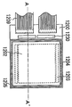
도 12a는 평면도이고 도 12b는 본 발명에 따라 제조된 디스플레이 패널을 도시한 단면도.
도 13a는 평면도이고 도 13b는 본 발명에 따라 제조된 디스플레이 패널을 도시한 단면도.
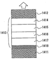
도 14a 및 도 14b는 발광 소자의 구조들을 도시한 도면들.
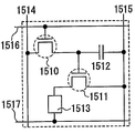
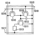
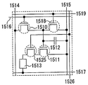
도 15a 내지 도 15c는 발광 소자들을 위한 화소들의 회로도.
도 16a는 평면도이고 도 16b는 본 발명에 따라 제조된 디스플레이 패널을 도시한 단면도.
도 17a는 평면도이고 도 17b는 본 발명에 따라 제조된 디스플레이 패널을 도시한 단면도.
도 18은 전자기기의 구조를 설명하는 도면.
도 19는 전자기기의 구조를 설명하는 도면.
도 20a 및 도 20b는 전자기기의 구조를 설명하는 도면.1A to 1E are cross-sectional views illustrating steps of manufacturing a display device according to the present invention.
2A to 2F are cross-sectional views illustrating steps of manufacturing a display device according to the present invention.
3A to 3F are cross-sectional views illustrating steps of manufacturing a display device according to the present invention.
4A to 4E are cross-sectional views illustrating steps of manufacturing a display device according to the present invention.
5A to 5D are cross-sectional views illustrating steps in manufacturing a display device according to the present invention.
6A and 6B are cross-sectional views illustrating steps of manufacturing a display device according to the present invention.
7A and 7B are cross-sectional views illustrating steps of manufacturing a display device according to the present invention.
8A and 8B are cross-sectional views illustrating steps of manufacturing a display device according to the present invention.
9A to 9C are cross-sectional views illustrating steps in manufacturing a display device according to the present invention.
10A and 10B are cross-sectional views illustrating steps in manufacturing a display device according to the present invention.
11A and 11B are cross-sectional views illustrating steps in manufacturing a display device according to the present invention.
12A is a plan view and FIG. 12B is a sectional view showing a display panel manufactured according to the present invention.
13A is a plan view and FIG. 13B is a sectional view showing a display panel manufactured according to the present invention.
14A and 14B show structures of the light emitting element.
15A-15C are circuit diagrams of pixels for light emitting elements.
16A is a plan view and FIG. 16B is a sectional view showing a display panel manufactured according to the present invention.
17A is a plan view and FIG. 17B is a sectional view showing a display panel manufactured according to the present invention.
18 is a diagram illustrating a structure of an electronic device.
19 illustrates a structure of an electronic device.
20A and 20B illustrate the structure of an electronic device.
실시형태 1Embodiment 1
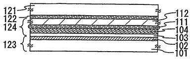
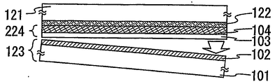
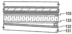
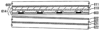
플라스틱 기판을 사용하여 형성되는 광학 필름을 구비한 표시 장치를 제조하는 방법을 도 1a 내지 도 1e를 참조하여 본 실시형태에서 설명한다.The method of manufacturing the display device provided with the optical film formed using a plastic substrate is demonstrated in this embodiment with reference to FIGS. 1A-1E.
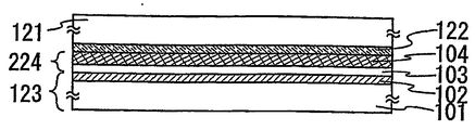
도 1a에 도시한 바와 같이, 제1 금속막(102)이 제1 기판(101) 상에 형성된다. 제1 기판으로서, 내열성 재료, 즉 광학 필터를 제조하고 통상적으로 유리 기판, 석영 기판, 세라믹 기판, 실리콘 기판, 금속 기판 또는 스테인리스 기판을 분리하는 후속의 단계들에서의 열처리에 견딜 수 있는 재료가 사용될 수 있다.As shown in FIG. 1A, a
제1 금속막(102)은 티탄(Ti), 알루미늄(Al), 탄탈(Ta), 텅스텐(W), 몰리브덴(Mo), 구리(Cu), 크롬(Cr), 네오디뮴(Nd), 철(Fe), 니켈(Ni), 코발트(Co), 루테늄(Ru), 로듐(Rh), 팔라듐(Pd), 오스뮴(Os), 이리듐(Ir)에서 선택된 원소; 합금 재료 또는 주성분으로서 위에 언급한 원소들을 함유하는 화합 재료로 형성된 단일 층; 또는 이들의 적층으로 형성될 수 있다. 제1 금속막은 위에 언급된 원소들의 질화물들 또는 이들의 적층으로 형성될 수도 있다. 후속 분리단계의 조건들은 제1 금속막용 합금에 금속의 조성비 또는 함유된 산소 또는 질소의 조성비를 적합하게 조정함으로써 가변되는 것에 유의한다. 그러므로, 분리단계는 다양한 종류의 처리에 맞출 수 있다. 제1 금속막(102)은 10 내지 200nm의 두께, 바람직하게는 50 내지 75nm의 두께를 갖도록 스퍼터링, CVD 및 기상증착과 같은 공지의 제조 방법에 의해 형성된다.The
다음에 제1 금속막(102) 상에 제1 산화막(103)이 형성된다. 이 경우, 제1 금속막(102)과 제1 산화막(103) 사이에 제1 금속 산화막이 형성된다. 후속 단계에서 분리단계를 수행할 때, 분리가 제1 금속 산화막과 제1 산화막간의 계면에서 또는 제1 금속 산화막과 제1 금속막간의 계면에서, 제1 금속 산화막 내에서 야기될 것이다. 제1 산화막(103)에 대해서, 층이 스퍼터링 또는 플라즈마 CVD에 의해 산화 실리콘, 산화 질화 실리콘 또는 금속 산화물로 형성될 수 있다. 제1 산화막(103)의 두께는 제1 금속막(102)보다는 바람직하게는 적어도 2배 또는 더 바람직하게는 제1 금속막(102)보다 적어도 4배 두꺼운 것이 바람직하다. 제1 산화막(103)의 두께는 여기서는 200 내지 800nm, 바람직하게는 200 내지 300nm로 설정된다.Next, a
다음에 제1 산화막(104) 상에 광학 필터(104)가 형성된다. 광학 필터의 대표적인 예로서, 컬러 필터, 컬러 변환 필터, 홀로그램 컬러 필터 등을 열거할 수 있다.Next, the
이어서, 제2 기판(112)이 제1 접착 재료(111)를 사용하여 광학 필터(104)의 표면에 부착된다. 반응성 경화 접착 재료, 열 경화 접착 재료, 자외 경화 접착 재료와 같은 광 경화 접착 재료 및 혐기성 경화 접착 재료를 포함한 여러 종류의 경화 접착 재료들이 접착 재료로서 사용될 수 있다. 이들 재료들의 대표적인 예들로서, 에폭시 수지, 아크릴 수지, 실리콘 수지와 같은 유기 수지를 들 수 있다.Subsequently, the
플라스틱 기판(고분자 재료 또는 수지)가 제2 기판(112)으로서 사용된다. 플라스틱 기판의 대표적인 예들로서, 폴리카보네이트(PC); JSR 사에서 제조한 폴라 라디칼을 가진 노르보넨 수지로 형성된 ARTON; 폴리에칠렌 테레프탈레이트(PET); 폴리에테르 술폰(PES); 폴리에칠렌 나프탈레이트(PEN); 나일론; 폴리에테르 에테르 케톤(PEEK); 폴리술폰(PSF); 폴리에테르이미드(PEI); 폴리아크릴레이트(PAR); 폴리부틸렌(PBT); 및 폴리이미드와 같은 플라스틱 기판들이 사용될 수 있다. 이 외에도, 편광판, 위상차판을 갖는 편광판(타원 편광판 또는 원 편광판), 반사 방지막, 시야각 개선막, 보호막, 휘도 개선막 및 프리즘 시트가 제2 기판으로서 사용될 수 있다.A plastic substrate (polymeric material or resin) is used as the
이어서, 제1 지지체(121)이 제1 박리 가능한 접착제(122)로 제2 기판(112)의 표면에 부착된다. 이 때, 기포가 제2 기판(122) 제1 박리 가능한 접착제(122) 사이에 침입할 때, 광학 필터가 후속 분리단계에서 쉽게 파손될 것이다. 파손을 방지하기 위해서, 이에 제1 지지체가 그들간에 기포가 생기지 않게 부착된다. 테이프 실장기 디바이스 등을 사용하여, 제1 지지체는 기포가 혼합됨이 없이 짧은 시간에 부착될 수 있다.Subsequently, the
바람직하게, 제1 기판(101) 및 제2 기판(112)보다 큰 강성을 갖는 기판, 통상적으로 석영 기판, 금속 기판 또는 세라믹 기판이 제1지지체(121)로서 사용된다.Preferably, a substrate having a greater rigidity than the
제1 박리 가능한 접착제(122)에 대해서, 유기수지로 만들어진 접착 재료가 사용될 수 있다. 대표적으로, 반응성 박리 가능한 접착 재료, 열 박리 가능한 접착 재료, 자외 박리 가능한 접착 재료와 같은 광 박리 가능한 접착 재료 및 혐기성 박리 가능한 접착 재료를 포함하는 다양한 종류의 박리 가능한 접착 재료; 및 전술한 박리 가능한 접착 재료로부터 만들어진 접착 재료들을 양면에 구비한 부재(통상적으로, 양면 테이프 및 양면 시트)를 예로 들 수 있다.For the first
도 1a에서, 제1 기판(101) 및 이 위에 형성된 제1 금속막(102)을 제1 분리체(123)라 칭한다. 또한, 제1 산화막(103) 내지 제2 기판(112)의 층들(즉, 제1 금속막(102)과 제1 박리 가능한 접착제(122)간에 개재된 층들)을 제1 본체(124)라 칭한다.In FIG. 1A, the
각 기판의 파손을 방지하기 위해서 박리 가능한 접착제를 사용하여 제1 기판(101)에 지지체가 접착되는 것이 바람직하다. 지지체를 접착시킴으로써, 후에 수행될 분리단계가 보다 적은 힘으로서 쉽게 수행될 수 있다. 바람직하게, 제1 기판보다 큰 강성을 갖는 기판, 통상적으로 석영 기판, 금속 기판 및 세라믹 기판이 지지체로서 사용된다.In order to prevent breakage of each substrate, it is preferable that the support is adhered to the
도 1b에 도시한 바와 같이, 다음에 제1 분리체(123)가 물리적 수단에 의해 제1 본체(124)로부터 분리된다. 물리적 힘은 예를 들면 핸드 파워, 노즐을 통해 인가된 가스압, 초음파 및 쐐기형 부재를 사용한 로드와 같은 비교적 작은 힘을 말한다.As shown in FIG. 1B, the
결국, 분리는 제1 금속막(102) 내부, 제1 금속 산화막 내지, 제1 금속 산화막과 제1 산화막간 계면에서 또는 제1 금속 산화막과 제1 금속막간의 계면에서 야기되어 제1 분리체(123)가 비교적 작은 힘에 의해 제1 본체(124)로부터 분리될 수 있다.As a result, separation occurs at the interface between the first metal oxide film, the first metal oxide film, and the first metal oxide film and the first oxide film, or at the interface between the first metal oxide film and the first metal film. 123 may be separated from
분리체를 쉽게 분리하기 위해서, 분리단계에 앞선 전 단계로서 전처리가 수행되는 것이 바람직하다. 통상적으로, 제1 금속막(102)과 제1 산화막(103)간에 점착성을 부분적으로 감소시키기 위한 처리가 수행된다. 이들 사이에 점착성을 부분적으로 감소시키는 처리는 분리될 영역의 테두리를 따라 제1 금속막(102)에 레이저빔을 부분적으로 조사하여 수행되거나, 분리할 영역의 테두리를 따라 외부로부터 압력을 국부적으로 가하여 제1 금속막(102) 내부 또는 이의 계면에 부분적으로 손상을 가함으로써 수행된다. 구체적으로, 다이아몬드 펜과 같은 하드 니들을 이에 부하를 가하면서 수직하게 눌러 이동시킬 수도 있다. 0.1 내지 2mm의 가압력을 갖는 압력을 가하면서 하드 니들을 이동시키기 위해 스크라이버 디바이스가 사용되는 것이 바람직하다. 따라서, 분리 현상이 쉽게 야기되는 부분, 즉 분리단계를 수행하기에 앞서 분리현상의 트리거를 형성하는 것이 중요하다. 점착성을 미리 선택적으로(부분적으로) 감소시키는 전처리를 수행함으로써, 빈약한 분리가 방지될 수 있고, 그럼으로써 수율이 향상된다.In order to easily separate the separator, it is preferable that the pretreatment is performed as a previous step prior to the separation step. Usually, a process for partially reducing the adhesiveness between the
전술한 단계들에 따라서, 플라스틱 기판 상에 제공된 광학 필름이 형성될 수 있다. 플라스틱 기판 및 이 위에 형성된 광학 필터(즉, 제1 본체(124)를 여기서는 광학 필름이라 칭한다.According to the above-described steps, an optical film provided on the plastic substrate can be formed. The plastic substrate and the optical filter (ie, the first body 124) formed thereon are referred to herein as optical films.
본 실시형태에 따른 광학 필름에서, 접착 재료(111)인 유기수지는 광학 필터와 제2 기판(112) 사이에 개재되고, 제1 산화막(103)은 유기수지에 접촉하는 표면에 대향하여 있는 광학 필터의 표면상에 제공된다.In the optical film according to the present embodiment, the organic resin, which is the
제2 기판(112)은 평관판, 위상차판, 광 확산막과 같은 광학 필름으로부터 만들어질 수 있다. 제2 기판 또는 산화막의 표면에 공지의 반사 방지막이 제공될 수 있다. 구조를 이용하여, 복수의 광학특성들을 갖는 광학 필름이 형성될 수 있다.The
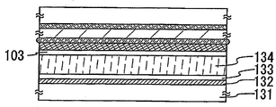
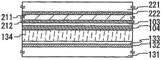
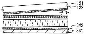
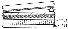
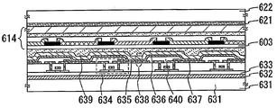
도 1c에 도시한 바와 같이, 제2 금속막(132) 및 제2 산화막(133)이 제3 기판(131) 상에 순차로 형성된다. 제1 기판과 동일한 재료로 형성된 기판이 제3 기판으로서 사용될 수 있다. 또한, 제2 금속막(132)은 제1 금속막(120)과 동일한 제조단계들 및 구조를 사용하여 형성될 수 있다. 마찬가지로, 제1 산화막(103)과 동일한 제조단계들, 재료 및 구조를 사용하여 제2 산화막(133)이 형성될 수 있다.As shown in FIG. 1C, the
화소를 포함하는 층(134)이 제2 산화막(133) 상에 형성된다. 화소를 포함하는 층은 화소로서 기능하는 소자 또는 전극, 전형적으로, 액정소자, 발광 소자, 화소 전극, 마이크로미러 어레이, 전자 에미터 등이 표시 장치에 제공되는 층을 나타낸다. 외에도, 화소를 구동하기 위한 소자, 전형적으로, TFT, 유기 반도체 트랜지스터, 다이오드, MIM 소자, 등이 또한 그 위에 제공될 수 있다.A
제1 본체(124), 즉 도 1b에서 형성된 광학 필름이 화소를 포함하는 층(134)의 표면에 부착된다. 구체적으로, 화소를 포함하는 층(134)의 표면에 제1 본체(124)의 제1 산화막(103)이 제2 접착 재료(도시생략)를 사용하여 부착된다. 제1 접착 재료(111)와 동일한 재료가 제2 접착 재료용으로 사용될 수 있다.The
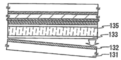
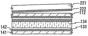
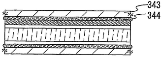
도 1d에 도시한 바와 같이, 도 1b에 도시한 바와 같은 단계와 동일한 방식으로 물리적 수단을 사용하여 제2 산화막(133)이 제2 금속막(132)으로부터 분리된다. 단계에 따라서, 제3 기판(131) 및 제2 금속막(132)이 제2 산화막(133)으로부터 분리된다.As shown in FIG. 1D, the
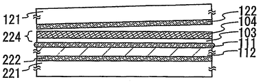
도 1e에 도시한 바와 같이, 제4 기판(141)이 제3 접착 재료(142)로 제2 산화막(133) 또는 제2 금속 산화막의 표면에 부착된다. 제2 기판(122) 뿐만 아니라 제4 기판(141)용으로 플라스틱 기판이 채용될 수 있다. 제1 박리 가능한 접착제(122) 및 제1 지지체(121)이 제2 기판(112)으로부터 분리된다.As shown in FIG. 1E, the
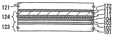
위에 언급된 단계들에 따라서, 플라스틱 기판으로 형성된 광학 필름을 포함하는 표시 장치가 제조될 수 있다. 결국, 우수한 내충격 특성을 갖는 경량, 박형 표시 장치가 형성될 수 있다. 또한, 만곡된 표면을 갖는 표시 장치 또는 형태가 변화될 수 있는 표시 장치가 제조될 수 있다.
According to the above-mentioned steps, a display device including an optical film formed of a plastic substrate can be manufactured. As a result, a lightweight and thin display device having excellent impact resistance characteristics can be formed. In addition, a display device having a curved surface or a display device whose shape can be changed can be manufactured.
실시형태 2Embodiment 2
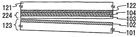
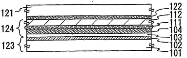
본 실시형태에서, 광학 필름을 제조하는 방법 및 이를 사용하여 표시 장치를 제조하는 방법을 도 2a 내지 도 2f를 참조하여 기술한다. 실시형태의 광학 필름은 광학 필터 및 제2 기판에 대한 접착표면들에 관하여 실시형태 1과는 다른 구조를 포함함에 유의한다.In this embodiment, a method of manufacturing an optical film and a method of manufacturing a display device using the same are described with reference to FIGS. 2A to 2F. Note that the optical film of the embodiment includes a structure different from that of the first embodiment with respect to the adhesive surfaces to the optical filter and the second substrate.
도 2a에 도시한 바와 같이, 제1 금속막(102) 및 제1 산화막(103)이 순차로 제1 기판(101) 상에 형성되고, 광학 필터(104)가 실시형태 1과 동일한 방식으로 제1 산화막(103) 상에 형성된다. 제1 금속 산화막이 제1 금속막과 제1 산화막 사이에 형성됨에 유의한다.As shown in FIG. 2A, the
제1 지지체(121)가 제1 박리 가능한 접착제(122)로 광학 필터(104)의 표면에 부착된다. 제1 기판(101) 및 이 위에 형성된 제1 금속막(102)을 여기서는 제1 분리체(123)라 칭한다. 한편, 제1 산화막(103) 및 광학 필터(104)(즉, 제1 금속막(102)과 제1 박리 가능한 접착제(122) 사이에 개재된 층들)을 본체(224)라 칭한다.The
각 기판의 파손을 방지하기 위해서 박리 가능한 접착제로 제1 기판(101)에 지지체가 접착되는 것이 바람직하다. 그에 지지체를 접착시킴으로써, 후에 수행될 분리단계가 적은 힘으로 쉽게 수행될 수 있다. 바람직하게, 제1 기판보다 큰 강성을 갖는 기판, 전형적으로 석영 기판, 금속 기판 및 세라믹 기판이 지지체로서 사용된다.In order to prevent breakage of each substrate, the support is preferably bonded to the
광학 필터(104)의 표면이 평탄하지 않은 경우에는 광학 필터의 표면에 평탄화 층이 제공될 수 있다. 평탄화층을 제공함으로써, 광학 필터(104)와 제1 박리 가능한 접착제(122) 사이에 기포들이 침입하는 것이 방지될 수 있고, 그럼으로써 분리단계의 신뢰도가 향상된다. 평탄화층은 도포된 절연막 및 유기수지와 같이 도포에 의해 형성될 수 있는 재료로부터 만들어 질 수 있다. 평탄화층이 박리 가능한 재료, 전형적으로 접착 재료를 사용하여 형성될 때, 층이 나중에 제거될 수 있다.If the surface of the
도 2b에 도시한 바와 같이, 제1 분리체(123)가 물리적 수단을 사용하여 제1 본체(224)로부터 분리된다. 분리체를 쉽게 분리하기 위해서, 분리단계 전의 전 단계로서 실시형태1에 기술한 바와 같은 전처리가 수행되는 것이 바람직하다. 전처리를 수행함으로써, 제1 금속 산화막 내에, 제1 금속 산화막과 제1 산화막간 계면에서 또는 제1 금속 산화막과 제1 금속막간의 계면에서 분리가 야기되어 제1 분리체(123)가 비교적 적은 힘으로 제1 본체(224)로부터 분리될 수 있다. 실시형태 1에 설명한 바와 같은 물리적 수단이 적합하게 채용될 수도 있다.As shown in FIG. 2B, the
도 2c에 도시한 바와 같이, 제1 산화막(103) 및 제2 기판(112)이 제1 접착 재료(111)를 사용하여 서로 부착된다. 다음에 제2 지지체(221)가 제2 박리 가능한 접착제(222)를 사용하여 제2 기판의 표면에 부착된다. 후에, 제1 박리 가능한 접착제(122) 및 제1 지지체(121)가 광학 필터(103)로부터 제거된다. 제1 박리 가능한 접착제(122) 및 제1 지지체(121)와 동일한 재료들 및 구조들이 제2 박리 가능한 접착제(222) 및 제2 지지체(221)용으로 각각 사용될 수 있다.As shown in FIG. 2C, the
위에 기술된 단계들에 따라서, 광학 필름이 형성될 수 있다. 즉, 광학 필터(104)가 제2 기판(112) 상에 제공될 수 있다.According to the steps described above, an optical film can be formed. That is, the
실시예에서, 접착 재료(111)인 유기수지와 제1 산화막(103)이 제2 기판(112)과 광학 필터(104) 사이에 개재된다.In an embodiment, the organic resin, which is the
대안적으로, 광학 필터(104)의 표면상에 화소 전극으로서 도전막을 형성한 후에 도 2a 및 도 2b에 도시한 분리단계가 수행될 수도 있다. 단계에 따라서, 화소 전극을 갖는 광학 필름이 형성될 수 있다.Alternatively, after forming the conductive film as the pixel electrode on the surface of the
제2 기판(112)으로서, 평광판; 위상차판을 구비한 평관판(타원 편광판 및 원 편광판; 반사방지막; 시야각 개선막; 보호막; 휘도 개선막; 프리즘 시트 등을 사용하는 것이 가능하다. 또한, 공지의 반사 방지막이 제2 기판의 표면상에 형성될 수 있다. 구조를 이용함으로써, 복수의 광학특성들을 갖는 광학 필름이 형성될 수 있다.A
다음에, 도 2d에 도시한 바와 같이, 실시형태 1과 동일한 방식으로 제3 기판(131) 상에 제2 금속막(132) 및 제2 산화막(133)이 순차로 적층된다.Next, as shown in FIG. 2D, the
화소를 포함하는 층(134)이 제2 산화막(133) 상에 형성된다.A
이어서, 도 2c에서 제조된 광학 필름, 즉 제2 기판 상에 제공된 광학 필터가, 화소를 포함하는 층(134)의 표면에 부착된다. 광학 필름의 광학 필터(104)가, 제2 접착 재료(도시생략)로 화소를 포함하는 층(134)의 표면에 부착된다. 제1 접착 재료와 동일한 재료가 제2 접착 재료용으로 사용될 수 있다.Subsequently, the optical film prepared in FIG. 2C, that is, the optical filter provided on the second substrate, is attached to the surface of the
도 2e에 도시한 바와 같이, 도 2b에 도시한 단계와 동일한 방식으로 물리적 수단을 사용하여 제2 산화막(133)이 제2 금속막(132)으로부터 분리된다. 단계에 따라서, 제3 기판(131) 및 제2 금속막(132)이 화소를 포함하는 층(134)으로부터 분리된다.
As shown in FIG. 2E, the
*도 2f에 도시한 바와 같이, 제3 접착 재료(142)를 사용하여 제2 산화막(133)의 표면에 제4 기판(141)이 부착된다. 제2 기판(112) 뿐만이 아니라 제4 기판(141)용으로 플라스틱 기판이 사용될 수 있다. 다음에, 제2 박리 가능한 접착제(222) 및 제2 지지체(221)가 제2 기판(112)으로부터 분리된다.As shown in FIG. 2F, the
위에 언급된 단계들에 따라서, 플라스틱 기판을 포함하는 표시 장치가 제조될 수 있다. 즉, 대향 기판으로서 플라스틱 기판 상에 형성된 광학 필름을 사용하는 표시 장치가 제조될 수 있다. 결국, 우수한 내충격 특성을 갖는 경량, 박형 표시 장치가 형성될 수 있다. 또한, 만곡된 표면을 갖는 표시 장치 또는 형태가 변화될 수 있는 표시 장치가 제조될 수 있다.
According to the above-mentioned steps, a display device including a plastic substrate can be manufactured. That is, the display device using the optical film formed on the plastic substrate as the counter substrate can be manufactured. As a result, a lightweight and thin display device having excellent impact resistance characteristics can be formed. In addition, a display device having a curved surface or a display device whose shape can be changed can be manufactured.
실시형태 3Embodiment 3
본 실시형태는 도 3a 내지 도 3f를 참조하여 화소를 포함하는 층의 표면에 광학 필름이 전송되고 이 위에 플라스틱 기판을 부착하여 표시 장치의 대향 기판을 제조하는 단계들을 설명한다.3A to 3F illustrate the steps of manufacturing an opposing substrate of a display device by transferring an optical film to a surface of a layer including a pixel and attaching a plastic substrate thereon.
도 3a에 도시한 바와 같이, 제1 금속막(102) 및 제1 산화막(103)이 순차로 제1 기판(101) 상에 형성되고, 광학 필터(104)가 실시형태 1과 동일한 방식으로 제1 산화막(103) 상에 형성된다. 제1 금속 산화막이 제1 금속막과 제1 산화막 사이에 형성됨에 유의한다.As shown in FIG. 3A, the
제1 지지체(121)가 제1 박리 가능한 접착제(122)로 광학 필터(104)의 표면에 부착된다. 제1 기판(101) 및 이 위에 형성된 제1 금속막(102)을 여기서는 제1 분리체(123)라 칭한다. 한편, 제1 산화막(103) 및 광학 필터(104)(즉, 제1 금속막(102)과 제1 박리 가능한 접착제(122) 사이에 개재된 층들)을 제1 본체(224)라 칭한다.The
각 기판의 파손을 방지하기 위해서 박리 가능한 접착제로 제1 기판(101)에 지지체가 접착되는 것이 바람직하다. 광학 필터(104)의 표면이 평탄하지 않을 때, 평탄화층이 그 위에 제공될 수도 있다.In order to prevent breakage of each substrate, the support is preferably bonded to the
도 3b에 도시한 바와 같이, 제1 분리체(123)가 물리적 수단을 사용하여 제1 본체(224)로부터 분리된다. 분리체를 쉽게 분리하기 위해서, 분리단계 전의 전 단계로서 실시형태1에 기술한 바와 같은 전처리가 수행되는 것이 바람직하다. 전처리를 수행함으로써, 제1 금속 산화막 내에, 제1 금속 산화막과 제1 산화막간 계면에서 또는 제1 금속 산화막과 제1 금속막간의 계면에서 분리가 쉽게 야기되어 제1 분리체(123)가 비교적 적은 힘으로 제1 본체(224)로부터 분리될 수 있다.As shown in FIG. 3B, the
도 3c에 도시한 바와 같이, 실시형태 1과 동일한 방식으로 제2 기판(331) 상에 제2 금속막(132) 및 제2 산화막(133)이 순차로 적층된다. 실시형태1에서 채용된 제3 기판(131)과 동일한 기판이 제2 기판(331)용으로 사용될 수 있다.As shown in FIG. 3C, the
다음에, 화소를 포함하는 층(134)이 산화막(133) 상에 형성된다.Next, a
도 3b에서 제조된 본체(224), 즉 광학 필터가, 화소를 포함하는 층(134)의 표면에 부착된다. 구체적으로, 본체(224)의 제1 산화막(103)이, 제1 접착 재료(도시생략)에 의해 화소를 포함하는 층(134)의 표면에 부착된다. 실시형태1에 보인 제1 접착 재료(111)와 동일한 재료가 제1 접착 재료용으로 사용될 수 있다.The
도 3d에 도시한 바와 같이, 도 3b에 도시한 단계와 동일한 방식으로 물리적 수단을 사용하여 제2 산화막(133)이 제2 금속막(132)으로부터 분리된다. 단계에 따라서, 제2 기판(331) 및 제2 금속막(132)이, 화소를 포함하는 층(134)으로부터 분리된다.As shown in FIG. 3D, the
도 3e에 도시한 바와 같이, 제2 접착 재료(342)를 사용하여 제1 산화막(133)의 표면에 제3 기판(141)이 고정된다. 제3 기판(341) 및 제2 접착 재료(342)는 실시형태의 제4 기판(141) 및 제1 접착 재료(111)와 동일한 재료들을 각각 사용할 수 있다. 다음에, 제1 박리 가능한 접착제(122) 및 제1 지지체(121)가 광학 필터(104)로부터 분리된다.As shown in FIG. 3E, the
제3 접착 재료(344)를 사용하여 광학 필터(104)의 표면에 제4 기판(343)이 고정된다. 제4 기판(343) 및 제3 접착 재료(344)는 각각 실시형태1의 제4 기판(141) 및 제1 접착 재료(111)와 동일한 재료들을 사용한다.The
실시형태2에 보인 바와 같이, 실시형태1에 대한 대용으로서, 화소를 포함하는 층의 표면에 컬러 필터가 부착될 수 있다.As shown in Embodiment 2, as a substitute for Embodiment 1, a color filter may be attached to the surface of the layer containing the pixels.
광학 필터(104)의 표면상에 보호막이 형성될 때, 그 위에 제4 기판을 제공함이 없이 표시 장치가 제조될 수 있다.When a protective film is formed on the surface of the
위에 언급된 단계들에 따라서, 플라스틱 기판을 포함하는 표시 장치가 제조될 수 있다. 즉, 본 실시형태는 대향 기판으로서 플라스틱 기판 상에 형성된 광학 필름을 사용하는 표시 장치를 제조하는 것을 가능하게 한다. 결국, 우수한 내충격 특성을 갖는 경량, 박형 표시 장치가 형성될 수 있다. 또한, 만곡된 표면을 갖는 표시 장치 또는 형태가 변화될 수 있는 표시 장치가 제조될 수 있다.
According to the above-mentioned steps, a display device including a plastic substrate can be manufactured. That is, this embodiment makes it possible to manufacture a display device using an optical film formed on a plastic substrate as an opposing substrate. As a result, a lightweight and thin display device having excellent impact resistance characteristics can be formed. In addition, a display device having a curved surface or a display device whose shape can be changed can be manufactured.
실시형태 4Embodiment 4
본 실시형태에서, 실시형태 1 내지 실시형태3 중 하나에 따라 형성되는, 광학 필름들을 양면 상에 구비한 표시 장치를 제조하는 방법을 제4a 내지 도 4e를 참조하여 기술한다. 본 실시형태는 예에 의해 실시형태1을 사용함에 유의한다.In this embodiment, a method of manufacturing a display device having optical films on both sides formed according to one of Embodiments 1 to 3 will be described with reference to FIGS. 4A to 4E. Note that this embodiment uses Embodiment 1 by way of example.
도 4a에 도시한 바와 같이, 제1 금속막(102) 및 제1 산화막(103)이 순차로 제1 기판(101) 상에 형성되고, 광학 필터(104)가 실시형태 1과 동일한 방식으로 제1 산화막(103) 상에 형성된다. 제1 금속 산화막이 제1 금속막과 제1 산화막 사이에 형성됨에 유의한다.As shown in FIG. 4A, the
제2 기판(112)이, 제1 접착 재료(111)를 사용하여 광학 필터(104)의 표면에 부착되고, 제1 지지체(121)가, 제1 박리 가능한 접착 재료(122)를 사용하여 제2 기판)의 표면에 부착된다. 제1 기판(101) 및 이 위에 형성된 제1 금속막(102)을 제1 분리체(123)라 칭한다. 한편, 제1 산화막(103) 및 광학 필터(104)(즉, 제1 금속막(102)과 제1 박리 가능한 접착제(122) 사이에 개재된 층들)을 제1 본체(124)라 칭한다.The
이어서, 도 4b에 도시한 바와 같이, 제1 분리체(123)가 실시형태1와 같이 물리적 수단을 사용하여 본체(124)로부터 분리된다. 분리체를 쉽게 분리하기 위해서, 분리단계 전의 전 단계로서 전처리가 수행되는 것이 바람직하다. 전처리를 수행함으로써, 제1 금속 산화막 내에, 제1 금속 산화막과 제1 산화막간 계면에서 또는 제1 금속 산화막과 제1 금속막간의 계면에서 분리가 쉽게 야기되어 제1 분리체(123)가 비교적 적은 힘으로 제1 본체(124)로부터 분리될 수 있다.Then, as shown in FIG. 4B, the
위에 언급된 단계들에 따라서, 이와 같이 하여 광학 필름이 형성될 수 있다. 즉, 광학 필터(104)가 제2 기판(112) 상에 제공될 수 있다.In accordance with the steps mentioned above, an optical film can thus be formed. That is, the
도 4c에 도시한 바와 같이, 실시형태 1과 동일한 방식으로 제3 기판(131) 상에 제2 금속막(132) 및 제2 산화막(133)이 순차로 형성된다.As shown in FIG. 4C, the
화소를 포함하는 층(134)이 제2 산화막(133) 상에 형성된다.A
도 4b에서 제조된 본체(124), 즉 광학 필터가, 화소를 포함하는 층(134)의 표면에 부착된다. 구체적으로, 본체(124)의 제1 산화막(103)이, 제2 접착 재료(도시생략)를 사용하여 화소를 포함하는 층(134)의 표면에 부착된다. 제1 접착 재료(111)와 동일한 재료가 제2 접착 재료용으로 사용될 수 있다.The
도 4d에 도시한 바와 같이, 도 4b에 도시한 단계와 동일한 방식으로 물리적 수단에 의해 제2 산화막(133)이 제2 금속막(132)으로부터 분리된다. 단계에 따라서, 제3 기판(131) 및 제2 금속막(132)이, 화소를 포함하는 층(134)으로부터 분리된다.As shown in FIG. 4D, the
도 4a 및 도 4b에 도시한 단계들에 따라 제조된 제2 본체(224)가, 제4 접착 재료(425)를 사용하여 제2 산화막(133)의 표면에 부착된다. 제2 본체(424)는 제3 산화막(403), 제2 광학 필터(404), 제3 접착 재료(411), 제4 기판(412), 제2 박리 가능한 접착제(421) 및 제1 본체(124)만이 아니라, 제2 지지체(422)를 적층하여 구성된다. 제1 본체(124)의 각각의 층들을 위한 재료들은 제2 본체의 각각의 층들로서 사용될 수 있다. 그후에, 제2 박리 가능한 접착제(421) 및 제2 지지체(422)가 제4 기판(412)으로부터 분리된다. 또한, 제1 박리 가능한 접착제(122) 및 제1 지지체(121)가 제2 기판(112)으로부터 분리된다.A
표시 장치가 실시형태 1에 따라 제조된 광학 필름들을 사용하여 제조될지라도, 본 실시형태는 특히 이것으로 한정되는 것은 아니다. 표시 장치는 대향기판으로서 실시형태 2 또는 실시형태 3에 따라 제조된 광학 필름을 적합히 이전시킴으로써 제조될 수 있다.Although the display device is manufactured using the optical films manufactured according to Embodiment 1, the present embodiment is not particularly limited thereto. The display device can be manufactured by suitably transferring the optical film produced according to Embodiment 2 or Embodiment 3 as an opposing substrate.
본 발명에 따라서, 플라스틱 기판을 포함하는 표시 장치가 제조될 수 있다. 결국, 우수한 내충격 특성을 갖는 경량, 박형 표시 장치가 형성될 수 있다. 또한, 만곡된 표면을 갖는 표시 장치 또는 형태가 변화될 수 있는 표시 장치가 제조될 수 있다.According to the present invention, a display device including a plastic substrate can be manufactured. As a result, a lightweight and thin display device having excellent impact resistance characteristics can be formed. In addition, a display device having a curved surface or a display device whose shape can be changed can be manufactured.
또한, 양쪽 면에 광학 필름들을 갖는 표시 장치가 본 실시형태에 따라 제조될 수 있고, 이것은 표시 장치가 양쪽 표면에 이미지들을 표시할 수 있게 한다.
Also, a display device having optical films on both sides can be manufactured according to the present embodiment, which enables the display device to display images on both surfaces.
실시형태 5Embodiment 5
본 실시형태에서, 서로 다른 종류의 기판들을 사용함으로써 표시 장치를 제조하는 방법을 도 5a 내지 도 5d를 참조하여 기술한다. In this embodiment, a method of manufacturing a display device by using different kinds of substrates will be described with reference to FIGS. 5A to 5D.
도 5a에 도시한 바와 같이, 제1 금속막(102) 및 제1 산화막(103)이 순차로 제1 기판(101) 상에 형성되고, 광학 필터(104)가 실시형태 1과 동일한 방식으로 형성된다. 제1 금속 산화막이 제1 금속막(102)과 제1 산화막(103) 사이에 형성됨에 유의한다.As shown in FIG. 5A, the
제2 기판(112)이, 제1 접착 재료(111)를 사용하여 광학 필터(104)의 표면에 부착되고, 제1 지지체(121)가, 제1 박리 가능한 접착 재료(122)를 사용하여 그에 부착된다. 제1 기판(101) 및 이 위에 형성된 제1 금속막(102)을 여기서는 제1 분리체(123)라 칭한다. 한편, 제1 산화막(103), 광학 필터(104), 제1 접착 재료(111) 및 제2 기판(112)(즉, 제1 금속막(102)과 제1 박리 가능한 접착제(122) 사이에 개재된 층들)을 제1 본체(124)라 칭한다.The
이어서, 도 5b에 도시한 바와 같이, 분리체(123)가 실시형태 1과 같이 물리적 수단에 의해 본체(124)로부터 분리된다. 분리체를 쉽게 분리하기 위해서, 분리단계 전의 전 단계로서 실시형태 1에 기술한 바와 같은 전처리가 수행되는 것이 바람직하다. 전처리를 수행함으로써, 제1 금속 산화막 내에, 제1 금속 산화막과 제1 산화막간 계면에서 또는 제1 금속 산화막과 제1 금속막간의 계면에서 분리가 쉽게 야기되어 제1 분리체(123)가 비교적 적은 힘으로 제1 본체(124)로부터 분리될 수 있다.Subsequently, as shown in FIG. 5B, the
위에 언급된 단계들에 따라서, 이와 같이 하여 광학 필름이 형성될 수 있다. 즉, 광학 필터(104)가 제2 기판(112) 상에 제공될 수 있다.In accordance with the steps mentioned above, an optical film can thus be formed. That is, the
다음에, 화소를 포함하는 층(134)이 도 5c에 도시한 바와 같이 제3 기판(131) 상에 제공될 수 있다. 실시형태 1의 제3 기판(131)은 본 실시형태의 제3 기판(131)용으로 사용될 수 있다. 바람직하게, 후에 형성된 표시 장치가 얇게 제조될 수 있게, 연마된 기판이 제3 기판으로서 사용된다. 또한, 제4 기판이 제3 기판의 표면에 부착될 수 있다. 이 경우, 플라스틱 기판이 실시형태 1의 제2 기판(112) 뿐만 아니라 제4 기판용으로 사용될 때, 내충격 특성이 더욱 향상될 수 있다.Next, a
실시형태 1에 보인 제3 기판은 내열 기판이고, 통상적으로, 유리 기판, 석영 기판, 세라믹 기판, 실리콘 기판, 금속 기판, 등이 제3 기판용으로 사용될 수 있다.The third substrate shown in Embodiment 1 is a heat resistant substrate, and typically, a glass substrate, a quartz substrate, a ceramic substrate, a silicon substrate, a metal substrate, and the like can be used for the third substrate.
이어서, 도 5b에서 제조된 제1 본체(124)가, 화소를 포함하는 층(134)의 표면에 부착된다. 구체적으로, 제1 본체(124)의 제1 산화막(103)이, 제2 접착 재료(도시생략)를 사용하여 화소를 포함하는 층(134)의 표면에 부착된다. 제1 접착 재료(111)와 동일한 재료가 제2 접착 재료용으로 사용될 수 있다.Subsequently, the
도 5d에 도시한 바와 같이, 제1 박리 가능한 접착제(122) 및 제1 지지체(121)가 분리된다.As shown in FIG. 5D, the first
위에 언급한 단계들에 따라서, 복수 종류의 기판들을 구비한 표시 장치가 제조될 수 있다.According to the above-mentioned steps, a display device having a plurality of substrates can be manufactured.
광학 필름이 여기서는 실시형태 1에 따라 형성되었지만, 실시형태1 대신 실시형태 2 또는 실시형태 3에 따라 제조될 수 있다.Although the optical film is formed according to Embodiment 1 here, it can be produced according to Embodiment 2 or Embodiment 3 instead of Embodiment 1.
본 발명에 따라서 플라스틱 기판을 사용하여 형성된 광학 필름을 포함하는 표시 장치가 제조될 수 있다. 구체적으로, 우수한 내충격 특성을 갖는 경량, 박형 표시 장치가 형성될 수 있다.According to the present invention, a display device including an optical film formed using a plastic substrate can be manufactured. Specifically, a light weight and thin display device having excellent impact resistance characteristics may be formed.
본 실시형태에서 표시 장치가 복수 종류의 기판들을 사용하여 제조되기 때문에, 프로세스 조건들에 따라 적합한 기판을 선택하는 것이 가능하다. 또한, 플라스틱 기판이 사용되기 때문에, 우수한 내충격 특성을 갖는 표시 장치가 제조될 수 있다.
Since the display device is manufactured using a plurality of kinds of substrates in this embodiment, it is possible to select a suitable substrate according to the process conditions. In addition, since a plastic substrate is used, a display device having excellent impact resistance characteristics can be manufactured.
실시형태 6Embodiment 6
실시형태 1 내지 실시형태 3 중 어느 하나에 관하여, 분리체와 본체간의 분리를 보다 쉽게 되게 하는 단계를 본 실시형태에서 기술한다. 실시형태는 도 1a 내지 도 1e를 참조하여 설명하기 위해 실시형태 1을 사용한다. 본 실시형태는 실시형태 1 대신에 실시형태 2 내지 실시형태 5 중 하나에 적용될 수 있다.Regarding any of the embodiments 1 to 3, the steps for making the separation between the separator and the main body easier are described in this embodiment. Embodiment uses Embodiment 1 to describe with reference to FIGS. 1A-1E. This embodiment can be applied to one of the second to fifth embodiments instead of the first embodiment.
제1 기판(101) 상에 제1 금속막(102) 및 제1 산화막(103)을 형성한 후에, 기판이 가열된다. 그 후에, 광학 필름(104)이 그 위에 형성된다. 열처리를 수행한 후에, 제1 금속막(102)이 적은 물리적 힘으로 쉽게 제1 산화막(103)으로부터 분리될 수 있다. 이 경우, 열처리는 제1 기판이 견디는 온도 범위, 전형적으로 100 내지 600℃, 바람직하게는 150 내지 500℃의 범위에서 수행될 수 있다.After forming the
열처리에 대한 대안으로서, 레이저빔이 제1 기판(101)측으로부터 조사될 수 있다. 또한, 열처리 및 레이저 빔 조사 처리의 조합된 처리가 수행될 수도 있다.As an alternative to the heat treatment, a laser beam may be irradiated from the
여기서는 연속파 고체상태 레이저 또는 펄스상 고체상태 레이저가 사용될 수 있다. 연속파 고체상태 레이저 또는 펄스상 고체상태 레이저로서는 다양한 종류의 레이저들로서 YAG 레이저, YVO4 레이저, YLF 레이저, YAlO3 레이저, 유리 레이저, 루비 레이저, 알렉산드라이트 레이저 및 Ti:사파이어 레이저 중 하나 이상이 통상적으로 사용될 수 있다. 고체상태 레이저를 사용하는 경우 기본파들의 제2 고조파 내지 제4 고조파를 사용하는 것이 바람직하다. 또한, 이외 연속파 레이저들 또는 펄스상 레이저들로서, 엑시머 레이저, Ar 레이저 및 Kr 레이저가 있다.Continuous wave solid state lasers or pulsed solid state lasers can be used here. As the continuous wave solid state laser or the pulsed solid state laser, various kinds of lasers are commonly used such as YAG laser, YVO 4 laser, YLF laser, YAlO 3 laser, glass laser, ruby laser, alexandrite laser and Ti: sapphire laser. Can be. When using a solid state laser, it is preferable to use the second to fourth harmonics of the fundamental waves. Further continuous wave lasers or pulsed lasers are also excimer lasers, Ar lasers and Kr lasers.
레이저빔은 기판 측으로부터 또는 제1 산화막(103) 측으로부터 또는 기판 및 산화막 두 측으로부터 제1 금속막(102)에 조사될 수 있다.The laser beam may be irradiated to the
또한, 레이저빔의 빔 형상은 원형, 삼각형, 사각형, 다각형, 타원형 또는 선형일 수 있다. 레이저빔의 크기는 특정하게 한정되는 것은 아니고, 수 마이크론 내지 수 미터(점 형상 또는 면 형상을 가질 수도 있는)일 수 있다. 또한, 위에 언급한 산화단계에서, 레이저빔으로 조사될 부분은 그 부분 바로 전에 레이저빔으로 조사된 영역과 겹칠 수 있고 또는 그와 겹치지 않을 수도 있다. 또한, 10 nm 내지 1mm, 보다 바람직하게는 100nm 내지 10㎛의 파장을 갖는 레이저빔을 사용하는 것이 바람직하다.In addition, the beam shape of the laser beam may be circular, triangular, square, polygonal, elliptical or linear. The size of the laser beam is not particularly limited and may be several microns to several meters (which may have a point shape or a plane shape). Further, in the above-mentioned oxidation step, the portion to be irradiated with the laser beam may or may not overlap with the region irradiated with the laser beam immediately before the portion. It is also preferable to use a laser beam having a wavelength of 10 nm to 1 mm, more preferably 100 nm to 10 μm.
결국, 실시형태에서 제조된 광학 필름이 작은 물리적 힘으로서 제1 기판으로부터 분리될 수 있어, 광학 필름을 구비한 표시 장치의 수율 및 신뢰도를 향상시킨다.
As a result, the optical film produced in the embodiment can be separated from the first substrate with a small physical force, thereby improving the yield and reliability of the display device with the optical film.
실시형태 7Embodiment 7
실시형태 1 내지 실시형태 5 중 하나에 관하여, 분리체와 본체간의 분리를 보다 쉽게 되게 하는 단계를 본 실시형태에서 기술한다. 본 실시형태는 실시형태 1 외에도, 실시형태 2 내지 실시형태 5 중 하나에 적용될 수 있다.With regard to one of the embodiments 1 to 5, the steps for making the separation between the separator and the main body easier are described in this embodiment. This embodiment can be applied to any one of the second to fifth embodiments, in addition to the first embodiment.
실시형태에서, 광학 필터를 형성한 후에 열처리가 수행된다.In an embodiment, heat treatment is performed after forming the optical filter.
제1 기판 상에 제1 금속막(102), 제1 산화막(103) 및 광학 필터(104)을 형성한 후에, 결과적인 제1 기판이 가열된다. 그후에, 제2 기판이 실시형태 1에서 제1 접착 재료(111)를 사용하여 광학 필터(104)에 부착된다. 한편, 실시형태2에서 제1 박리 가능한 접착제(122)를 사용하여 광학 필터(104)에 제1 지지체(121)가 부착된다.After forming the
열처리를 수행함으로써, 제1 금속막(102)이 적은 물리적 힘으로서 제1 산화막(103)으로부터 분리될 수 있다. 이 때, 열처리는 제1 기판 또는 광학 필터가 견디는 온도 범위, 전형적으로 150 내지 300℃, 바람직하게는 200 내지 250℃의 범위에서 수행될 수 있다.By performing the heat treatment, the
열처리에 대한 대안으로서, 레이저빔이 실시형태 6과 마찬가지로 제1 기판(101)측으로부터 조사될 수 있다. 또한, 열처리 및 레이저 빔 조사 처리의 조합된 처리가 수행될 수도 있다.As an alternative to the heat treatment, a laser beam can be irradiated from the
실시형태에서 제조된 광학 필름이 적은 물리적 힘으로 제1 기판으로부터 분리될 수 있어, 광학 필름을 구비한 표시 장치의 수율 및 신뢰도를 향상시킨다.
The optical film produced in the embodiment can be separated from the first substrate with a small physical force, thereby improving the yield and reliability of the display device with the optical film.
실시형태 8Embodiment 8
본 실시형태는 실시형태 1 내지 7과 비교해서 금속 산화막을 형성하는 단계에서 상이한, 광학 필름 형성 방법을 기술한다. 본 실시형태는 설명을 위해 실시형태1을 사용한다.This embodiment describes an optical film forming method which is different in the step of forming a metal oxide film as compared with the embodiments 1 to 7. FIG. This embodiment uses Embodiment 1 for explanation.
금속막(102)이 실시형태 1과 동일한 방식으로 제1 기판(101) 상에 형성된다. 이어서, 금속 산화막이 금속막(102)의 표면상에 형성된다. 금속 산화막을 형성하는 방법으로서는, 열산화 처리, 산소 플라즈마 처리, 오존수와 같은 강한 산화용액을 사용한 처리, 등을 들 수 있다. 산화방법들 중 어느 것을 사용함으로써, 1 내지 10nm의 두께, 바람직하게는 2 내지 5nm의 두께로 금속 산화막을 형성하도록 금속막(102)의 표면이 산화된다.The
이어서, 산화막(103) 및 광학 필터(104)가 실시형태1과 동일한 방식으로 금속 산화막 상에 형성된다. 그후에, 광학 필름이 각 실시형태에 따라 달성될 수 있다.An
결국, 분리체의 일부인 금속 산화막이 본 실시형태에서 형성될 수 있어 고수율로 광학 필름을 형성된다.
As a result, a metal oxide film that is part of the separator can be formed in this embodiment, thereby forming an optical film with high yield.
실시형태 9Embodiment 9
본 실시형태는 도 14a 및 도 14b를 참조로 실시형태 1 내지 실시형태 8 중 어느 하나에 적용할 수 있는 발광 소자의 구조를 기술한다.This embodiment describes the structure of a light emitting element applicable to any one of Embodiments 1 to 8 with reference to FIGS. 14A and 14B.
발광 소자는 한 쌍의 전극들(애노드 및 캐소드) 및 애노드와 캐소드간에 개재된 발광성 물질을 함유한 층을 포함한다. 이하, 제1 전극은 실시형태1, 2, 4에서 제2 기판 측에, 실시형태 3에서 제4 기판 측에, 실시형태 5에서 제3 기판 측에 각각 제공되고, 제2 전극들은 실시형태 1 내지 실시형태 5에서 위에 언급된 기판들의 대향한 기판들 상에 제공되는 전극들을 나타낸다.The light emitting device includes a pair of electrodes (anode and cathode) and a layer containing a luminescent material interposed between the anode and the cathode. Hereinafter, the first electrode is provided on the second substrate side in Embodiments 1, 2, and 4, on the fourth substrate side in Embodiment 3, and on the third substrate side in Embodiment 5, and the second electrodes are provided in Embodiment 1 In Embodiments 5 to 5, the electrodes provided on opposing substrates of the above-mentioned substrates are shown.
발광성 물질을 함유하는 층은 적어도 발광층을 포함하고, 정공 주입층, 정공 수송층, 차단층, 전자 수송층 및 전자 주입층과 같이 캐리어들에 관하여 서로 다른 특성들을 갖는 하나 이상의 층들을 발광층과 함께 적층함으로써 형성된다.The layer containing the luminescent material comprises at least a light emitting layer and is formed by laminating together with the light emitting layer one or more layers having different properties with respect to carriers, such as a hole injection layer, a hole transport layer, a blocking layer, an electron transport layer and an electron injection layer. do.
도 14a 및 도 14b는 발광 소자에 대한 단면구조들의 예들을 도시한 것이다.14A and 14B show examples of cross-sectional structures for the light emitting device.
도 14a에서, 발광성 물질을 함유하는 층(1403)은 정공 주입층(1404), 정공 수송층(1405), 발광층(1406), 전자 수송층(1407) 및 전자 주입층(1408)을 제1 전극(애노드)(104) 상에 순차로 적층함으로써 구성된다. 제2 전극(캐소드)(1402)은 발광 소자를 완성하게 전자 주입층(1408) 상에 제공된다. 발광 소자를 구동하기 위한 TFT가 제1 전극(애노드)에 제공된 경우, p채널 TFT가 TFT로서 사용된다.In FIG. 14A, a
한편, 도 14b에서, 발광성 물질을 함유하는 층(1413)은 전자 주입층(1418), 전자 수송층(1417), 발광층(1416), 정공 수송층(1415) 및 정공 주입층(1414)을 제1 전극(캐소드)(1411) 상에 순차로 적층함으로써 구성된다. 제2 전극(애노드)(1412)는 발광 소자를 완성하기 위해 정공 주입층(1414) 상에 제공된다. 발광 소자를 구동하기 위한 TFT가 제1 전극(캐소드)에 제공될 때, n채널 TFT가 TFT로서 사용된다.Meanwhile, in FIG. 14B, the
이 실시형태는 이것으로 한정되는 것은 아닌 것에 유의한다. 예를 들면, 애노드/정공 주입층/발광층/전자 수송층/ 및 캐소드의 구조, 애노드/정공 주입층/정공 수송층/발광층/전자 수송층/전자 주입층/ 및 캐소드의 구조, 애노드/정공 주입층/정공 수송층/발광층/정공 차단층/전자 수송층/ 및 캐소드의 구조, 애노드/정공 주입층/정공 수송층/발광층/정공 차단층/전자 수송층/전자 주입층/ 및 캐소드의 구조, 등, 각종 유형들의 구조들이 발광 소자에 채용될 수 있다. 발광영역의 배열, 즉 화소 전극의 배열로서는 스트라이프 배열, 델타 배열, 모자이크 배열 등을 들 수 있음에 유의한다.Note that this embodiment is not limited to this. For example, the structure of anode / hole injection layer / light emitting layer / electron transport layer / and cathode, the structure of anode / hole injection layer / hole transport layer / light emitting layer / electron transport layer / electron injection layer / and the structure of anode, hole / hole injection layer / hole Structures of various types such as structure of transport layer / light emitting layer / hole blocking layer / electron transport layer / and cathode, anode / hole injection layer / hole transport layer / light emitting layer / hole blocking layer / electron transport layer / electron injection layer / and cathode It can be employed in the light emitting element. Note that the arrangement of the light emitting regions, that is, the arrangement of the pixel electrodes may include a stripe arrangement, a delta arrangement, a mosaic arrangement, and the like.
제1 전극들(1401, 1411)은 광차폐 특성들을 갖는 도전성막들로부터 만들어진다. 도 14에서, 제1 전극(1401)은 애노드로서 작용하고, 따라서, TiN, ZrN, Ti, W, Ni, Pt, Cr, Al, 등의 단일층 또는 질화티탄막 및 알루미늄 기반 막과의 조합의 적층층 또는 질화티탄막, 알루미늄 기반의 막 및 또 다른 질화티탄막의 3층 구조로 형성될 수 있다.The
도 14b에서, 제1 전극(1401)은 캐소드로서 작용하고, 따라서, Li 및 Cs와 같은 알칼리 금속, Mg, Ca, Sr과 같은 알칼리 토류 금속, 알칼리 금속 및 알칼리 토류 금속을 함유한 합금(이를테면 Mg:Ag 및 Al:Li) 및 Yb 및 Er과 같은 희토류 금속으로 형성될 수 있다. LiF, CsF, CaF2, Li2O 등으로부터 만들어지는 전자 주입층을 사용하는 경우에, 알루미늄과 같은 통상의 얇은 도전성막이 제1 전극으로서 사용될 수 있다.In FIG. 14B, the
발광성 물질들을 함유하는 층들(1403, 1413)은 저 분자량 물질, 고 분자량 물질, 올리고머, 덴드라이머, 등이 전형인 중간 분자량 물질과 같은 공지의 유기 화합물들로 형성될 수 있다. 또한, 싱글렛 여기에 의해 광을 방출하는(형광) 발광물질(싱글렛 화합물) 또는 트리플렛 여기에 의해 광을 방출하는(인광) 발광물질(트리플렛 화합물)이 사용될 수 있다.
다음에, 발광성 물질들을 함유하는 층들(1403, 1413)을 구성하기 이한 재료들의 구체적 예들을 이하 나타낸다.Next, specific examples of materials that constitute the
유기 화합물의 경우에, 정공 주입층들(1404, 1414)를 형성하기 위한 정공 주입물질들로서 포피린 화합물이 유효하며 예를 들면, 프탈로시아닌(이하 H2-Pc라 함), 구리 프탈로시아닌(이하 Cu-Pc라 함), 등이 사용될 수 있다. 정공 주입물질들에 대해서, 도전성 폴리머 화합물이 화학적 도핑된 재료, 이를테면 폴리스티렌 설포네이트(이하 PSS라 함)이 도핑된 폴리에칠렌 디옥시티오펜(이하 PEDOT라 함), 폴리아닐린(이하 PAni라 함) 및 폴리비닐 카바졸(이하 PVK라 함)이 있다. 바나듐 펜톡사이드와 같은 무기 반도체로부터 만들어진 박막 또는 산화알루미늄과 같은 무기 절연체로부터 만들어진 초박막을 사용하는 것이 효과적이다.In the case of organic compounds, porphyrin compounds are effective as hole injection materials for forming the
정공 수송층들(1405, 1515)를 형성하는데 사용되는 정공 수송물질들로서, 아로마틱 아민 기반의 화합물들(즉, 벤젠 고리-질소 본드를 갖는 물질들)이 바람직하다. 널리 사용되는 물질들로서, 예를 들면, N, N'-비스 (3-메칠페닐)-N, N'-디페닐-1, 1'-바이페닐-4,4'-디아민(TPD라 함); 이들의 유도체, 이를테면 4, 4'-비스[N-(1-나프틸)-N-페닐-아미노]-바이페닐(α-NPD라 함), 등이 있다. 또한, 스타 버스트 아로마틱 아민 화합물들, 이를테면 4,4',4''-트리스(N, N-디페닐-아미노)-트리페닐아민(TDATA라 함) 및 4,4',4''-트리스[N-(3-메칠페닐)-N-페닐-아미노]-트리페닐아민(MTDATA라 함)을 들 수 있다.As hole transport materials used to form the
발광층들(1406, 1416)을 형성하는데 사용되는 발광물질들의 구체적인 예들은 금속착물들로서 이를테면 트리스(8-퀴놀리노레이트) 알루미늄(Alq3라 함), 트리스(4-메칠-8-퀴놀리노레이트) 알루미늄(Almq3라 함), 비스(10-하이드로옥시벤조[h]퀴놀리노레이트) 베릴륨(BeBq2라 함), 비스(2-메칠-8-퀴놀리노레이트)-(4-하이드록시-바이페닐릴)-알루미늄(BAlq라 함), 비스[2-(2-하이드록시페닐)-벤조옥살레이트] 아연(Zn(BOX)2)라 함) 및 비스[2-(2-하이드록시페닐)-벤조티오졸레이트] 아연(Zn(BTZ)2라 함)을 포함한다. 또한, 다양한 종류의 형광염료들이 발광층들의 재료용으로 유효하다. 착물들이 이들의 중심 금속으로서 플라티늄 또는 이리듐을 포함하는 트리플렛 발광성 물질들을 사용하는 것이 가능하다. 예를 들면, 트리스(2-페닐프리딘) 이리듐(Ir(ppy)3이라 함); 2, 3, 7, 8, 12, 13, 17, 18-옥타에칠-21H, 23H-포르프린-플라티늄(PtOEP라 함) 등이 트리플렛 발광성 물질들로서 알려져 있다.Specific examples of the luminescent materials used to form the
전자 수송층들(1407, 1417)을 형성하기 위한 전자 수송물질들로서, 금속착물들로서, 트리스(8-퀴놀리노레이트) 알루미늄(Alq3라 함); 트리스(4-메칠-8-퀴놀리노레이트) 알루미늄(Almq3라 함); 비스(10-하드록시벤조[h]퀴놀리노레이트) 베릴륨(BeBq2라 함); 비스(2-메칠-8-퀴놀리로레이트)-(4-하이드록시-바이페닐릴)-알루미늄(ABlq라 함); 비스[2-(2-하이드록시페닐)-벤조옥살레이트] 아연(Zn(BOX)2라 함); 등을 들 수 있다. 금속착물들 외에도, 전자 수송층들은, 옥사디아졸 유도체들, 이를테면 2-(4-바이페닐)-5-(4-터트-부칠페닐)-1, 3, 4-옥사디아졸(PBD라 함) 및 1, 3-비스[5-(p-터트-부칠페닐)-1, 3, 4-옥사디아졸-2-일) 벤젠(OXD-7이라 함); 트리아졸 유도체들, 이를테면 3-(4-터트-부칠페닐)-4-페닐-5-(4-바이페닐릴)-1, 2, 4-트리아졸(TAZ이라 함) 및 3-(4-터트-부틸페닐)-4-(4-에칠페닐)-5-(바이페닐릴)-1, 2, 4-트리아졸(p-EtTAZ이라 함); 이미다졸 유도체들, 이를테면 2, 2', 2''-(1,3,5-벤젠에트릴)트리스[1-페닐-1H-벤즈이미다졸](TPBI라 함); 및 페난트롤린 유도체들, 이를테면 바토페난트롤린(BPhen이라 함) 및 바토구프로인(BCP라 함)과 같은 재료들을 사용한다.As electron transporting materials for forming the
전자 주입층들(1408, 1418)을 형성하는데 사용되는 전자 주입물질들로서, 위에 언급한 전자 수송물질들이 사용될 수 있다. 외에도, 알칼리 금속 할라이드들(예를 들면, LiF 및 CsF), 알칼리 토류 할라이드들(예를 들면, CaF2) 및 알칼리 금속 산화물들(예를 들면, Li2O)와 같은 절연체로부터 만들어진 초박막이 빈번히 사용된다. 또한, 리튬 아세틸아세토네이트(Li(acac)라 함) 및 8-퀴놀리노레이트-리늄(Liq라 함)과 같은 알칼리 금속착물들이 효과적으로 사용될 수도 있다.As the electron injecting materials used to form the
본 실시형태에 따른 발광 표시 장치를 형성하는 경우에, 추가로 컬러 필터를 형성하면서 백색광을 방출하기 위해 발광성 물질을 함유하는 층을 제작함으로써 완전 컬러 표시가 수행될 수 있다. 대안적으로, 완전 컬러 표시는 추가로 컬러 변환층 등을 제공하면서 청색광을 방출하는 발광성 물질을 함유하는 층을 제작함으로써 수행될 수 있다.In the case of forming the light emitting display device according to the present embodiment, a full color display can be performed by making a layer containing a light emitting material to emit white light while further forming a color filter. Alternatively, full color display can be performed by fabricating a layer containing a luminescent material that emits blue light while further providing a color conversion layer or the like.
또한, 적색, 녹색 및 청색광들을 방출하는 유색층들은 완전 컬러 디스플레이를 수행하기 위해서 컬러 필터들을 사용하면서 발광성 물질들을 함유하는 층들(1403, 1413)에 각각 형성된다. 이 구조를 갖는 발광 표시 장치는 고상세 디스플레이가 수행될 수 있게 각각의 R, G, B의 높은 색 순도를 나타낸다.In addition, colored layers emitting red, green and blue lights are formed in the
제2 전극들은 제1 전극들(1401, 1411)에 대응하는 극성들을 가지며, 투명한 도전성 막들로부터 만들어진다.The second electrodes have polarities corresponding to the
도 14a에서, 제2 전극(1402)은 캐소드로서 작용하고, 따라서, Li 및 Cs와 같은 알칼리 금속을 함유하는 초박막 및 Mg, Ca, Sr와 같은 알칼리 토류 금속 및 투명 도전성막(예를 들면, ITO, IZO, ZnO, 등)을 적층함으로써 형성될 수 있다. 또는, 캐소드는 전자 수송물질를 알칼리 금속 또는 알칼리 토류 금속과 함께 증착시킴으로써 형성되는 전자 수송층을 형성하고 그 위에 투명 도전성 막(예를 들면, ITO, IZO, ZnO, 등)을 적층함으로써 형성될 수 있다.In FIG. 14A, the
도 14b에서, 제2 전극(1412)는 애노드로서 작용하고, 따라서, 투명 도전성막으로부터 만들어진다. 도 14a에서, 제1 전극은 애노드로서 작용하고, 따라서, 인듐 주석 산화물(ITO) 및 인듐 아연 산화물(IZO)과 같은 투명한 도전성 물질을 사용하여 형성된다.In Fig. 14B, the
도 14a에, 제1 전극(1411)(애노드)가 투명 도전성막, 전형적으로, 인듐 주석 산화물(ITO), 인듐 아연 산화물(IZO) 및 산화 실리콘을 함유하는 인듐 주석 산화물(ITSO)과 같은 투명 도전성 물질로 형성될 때, 광이 제1 전극 및 제2 전극을 향하여 방출될 수 있다.In Fig. 14A, the first electrode 1411 (anode) is a transparent conductive film, such as indium tin oxide (ITSO), typically containing indium tin oxide (ITO), indium zinc oxide (IZO) and silicon oxide. When formed of a material, light can be emitted towards the first electrode and the second electrode.
도 14b에서, 광은 다음과 같은 구조들을 사용하여 제1 전극 및 제2 전극을 향하여 방출될 수 있다. 제1 전극(1401)(캐소드)은 투명한 도전성막, 전형적으로, 알칼리 토류 금속(예를 들면, Mg, Ca, Sr)과 함께 알칼리 금속(예를 들면, Li, Cs)를 함유하는 초박막 및 투명 도전성막(ITO, IZO, ZnO, 등)을 적층함으로써 형성된 층으로 형성된다. 또는, 전자 주입층은 전자 수송물질를 알칼리 금속 또는 알칼리 토류 금속과 함께 증착함으로써 형성되고, 투명 도전성막(ITO, IZO, ZnO, 등)이 그 위에 적층된다.In FIG. 14B, light can be emitted toward the first electrode and the second electrode using the following structures. The first electrode 1401 (cathode) is a transparent conductive film, typically an ultra-thin film and an alkali metal containing alkali metals (eg, Li, Cs) together with alkali earth metals (eg, Mg, Ca, Sr). It is formed of a layer formed by laminating conductive films (ITO, IZO, ZnO, etc.). Alternatively, the electron injection layer is formed by depositing an electron transporting material together with an alkali metal or an alkaline earth metal, and a transparent conductive film (ITO, IZO, ZnO, etc.) is laminated thereon.
실시형태에 도시한 발광 소자들은 각각 제2 전극들(1402, 1412)(도면에서 화살표들로 나타낸 방향으로)을 향하여 광을 방출한다.
The light emitting elements shown in the embodiment emit light toward the
실시예 1Example 1
본 발명에 따른 표시 장치의 일 실시예에 대응하는 발광 표시 장치를 제조하는 단계들을 도 6a 및 도 6b, 도 7a 및 도 7b 및 도 8a 및 도 8b를 참조하여 설명한다. 컬러 필터는 본 실시예에서 광학 필터의 대표적인 예로서 사용된다. 컬러 필터 대신에 컬러 변환 필터, 홀로그램 컬러 필터 등이 사용될 수 있음에 유의한다.Steps for manufacturing a light emitting display device corresponding to an embodiment of the display device according to the present invention will be described with reference to FIGS. 6A and 6B, 7A and 7B, and 8A and 8B. The color filter is used as a representative example of the optical filter in this embodiment. Note that a color conversion filter, a hologram color filter, and the like may be used instead of the color filter.
도 6a에 도시한 바와 같이, 분리층이 유기기판(제1 기판(601)) 상에 형성된다. 실시예에서, AN100이 유리 기판으로서 사용된다. 제1 금속막(602), 예를 들면 몰리브덴막(10 내지 200nm, 바람직하게는 50 내지 75nm의 두께)이 스퍼터링에 의해 유리 기판 상에 형성된다. 이어서, 제1 산화막(603), 즉, 산화 실리콘막(10 내지 400nm, 바람직하게는 75 내지 150nm의 두께)이 그 위에 적층된다. 적층시, 제1 금속 산화막(즉, 산화몰리브덴막)이 제1 금속막(602)과 제1 산화막(603) 사이에 형성된다. 이에 이은 분리 단계에서, 분리는 제1 산화몰리브덴막 내부에서 또는 제1 산화몰리브덴막과 제1 산화 실리콘막간의 계면에서 또는 제1 산화몰리브덴막과 제1 몰리브덴막간 계면에서 야기될 것이다.As shown in Fig. 6A, a separation layer is formed on an organic substrate (first substrate 601). In the examples, AN100 is used as the glass substrate. A
도 6b에 도시한 바와 같이, 다음에 컬러 필터(609)가 제1 산화막(603) 상에 형성된다. 컬러 필터를 제조하는 방법으로서, 유색 수지를 사용하는 에칭방법, 컬러 레지스트를 사용하는 컬러 레지스트 방법, 염색방법, 전착방법, 미셀 전해 방법, 이송방법, 막 확산 방법, 잉크 젯 방법(액적 분사 방출); 은염 착색방법, 등의 공지의 방법들이 채용될 수 있다.As shown in FIG. 6B, a
본 실시예에서, 컬러 필터는 안료가 분산된 감광성 수지를 사용한 에칭방법에 의해 형성된다. 먼저, 흑색 안료가 분산된 감광성 아크릴 수지가 도포에 의해 제1 산화막(603) 상에 도포된다. 아크릴 수지를 건조시키고 일시적으로 베이킹하고, 이어서, 노광하고 현상한다. 그후에, 아크릴 수지는 0.5 내지 1.5㎛의 두께로 블랙 매트릭스(604)가 형성되게 경화되게 220℃의 온도로 가열된다. 이어서, 적색 안료가 분산된 감광성 아크릴 수지, 녹색 안료가 분산된 감광성 수지, 청색 안료가 분산된 감광성 수지가 각각 도포에 의해 기판 상에 도포된다. 각각의 감광성 아크릴 수지는 적색으로 착색된 층(605)(이하, 유색층 R이라 함), 녹색으로 착색된 층(606)(이하, 유색층 G이라 함) 및 청색으로 착색된 층(607)(이하, 유색층 B라 함)이 1.0 내지 2.5㎛의 두께를 갖도록 형성되게 블랙 매트릭스를 형성하는 동일 단계들이 행해진다. 이후에, 결과적인 기판 상에 유기 수지가 도포되어 보호막(평탄화층)(608)을 형성하고, 그럼으로써 컬러 필터(609)를 달성한다.In this embodiment, the color filter is formed by an etching method using a photosensitive resin in which pigments are dispersed. First, the photosensitive acrylic resin in which the black pigment was disperse | distributed is apply | coated on the
본 명세서에서, 유색층 R은 이를 통해 적색광(650nm 근처의 피크 파장을 갖는)을 투과하는 유색층을 나타낸다. 유색층 G은 이를 통해 녹색광(550nm 근처의 피크 파장을 갖는)을 투과하는 유색층을 나타낸다. 유색층 B은 이를 통해 청색광(450nm 근처의 피크 파장을 갖는)을 투과하는 유색층을 나타낸다.In the present specification, the colored layer R denotes a colored layer through which red light (with a peak wavelength near 650 nm) is transmitted. Color layer G represents a colored layer through which green light (with a peak wavelength near 550 nm) is transmitted. Colored layer B represents a colored layer through which blue light (with a peak wavelength near 450 nm) is transmitted.
제2 기판(플라스틱 기판)(611)은 제1 접착 재료(610)를 사용하여 보호막(평탄화층)(608)에 부착된다. 제1 접착 재료(610)에 대해서, 광 경화 접착 재료인 에폭시 수지가 채용된다. 제2 기판(611)으로서는 폴리카보네이트막이 사용된다. 컬러 필터 상에 형성된 산화막, 컬러 필터, 유기 수지층 및 플라스틱 기판을 여기서는 컬러 필터를 구비한 기판(614)이라 칭한다.The second substrate (plastic substrate) 611 is attached to the protective film (planarization layer) 608 using the first
이어서, 도면에 도시하지 않았지만, 분리처리를 쉽게 수행하기 위해서 전처리가 수행된다. 스크라이버 디바이스를 사용하여, 본 실시예에서 기판의 에지들을 제거하기 위해서 0.1mm 내지 2mm의 가압력의 압력을 가하면서 하드 니들이 이동된다. 이 경우, 제1 금속막(602)이 제1 산화막(603)으로부터 분리된다. 전처리에서 미리 선택적으로(부분적으로) 접착성을 감소시킴으로써, 불충분한 분리가 방지될 수 있어 수율이 향상된다.Subsequently, although not shown in the figure, a pretreatment is performed to easily perform the separation process. Using a scriber device, the hard needle is moved while applying a pressure of a pressing force of 0.1 mm to 2 mm in this embodiment to remove the edges of the substrate. In this case, the
제1 지지체(613)가 제1 박리 가능한 접착제(612)를 사용하여 제2 기판(611)의 표면에 부착된다. 양면 테이프가 제1 박리 가능한 접착제(612)로서 사용되고, 석영 기판이 제1 지지체(613)로서 사용된다.The
다음에, 도 6b에 도시한 바와 같이, 제2 지지체(622)가 제2 박리 가능한 접착제(621)를 사용하여 제1 기판(601)에 부착된다. 양면 테이프가 제2 박리 가능한 접착제(612)로서 사용되고, 석영 기판이 제1 지지체(613)만이 아니라 제2 지지체로서 사용된다.Next, as shown in FIG. 6B, the
도 7a에 도시한 바와 같이, 다음에 제1 기판(601)이 컬러 필터를 갖는 기판(614)으로부터 분리된다. 구체적으로, 제1 금속막(602)은 물리적 수단에 의해 제1 산화막(603)으로부터 분리된다. 분리단계는 비교적 작은 힘(예를 들면, 부재를 사용한 로드, 핸드 파워, 노즐로부터 인가된 가스압, 초음파 등)에 의해 수행될 수 있다. 본 실시예에서, 쐐기와 같은 예리한 단부가 구비한 부재의 부분이 제1 금속막(602)과 제1 산화막(603) 사이에 삽입되어 두 층들을 분리시킨다. 이에 따라, 제1 산화막(603) 상에 형성된 컬러 필터를 구비한 기판(614)이 제1 기판(601) 및 제1 금속막(602)으로부터 분리될 수 있다. 접착제가 제1 산화막(603)의 표면상에 잔류하여 있다면, 불충분한 분리가 야기될 수도 있을 것이다. 그러므로, 제1 산화막(603)의 표면은 O2 플라즈마 조사, 자외선 조사, 오존 클리닝 등에 의해 세정되는 것이 바람직하다.As shown in FIG. 7A, the
위의 단계들에 따라서, 컬러 필터(609)는 제1 접착 재료(610)인 유기수지를 통해 플라스틱 기판 상에 컬러 필터(609)가 형성된다. 제1 산화막(603)이 컬러 필터의 표면상에 형성됨에 유의한다.According to the above steps, the
도 7b에 도시한 바와 같이, 제2 금속막(632) 및 제2 산화막(633)이 제3 기판(631) 상에 형성된다. 제2 금속막(632) 및 제2 산화막(633)은 각각 제1 금속막(602) 및 제1 산화막(603)과 동일한 재료들 및 구조들을 사용할 수 있다. 본 실시예에서, 텅스텐막이 스퍼터링에 의해서 10 내지 200nm, 바람직하게 50 내지 75nm의 두께를 갖도록 제2 금속막(632)으로서 형성된다. 산화 실리콘막이 스퍼터링에 의해 20 내지 800nm, 바람직하게는 200 내지 300nm의 두께를 갖도록 제2 산화막(633)으로서 형성된다.As shown in FIG. 7B, a
다음에 공지의 방법에 의해 제2 산화막(633) 상에 발광 소자가 형성된다. 여기서는 발광 소자를 구동하기 위한 반도체 소자가 제공된다. 반도체 소자에 대해서, 공지의 방법에 의해 형성되는 결정질 반도체막을 포함하는 TFT(634)(예를 들면, 고상 성장, 레이저 결정화, 촉매금속을 사용한 결정화 등)이 형성된다. TFT(634)는 다음과 같이 형성된다. 비정질 실리콘막이 형성되고, 니켈, 철, 코발트, 플래티늄, 티탄, 팔라듐, 구리 및 이리듐과 같은 금속원소가 도핑된다. 결과적인 비정질 반도체막이 결정질 반도체막을 형성하게 가열에 의해 결정화된다. 활성영역으로서 반도체 영역을 갖는 TFT가 달성되게 소정의 형상을 갖는 반도체 영역을 형성하도록 결정질 반도체막이 패터닝된다. TFT(634)의 구조는 특정하게 한정되는 것은 아니며, 상부 게이트 TFT(통상, 플래나 TFT) 또는 바텀-게이트 TFT(통상, 역 스태거형 TFT)일 수 있다. 대안적으로, 결정질 반도체막 이외에 비정질 반도체막 또는 마이크로결정질 반도체막이 사용될 수 있다. 또한, 유기 반도체 트랜지스터, 다이오드, MIM 소자, 등이 TFT에 대한 대용으로서, 반도체 소자용으로 채용될 수 있다.Next, a light emitting element is formed on the
TFT(634)에 접속하는 도전성막이 형성되어 전극(635)가 형성되게 화소 크기를 갖도록 에칭된다. 제1 전극(635)이 투명 도전성막을 사용하여 형성되고, 여기서는 TiN이 예로서 사용된다. 제1 전극(635)( 및 배선)의 에지들을 덮기 위한 절연체(640)(뱅크, 격벽, 장벽, 제방 등이라고 함)이 CVD, PVD 및 도포와 같은 공지의 방법에 의해 형성된다. 절연체(640)가 무기 재료들(예를 들면, 산화 실리콘, 질화실리콘, 산화 질화 실리콘, 등); 감광성 또는 비-감광성 유기재료들(예를 들면, 폴리이미드, 아크릴, 폴리아미드, 폴리이미드 아미드, 레지스트, 벤조사이클로부텐, 등); 또는 이들의 적층으로부터 형성될 수 있다. A conductive film connected to the
다음에, 발광성 물질을 함유하는 층(636)이 증기증착, 도포, 잉크 젯, 등에 의해 형성된다. 발광성 물질을 함유하는 층(636)은 정공 주입층, 정공 수송층, 전자 주입층 및 전자 수송층을 발광층과 함께 조합한 층들로 형성된다. 또한, 어떤 공지의 구조든 채용될 수 있다. 발광층용 재료는 유기 재료들 또는 무기 재료들일 수 있다. 유기재료들을 사용하는 경우, 고분자량 물질들 또는 저분자량 물질들이 채용될 수 있다. 바람직하게, 신뢰도를 향상시키기 위해서 발광성 물질을 함유하는 층(636)을 형성하기에 앞서 진공 가열에 의해 탈기가 수행된다. 증기증착을 사용할 때, 예를 들면, 증기증착이 막 형성 챔버에서 실행되고, 이는 5x 10⁻³ Torr(0.665 Pa) 이하의 레벨까지, 바람직하게는 10-4 내지 10-6 Pa의 범위로 진공 배기된다.Next, a
이어서 제2 전극(637)이 발광성 물질을 함유하는 층(636) 상에 형성된다. 제2 전극은 투명 도전성막으로부터 만들어지고, 예를 들면, 알루미늄-리튬 합금의 초박막이 실시예에서 사용된다.A
제1 전극(635), 발광성 물질을 함유하는 층(636) 및 제2 전극(637)을 전체를 발광 소자(638)라 칭한다.The
도 7b에 도시한 바와 같이, 컬러 필터를 구비한 기판(614) 및 제2 전극(637)이 씰재(639)를 사용하여 서로 부착된다. 씰재(639)는 실시예에서 자외 경화수지를 사용한다.As shown in FIG. 7B, the
도 8a에 도시한 바와 같이, 제2 금속막(632) 및 제3 기판(631)은 도 8a에 도시한 바와 같이 제2 산화막(633)으로부터 제거된다. 또한, 제1 박리 가능한 접착제(612) 및 제1 지지체(613)가 제3 기판(631)로부터 제거된다.As shown in FIG. 8A, the
도 8b에 도시한 바와 같이, 제4 기판(645)는 제3 접착 재료(643)으로 제2 산화막(633)에 부착된다.As shown in FIG. 8B, the
실시형태 2 내지 실시형태 9 중 어느 하나가 실시형태 1 대신에 본 실시예에 적용될 수 있다.Any of Embodiments 2 through 9 can be applied to this Example instead of Embodiment 1.
실시예에 따라서, 컬러 필터가 플라스틱 기판 상에 형성될 수 있다. 또한, 편광판, 위상차판 및 광 확산 막과 같은 광학 필름이 컬러 필터를 사용하여 형성될 때, 복수의 특성들에 일체화된 광학 필름이 달성될 수 있다.According to an embodiment, a color filter may be formed on the plastic substrate. In addition, when an optical film such as a polarizing plate, a retardation plate and a light diffusing film is formed using a color filter, an optical film integrated with a plurality of properties can be achieved.
또한, 플라스틱 기판을 포함하는 광학 필름을 구비한 표시 장치가 제조될 수 있고, 따라서, 우수한 내충격 특성을 갖는 경량 박형의 발광 디스플레이가 형성될 수 있다. 또한, 만곡된 표면을 갖는 발광 표시 장치 또는 형태가 가변될 수 있는 발광 표시 장치가 제조될 수 있다.In addition, a display device having an optical film including a plastic substrate can be manufactured, and thus, a lightweight thin light emitting display having excellent impact resistance characteristics can be formed. In addition, a light emitting display device having a curved surface or a light emitting display device having a variable shape can be manufactured.
실시예에서 제조하는 발광 디스플레이는 다음과 같은 구조를 포함한다. 발광 소자 또는 반도체 소자를 포함하는 층 및 컬러 필터를 구비한 기판이 서로 다른 단계들을 통해 개별적으로 형성되고, 이들은 완성 후에 서로 부착된다. 구조를 이용함으로써, 발광 소자 또는 반도체 소자의 수율 및 광학 필름의 수율은 개별적으로 제어될 수 있고, 그럼으로써 전체 발광 표시 장치의 수율의 감소를 억제할 수 있다.The light emitting display manufactured in the embodiment includes the following structure. Substrates with layers and color filters comprising light emitting elements or semiconductor elements are formed separately through different steps, which are attached to one another after completion. By using the structure, the yield of the light emitting element or the semiconductor element and the yield of the optical film can be controlled separately, thereby suppressing the reduction of the yield of the entire light emitting display device.
또한, 능동 매트릭스 기판을 제조하는 단계들 및 컬러 필터를 구비한 기판을 제조하는 단계들은 동시에 진행될 수 있고, 그럼으로써 표시 장치에 대한 제조 리드 타임을 감소한다.
Further, the steps of manufacturing the active matrix substrate and the step of manufacturing the substrate with the color filter can be performed simultaneously, thereby reducing the manufacturing lead time for the display device.
실시예 2Example 2
본 발명에서 표시 장치의 일 실시예에 대응하는 액정 표시 장치를 제조하는 단계들을 도 9a 내지 도 9c, 도 10a 및 도 10b 및 도 11a 및 도 11b를 참조하여 설명한다. 본 실시예에서, 컬러 필터는 광학 필터의 대표적인 예로서 사용된다. 컬러 필터 대신에 컬러 변환 필터, 홀로그램 컬러 필터 등이 사용될 수 있음에 유의한다.In the present invention, steps of manufacturing the liquid crystal display device corresponding to the exemplary embodiment of the display device will be described with reference to FIGS. 9A to 9C, 10A and 10B, and 11A and 11B. In this embodiment, the color filter is used as a representative example of the optical filter. Note that a color conversion filter, a hologram color filter, and the like may be used instead of the color filter.
도 9a에 도시한 바와 같이, 분리층이 실시예 1과 동일한 방식으로 유기기판(제1 기판(901)) 상에 형성된다. 여기에서, AN100이 유리 기판으로서 사용된다. 제1 금속막(902), 예를 들면 몰리브덴막(10 내지 200nm, 바람직하게는 50 내지 75nm의 두께)이 스퍼터링에 의해 유리 기판 상에 형성되고, 제1 산화막(903), 예를 들면, 산화 실리콘막(20 내지 800nm, 바람직하게는 200 내지 300nm의 두께)이 그 위에 적층된다. 적층시, 제1 산화막, 제1 금속 산화막(예를 들면, 산화몰리브덴막)이 제1 금속막(902)과 제1 산화 실리콘막(903) 사이에 형성된다. 이에 이은 분리 단계에서, 분리는 제1 산화몰리브덴막 내부에서 또는 제1 산화몰리브덴막과 제1 산화 실리콘막간의 계면에서 또는 제1 산화몰리브덴막과 제1 몰리브덴막간 계면에서 야기될 것이다.As shown in Fig. 9A, a separation layer is formed on the organic substrate (the first substrate 901) in the same manner as in the first embodiment. Here, AN100 is used as the glass substrate. A
도 9b에 도시한 바와 같이, 다음에 컬러 필터(909)가 제1 산화막(903) 상에 형성된다. 실시예에서, 실시예에서, 블랙 매트릭스(904)는 안료가 분산된 감광성 수지를 사용한 에칭에 의해 0.5 내지 1.5㎛의 두께를 갖도록 형성된다. 이어서, 각 색들의 안료들이 분산된 감광성 주시들을 사용한 에칭에 의해서, 각각, 적색으로 착색된 층(905)(이하, 유색층 R이라 함), 녹색으로 착색된 층(906)(이하, 유색층 G이라 함) 및 청색으로 착색된 층(907)(이하, 유색층 B라 함)이 1.0 내지 2.5㎛의 두께를 갖도록 형성된다. 그후에, 유기수지를 도포함으로써 보호막(평탄화막)(908)이 형성됨으로써 컬러 필터(909)를 형성한다.As shown in FIG. 9B, a
화소 전극으로서 작용할 도전성막(911)(이하 제1 화소 전극이라 함)이 컬러 필터(909) 상에 형성된다. 여기서 제1 화소 전극은 투명한 도전성막, 전형적으로 ITO로부터 만들어진다.A conductive film 911 (hereinafter referred to as a first pixel electrode) to serve as a pixel electrode is formed on the
도면들엔 도시하지 않았으나, 분리단계를 쉽게 수행하기 위한 전처리가 실시예 1과 동일한 방식으로 수행된다.Although not shown in the drawings, the pretreatment for easily performing the separation step is performed in the same manner as in Example 1.
제1 지지체(913)가 제1 박리 가능한 접착제(912)를 사용하여 제1 화소 전극(911)의 표면에 부착된다. 여기서는 양면 테이프가 제1 박리 가능한 접착제(912)로서 사용되고, 석영 기판이 제1 지지체(913)로서 사용된다.The
도 9b에 도시한 바와 같이, 제2 지지체(922)가 제2 박리 가능한 접착제(921)를 사용하여 제1 기판(901)에 부착된다. 양면 테이프가 제2 박리 가능한 접착제(612)로서 사용되고, 석영 기판이 제1 지지체(613)만이 아니라 제2 지지체로서 사용된다.As shown in FIG. 9B, a
도 9c에 도시한 바와 같이, 실시예 1과 동일한 방식으로 컬러 필터(909)가 제1 기판(901)으로부터 분리된다.As shown in FIG. 9C, the
도 10a에 도시한 바와 같이, 제2 기판(924)가 제1 접착 재료(923)를 사용하여 제1 산화막(903)의 표면에 부착된다. 제1 접착 재료(923)은 광 경화 접착 재료를 사용하고 제2 기판(924)는 PEN 기판을 사용한다. 위의 단계들에 따라서, 플라스틱 기판인 PEN 기판 상에 제공된 컬러 필터를 포함하는 광학 필름(914)이 형성될 수 있다.As shown in FIG. 10A, a
이어서, 제3 지지체(925)가 제3 박리 가능한 접착제(925)로 제2 기판(924)의 표면에 부착된다. 양면 테이프가 제3 박리 가능한 접착제(925)용으로 사용되고 석영 기판이 실시예에서 제3 지지체(925)용으로 사용된다.The
제1 지지체(913) 및 제1 박리 가능한 접착제(912)가 제1 도전성막(911)으로부터 분리된다. 접착제가 제1 도전성막(911)의 표면상에 잔류하면, 불충분한 분리가 야기될 수도 있을 것이다. 그러므로, 이의 표면은 잔류물을 제거하기 위해서, O2 플라즈마 조사, 자외선 조사, 오존 클리닝 등에 의해 세정되는 것이 바람직하다. 전체 플라스틱 기판 내 흡수된 습기를 제거하기 위해서, 진공가열이 수행될 수도 있다. 이 경우, 진공가열은 플라스틱의 허용가능 온도 범위 내에서 수행되어야 한다.The
위의 단계들에 따라서, 컬러 필터(909)는 제1 접착 재료(923)인 유기수기를 통해 플라스틱 기판(제2 기판) 상에 형성된다. 제1 산화막(903)은 컬러 필터와 유기수지 사이에 개재된다. 컬러 필터, 컬러 필터의 표면상에 형성된 산화막, 유기 수지막 및 플라스틱 기판은 여기서는 전체로서 컬러 필터를 갖는 기판(914)이라 칭한다.According to the above steps, the
도 10b에 도시한 바와 같이, 제1 화소 전극(911)의 표면상에 제1 정렬막(938)이 형성된다. 정렬막은 본 실시예에서 폴리이미드를 러빙함으로써 형성되는 정렬막을 사용한다. 대안적으로, 산화 실리콘 또는 포토-정렬막을 사용하여 경사 증착에 의해 형성되는 정렬막이 사용될 수 있다.As shown in FIG. 10B, a
다음에, 제2 금속막(932) 및 제2 산화막(933)이 제3 기판(931) 상에 형성된다. 제3 금속막(932)에 대해서, 텅스텐막이 10 내지 200nm, 바람직하게는 50 내지 75nm의 두께를 갖도록 스퍼터링에 의해 형성된다. 제2 산화막(933)에 대해서, 산화 실리콘막이 150 내지 200nm의 두께를 갖도록 스퍼터링에 의해 형성된다.Next, a
액정 소자는 공지의 방법에 의해 제2 산화막(933) 상에 형성된다. 또한, 액정소자를 구동하는 반도체 소자가 실시예에서 제공된다. 실시예 1에 기술된 결정질 반도체막을 사용한 TFT(934)가 반도체 소자로서 사용된다.The liquid crystal element is formed on the
제2 화소 전극(935)으로서 작용하는 ITO로 만들어진 도전성막이 TFT(924)에 접속된다. 액정소자(939)는 제1 화소 전극(911), 제2 화소 전극(935) 및 나중에 전극들 사이에 채워질 액정 재료를 포함한다.A conductive film made of ITO serving as the
다음에, TFT(934)가 제공된 층 위에 스페이서(936)가 형성된다. 스페이서는 다음과 같이 형성된다. 유기수지가 도포되고 소정의 형상, 전형적으로 주상(pillar shape) 또는 원주상(columnar shape)으로 에칭된다.Next, a spacer 936 is formed over the layer provided with the
제2 정렬막(940)이 TFT(934), 제2 전극(935) 및 스페이서(936)의 표면들 상에 형성된다. 폴리이미드를 러빙함으로써 형성된 정렬막은 제1 정렬만 뿐만 아니라 제2 정렬막용으로 사용된다.A
그후에, 컬러 필터를 구비한 기판(911) 및 TFT와 이 위에 형성된 제2 화소 전극을 갖는 층이 제1 씰재(도시생략)을 사용하여 서로 부착된다. 구체적으로 제1 정렬막(938) 및 제2 정렬막(940)이 제1 씰재로 서로 부착된다.Thereafter, the
도 11a에 도시한 바와 같이, 제2 금속막(932) 및 제3 기판(931)이 제2 산화막(933)으로부터 제거된다. 이어서, 제4 기판(942)이 제2 산화막에 부착된다. 또한, 제3 박리 가능한 접착제(925) 및 제3 지지체(926)가 제2 기판(924)으로부터 제거된다.As shown in FIG. 11A, the
도 11b에 도시한 바와 같이, 2개의 기판들, 즉 제1 정렬막(938)과 제2 정렬막(940)사이에 액정 재료(941)가 채워진다. 제2 씰재(도시생략)을 사용함으로써, 2개의 기판들이 완전하게 시일링된다.As shown in FIG. 11B, the
위의 단계들에 따라서, 도 11b에 도시한 바와 같이 플라스틱 기판 및 플라스틱 기판 상에 형성된 컬러 필터를 사용한 액정 표시 장치(950)가 제조될 수 있다.According to the above steps, as shown in FIG. 11B, the
본 실시예가 투과형 액정 표시 장치만을 보였으나, 반사형 액정 표시 장치 또는 반도체 투과형 액정 표시 장치도 사용될 수 있다.Although the present embodiment shows only a transmissive liquid crystal display, a reflective liquid crystal display or a semiconductor transmissive liquid crystal display may also be used.
본 실시예는 실시형태 2 대신에, 실시예 1 및 실시형태 3 내지 6 중 하나에 적용할 수 있다.This example can be applied to one of Examples 1 and 3 to 6 instead of Embodiment 2.
본 발명에 따라서, 컬러 필터가 플라스틱 기판 상에 형성될 수 있다. 편광판, 위상차판 및 광 확산 막과 같은 광학 필름이 컬러 필터를 사용하여 형성될 때, 복수의 특성들에 일체화된 광학 필름이 달성될 수 있다.According to the present invention, a color filter can be formed on a plastic substrate. When optical films such as polarizing plates, retardation plates and light diffusing films are formed using color filters, an optical film integrated with a plurality of properties can be achieved.
실시예에 따라 제조된 액정 표시 장치는 다음과 같은 구조를 포함한다. 액정소자 또는 반도체 소자를 포함하는 층 및 컬러 필터를 구비한 기판이 서로 다른 단계들을 통해 개별적으로 제조될 수 있고, 이들은 완성 후에 서로 부착된다. 구조를 이용함으로써, 액정소자 또는 반도체 소자의 수율 및 광학 필름의 수율은 개별적으로 제어될 수 있고, 그럼으로써 전체 액정 표시 장치의 수율의 감소를 억제할 수 있다.The liquid crystal display manufactured according to the embodiment includes the following structure. Substrates with liquid crystal or semiconductor elements and substrates with color filters can be produced separately through different steps, which are attached to one another after completion. By using the structure, the yield of the liquid crystal element or the semiconductor element and the yield of the optical film can be controlled separately, thereby suppressing the decrease in the yield of the entire liquid crystal display device.
또한, 능동 매트릭스 기판을 제조하는 단계들 및 컬러 필터를 구비한 기판을 제조하는 단계들은 동시에 진행될 수 있고, 그럼으로써 표시 장치에 대한 제조 리드 타임이 감소된다.
Further, the steps of manufacturing the active matrix substrate and the step of manufacturing the substrate with the color filter can be performed simultaneously, thereby reducing the manufacturing lead time for the display device.
실시예 3Example 3
본 실시예에서, 본 발명에 따른 표시 장치의 일 실시예에 대응하는 발광 디스플레이 패널의 외양을 도 12a 및 도 12b를 참조하여 설명하다. 도 12a는 제1 기판 상에 형성된 반도체 소자를 구비한 제1 기판 및 컬러 필터를 구비한 제2 기판이 제1 씰재(1205) 및 제2 씰재(1206)로 시일링된 패널의 평면도이고, 도 12b는 도 12a의 A-A' 선을 따라 취한 단면도이다.In the present embodiment, an appearance of a light emitting display panel corresponding to an embodiment of the display device according to the present invention will be described with reference to FIGS. 12A and 12B. 12A is a plan view of a panel in which a first substrate with a semiconductor element formed on a first substrate and a second substrate with a color filter are sealed with a
도 12a에서, 점선으로 나타낸 참조부호 1201은 신호선 구동 회로를, 1202는 화소부를, 1203은 스캐닝 라인 구동기 회로를 나타낸다. 일 실시예에서, 신호선 구동 회로(1201), 화소부(1202) 및 스캐닝 라인 구동기 회로(1203)는 제1 및 제2 씰재들로 시일링된 영역 내에 배치된다. 제1 씰재로서, 고 점착성을 가진 충진재를 함유하는 에폭시 수지가 사용되는 것이 바람직하다. 제2 씰재로서, 낮은 점착성을 가진 에폭시 수지가 사용되는 것이 바람직하다. 또한, 제1 및 제2 씰재들(1205, 1206)은 습기 및 산호를 가능한 한 많이 투과시키지 않는 재료인 것이 바람직하다.In Fig. 12A,
참조부호 1240은 신호선 구동 회로(120) 및 스캐닝 라인 구동기 회로(1203)에 입력된 신호들을 전송하기 위한 접속 배선을 나타내며, 외부 입력 단자인 FPC(가요성 인쇄회로)(1209)로부터 접속 배선을 통해 비디오 신호들 및 클럭신호들을 수신한다.Reference numeral 1240 denotes a connection wire for transmitting signals input to the signal line driver circuit 120 and the scanning
다음에, 단면 구조를 도 12b를 참조로 기술한다. 제1 기판(1200)은 TFT가 전형인 복수의 반도체 소자들과 더불어 구동기 회로 및 화소부를 구비한다. 컬러 필터(1223)은 제2 기판(1204)의 표면상에 제공된다. 실시예 1에 따라 형성된 컬러 필터를 구비한 기판(614)(즉, 제2 기판(1204) 및 이 위에 제공된 컬러 필터(1223)가 여기서 사용될 수 있다. 구동기 회로에 대해서, 신호선 구동 회로(1201) 및 화소부(1202)가 도시되었다. n채널 TFT(1221) 및 p채널 TFT(1222)와 조합하여 형성된 CMOS가 신호선 구동 회로(1201)로서 제공된다.Next, the cross-sectional structure will be described with reference to FIG. 12B. The
신호선 구동 회로의 TFT들, 스캐닝 라인 구동기 회로 및 화소부 각각이 본 실시예에서 동일 기판 상에 형성되므로, 발광 표시 장치의 체적이 감소될 수 있다.Since the TFTs, the scanning line driver circuit, and the pixel portion of the signal line driver circuit are each formed on the same substrate in this embodiment, the volume of the light emitting display device can be reduced.
화소부(1202)는 스위칭 TFT(1211)를 구비한 복수의 화소들 및 구동기 TFT(1212)의 드레인에 전기적으로 접속되는 광 차폐 특성을 가진 도전성막으로부터 만들어지는 제2 전극(애노드)(1213)을 포함한다.The
이들 TFT들(1211, 1212, 1221, 1222)의 층간 절연막(1220)은 무기재료(이를테면 산화 실리콘, 질화실리콘 및 산화 질화 실리콘) 또는 유기재료(이를테면 폴리이미드, 폴리아미드, 폴리이미드 아미드, 벤조사이클로부텐 및 실록산 폴리머)를 주성분으로서 함유하는 재료로 형성될 수 있다. 층간 절연막이 실록산 폴리머로 형성될 때, 실리콘 및 산호의 본드에 의해 형성된 스켈레톤을 갖게 되어 측쇄에 수소 및/또는 알킬족을 포함하게 된다.The
절연체(뱅크, 격벽, 장벽, 제방 등이라고도 함)(1214)가 제1 전극(애노드)(1213)의 각 단부에 형성된다. 절연체(1214) 상에 형성된 막의 피복도를 향상시키기 위해서, 절연체(1214)의 상측 에지부 또는 하측 에지부는 곡률반경을 갖는 만곡된 표면을 갖도록 형성된다. 절연체(1214)는 무기재료(이를테면 산화 실리콘, 질화실리콘 및 산화 질화 실리콘) 또는 유기재료(이를테면 폴리이미드, 폴리아미드, 폴리이미드 아미드, 벤조사이클로부텐 및 실록산 폴리머)를 주성분으로서 함유하는 재료로 형성될 수 있다. 층간 절연체가 실록산 폴리머로 형성될 때, 실리콘 및 산소의 본드에 의해 형성된 스켈레톤을 갖게 되어 측쇄에 수소 및/또는 알킬족을 포함하게 된다. 또한, 절연체(1214)에 질화알루미늄막, 질화산화알루미늄막, 주 성분으로서 탄소를 함유하는 박막 또는 질화실리콘막으로부터 만들어진 보호막(평탄화층)이 피복될 수 있다.Insulators (also called banks, barrier ribs, barriers, embankments, etc.) 1214 are formed at each end of the first electrode (anode) 1213. In order to improve the coverage of the film formed on the
유기 화합 재료는 선택적으로, 발광성 물질을 함유하는 층(1215)을 형성하기 위해 제1 전극 상에 증기 증착된다.The organic compound material is optionally vapor deposited on the first electrode to form
발광성 물질을 함유하는 층을 위한 재료의 증가 증착을 수행하기에 앞서 기판 내 함유된 가스들을 제거하기 위해서, 바람직하게, 200 내지 300℃의 온도로 열처리가 감압된 분위기 또는 불활성 분위기 하에 수행된다. In order to remove the gases contained in the substrate prior to carrying out the incremental deposition of the material for the layer containing the luminescent material, the heat treatment is preferably carried out under a reduced pressure or inert atmosphere at a temperature of 200 to 300 ° C.
발광성 물질을 함유하는 층(1215)이 예를 들면 백색광을 방출하게 하기 위해서, 백색광 방출은 Alq3, 적색 발광 안료인 나일 레드(Nile red)가 부분적으로 도핑된 Alq3, Alq3, p-EtTAZ 및 TPD(아로마틱 다이아민)을 증기증착을 사용하여 순차로 적층함으로써 달성될 수 있다.In order for the
발광성 물질을 함유하는 층(1215)는 단일 층을 갖도록 형성될 수 있다. 이 경우, 전자 수송특성을 갖는 1,3,4-옥사디아졸 유도체(PBD)가, 정공 수송특성을 갖는 폴리비닐 카바졸(PVK)에 분산될 수 있다. 또한, 백색광 방출은 전자 수송제로서 PBD의 30wt%을 분산시키고 적합한 량의 4종류의 안료들(TPB, 쿠마린 6, DCM1, 나일 레드)를 분산시킴으로써 얻어질 수도 있다. 백색광을 방출하는 위에 언급한 발광 소자 외에도, 적색광, 녹색광 또는 청색광을 방출하는 발광 소자는 발광성 물질을 함유하는 층(1215)의 재료들을 적합하게 선택함으로써 제조될 수 있다.
금속착물들 등을 포함하는 트리플렛 여기 발광성 물질들이, 위에 언급한 싱글렛 여기 발광성 물질들 대신에, 발광성 물질을 함유하는 층(1215)용으로 사용될 수 있는 것에 유의한다.Note that triplet-excited luminescent materials, including metal complexes and the like, may be used for the
제2 전극(캐소드)(1216)용 재료로서, 투명 도전성막이 사용될 수 있다.As a material for the second electrode (cathode) 1216, a transparent conductive film can be used.
이에 따라, 제1 전극(애노드)(1213), 발광성 물질을 함유하는 층(1215) 및 제2 전극(캐소드)(1216)을 포함하는 발광 소자(1217)이 형성될 수 있다. 발광 소자(1217)는 제2 재료(1204)쪽으로 광을 방출한다. 발광 소자(1217)는 백색광을 방출하는 발광 소자들의 일 예이다. 컬러 필터를 통해 발광 소자(1217)로부터 방출되는 광을 전송함으로써 완전 컬러 디스플레이가 수행될 수 있다.Accordingly, the
대안적으로, 발광 소자(1217)가 R, G, B의 단색성 광을 각각 방출하는 발광 소자들 중 하나인 경우에, R, G, B의 각각의 컬러들을 방출하는, 유기 화합물들을 함유하는 층들을 구비한 3개의 발광 소자들을 선택적으로 사용함으로써 수행될 수 있다. 이 경우, 고 색순도의 발광 표시 장치가, 컬러 필터들용의 적색, 녹색 및 청색의 각각의 유색층들을 각각의 컬러들을 방출하는 발광 소자들에 정렬시킴으로써 얻어질 수 있다.Alternatively, in the case where the
보호 적층(1218)은 발광 소자(1217)을 엔캡슐레이트하여 형성된다. 보호 적층은 제1 무기 절연막, 스트레스 완화막 및 제2 무기 절연막을 적층함으로써 형성된다. 보호 적층(1218)과, 컬러 필터를 갖는 기판(614)(즉, 제2 기판(1204) 및 컬러 필터(1223)은 제1 씰재(1205) 및 제2 씰재(1206)로 서로 부착된다. 제2 기판(1204)의 표면은 접착 재료(1224)를 사용하여 편광판(1225)으로 고정된다. 편광판(1225)의 표면에는 1/2λ 또는 1/4λ 및 반사 방지막(1226)을 갖는 위상차판(1229)이 제공된다.The
접속 배선(1208) 및 FPC(1209)는 이방성 도전성 막 또는 이방성 도전성 수지(1227)로 서로 전기적으로 접속된다.The
위에 설명한 바와 같이, 본 실시예에 따른 발광 표시 장치의 한 특징은 소자들을 구비한 층과 컬러 필터가 개별적으로 서로 다른 단계들을 통해 형성되고 이들이 완성 후에 서로 부착된다는 것이다. 구조에 따라서, 소자들, 즉 TFT들 및 액정 소자를 갖는 층의 수율 및 컬러 필터의 수율은 개별적으로 제어될 수 있고, 그럼으로써 전체 액정 표시 장치의 수율의 감소를 억제할 수 있다.As described above, one feature of the light emitting display device according to the present embodiment is that the layer including the elements and the color filter are individually formed through different steps and they are attached to each other after completion. Depending on the structure, the yield of the layers with the elements, i.e., the TFTs and the liquid crystal element, and the yield of the color filter can be controlled individually, thereby suppressing the reduction of the yield of the entire liquid crystal display device.
또한, 능동 매트릭스 기판을 제조하는 단계들 및 컬러 필터를 제조하는 단계들은 동시에 진행될 수 있고, 그럼으로써 발광 표시 장치에 대한 제조 리드 타임이 감소된다.Further, the steps of manufacturing the active matrix substrate and the steps of manufacturing the color filter can be performed simultaneously, thereby reducing the manufacturing lead time for the light emitting display device.
또한, 플라스틱 기판이 사용되기 때문에, 향상된 내충격 특성을 갖는 경량 발광 표시 장치가 제조될 수 있다.
In addition, since a plastic substrate is used, a lightweight light emitting display device having improved impact resistance characteristics can be manufactured.
실시예 4Example 4
본 실시예에서, 본 발명에 따른 표시 장치의 일 실시예에 대응하는 발광 표시 장치 패널의 외양을 도 13a 및 도 13b를 참조하여 설명한다. 도 13a는 반도체 소자가 형성된 제1 기판 및 컬러 필터를 구비한 제2 기판이 제1 씰재(1205) 및 제2 씰재(1206)을 사용하여 서로 부착되는 패널의 평면도를 도시한 것이다. 도 13b는 도 13a의 A-A' 선을 따라 취한 단면도에 대응하는, 실시예에서, IC 칩을 사용한 신호선 구동 회로가 발광 디스플레이 상에 장착되는 예를 보여준다.In the present embodiment, an appearance of a light emitting display panel corresponding to an embodiment of the display device according to the present invention will be described with reference to FIGS. 13A and 13B. FIG. 13A illustrates a plan view of a panel in which a first substrate on which semiconductor elements are formed and a second substrate having a color filter are attached to each other using a
도 13a에서, 참조부호 1230은 신호선 구동 회로를, 1202은 화소부를, 1203은 스캐닝 라인 구동기 회로를 나타낸다. 또한, 참조부호 1200은 제1 기판을, 참조부호 1204는 제2 기판을, 참조부호 1205, 1206은 에워싸여진 공간의 갭을 유지하기 위한 갭 물질들을 포함하는 제1 및 제2 씰재들을 각각 나타낸다.In Fig. 13A,
화소부(1202) 및 스캐닝 라인 구동기 회로(1203)는 제1 및 제2 씰재들로 시일링된 영역 내에 배치되고, 신호선 구동 회로(1230)는 제1 및 제2 씰재들로 시일링된 영역 밖에 배치된다.The
다음에, 단면 구조를 도 13b를 참조로 기술한다. 구동기 회로 및 화소부는, TFT들로 나타낸 복수의 반도체 소자들을 포함하는 제1 기판(1200) 상에 형성된다. 구동기 회로들 중 하나인 신호선 구동 회로(1230)은 반도체 소자가 형성된 층(1210) 상의 단자에 접속된다. 화소부(1202)는 제1 기판 상에 제공된다. 신호선 구동 회로(1230)은 단결정 실리콘 기판을 사용하여 IC 칩으로부터 만들어진다. 단결정 실리콘 기판을 사용하는 IC 칩의 대용으로서, TFT에 의해 형성된 집적회로 칩이 사용될 수 있다. 화소부(1202) 및 스캐닝 라인 구동기 회로(도 13b에 도시생략)은 TFT들로 형성된다. 화소 구동 TFT 및 스캐닝 라인 구동기 회로는 실시예에서 역 스태거 형 TFT들로 형성된다. 역 스태거 형 TFT들을 위한 각각의 성분들의 일부 또는 전체는 잉크 젯 방법, 액정 분사방법, CVD 방법, PVD 방법 등에 의해 형성될 수 있다. TFT(1231)의 채널 형성영역은 비정질 반도체막, 마이크로결정 반도체막 또는 유기 반도체막으로 형성된다.Next, the cross-sectional structure will be described with reference to FIG. 13B. The driver circuit and the pixel portion are formed on the
마이크로결정질 반도체막은 실리사이드막에 의한 글로우 방전 분해(플라즈마 CVD)에 의해 형성된다. 실리사이드 가스에 대해서, SiH4, Si2H6, SiH2Cl2 SiHCl3, SiCl4, SiF4, 등이 사용될 수 있다. 실리사이드 가스는 H2 또는 H2와 He, Ar, Kr, Ne로 구성된 군에서 선택한 하나 이상의 희가스 원소들과의 혼합물로 희석될 수도 있다. 희석비는 1:2 내지 1:1000의 범위에 있는 것이 바람직하다. 압력은 대략 0.1 Pa 내지 133 Pa의 범위에 있을 수 있다. 전원 주파수는 1MHz 내지 120 MHz, 바람직하게는, 13 MHz 내지 60 MHz의 범위이다. 기판 가열 온도는 300℃ 이하, 바람직하게는 100℃ 내지 250℃로 설정될 수 있다. 막 내 함유되는 불순물 원소들에 대해서, 산소, 질소 및 탄소와 같은 분위기 성분들에 대한 불순물들의 각각의 농도는 바람직하게는 1x10²⁰/cm3 이하로 설정된다. 특히, 산소농도는 바람직하게는 5x10¹⁹/cm3 이하로, 보다 바람직하게는 1x10¹⁹/cm3 이하로 설정된다. TFT들의 전기적 특징의 변동은 마이크로결정질 반도체막을 사용함으로써 감소될 수 있다.The microcrystalline semiconductor film is formed by glow discharge decomposition (plasma CVD) by a silicide film. For the silicide gas, SiH 4 , Si 2 H 6 , SiH 2 Cl 2 SiHCl 3 , SiCl 4 , SiF 4 , and the like can be used. The silicide gas may be diluted with H 2 or H 2 and a mixture with one or more rare gas elements selected from the group consisting of He, Ar, Kr and Ne. The dilution ratio is preferably in the range of 1: 2 to 1: 1000. The pressure may be in the range of approximately 0.1 Pa to 133 Pa. The power supply frequency ranges from 1 MHz to 120 MHz, preferably from 13 MHz to 60 MHz. The substrate heating temperature may be set to 300 ° C or lower, preferably 100 ° C to 250 ° C. For impurity elements contained in the film, the respective concentrations of impurities for atmospheric components such as oxygen, nitrogen and carbon are preferably set to 1x10 20 / cm 3 or less. In particular, the oxygen concentration is preferably set to 5x10 19 / cm 3 or less, more preferably 1x10 19 / cm 3 or less. The variation of the electrical characteristics of the TFTs can be reduced by using a microcrystalline semiconductor film.
발광 소자(1237)는 제1 전극(1233), 발광성 물질을 함유하는 층(1235) 및 제2 기판(1236)을 포함한다. 전극들 및 층은 실시예 3의 동일 재료들 및 제조 방법들을 사용하여 형성된다. 발광 소자는 배선(1232)을 통해 TFT(1231)에 전기적으로 접속된다. 스캐닝 라인 구동기 회로(1203) 및 화소부(1202)에 인가되는 다양한 종류의 신호들 및 전위는 접속 배선(1208)을 통해 FPC(1209)로부터 공급된다. 접속 배선(1208) 및 FPC(1209)는 이방성 도전성막 또는 이방성 도전성 수지(1227)로 서로 전기적으로 접속된다.The
편광판(1225)이 실시예 3과 같이 제2 기판(1204)의 표면상에 제공된다. 1/2λ 또는 1/4λ의 위상차판(1229) 및 반사 방지막(1226)이 편광판(1225)의 표면상에 제공된다.A
위에 설명한 바와 같이, 본 실시예에 따른 발광 표시 장치의 한 특징은 소자들을 구비한 층과 컬러 필터가 개별적으로 서로 다른 단계들을 통해 형성되고 이들이 완성 후에 서로 부착된다는 것이다. 구조에 따라서, 소자들, 즉 TFT들 및 액정 소자를 갖는 층의 수율 및 컬러 필터의 수율은 개별적으로 제어될 수 있고, 그럼으로써 전체 액정 표시 장치의 수율의 감소를 억제할 수 있다.As described above, one feature of the light emitting display device according to the present embodiment is that the layer including the elements and the color filter are individually formed through different steps and they are attached to each other after completion. Depending on the structure, the yield of the layers with the elements, i.e., the TFTs and the liquid crystal element, and the yield of the color filter can be controlled individually, thereby suppressing the reduction of the yield of the entire liquid crystal display device.
또한, 능동 매트릭스 기판을 제조하는 단계들 및 컬러 필터를 제조하는 단계들은 동시에 진행될 수 있고, 그럼으로써 발광 표시 장치에 대한 제조 리드 타임이 감소된다.Further, the steps of manufacturing the active matrix substrate and the steps of manufacturing the color filter can be performed simultaneously, thereby reducing the manufacturing lead time for the light emitting display device.
또한, 플라스틱 기판이 사용되기 때문에, 향상된 내충격 특성을 갖는 경량 발광 표시 장치가 제조될 수 있다.
In addition, since a plastic substrate is used, a lightweight light emitting display device having improved impact resistance characteristics can be manufactured.
실시예 5 Example 5
발명의 일 실시예에 대응하는 발광 표시 장치에 대한 화소들의 회로도를 도 15a 내지 도 15c를 참조하여 기술한다. 도 15a는 신호 라인(1514), 전원라인들(1515, 1517), 스캐닝 라인(1516), 발광 소자(1513), 화소에 비디오 신호들의 입력을 제어하기 위한 TFT(1510), 전극들간에 흐르는 전류량을 제어하기 위한 TFT(1511) 및 게이트-소스 전압을 유지하기 위한 캐패시터 소자(1512)를 포함하여, 화소의 등가 회로도를 도시한 것이다. 캐패시터 소자가 도 15a에 도시되었지만, 게이트 용량 또는 그 외 기생 용량이 게이트-소스 전압을 유지하기 위한 캐패시터로서 작용할 수 있는 경우엔 제공되지 않을 수도 있다.A circuit diagram of pixels of a light emitting display device according to an embodiment of the present invention will be described with reference to FIGS. 15A to 15C. 15A shows a
도 15b는 TFT(1518) 및 스캐닝 라인(1519)가 도 15a에 도시한 화소에 추가로 제공되는 구조를 갖는 화소회로를 도시한 것이다. 전류의 공급은 TFT(1518)의 배열에 기인해서 강제적으로 중지될 수 있고, 그럼으로써 신호들이 모든 화소들에 기입되기 전에 기입기간이 시작함과 동시에 또는 그 직후에 발광기간을 시작할 수 있다. 그러므로, 듀티비가 증가되고, 특히 동화상이 바람직하게 표시될 수 있다.FIG. 15B shows a pixel circuit having a structure in which a
도 15c는 TFT(1525) 및 배선(1526)이 도 15b에 도시한 화소에 추가로 제공되는 화소회로를 도시한 것이다. 이 구조에서, TFT(1525)의 게이트 전극은 게이트 전극에 대한 전위가 고정되게 일정 전위를 유지하는 배선(1526)에 접속된다. 또한, TFT(1525)는 포화영역에서 동작된다. TFT(1511)이 TFT(1525)에 직렬로 접속되고 선형영역에서 동작된다. TFT(1511)의 게이트 전극에는 TFT(1510)을 통해 화소의 발광 또는 비발광에 관한 정보를 전송하기 이한 비디오 신호들이 입력된다. 선형영역에서 동작되는 TFT(1511)에 대한 소스-드레인 전압은 로우이기 때문에, TFT(1511)의 게이트-소스 전압에서 약간의 변화는 발광 소자(1513)을 통해 흐르는 전류의 량에 악영향을 미치지 않는다. 그러므로, 발광 소자(1513)를 통해 흐르는 전류의 량은 포화영역에 동작되는 TFT(1525)에 의해 결정된다.FIG. 15C shows a pixel circuit in which the
위에 언급된 구조를 갖는 발명에 따라서, TFT(1525)의 특징들의 변동에 기인하여 야기되는 발광 소자(1513)의 휘도변동이 개선될 수 있고, 그럼으로써 이미지 질이 향상된다. TFT(1525)에 대한 채널길이(L1) 및 채널폭(W1) 및 TFT(1511)에 대한 채널길이(L2) 및 채널폭(W2)은 L1/W1:L2/W2=5 내지 6000:1의 관계를 만족하도록 설정되는 것이 바람직하다. TFT들(1525, 1511)은 제조단계들의 관점에서 동일 도전형을 포함하는 것이 또한 바람직하다. TFT(1525)는 인핸스먼트 TFT 또는 공핍 TFT일 수 있다.According to the invention having the above-mentioned structure, the luminance variation of the
본 발명의 발광 표시 장치에서, 스크린 표시를 구동하는 방법은 특정하게 한정되지 않는다. 예를 들면, 도트 순차 구동방법, 라인 순차 구동방법, 표면 순차 구동방법 등이 사용될 수 있다. 라인 순차 구동방법이 통상적으로 사용되고, 시분할 그레이 스케일 구동방법 또는 표면영역 그레이 스케일 구동방법이 적합하게 채용될 수도 있다. 또한, 발광 표시 장치의 소스라인에는 아날로그 신호들 또는 디지털 신호들이 입력될 수 있다. 구동기 회로 등은 이미지 신호들에 따라 적합하게 설계될 수도 있다.In the light emitting display device of the present invention, the method of driving the screen display is not particularly limited. For example, a dot sequential driving method, a line sequential driving method, a surface sequential driving method, or the like can be used. A line sequential driving method is conventionally used, and a time division gray scale driving method or a surface area gray scale driving method may be suitably employed. In addition, analog signals or digital signals may be input to the source line of the light emitting display device. The driver circuit or the like may be suitably designed according to the image signals.
디지털 비디오 신호들을 사용한 발광 표시 장치들은 비디오 신호들이 일정 전위(CV)로 화소에 입력되는 것 및 비디오 신호들이 일정전류(CC)로 화소에 입력되는 또 다른 것으로 분류된다. 비디오 신호들이 일정 전압(CV)으로 화소에 입력되는 발광 장치들은 일정 전압이 발광 소자에 인가되는 것(CVCV) 및 일정 전류가 발광 소자에 공급되는 또 다른 것(CVCC)로 더욱 분할된다. 비디오 신호들이 일정전류로 화소에 입력되는(CC) 발광 장치들은 일정전압이 발광 소자에 인가되는 것(CCCV) 및 일정전류가 발광 소자에 공급되는 또 다른 것(CCCC)으로 분류된다. Light emitting display devices using digital video signals are classified into another in which video signals are input to a pixel at a constant potential (CV) and another in which video signals are input to a pixel at a constant current (CC). The light emitting devices in which video signals are input to the pixel at a constant voltage CV are further divided into a constant voltage applied to the light emitting device (CVCV) and another supplying a constant current to the light emitting device (CVCC). Light emitting devices in which video signals are input to the pixel with a constant current (CC) are classified into that a constant voltage is applied to the light emitting device (CCCV) and another that a constant current is supplied to the light emitting device (CCCC).
본 발명에 따른 발광 디스플레이에서, 보호회로(예를 들면, 보호 다이오드 등)이 정전방전 손상을 방지하기 위해 구동기 회로들 또는 화소부에 제공될 수 있다.
In the light emitting display according to the present invention, a protection circuit (for example, a protection diode or the like) may be provided in the driver circuits or the pixel portion to prevent electrostatic discharge damage.
실시예 6Example 6
본 실시예에서, 본 발명에 따른 표시 장치의 일 실시예에 대응하는 액정 표시 장치 패널의 외양을 도 16a 및 도 16b를 참조하여 설명한다. 도 16a는 반도체 소자가 형성된 제1 기판 및 컬러 필터를 구비한 제2 기판이 제1 씰재(1605) 및 제2 씰재(1606)을 사용하여 서로 부착되는 패널의 평면도를 도시한 것이다. 도 16b는 도 16a의 A-A' 선을 따라 취한 단면도에 대응한다.In the present embodiment, the appearance of the liquid crystal display panel corresponding to the embodiment of the display device according to the present invention will be described with reference to FIGS. 16A and 16B. FIG. 16A illustrates a plan view of a panel in which a first substrate on which semiconductor elements are formed and a second substrate having a color filter are attached to each other using a
도 16a에서, 점선으로 나타낸 참조부호 1601은 신호선 구동 회로를, 1602은 화소부를, 1603은 스캐닝 라인 구동기 회로를 나타낸다. 본 실시예에서, 스캐닝 라인 구동기 회로(1601), 화소부(1602) 및 스캐닝 라인 구동기 회로(1603)는 제1 및 제2 씰재들로 시일링된 영역 내에 제공된다.In Fig. 16A,
또한, 참조부호 1600은 제1 기판을, 참조부호 1604는 제2 기판을 나타낸다. 참조부호 1605, 1606은 에워싸여진 공간의 갭을 유지하기 위한 갭 물질들을 포함하는 제1 및 제2 씰재들을 각각 나타낸다.
단면 구조를 도 16b를 참조로 기술한다. 구동기 회로들 및 화소부는 TFT가 전형인 복수의 반도체 소자들과 더불어 제1 기판(1600) 상에 형성된다. 컬러 필터(1621)는 제2 기판(1204)의 표면상에 제공된다. 실시예 2에 따라 형성된 컬러 필터를 구비한 기판(914)(즉, 제2 기판(1604) 및 이 위에 제공된 컬러 필터(1621))가 사용될 수 있다. 신호선 구동 회로(1601) 및 화소부(1602)가 구동기 회로들로서 예시되었다. 신호선 구동 회로(1601)은 n채널 TFT(1612) 및 p채널 TFT(1613)이 조합된 CMOS 회로로 형성된다.The cross-sectional structure is described with reference to FIG. 16B. Driver circuits and the pixel portion are formed on the
신호선 구동 회로, 스캐닝 라인 구동기 회로 및 화소부의 TFT들은 패널의 부피가 감소될 수 있게 본 실시예에서 동일 기판 상에 형성된다.The signal line driver circuit, the scanning line driver circuit, and the TFTs of the pixel portion are formed on the same substrate in this embodiment so that the volume of the panel can be reduced.
복수의 화소들이 화소부(1602) 내 형성되고 액정소자(1615)가 각 화소 내 형성된다. 액정소자(1615)는 제1 전극(1616), 제2 전극(1618) 및 제1 전극과 제2 전극간에 채워지는 액정 재료(1619)가 서로 중첩하는 영역을 말한다. 액정소자(1615)의 제1 전극(1616)은 배선(1617)을 통해 TFT(1611)에 전기적으로 접속된다. 액정소자(1615)의 제2 전극(1618)은 제2 기판(1604)의 일측, 즉 컬러 필터(1621) 상에 형성된다. 도면에 도시하지 않았으나, 각각의 화소 전극들의 각 표면상에 정렬막들이 형성됨에 유의한다.A plurality of pixels is formed in the
참조부호(1622)는 제1 전극(1616)과 제2 전극(1618)사이에 거리(셀 갭)를 유지하기 위해 제공되는 원주상 스페이서를 나타낸다. 스페이서는 절연막을 소정의 형상으로 에칭함으로써 형성된다. 대안적으로, 구형 스페이서가 채용될 수도 있다. 다양한 종류의 신호들 및 전위가 접속 배선(1623)을 통해 FPC(1609)로부터 신호선 구동 회로(1601) 및 화소부(1602)에 인가된다. 접속 배선(1623) 및 FPC는 이방성 도전성막 또는 이방성 도전성 수지(1627)로 서로 전기적으로 접속된다. 땜납과 같은 도전성 페이스트가 이방성 도전성막 또는 이방성 도전성 수지 대신으로 사용될 수 있는 것에 유의한다.
편광판(1625)은 접착 재료(1624)를 사용하여 제2 기판(1604)의 표면에 고정된다. 위상차판을 구비한 원 편광판 또는 타원 편광판은 편광판(1625)으로서 사용될 수 있다. 1/2λ 또는 1/4λ의 위상차판 및 반사 방지막(1626)은 편광판(1625)의 표면상에 제공된다. 유사하게, 제1 기판(1600)의 표면에는 접착 재료로 편광판(도시생략)이 제공된다.The
실시예에 따라서, 플라스틱 기판을 갖는 광학 필름을 구비한 액정 표시 장치가 제조될 수 있다. 결국, 우수한 내충격 특성을 갖는 경량 박형 액정 표시 장치가 제조될 수 있다. 또한, 만곡된 표면을 갖는 표시 장치 및 형태가 가변될 수 있는 액정 표시 장치가 제조될 수 있다.
According to an embodiment, a liquid crystal display device having an optical film having a plastic substrate can be manufactured. As a result, a lightweight thin liquid crystal display device having excellent impact resistance characteristics can be manufactured. In addition, a display device having a curved surface and a liquid crystal display device in which the shape can be varied can be manufactured.
실시예 7Example 7
본 실시예에서, 본 발명에 따른 표시 장치의 일 실시예에 대응하는 패널의 외양을 도 17a 및 도 17b를 참조하여 설명한다. 도 17a는 반도체 소자가 형성된 제1 기판 및 컬러 필터를 구비한 제2 기판이 제1 씰재(1605) 및 제2 씰재(1606)을 사용하여 서로 부착되는 패널의 평면도를 도시한 것이다. 도 17b는 도 17a의 A-A' 선을 따라 취한 단면도에 대응한다. IC 칩을 사용한 신호선 구동 회로가 패널 상에 장착되는 예가 여기 도시되었다. In this embodiment, the appearance of the panel corresponding to the embodiment of the display device according to the present invention will be described with reference to FIGS. 17A and 17B. FIG. 17A shows a plan view of a panel in which a first substrate on which semiconductor elements are formed and a second substrate having a color filter are attached to each other using a
도 17a에서, 참조부호 1630은 신호선 구동 회로, 1602는 화소부, 그리고 1603은 스캐닝 라인 구동기 회로를 나타낸다. 또한, 참조부호 1600은 제1 기판을, 1604는 제2 기판을 나타낸다. 참조부호 1605 및 1606은 에워싸여진 공간의 셀 갭을 유지하기 위한 갭 물질을 포함하는 제1 및 제2 씰재들을 각각 나타낸다.In Fig. 17A,
화소부(1602) 및 스캐닝 라인 구동기 회로(1603)는 제1 및 제2 씰재들로 시일링된 영역 내에 제공되고, 신호선 구동 회로(1630)는 제1 및 제2 씰재들로 시일링된 영역 밖에 제공된다. 제1 및 제2 기판들(1600, 1604)은 제1 및 제2 씰재들(1605, 1606)로 서로 부착되고, 이들 사이에 액정 재료가 채워진다.The
다음에, 단면 구조를 도 17b를 참조로 기술한다. 구동기 회로 및 화소부는, TFT들로 나타낸 복수의 반도체 소자들을 포함하는 제1 기판(1600) 상에 형성된다. 구동기 회로들 중 하나인 신호선 구동 회로(1630)는 반도체 소자가 형성된 층(1610) 상의 단자에 접속된다. 화소부(1602)는 제1 기판 상에 제공된다. 신호선 구동 회로(1630)는 단결정 실리콘 기판을 사용하여 IC 칩으로부터 만들어진다. 단결정 실리콘 기판을 사용하는 IC 칩의 대용으로서, TFT로 형성된 집적회로 칩이 사용될 수 있다. 화소부(1602) 및 스캐닝 라인 구동기 회로(도 17b에 도시생략)는 TFT들로 형성된다. 본 실시에에서, 화소 구동 TFT 및 스캐닝 라인 구동기 회로는 역 스태거 형 TFT들로 형성되고, 이는 비정질 반도체막 또는 마이크로결정 반도체막으로부터 만들어진다.Next, the cross-sectional structure will be described with reference to FIG. 17B. The driver circuit and the pixel portion are formed on the
액정소자(1615)의 제1 전극(1616)은 실시예 6과 동일한 방식으로 배선(1632)를 통해 TFT(1631)에 전기적으로 접속된다. 액정소자(1615)의 제2 전극(1618)은 제2 기판(1604), 즉 컬러 필터(1621) 상에 형성된다. 참조부호(1622)는 제1 전극(1616)과 제2 전극(1618)사이에 거리(셀 갭)을 유지하기 위해 제공되는 원주상 스페이서를 나타낸다. 다양한 종류의 신호들 및 전위가 접속 배선(1623)을 통해 FPC(1609)로부터 스캐닝 라인 구동기 회로(1603) 및 화소부(1602)에 인가된다. 접속 배선(1623) 및 FPC는 이방성 도전성막 또는 이방성 도전성 수지(1627)로 서로 전기적으로 접속된다.The
편광판(1625)은 실시예 6과 동일한 방식으로 접착 재료(1624)를 사용하여 제2 기판(1604)의 표면에 고정된다. 1/2λ 또는 1/4λ의 위상차판 및 반사 방지막(1626)은 편광판(1625)의 표면상에 제공된다.The
실시예에 따라서, 플라스틱 기판을 갖는 광학 필름을 구비한 액정 표시 장치가 제조될 수 있다. 결국, 우수한 내충격 특성을 갖는 경량 박형 액정 표시 장치가 제조될 수 있다. 또한, 만곡된 표면을 갖는 표시 장치 및 형태가 가변될 수 있는 액정 표시 장치가 제조될 수 있다.According to an embodiment, a liquid crystal display device having an optical film having a plastic substrate can be manufactured. As a result, a lightweight thin liquid crystal display device having excellent impact resistance characteristics can be manufactured. In addition, a display device having a curved surface and a liquid crystal display device in which the shape can be varied can be manufactured.
또한, 플라스틱 기판이 사용되므로, 향상된 내충격 특성을 갖는 경량의 액정 디스플레이가 제조될 수 있다.
In addition, since a plastic substrate is used, a lightweight liquid crystal display having improved impact resistance characteristics can be produced.
실시예 8Example 8
다양한 종류의 전자기기들이, 본 발명에 따라 형성된 표시 장치를 내장시킴으로써 제조될 수 있다. 전자기기의 예들은, TV; 비디오 카메라; 디지털 카메라; 고글형 디스플레이(헤드장착형 디스플레이); 네비게이션 시스템; 오디오 재생 디바이스(이를테면 카 오디오 및 오디오 성분 시스템); 개인용 랩탑 컴퓨터; 게임기; 휴대 정보 단말(이를테면 이동 컴퓨터, 셀룰라 전화, 휴대 게임기, 전자책); 기록매체를 구비한 이미지 재생 디바이스(통상적으로 디지털 다기능 디스크(DVD) 및 디스플레이 이미지들과 같은 기록매체를 재생할 수 있는 디바이스); 등을 포함한다. 이들 전자기기들의 대표적인 예들로서, 텔레비전의 블록도 및 사시도를 도 18 및 도 19에 도시하였으며, 디지털 카메라의 사시도들은 도 20a 및 도 20b에 도시되었다.Various kinds of electronic devices can be manufactured by incorporating a display device formed according to the present invention. Examples of electronic devices include TVs; Video cameras; digital camera; Goggle display (head mounted display); Navigation system; Audio playback devices (such as car audio and audio component systems); Personal laptop computers; Game machine; Portable information terminals (such as mobile computers, cell phones, portable game consoles, e-books); An image reproducing device having a recording medium (usually a device capable of reproducing a recording medium such as a digital versatile disc (DVD) and display images); And the like. As representative examples of these electronic devices, a block diagram and a perspective view of a television are shown in FIGS. 18 and 19, and perspective views of a digital camera are shown in FIGS. 20A and 20B.
도 18은 아날로그 텔레비전 방송을 수신하는 텔레비전의 일반적인 구성을 도시한 것이다. 도 18에서, 안테나(1101)에 의해 수신되는 텔레비전 방송을 위한 공중파들이 튜너(1102)에 입력된다. 튜너(1102)는 안테나(1101)에 의해 입력된 고주파 텔레비전 신호들과 소정의 수신 주파수에 따라 제어되는 국부 발진 주파수와 믹싱함으로써 중간 주파수(IF) 신호들을 발생하여 출력한다.18 shows a general configuration of a television receiving analog television broadcast. In FIG. 18, over-the-air waves for television broadcast received by the
튜너(1102)로부터 출력된 IF 신호들은 중간 주파수 증폭기(IF 증폭기)(1103)에 의해 전압의 필요량까지 증폭된다. 그후에, 증폭된 IF 신호들은 이미지 검출회로(1104) 및 오디오 검출 회로(1105)에 의해 검출된다. 이미지 검출회로(1104)로부터 출력된 신호들은 이미지 처리 회로(1106)에 의해 휘도신호들 및 색신호들로 분할된다. 또한, 휘도신호들 및 색신호들은 이미지 신호들이 CRT, LCD, EL 디스플레이와 같은 이미지 출력 유닛(1108)에 출력되도록 이미지 신호들이 되게 소정의 이미지 신호 처리를 거친다. IF signals output from the tuner 1102 are amplified by the intermediate frequency amplifier (IF amplifier) 1103 to the required amount of voltage. Thereafter, the amplified IF signals are detected by the
오디오 검출회로(1105)로부터 출력된 신호들은 오디오 신호들이 되게 오디오 처리 회로(1107)에서 FM 복조와 같은 처리를 거친다. 이어서, 오디오 신호들은 스피커와 같은 오디오 출력 유닛(1109)에 출력되게 임의로 증폭된다.The signals output from the
본 발명에 따른 텔레비전은 VHF 대역, UHF 대역 등의 정규 방송, 케이블 방송 및 BS 방송과 같은 아날로그 방송들 외에도, 디지털 지상방송, 케이블 디지털 방송 및 BS 디지털 방송과 같은 디지털 방송에 적용할 수 있다.The television according to the present invention can be applied to digital broadcasting such as digital terrestrial broadcasting, cable digital broadcasting and BS digital broadcasting in addition to analog broadcasting such as regular broadcasting such as VHF band and UHF band, cable broadcasting and BS broadcasting.
도 19는 하우징(1151), 디스플레이부(1152), 스피커 유닛들(1153), 조작부(1154), 비디오 입력 단자(1155) 등을 포함하여, 텔레비전 전면에서 본 사시도이다. 도 19에 도시한 텔레비전은 도 18에 도시한 바와 같은 구성을 포함한다.19 is a perspective view of the front of a television including a
디스플레이부(1152)는 도 18에서 이미지 출력 유닛(1158)의 예이며, 이미지들을 디스플레이한다.The
스피커 유닛들(1153)은 도 18에서 오디오 출력 유닛의 예들이며, 이들로부터 사운드들을 출력한다.Speaker units 1153 are examples of audio output units in FIG. 18 and output sounds from them.
조작부(1154)는 텔레비전을 턴 온 오프하고, 이미지들을 선택하고, 사운드들을 제어하고, 튜너를 선택하고 등등을 행하기 위해서, 전원 스위치, 볼륨 스위치, 채널 선택 스위치, 튜닝 스위치, 선택 스위치, 등을 구비한다. 위에 언급된 선택들은 도면에 도시되지 않았으나, 원격제어기의 조작부를 사용하여 수행될 수 있다.The operation unit 1154 uses a power switch, a volume switch, a channel selection switch, a tuning switch, a selection switch, etc. to turn the television on and off, to select images, to control sounds, to select a tuner, and so on. Equipped. Although the above mentioned selections are not shown in the figure, they can be performed using the operation section of the remote controller.
비디오 입력 단자(1155)는 이미지 신호들을 VTR, DVD 및 게임기와 같은 외부 부분으로부터 텔레비전에 이미지 신호들을 입력한다.The video input terminal 1155 inputs the image signals to the television from an external portion such as a VTR, a DVD, and a game machine.
벽걸이형 텔레비전인 경우, 벽걸이부가 본체 뒤쪽에 제공된다.In the case of a wall-mounted television, a wall-mounted part is provided behind the main body.
텔레비전의 디스플레이부에 본 발명의 표시 장치를 이용함으로써, 우수한 내충격 특성을 갖는 박형경량의 텔레비전이 제조될 수 있다. 그러므로, 이러한 텔레비전은 벽걸이 텔레비전, 특히 철도역, 공항 등 및 거리의 광고 표시 보드들에서 사용되는 정보 표시 보드들과 같은 대형 표시 매체들에 널리 적용가능하다. By using the display device of the present invention in the display portion of a television, a thin and lightweight television having excellent impact resistance characteristics can be manufactured. Therefore, such televisions are widely applicable to large display media such as wall-mounted televisions, especially information display boards used in railway station, airport, etc., and advertisement display boards of streets.
다음에, 본 발명에 따라 제조된 표시 장치가 디지털 카메라에 적용되는 예를 도 20a 및 도 20b를 참조하여 기술한다.Next, an example in which the display device manufactured according to the present invention is applied to a digital camera will be described with reference to FIGS. 20A and 20B.
도 20a 및 도 20b는 디지털 카메라의 예를 도시한 도면들이다. 도 20a는 디지털 카메라의 전면에서 본 사시도이고 도 20b는 그 뒤쪽에서 본 사시도이다. 도 20a에서, 참조부호 1301은 릴리즈 버튼, 1302는 주 스위치, 1303은 뷰파인터 윈도우, 1304는 플래시, 1305는 렌즈, 1306는 렌즈 경통, 1307은 하우징이다.20A and 20B are diagrams showing an example of a digital camera. 20A is a perspective view from the front of the digital camera and FIG. 20B is a perspective view from the rear thereof. In Fig. 20A,
도 20b에서, 참조부호 1311는 뷰파인터 아이피스; 1323는 모니터, 1313은 조작 버튼이다.In FIG. 20B,
릴리즈 버튼(1301)을 반쯤 눌렀을 때, 포커스 조정 기구 및 노출 조정 기구가 조작된다. 이어서, 릴리즈 버턴을 끝까지 눌러 셔터를 릴리즈한다.When the
디지털 카메라는 주 스위치(1302)를 누르거나 회전시킴으로써 턴 온 및 오프된다.The digital camera is turned on and off by pressing or rotating the
뷰파인터 윈도우(1303)은 디지털 카메라의 전면의 렌즈(1305) 위에 배치되고, 촬영범위 및 초점이 도 20b에 도시한 바와 같이 뷰파인터 아이피스(1311) 및 뷰파인터 윈도우를 통해 체크된다.The
플래시(1304)는 디지털 카메라 본체의 전면의 상부에 배치된다. 저 휘도 레벨의 대상을 촬영하는 경우에, 릴리즈 버튼을 누른 후에, 셔터를 릴리즈하여 광을 플러시함과 동시에 촬영한다.The
렌즈(1305)는 디지털 카메라의 전면에 부착된다. 렌즈는 초점 렌즈, 줌 렌즈 등으로 구성된다. 광학 촬영 시스템은 도면에 도시하지 않은 셔터 및 애퍼처와 함께 렌즈를 포함한다.
렌즈 경통(1306)은 대상에 초점렌즈, 줌 렌즈 등을 초점을 맞추기 위해서 렌즈위치를 옮기는데 사용된다. 촬영하기 위해서, 렌즈경통은 본체로부터 돌출함으로써 렌즈(1305)는 대상을 향하여 옮겨진다. 디지털 카메라를 휴대할 때, 렌즈(1305)는 크기를 줄이기 위해서 본체 안으로 넣어진다. 렌즈가 본 실시예에서 렌즈경통을 이동시켜 대상을 확대하기 위해 줌 인 될 수 있지만, 본 발명은 이러한 구조로 한정되는 것은 아니다. 본 발명은 하우징(1307) 내 광학 촬영시스템의 구조에 기인하여 렌즈를 줌하지 않고 클로즈 업하여 촬영할 수 있는 디지털 카메라에 적용할 수 있다.The
디지털 카메라의 뒤쪽의 상측부분에 뷰파인터 아이피스(1311)가 제공되고, 이를 통해 촬영범위 및 초점이 시각에 의해 체크된다.A
조작버튼(1313)은 다양한 종류의 기능들을 가진 버튼을 나타내고 디지털 카메라의 뒤쪽에 제공된다. 조작버튼은 셋업 버튼, 메뉴 버튼, 디스플레이 버튼, 기능버튼, 선택버튼, 등을 포함한다.The
디지털 카메라의 모니터에 본 발명의 표시 장치를 이용함으로써, 보다 얇고 휴대성의 디지털 카메라가 제조될 수 있다.By using the display device of the present invention for a monitor of a digital camera, a thinner and portable digital camera can be manufactured.
본 발명은 첨부한 도면을 참조하여 실시형태들 및 실시예들에 의해 완전하게 기술되었다. 본 발명은 몇가지 형태들로 실시될 수 있고 모드들 및 이의 상세들은 본 발명의 목적 및 범위 내에서 변경 및 수정될 수 있음을 당업자들은 알 것이다. 따라서, 본 발명의 해석은 전술한 실시모드들 및 실시예들에 언급된 설명들로 한정되지 않는다. 서로 동일한 부분들은 편의를 위해 첨부도면에서 동일 참조부호로 표시된 것에 유의한다.The invention has been fully described by the embodiments and examples with reference to the accompanying drawings. Those skilled in the art will recognize that the invention may be embodied in several forms and that modes and details thereof may be changed and modified within the spirit and scope of the invention. Therefore, the interpretation of the present invention is not limited to the descriptions mentioned in the above-described embodiments and embodiments. Note that the same parts are denoted by the same reference numerals in the accompanying drawings for convenience.
101 기판; 102 금속막; 103 산화막; 104 광학 필터; 1101 안테나; 1102 튜너; 1103 중간 주파수 증폭기(IF 증폭기); 1104 이미지 검출 회로; 1105 오디오 검출 회로; 1106 이미지 처리 회로; 1107 오디오 처리 회로; 1108 이미지 출력 유닛; 1109 오디오 출력 유닛; 111 접착 재료; 112 기판; 1151 하우징; 1152 디스플레이부; 1153 스피커 유닛; 1154 조작부; 1155 비디오 입력 단자; 1200 기판; 1201 신호선 구동 회로; 1202 화소부; 1203 스캐닝 라인 구동기 회로; 1204 기판; 1205 씰재; 1206 씰재; 1208 접속 배선; 1209 FPC; 121 지지체; 1210 층; 1211 TFT; 1212 구동기 TFT; 1213 전극(애노드); 1214 절연체; 1215 층; 1216 전극(캐소드); 1217 발광 소자; 1218 보호 적층; 122 접착제; 1220 층간 절연막; 1221 n채널 TFT; 1222 p채널 TFT; 1223 컬러 필터; 1224 접착 재료; 1225 편광판; 1226 반사 방지막; 1227 이방성 도전성 수지; 1229 위상차판; 123 분리체; 1230 신호선 구동 회로; 1231 TFT; 1232 배선; 1233 전극; 1235 층; 1236 전극; 1237 발광 소자; 124 본체; 1301 릴리즈 버튼; 1302 주 스위치; 1303 뷰파인더 윈도우; 1304 플래시; 1305 렌즈; 1306 렌즈 경통; 1307 하우징; 131 기판; 1311 뷰파인더 아이피스; 1313 조작 버튼; 132 금속막; 133 산화막; 134 층; 1401 전극; 1402 전극; 1403 층; 1407 전자 수송층; 1408 전자 주입층; 141 기판; 1411 전극; 1412 전극; 1413 층; 1414 정공 주입층; 1415 정공 수송층; 1416 발광층; 1417 전자 수송층; 1418 전자 주입층; 142 접착 재료; 1510 TFT; 1511 TFT; 1512 캐패시터 소자; 1513 발광 소자; 1514 신호 라인; 1515 전원 라인; 1516 스캐닝 라인; 1518 TFT; 1519 스캐닝 라인; 1525 TFT; 1526 배선; 1600 기판; 1601 신호선 구동 회로; 1602 화소부; 1603 스캐닝 라인 구동부 회로; 1604 기판; 1605 씰재; 1606 씰재; 1609 FPC; 1610 층; 1611 TFT; 1612 n채널 TFT; 1613 p채널 TFT; 1615 액정 소자; 1616 전극; 1617 배선; 1618 전극; 1619 액정 재료; 1621 컬러 필터; 1623 접속 배선; 1624 접착 재료; 1625 편광판; 1626 반사 방지막; 1627 이방성 도전성 수지; 1629 위상차판; 1630 신호선 구동 회로; 1631 TFT; 1632 배선; 221 지지체; 222 접착제; 224 본체; 331 기판; 341 기판; 342 접착 재료; 343 기판; 403 산화막; 404 광학 필터; 411 접착 재료; 412 기판; 421 접착제; 422 지지체; 424 본체; 425 접착 재료; 601 기판; 602 금속막; 603 산화막; 604 블랙 매트릭스; 608 보호막(평탄화층); 609 컬러 필터; 610 유기수지; 611 기판; 612 접착제; 613 지지체; 614 기판; 621 접착제; 622 지지체; 631 기판; 632 금속막; 633 산화막; 634 TFT; 635 전극; 636 층; 637 전극; 638 발광 소자; 639 씰재; 640 절연체; 643 접착 재료; 645 기판; 901 기판; 902 금속막; 903 산화막; 904 블랙 매트릭스; 908 보호막(평탄화층); 909 컬러 필터; 911 화소 전극; 912 접착제; 913 지지체; 914 기판; 921 접착제; 922 지지체; 923 접착 재료; 924 기판; 925 접착제; 926 지지체; 931 기판; 932 금속막; 933 산화막; 934 TFT; 935 화소 전극; 936 스페이서; 938 정렬막; 939 액정 소자; 940 정렬막; 941 액정 재료; 942 기판; 950 액정 표시 장치101 substrate; 102 metal film; 103 oxide film; 104 optical filter; 1101 antenna; 1102 tuner; 1103 intermediate frequency amplifier (IF amplifier); 1104 image detection circuit; 1105 audio detection circuit; 1106 image processing circuit; 1107 audio processing circuitry; 1108 image output unit; 1109 audio output unit; 111 adhesive material; 112 substrate; 1151 housing; 1152 display unit; 1153 speaker unit; 1154 control panel; 1155 video input terminal; 1200 substrates; 1201 signal line driver circuit; 1202 pixel portion; 1203 scanning line driver circuit; 1204 substrate; 1205 seal material; 1206 seal material; 1208 connection wiring; 1209 FPC; 121 support; 1210 layers; 1211 TFT; 1212 driver TFT; 1213 electrode (anode); 1214 insulators; 1215 layers; 1216 electrode (cathode); 1217 light emitting elements; 1218 protective lamination; 122 adhesive; 1220 interlayer insulating film; 1221 n-channel TFT; 1222 p-channel TFT; 1223 color filters; 1224 adhesive material; 1225 polarizer; 1226 antireflection film; 1227 anisotropic conductive resin; 1229 retardation plate; 123 isolates; 1230 signal line driver circuit; 1231 TFT; 1232 wiring; 1233 electrodes; 1235 layers; 1236 electrodes; 1237 light emitting device; 124 main body; 1301 release button; 1302 main switch; 1303 viewfinder window; 1304 flashes; 1305 lens; 1306 lens barrel; 1307 housing; 131 substrates; 1311 viewfinder eyepiece; 1313 operation buttons; 132 metal film; 133 oxide film; 134 layers; 1401 electrodes; 1402 electrodes; 1403 layer; 1407 electron transport layer; 1408 electron injection layer; 141 substrates; 1411 electrodes; 1412 electrodes; 1413 layers; 1414 hole injection layer; 1415 hole transport layer; 1416 light emitting layer; 1417 electron transport layer; 1418 electron injection layer; 142 adhesive material; 1510 TFT; 1511 TFT; 1512 capacitor elements; 1513 light emitting elements; 1514 signal lines; 1515 power lines; 1516 scanning line; 1518 TFT; 1519 scanning line; 1525 TFT; 1526 wiring; 1600 substrates; 1601 signal line driver circuit; 1602 pixel portion; 1603 scanning line driver circuit; 1604 substrate; 1605 seal material; 1606 seal material; 1609 FPC; 1610 layer; 1611 TFT; 1612 n-channel TFT; 1613 p-channel TFT; 1615 liquid crystal elements; 1616 electrodes; 1617 wiring; 1618 electrodes; 1619 liquid crystal materials; 1621 color filters; 1623 connection wiring; 1624 adhesive material; 1625 polarizers; 1626 antireflection film; 1627 anisotropic conductive resin; 1629 retardation plate; 1630 signal line driver circuit; 1631 TFT; 1632 wiring; 221 support; 222 adhesive; 224 main body; 331 substrates; 341 substrates; 342 adhesive material; 343 substrates; 403 oxide film; 404 optical filter; 411 adhesive material; 412 substrate; 421 adhesive; 422 support; 424 body; 425 adhesive material; 601 substrates; 602 metal film; 603 oxide film; 604 black matrix; 608 protective film (planarization layer); 609 color filters; 610 organic resin; 611 substrates; 612 adhesive; 613 support; 614 substrates; 621 adhesive; 622 support; 631 substrates; 632 metal film; 633 oxide film; 634 TFT; 635 electrodes; 636 layers; 637 electrodes; 638 light emitting device; 639 seals; 640 insulators; 643 adhesive materials; 645 substrates; 901 substrate; 902 metal film; 903 oxide film; 904 black matrix; 908 protective film (planarization layer); 909 color filters; 911 pixel electrodes; 912 adhesive; 913 support; 914 substrates; 921 adhesive; 922 support; 923 adhesive materials; 924 substrate; 925 adhesive; 926 support; 931 substrates; 932 metal film; 933 oxide film; 934 TFT; 935 pixel electrode; 936 spacers; 938 alignment membrane; 939 liquid crystal device; 940 alignment membrane; 941 liquid crystal materials; 942 substrates; 950 liquid crystal display
Claims (11)
제2 플라스틱 기판;
상기 제1 및 제2 플라스틱 기판 사이에 개재된 착색층;
상기 제1 플라스틱 기판과 상기 착색층을 고정시키기 위한 씰재; 및
상기 착색층과 상기 제1 플라스틱 기판 사이의 발광 소자를 포함하고,
상기 발광 소자는 백색광을 방출하고,
상기 착색층은 상기 발광 소자와 겹치는, 발광 장치.A first plastic substrate;
A second plastic substrate;
A colored layer interposed between the first and second plastic substrates;
A seal member for fixing the first plastic substrate and the colored layer; And
A light emitting device between the colored layer and the first plastic substrate,
The light emitting device emits white light,
The said light emitting device overlaps with said light emitting element.
상기 착색층은 적색 착색층, 청색 착색층, 또는 녹색 착색층인, 발광 장치.The method of claim 1,
The colored layer is a red colored layer, a blue colored layer, or a green colored layer.
평면 TFT를 더 포함하고,
상기 발광 소자는 상기 평면 TFT와 접속되는, 발광 장치.The method of claim 1,
Further includes a planar TFT,
The light emitting device is connected with the planar TFT.
바텀-게이트(bottom-gate) TFT를 더 포함하고,
상기 발광 소자들의 각각은 상기 바텀-게이트 TFT와 접속되는, 발광 장치.The method of claim 1,
Further comprising a bottom-gate TFT,
Each of the light emitting elements is connected with the bottom-gate TFT.
상기 제1 플라스틱 기판 위에 형성된 구동 회로를 더 포함하는, 발광 장치.The method of claim 1,
And a drive circuit formed on the first plastic substrate.
플라스틱 기판;
상기 기판 및 상기 플라스틱 기판 사이에 개재된 착색층;
상기 기판과 상기 착색층을 고정시키기 위한 씰재; 및
상기 착색층과 상기 기판 사이의 발광 소자를 포함하고,
상기 발광 소자는 백색광을 방출하고,
상기 착색층은 상기 발광 소자와 겹치고,
상기 기판은 금속 기판인, 발광 장치.Board;
Plastic substrates;
A colored layer interposed between the substrate and the plastic substrate;
A seal member for fixing the substrate and the colored layer; And
A light emitting device between the colored layer and the substrate;
The light emitting device emits white light,
The colored layer overlaps with the light emitting element,
Wherein the substrate is a metal substrate.
상기 착색층은 적색 착색층, 청색 착색층, 또는 녹색 착색층인, 발광 장치.The method of claim 6,
The colored layer is a red colored layer, a blue colored layer, or a green colored layer.
평면 TFT를 더 포함하고,
상기 발광 소자는 상기 평면 TFT와 접속되는, 발광 장치.The method of claim 6,
Further includes a planar TFT,
The light emitting device is connected with the planar TFT.
바텀-게이트 TFT를 더 포함하고,
상기 발광 소자들의 각각은 상기 바텀-게이트 TFT와 접속되는, 발광 장치.The method of claim 6,
Further includes a bottom-gate TFT,
Each of the light emitting elements is connected with the bottom-gate TFT.
상기 기판 위에 형성된 구동 회로를 더 포함하는, 발광 장치.The method of claim 6,
And a drive circuit formed on the substrate.
상기 금속 기판은 스테인레스 기판인, 발광 장치.The method of claim 6,
The metal substrate is a stainless substrate.
Applications Claiming Priority (2)
| Application Number | Priority Date | Filing Date | Title |
|---|---|---|---|
| JP2003399926 | 2003-11-28 | ||
| JPJP-P-2003-399926 | 2003-11-28 |
Related Parent Applications (1)
| Application Number | Title | Priority Date | Filing Date |
|---|---|---|---|
| KR1020067012918A Division KR101095293B1 (en) | 2003-11-28 | 2004-11-18 | Method of manufacturing display device |
Publications (1)
| Publication Number | Publication Date |
|---|---|
| KR20110091797A true KR20110091797A (en) | 2011-08-12 |
Family
ID=34631623
Family Applications (2)
| Application Number | Title | Priority Date | Filing Date |
|---|---|---|---|
| KR1020117015092A KR20110091797A (en) | 2003-11-28 | 2004-11-18 | A light emitting device |
| KR1020067012918A KR101095293B1 (en) | 2003-11-28 | 2004-11-18 | Method of manufacturing display device |
Family Applications After (1)
| Application Number | Title | Priority Date | Filing Date |
|---|---|---|---|
| KR1020067012918A KR101095293B1 (en) | 2003-11-28 | 2004-11-18 | Method of manufacturing display device |
Country Status (5)
| Country | Link |
|---|---|
| US (6) | US7601236B2 (en) |
| JP (1) | JP4578951B2 (en) |
| KR (2) | KR20110091797A (en) |
| CN (1) | CN100583193C (en) |
| WO (1) | WO2005052893A1 (en) |
Families Citing this family (83)
| Publication number | Priority date | Publication date | Assignee | Title |
|---|---|---|---|---|
| US20100330748A1 (en) * | 1999-10-25 | 2010-12-30 | Xi Chu | Method of encapsulating an environmentally sensitive device |
| JP4357854B2 (en) * | 2003-02-28 | 2009-11-04 | 大日本印刷株式会社 | Optical filter and organic EL display using the same |
| US8048251B2 (en) | 2003-10-28 | 2011-11-01 | Semiconductor Energy Laboratory Co., Ltd. | Method of manufacturing optical film |
| KR20110091797A (en) * | 2003-11-28 | 2011-08-12 | 가부시키가이샤 한도오따이 에네루기 켄큐쇼 | A light emitting device |
| KR101075599B1 (en) * | 2004-06-23 | 2011-10-20 | 삼성전자주식회사 | Display device |
| US7753751B2 (en) | 2004-09-29 | 2010-07-13 | Semiconductor Energy Laboratory Co., Ltd. | Method of fabricating the display device |
| US8772783B2 (en) * | 2004-10-14 | 2014-07-08 | Semiconductor Energy Laboratory Co., Ltd. | Display device |
| JP4923610B2 (en) * | 2006-02-16 | 2012-04-25 | コニカミノルタホールディングス株式会社 | Organic electroluminescence element, display device and lighting device |
| KR100751453B1 (en) * | 2006-06-14 | 2007-08-23 | 삼성전자주식회사 | Display device and manufacturing method thereof |
| US8137417B2 (en) | 2006-09-29 | 2012-03-20 | Semiconductor Energy Laboratory Co., Ltd. | Peeling apparatus and manufacturing apparatus of semiconductor device |
| TWI430435B (en) * | 2006-09-29 | 2014-03-11 | Semiconductor Energy Lab | Method for manufacturing semiconductor device |
| KR101447044B1 (en) * | 2006-10-31 | 2014-10-06 | 가부시키가이샤 한도오따이 에네루기 켄큐쇼 | Semiconductor device |
| JP2008242311A (en) * | 2007-03-28 | 2008-10-09 | Sumitomo Chemical Co Ltd | Colored photosensitive resin composition, and color filter array using the same, and solid state imaging device |
| JP2008242324A (en) * | 2007-03-28 | 2008-10-09 | Sumitomo Chemical Co Ltd | Color photosensitive resin composition and color filter array, solid-state image sensor and camera system using the same |
| KR101400807B1 (en) * | 2007-11-20 | 2014-05-29 | 엘지디스플레이 주식회사 | electrophoretic display device and method of fabricating the same |
| US9071809B2 (en) * | 2008-01-04 | 2015-06-30 | Nanolumens Acquisition, Inc. | Mobile, personsize display system and method of use |
| KR100889682B1 (en) * | 2008-01-30 | 2009-03-19 | 삼성모바일디스플레이주식회사 | Organic light emitting display and making method for the same |
| KR100922359B1 (en) * | 2008-02-14 | 2009-10-19 | 삼성모바일디스플레이주식회사 | Organic light emitting display |
| JP5071152B2 (en) * | 2008-02-28 | 2012-11-14 | ソニー株式会社 | Display device manufacturing method and lighting device manufacturing method |
| KR101925772B1 (en) | 2008-07-10 | 2018-12-06 | 가부시키가이샤 한도오따이 에네루기 켄큐쇼 | Light emitting device and electronic device |
| JP2011003522A (en) * | 2008-10-16 | 2011-01-06 | Semiconductor Energy Lab Co Ltd | Flexible light-emitting device, electronic equipment, and method of manufacturing flexible light-emitting device |
| KR100971080B1 (en) * | 2008-11-04 | 2010-07-20 | 이한준 | Making method of photo hardening resin with anisotropic electric ball and bonding method of flat display using photo hardening resin of anaerobic |
| JP5586920B2 (en) * | 2008-11-20 | 2014-09-10 | 株式会社半導体エネルギー研究所 | Method for manufacturing flexible semiconductor device |
| TWI595297B (en) | 2008-11-28 | 2017-08-11 | 半導體能源研究所股份有限公司 | Liquid crystal display device |
| KR101938125B1 (en) | 2008-12-17 | 2019-01-15 | 가부시키가이샤 한도오따이 에네루기 켄큐쇼 | Light-emitting device and electronic device |
| TWI607670B (en) | 2009-01-08 | 2017-12-01 | 半導體能源研究所股份有限公司 | Light emitting device and electronic device |
| KR101006182B1 (en) * | 2009-01-09 | 2011-01-07 | 주식회사 나래나노텍 | Bonding Structure of Pattern Electrodes Using Ultra-Violet Rays and Ultra-Violet Curing Agent Including Naturally Curing Agent and Method for Bonding Pattern Electrodes Using the Same |
| CN101833215B (en) * | 2009-03-09 | 2013-07-10 | 财团法人工业技术研究院 | Transfer structure of flexible electronic device and manufacturing method thereof |
| FR2943177B1 (en) * | 2009-03-12 | 2011-05-06 | Soitec Silicon On Insulator | METHOD FOR MANUFACTURING A MULTILAYER STRUCTURE WITH CIRCUIT LAYER REPORT |
| JP2011018873A (en) * | 2009-05-22 | 2011-01-27 | Sony Ericsson Mobilecommunications Japan Inc | Electromagnetic shielding method and electromagnetic shielding film |
| FR2947380B1 (en) | 2009-06-26 | 2012-12-14 | Soitec Silicon Insulator Technologies | METHOD OF COLLAGE BY MOLECULAR ADHESION. |
| WO2011027661A1 (en) | 2009-09-04 | 2011-03-10 | Semiconductor Energy Laboratory Co., Ltd. | Light-emitting device and method for manufacturing the same |
| KR101618157B1 (en) * | 2009-12-21 | 2016-05-09 | 삼성디스플레이 주식회사 | Display device and method for manufacturing the display device |
| KR101058880B1 (en) * | 2010-05-07 | 2011-08-25 | 서울대학교산학협력단 | Led display apparatus having active devices and fabrication method thereof |
| TWI400549B (en) * | 2010-06-01 | 2013-07-01 | Prime View Int Co Ltd | Method for manufacturing color electrophoretic display device |
| WO2012025954A1 (en) | 2010-08-25 | 2012-03-01 | パナソニック株式会社 | Organic light-emitting element and process for production thereof, and organic display panel and organic display device |
| JP5276222B2 (en) * | 2010-08-25 | 2013-08-28 | パナソニック株式会社 | ORGANIC LIGHT EMITTING ELEMENT AND ITS MANUFACTURING METHOD, ORGANIC DISPLAY PANEL AND ORGANIC DISPLAY DEVICE |
| US9722212B2 (en) * | 2011-02-14 | 2017-08-01 | Semiconductor Energy Laboratory Co., Ltd. | Lighting device, light-emitting device, and manufacturing method and manufacturing apparatus thereof |
| KR102040242B1 (en) * | 2011-05-12 | 2019-11-05 | 가부시키가이샤 한도오따이 에네루기 켄큐쇼 | Light-emitting device and electronic device using the light-emitting device |
| CN102169266B (en) * | 2011-05-17 | 2012-07-04 | 深圳市华星光电技术有限公司 | Liquid crystal display panel as well as driving and making methods thereof |
| FR2980598B1 (en) | 2011-09-27 | 2014-05-09 | Isorg | NON-CONTACT USER INTERFACE WITH ORGANIC SEMICONDUCTOR COMPONENTS |
| FR2980599B1 (en) * | 2011-09-27 | 2014-05-09 | Isorg | INTERACTIVE PRINTED SURFACE |
| KR20130037275A (en) * | 2011-10-06 | 2013-04-16 | 주식회사 엔씰텍 | Method of fabricating an electronic device having a flexible device |
| JPWO2013054792A1 (en) * | 2011-10-12 | 2015-03-30 | 旭硝子株式会社 | Manufacturing method of electronic device with adhesive resin layer |
| JP5614423B2 (en) * | 2012-03-29 | 2014-10-29 | 三菱マテリアル株式会社 | Power module substrate and manufacturing method thereof |
| FR2989483B1 (en) | 2012-04-11 | 2014-05-09 | Commissariat Energie Atomique | USER INTERFACE DEVICE WITH TRANSPARENT ELECTRODES |
| TWI469194B (en) | 2012-05-16 | 2015-01-11 | Au Optronics Corp | Pixel structure of organic electroluminescence device |
| DE102012107797A1 (en) * | 2012-08-23 | 2014-02-27 | Osram Opto Semiconductors Gmbh | A method of manufacturing a semiconductor light emitting device and light emitting semiconductor device |
| KR102161078B1 (en) | 2012-08-28 | 2020-09-29 | 가부시키가이샤 한도오따이 에네루기 켄큐쇼 | Display device and manufacturing method thereof |
| FR2995419B1 (en) | 2012-09-12 | 2015-12-11 | Commissariat Energie Atomique | CONTACTLESS USER INTERFACE SYSTEM |
| TWI566005B (en) * | 2012-09-26 | 2017-01-11 | 友達光電股份有限公司 | Method for fabricating display panel |
| FR2996933B1 (en) | 2012-10-15 | 2016-01-01 | Isorg | PORTABLE SCREEN DISPLAY APPARATUS AND USER INTERFACE DEVICE |
| KR101951223B1 (en) * | 2012-10-26 | 2019-02-25 | 삼성디스플레이 주식회사 | Display device and method of manufacturing the same |
| JP6186697B2 (en) * | 2012-10-29 | 2017-08-30 | セイコーエプソン株式会社 | Organic EL device manufacturing method, organic EL device, and electronic apparatus |
| CN103995377A (en) * | 2013-02-18 | 2014-08-20 | 群创光电股份有限公司 | Display panel manufacturing method and system |
| KR102281568B1 (en) * | 2013-04-15 | 2021-07-23 | 가부시키가이샤 한도오따이 에네루기 켄큐쇼 | Light-emitting device |
| JP6182985B2 (en) * | 2013-06-05 | 2017-08-23 | セイコーエプソン株式会社 | Electro-optical device, method of manufacturing electro-optical device, and electronic apparatus |
| JP2015046391A (en) * | 2013-08-01 | 2015-03-12 | 株式会社半導体エネルギー研究所 | Light-emitting device, and electronic equipment |
| KR102224416B1 (en) | 2013-08-06 | 2021-03-05 | 가부시키가이샤 한도오따이 에네루기 켄큐쇼 | Peeling method |
| TW201943069A (en) | 2013-09-06 | 2019-11-01 | 日商半導體能源研究所股份有限公司 | Light-emitting device and method for manufacturing light-emitting device |
| FR3010829B1 (en) * | 2013-09-19 | 2017-01-27 | St Microelectronics Sa | METHOD FOR MAKING AN OPTICAL FILTER WITHIN AN INTEGRATED CIRCUIT, AND CORRESPONDING INTEGRATED CIRCUIT |
| JP6310668B2 (en) * | 2013-10-02 | 2018-04-11 | 株式会社ジャパンディスプレイ | Display device and manufacturing method of display device |
| JP6513929B2 (en) | 2013-11-06 | 2019-05-15 | 株式会社半導体エネルギー研究所 | Peeling method |
| CN104752621B (en) * | 2013-12-26 | 2017-05-17 | 昆山工研院新型平板显示技术中心有限公司 | Method for improving the display quality of active matrix organic light-emitting display |
| JP2015195140A (en) * | 2014-03-31 | 2015-11-05 | 株式会社東芝 | Method for manufacturing flexible organic el display device |
| TWI695525B (en) | 2014-07-25 | 2020-06-01 | 日商半導體能源研究所股份有限公司 | Separation method, light-emitting device, module, and electronic device |
| FR3025052B1 (en) | 2014-08-19 | 2017-12-15 | Isorg | DEVICE FOR DETECTING ELECTROMAGNETIC RADIATION IN ORGANIC MATERIALS |
| CN107075375B (en) * | 2014-12-25 | 2020-11-13 | Dic株式会社 | Nematic liquid crystal composition and liquid crystal display element using same |
| JP5885868B1 (en) * | 2015-03-24 | 2016-03-16 | 日東電工株式会社 | Optical film laminate used for continuous application to panel members |
| KR102415326B1 (en) * | 2015-10-29 | 2022-06-30 | 삼성디스플레이 주식회사 | Flexible display device and method for manufacturing the same |
| US10259207B2 (en) | 2016-01-26 | 2019-04-16 | Semiconductor Energy Laboratory Co., Ltd. | Method for forming separation starting point and separation method |
| JP6701777B2 (en) * | 2016-02-15 | 2020-05-27 | セイコーエプソン株式会社 | Electro-optical device, electronic equipment |
| JP2017208254A (en) * | 2016-05-19 | 2017-11-24 | 株式会社ジャパンディスプレイ | Display device and method of manufacturing the same |
| CN106098940B (en) * | 2016-08-26 | 2019-09-06 | 武汉华星光电技术有限公司 | The method of nondestructively peeling flexible base board |
| KR102597231B1 (en) * | 2016-09-30 | 2023-11-03 | 삼성디스플레이 주식회사 | Image processing device, display device, and head mounted display device |
| KR102179165B1 (en) | 2017-11-28 | 2020-11-16 | 삼성전자주식회사 | Carrier substrate and manufacturing method of semiconductor package using the carrier substrate |
| CN109872642B (en) * | 2017-12-04 | 2021-05-18 | 利亚德光电股份有限公司 | Small-spacing LED display module and manufacturing method thereof |
| CN108735865B (en) * | 2018-05-26 | 2019-11-01 | 矽照光电(厦门)有限公司 | A kind of display structure production method |
| TWI679627B (en) * | 2018-06-28 | 2019-12-11 | 友達光電股份有限公司 | Display panel |
| US10360825B1 (en) * | 2018-09-24 | 2019-07-23 | Innolux Corporation | Flexible electronic device |
| US11856835B2 (en) * | 2018-09-27 | 2023-12-26 | Sharp Kabushiki Kaisha | Method for manufacturing display device |
| EP3894915A4 (en) | 2018-12-14 | 2022-08-17 | 3M Innovative Properties Company | Liquid crystal display having a frontside light control film |
| JP7332147B2 (en) * | 2019-08-26 | 2023-08-23 | 株式会社Joled | DISPLAY PANEL AND METHOD OF MANUFACTURING DISPLAY PANEL |
Family Cites Families (64)
| Publication number | Priority date | Publication date | Assignee | Title |
|---|---|---|---|---|
| US3624273A (en) * | 1968-11-22 | 1971-11-30 | Alfred J Gale | Flat screen display devices using an array of charged particle sources |
| JPS5331971A (en) | 1976-09-06 | 1978-03-25 | Nippon Telegr & Teleph Corp <Ntt> | Forming method of metal oxide film or semiconductor oxide film |
| US4800100A (en) * | 1987-10-27 | 1989-01-24 | Massachusetts Institute Of Technology | Combined ion and molecular beam apparatus and method for depositing materials |
| US5156720A (en) * | 1989-02-02 | 1992-10-20 | Alcan International Limited | Process for producing released vapor deposited films and product produced thereby |
| JP2617798B2 (en) * | 1989-09-22 | 1997-06-04 | 三菱電機株式会社 | Stacked semiconductor device and method of manufacturing the same |
| JPH0553008A (en) * | 1991-08-27 | 1993-03-05 | Kyocera Corp | Color filter |
| JP2849008B2 (en) * | 1992-11-02 | 1999-01-20 | 三容真空工業株式会社 | Color liquid crystal display |
| DE4433330C2 (en) * | 1994-09-19 | 1997-01-30 | Fraunhofer Ges Forschung | Method for producing semiconductor structures with advantageous high-frequency properties and a semiconductor wafer structure |
| US5757456A (en) * | 1995-03-10 | 1998-05-26 | Semiconductor Energy Laboratory Co., Ltd. | Display device and method of fabricating involving peeling circuits from one substrate and mounting on other |
| FR2744285B1 (en) * | 1996-01-25 | 1998-03-06 | Commissariat Energie Atomique | METHOD FOR TRANSFERRING A THIN FILM FROM AN INITIAL SUBSTRATE TO A FINAL SUBSTRATE |
| US6372608B1 (en) * | 1996-08-27 | 2002-04-16 | Seiko Epson Corporation | Separating method, method for transferring thin film device, thin film device, thin film integrated circuit device, and liquid crystal display device manufactured by using the transferring method |
| SG65697A1 (en) * | 1996-11-15 | 1999-06-22 | Canon Kk | Process for producing semiconductor article |
| US6033995A (en) * | 1997-09-16 | 2000-03-07 | Trw Inc. | Inverted layer epitaxial liftoff process |
| JP3395661B2 (en) * | 1998-07-07 | 2003-04-14 | 信越半導体株式会社 | Method for manufacturing SOI wafer |
| US6274887B1 (en) * | 1998-11-02 | 2001-08-14 | Semiconductor Energy Laboratory Co., Ltd. | Semiconductor device and manufacturing method therefor |
| US6590229B1 (en) * | 1999-01-21 | 2003-07-08 | Semiconductor Energy Laboratory Co., Ltd. | Semiconductor device and process for production thereof |
| US6278841B1 (en) * | 1999-07-26 | 2001-08-21 | Eastman Kodak Company | Camera having label mounted electrical component |
| JP2001075124A (en) | 1999-09-02 | 2001-03-23 | Toppan Printing Co Ltd | Manufacture of electrode substrate for liquid crystal display device, and liquid crystal display device |
| TW516244B (en) | 1999-09-17 | 2003-01-01 | Semiconductor Energy Lab | EL display device and method for manufacturing the same |
| JP4942867B2 (en) | 1999-09-17 | 2012-05-30 | 株式会社半導体エネルギー研究所 | EL display device and electronic device |
| JP3942770B2 (en) * | 1999-09-22 | 2007-07-11 | 株式会社半導体エネルギー研究所 | EL display device and electronic device |
| US6641933B1 (en) * | 1999-09-24 | 2003-11-04 | Semiconductor Energy Laboratory Co., Ltd. | Light-emitting EL display device |
| US6646692B2 (en) * | 2000-01-26 | 2003-11-11 | Semiconductor Energy Laboratory Co., Ltd. | Liquid-crystal display device and method of fabricating the same |
| JP4712198B2 (en) | 2000-02-01 | 2011-06-29 | 株式会社半導体エネルギー研究所 | Method for manufacturing display device |
| TW494447B (en) | 2000-02-01 | 2002-07-11 | Semiconductor Energy Lab | Semiconductor device and manufacturing method thereof |
| JP2001291850A (en) * | 2000-04-10 | 2001-10-19 | Hitachi Cable Ltd | Method for manufacturing crystalline silicon thin film |
| US7579203B2 (en) * | 2000-04-25 | 2009-08-25 | Semiconductor Energy Laboratory Co., Ltd. | Light emitting device |
| US6562648B1 (en) * | 2000-08-23 | 2003-05-13 | Xerox Corporation | Structure and method for separation and transfer of semiconductor thin films onto dissimilar substrate materials |
| KR20020027930A (en) | 2000-10-06 | 2002-04-15 | 김순택 | EL Display using a plastic substrate |
| FR2817395B1 (en) * | 2000-11-27 | 2003-10-31 | Soitec Silicon On Insulator | METHOD FOR MANUFACTURING A SUBSTRATE, IN PARTICULAR FOR OPTICS, ELECTRONICS OR OPTOELECTRONICS AND SUBSTRATE OBTAINED THEREBY |
| AUPR216700A0 (en) * | 2000-12-19 | 2001-01-25 | Woodside Energy Limited | Method for separation of non-hydrocarbon gases from hydrocarbon gases |
| TW545080B (en) | 2000-12-28 | 2003-08-01 | Semiconductor Energy Lab | Light emitting device and method of manufacturing the same |
| JP4059475B2 (en) | 2001-03-12 | 2008-03-12 | 日東電工株式会社 | Resin sheet with color filter, manufacturing method thereof, and liquid crystal display device |
| JP4801278B2 (en) * | 2001-04-23 | 2011-10-26 | 株式会社半導体エネルギー研究所 | Light emitting device and manufacturing method thereof |
| JP3923339B2 (en) | 2002-02-28 | 2007-05-30 | 共同印刷株式会社 | Shield material manufacturing method |
| US6808773B2 (en) * | 2001-05-24 | 2004-10-26 | Kyodo Printing Co., Ltd. | Shielding base member and method of manufacturing the same |
| JP4019305B2 (en) * | 2001-07-13 | 2007-12-12 | セイコーエプソン株式会社 | Thin film device manufacturing method |
| JP4567282B2 (en) | 2001-07-16 | 2010-10-20 | 株式会社半導体エネルギー研究所 | Method for manufacturing light emitting device |
| US8415208B2 (en) | 2001-07-16 | 2013-04-09 | Semiconductor Energy Laboratory Co., Ltd. | Semiconductor device and peeling off method and method of manufacturing semiconductor device |
| JP4027740B2 (en) * | 2001-07-16 | 2007-12-26 | 株式会社半導体エネルギー研究所 | Method for manufacturing semiconductor device |
| JP2003109773A (en) | 2001-07-27 | 2003-04-11 | Semiconductor Energy Lab Co Ltd | Light-emitting device, semiconductor device and its manufacturing method |
| JP5057619B2 (en) | 2001-08-01 | 2012-10-24 | 株式会社半導体エネルギー研究所 | Method for manufacturing semiconductor device |
| TW558743B (en) * | 2001-08-22 | 2003-10-21 | Semiconductor Energy Lab | Peeling method and method of manufacturing semiconductor device |
| KR100944886B1 (en) | 2001-10-30 | 2010-03-03 | 가부시키가이샤 한도오따이 에네루기 켄큐쇼 | A method of manufacturing a semiconductor device |
| JP3724725B2 (en) | 2001-11-01 | 2005-12-07 | ソニー株式会社 | Manufacturing method of display device |
| JP2003229548A (en) * | 2001-11-30 | 2003-08-15 | Semiconductor Energy Lab Co Ltd | Vehicle, display device and method for manufacturing semiconductor device |
| TWI264121B (en) | 2001-11-30 | 2006-10-11 | Semiconductor Energy Lab | A display device, a method of manufacturing a semiconductor device, and a method of manufacturing a display device |
| US6953735B2 (en) * | 2001-12-28 | 2005-10-11 | Semiconductor Energy Laboratory Co., Ltd. | Method for fabricating a semiconductor device by transferring a layer to a support with curvature |
| JP2003298284A (en) | 2002-04-02 | 2003-10-17 | Kyodo Printing Co Ltd | Shielding material and manufacturing method therefor |
| US7223672B2 (en) * | 2002-04-24 | 2007-05-29 | E Ink Corporation | Processes for forming backplanes for electro-optic displays |
| JP4410456B2 (en) | 2002-04-24 | 2010-02-03 | 株式会社リコー | Thin film device device manufacturing method and active matrix substrate manufacturing method |
| TWI272641B (en) * | 2002-07-16 | 2007-02-01 | Semiconductor Energy Lab | Method of manufacturing a semiconductor device |
| KR101061882B1 (en) * | 2002-09-11 | 2011-09-02 | 가부시키가이샤 한도오따이 에네루기 켄큐쇼 | Light emitting device and manufacturing method thereof |
| KR101169371B1 (en) * | 2002-10-30 | 2012-07-30 | 가부시키가이샤 한도오따이 에네루기 켄큐쇼 | Light emitting device |
| EP1434264A3 (en) * | 2002-12-27 | 2017-01-18 | Semiconductor Energy Laboratory Co., Ltd. | Semiconductor device and manufacturing method using the transfer technique |
| JP2004319538A (en) * | 2003-04-10 | 2004-11-11 | Seiko Epson Corp | Process for manufacturing semiconductor device,integrated circuit, electrooptic device and electronic apparatus |
| JP2005011794A (en) * | 2003-05-22 | 2005-01-13 | Tohoku Pioneer Corp | Organic el panel and its manufacturing method |
| JP3855270B2 (en) | 2003-05-29 | 2006-12-06 | ソニー株式会社 | Antenna mounting method |
| US8048251B2 (en) * | 2003-10-28 | 2011-11-01 | Semiconductor Energy Laboratory Co., Ltd. | Method of manufacturing optical film |
| KR20110091797A (en) * | 2003-11-28 | 2011-08-12 | 가부시키가이샤 한도오따이 에네루기 켄큐쇼 | A light emitting device |
| US7666050B2 (en) * | 2003-11-28 | 2010-02-23 | Semiconductor Energy Laboratory Co., Ltd. | Method of manufacturing display device |
| US7084045B2 (en) * | 2003-12-12 | 2006-08-01 | Seminconductor Energy Laboratory Co., Ltd. | Method for manufacturing semiconductor device |
| US7041520B1 (en) * | 2004-10-18 | 2006-05-09 | Softpixel, Inc. | Method for fabricating liquid crystal displays with plastic film substrate |
| US7166520B1 (en) * | 2005-08-08 | 2007-01-23 | Silicon Genesis Corporation | Thin handle substrate method and structure for fabricating devices using one or more films provided by a layer transfer process |
-
2004
- 2004-11-18 KR KR1020117015092A patent/KR20110091797A/en not_active Application Discontinuation
- 2004-11-18 KR KR1020067012918A patent/KR101095293B1/en active IP Right Grant
- 2004-11-18 US US10/580,464 patent/US7601236B2/en not_active Expired - Fee Related
- 2004-11-18 WO PCT/JP2004/017537 patent/WO2005052893A1/en active Application Filing
- 2004-11-18 CN CN200480035192A patent/CN100583193C/en not_active Expired - Fee Related
- 2004-11-26 JP JP2004341712A patent/JP4578951B2/en not_active Expired - Fee Related
-
2009
- 2009-10-09 US US12/576,270 patent/US7935969B2/en active Active
-
2011
- 2011-04-28 US US13/096,240 patent/US8581491B2/en active Active
-
2013
- 2013-11-07 US US14/074,063 patent/US9004970B2/en active Active
-
2015
- 2015-03-17 US US14/659,968 patent/US9666752B2/en active Active
-
2017
- 2017-05-25 US US15/605,086 patent/US10128402B2/en active Active
Also Published As
| Publication number | Publication date |
|---|---|
| US9004970B2 (en) | 2015-04-14 |
| CN1886769A (en) | 2006-12-27 |
| WO2005052893A1 (en) | 2005-06-09 |
| US9666752B2 (en) | 2017-05-30 |
| US20070181246A1 (en) | 2007-08-09 |
| US10128402B2 (en) | 2018-11-13 |
| US20150187984A1 (en) | 2015-07-02 |
| US20110198601A1 (en) | 2011-08-18 |
| US7935969B2 (en) | 2011-05-03 |
| US8581491B2 (en) | 2013-11-12 |
| US20170263806A1 (en) | 2017-09-14 |
| US7601236B2 (en) | 2009-10-13 |
| CN100583193C (en) | 2010-01-20 |
| KR101095293B1 (en) | 2011-12-16 |
| US20100067235A1 (en) | 2010-03-18 |
| JP4578951B2 (en) | 2010-11-10 |
| KR20060116842A (en) | 2006-11-15 |
| JP2005183374A (en) | 2005-07-07 |
| US20140060728A1 (en) | 2014-03-06 |
Similar Documents
| Publication | Publication Date | Title |
|---|---|---|
| KR101095293B1 (en) | Method of manufacturing display device | |
| KR101061730B1 (en) | A light emitting device and a method of manufacturing the same | |
| US7800113B2 (en) | Method for manufacturing display device | |
| US7341924B2 (en) | Method for manufacturing semiconductor device | |
| US7223641B2 (en) | Semiconductor device, method for manufacturing the same, liquid crystal television and EL television | |
| US7939888B2 (en) | Display device and television device using the same | |
| KR101102261B1 (en) | Semiconductor device | |
| JP4689249B2 (en) | Method for manufacturing display device | |
| JP4836445B2 (en) | Method for manufacturing semiconductor device |
Legal Events
| Date | Code | Title | Description |
|---|---|---|---|
| A107 | Divisional application of patent | ||
| A201 | Request for examination | ||
| E902 | Notification of reason for refusal | ||
| E90F | Notification of reason for final refusal | ||
| E601 | Decision to refuse application | ||
| J201 | Request for trial against refusal decision | ||
| J301 | Trial decision |
Free format text: TRIAL DECISION FOR APPEAL AGAINST DECISION TO DECLINE REFUSAL REQUESTED 20121224 Effective date: 20140422 |