KR101856429B1 - 양면에 칩이 장착되는 웨이퍼를 제작하기 위한 방법 - Google Patents
양면에 칩이 장착되는 웨이퍼를 제작하기 위한 방법 Download PDFInfo
- Publication number
- KR101856429B1 KR101856429B1 KR1020177009655A KR20177009655A KR101856429B1 KR 101856429 B1 KR101856429 B1 KR 101856429B1 KR 1020177009655 A KR1020177009655 A KR 1020177009655A KR 20177009655 A KR20177009655 A KR 20177009655A KR 101856429 B1 KR101856429 B1 KR 101856429B1
- Authority
- KR
- South Korea
- Prior art keywords
- wafer
- adhesive layer
- rigid carrier
- product wafer
- product
- Prior art date
- Legal status (The legal status is an assumption and is not a legal conclusion. Google has not performed a legal analysis and makes no representation as to the accuracy of the status listed.)
- Active
Links
Images





Classifications
-
- H—ELECTRICITY
- H10—SEMICONDUCTOR DEVICES; ELECTRIC SOLID-STATE DEVICES NOT OTHERWISE PROVIDED FOR
- H10P—GENERIC PROCESSES OR APPARATUS FOR THE MANUFACTURE OR TREATMENT OF DEVICES COVERED BY CLASS H10
- H10P72/00—Handling or holding of wafers, substrates or devices during manufacture or treatment thereof
- H10P72/70—Handling or holding of wafers, substrates or devices during manufacture or treatment thereof for supporting or gripping
- H10P72/74—Handling or holding of wafers, substrates or devices during manufacture or treatment thereof for supporting or gripping using temporarily an auxiliary support
-
- H—ELECTRICITY
- H10—SEMICONDUCTOR DEVICES; ELECTRIC SOLID-STATE DEVICES NOT OTHERWISE PROVIDED FOR
- H10P—GENERIC PROCESSES OR APPARATUS FOR THE MANUFACTURE OR TREATMENT OF DEVICES COVERED BY CLASS H10
- H10P72/00—Handling or holding of wafers, substrates or devices during manufacture or treatment thereof
- H10P72/50—Handling or holding of wafers, substrates or devices during manufacture or treatment thereof for positioning, orientation or alignment
-
- H01L21/68—
-
- H01L21/185—
-
- H01L23/31—
-
- H—ELECTRICITY
- H10—SEMICONDUCTOR DEVICES; ELECTRIC SOLID-STATE DEVICES NOT OTHERWISE PROVIDED FOR
- H10P—GENERIC PROCESSES OR APPARATUS FOR THE MANUFACTURE OR TREATMENT OF DEVICES COVERED BY CLASS H10
- H10P10/00—Bonding of wafers, substrates or parts of devices
- H10P10/12—Bonding of semiconductor wafers or semiconductor substrates to semiconductor wafers or semiconductor substrates
-
- H—ELECTRICITY
- H10—SEMICONDUCTOR DEVICES; ELECTRIC SOLID-STATE DEVICES NOT OTHERWISE PROVIDED FOR
- H10W—GENERIC PACKAGES, INTERCONNECTIONS, CONNECTORS OR OTHER CONSTRUCTIONAL DETAILS OF DEVICES COVERED BY CLASS H10
- H10W74/00—Encapsulations, e.g. protective coatings
- H10W74/10—Encapsulations, e.g. protective coatings characterised by their shape or disposition
-
- H—ELECTRICITY
- H10—SEMICONDUCTOR DEVICES; ELECTRIC SOLID-STATE DEVICES NOT OTHERWISE PROVIDED FOR
- H10W—GENERIC PACKAGES, INTERCONNECTIONS, CONNECTORS OR OTHER CONSTRUCTIONAL DETAILS OF DEVICES COVERED BY CLASS H10
- H10W90/00—Package configurations
-
- H—ELECTRICITY
- H10—SEMICONDUCTOR DEVICES; ELECTRIC SOLID-STATE DEVICES NOT OTHERWISE PROVIDED FOR
- H10P—GENERIC PROCESSES OR APPARATUS FOR THE MANUFACTURE OR TREATMENT OF DEVICES COVERED BY CLASS H10
- H10P72/00—Handling or holding of wafers, substrates or devices during manufacture or treatment thereof
- H10P72/70—Handling or holding of wafers, substrates or devices during manufacture or treatment thereof for supporting or gripping
- H10P72/74—Handling or holding of wafers, substrates or devices during manufacture or treatment thereof for supporting or gripping using temporarily an auxiliary support
- H10P72/7412—Handling or holding of wafers, substrates or devices during manufacture or treatment thereof for supporting or gripping using temporarily an auxiliary support the auxiliary support including means facilitating the separation of a device or wafer from the auxiliary support
-
- H—ELECTRICITY
- H10—SEMICONDUCTOR DEVICES; ELECTRIC SOLID-STATE DEVICES NOT OTHERWISE PROVIDED FOR
- H10P—GENERIC PROCESSES OR APPARATUS FOR THE MANUFACTURE OR TREATMENT OF DEVICES COVERED BY CLASS H10
- H10P72/00—Handling or holding of wafers, substrates or devices during manufacture or treatment thereof
- H10P72/70—Handling or holding of wafers, substrates or devices during manufacture or treatment thereof for supporting or gripping
- H10P72/74—Handling or holding of wafers, substrates or devices during manufacture or treatment thereof for supporting or gripping using temporarily an auxiliary support
- H10P72/7416—Handling or holding of wafers, substrates or devices during manufacture or treatment thereof for supporting or gripping using temporarily an auxiliary support used during dicing or grinding
- H10P72/7418—Handling or holding of wafers, substrates or devices during manufacture or treatment thereof for supporting or gripping using temporarily an auxiliary support used during dicing or grinding of passive members, e.g. a chip mounting substrate
-
- H—ELECTRICITY
- H10—SEMICONDUCTOR DEVICES; ELECTRIC SOLID-STATE DEVICES NOT OTHERWISE PROVIDED FOR
- H10P—GENERIC PROCESSES OR APPARATUS FOR THE MANUFACTURE OR TREATMENT OF DEVICES COVERED BY CLASS H10
- H10P72/00—Handling or holding of wafers, substrates or devices during manufacture or treatment thereof
- H10P72/70—Handling or holding of wafers, substrates or devices during manufacture or treatment thereof for supporting or gripping
- H10P72/74—Handling or holding of wafers, substrates or devices during manufacture or treatment thereof for supporting or gripping using temporarily an auxiliary support
- H10P72/7436—Handling or holding of wafers, substrates or devices during manufacture or treatment thereof for supporting or gripping using temporarily an auxiliary support used to support a device or a wafer when forming electrical connections thereto
-
- H—ELECTRICITY
- H10—SEMICONDUCTOR DEVICES; ELECTRIC SOLID-STATE DEVICES NOT OTHERWISE PROVIDED FOR
- H10P—GENERIC PROCESSES OR APPARATUS FOR THE MANUFACTURE OR TREATMENT OF DEVICES COVERED BY CLASS H10
- H10P72/00—Handling or holding of wafers, substrates or devices during manufacture or treatment thereof
- H10P72/70—Handling or holding of wafers, substrates or devices during manufacture or treatment thereof for supporting or gripping
- H10P72/74—Handling or holding of wafers, substrates or devices during manufacture or treatment thereof for supporting or gripping using temporarily an auxiliary support
- H10P72/744—Details of chemical or physical process used for separating the auxiliary support from a device or a wafer
-
- H—ELECTRICITY
- H10—SEMICONDUCTOR DEVICES; ELECTRIC SOLID-STATE DEVICES NOT OTHERWISE PROVIDED FOR
- H10P—GENERIC PROCESSES OR APPARATUS FOR THE MANUFACTURE OR TREATMENT OF DEVICES COVERED BY CLASS H10
- H10P72/00—Handling or holding of wafers, substrates or devices during manufacture or treatment thereof
- H10P72/70—Handling or holding of wafers, substrates or devices during manufacture or treatment thereof for supporting or gripping
- H10P72/74—Handling or holding of wafers, substrates or devices during manufacture or treatment thereof for supporting or gripping using temporarily an auxiliary support
- H10P72/744—Details of chemical or physical process used for separating the auxiliary support from a device or a wafer
- H10P72/7442—Separation by peeling
-
- H—ELECTRICITY
- H10—SEMICONDUCTOR DEVICES; ELECTRIC SOLID-STATE DEVICES NOT OTHERWISE PROVIDED FOR
- H10P—GENERIC PROCESSES OR APPARATUS FOR THE MANUFACTURE OR TREATMENT OF DEVICES COVERED BY CLASS H10
- H10P72/00—Handling or holding of wafers, substrates or devices during manufacture or treatment thereof
- H10P72/70—Handling or holding of wafers, substrates or devices during manufacture or treatment thereof for supporting or gripping
- H10P72/74—Handling or holding of wafers, substrates or devices during manufacture or treatment thereof for supporting or gripping using temporarily an auxiliary support
- H10P72/744—Details of chemical or physical process used for separating the auxiliary support from a device or a wafer
- H10P72/7442—Separation by peeling
- H10P72/7444—Separation by peeling using a peeling wedge, a knife or a bar
-
- H—ELECTRICITY
- H10—SEMICONDUCTOR DEVICES; ELECTRIC SOLID-STATE DEVICES NOT OTHERWISE PROVIDED FOR
- H10W—GENERIC PACKAGES, INTERCONNECTIONS, CONNECTORS OR OTHER CONSTRUCTIONAL DETAILS OF DEVICES COVERED BY CLASS H10
- H10W70/00—Package substrates; Interposers; Redistribution layers [RDL]
- H10W70/01—Manufacture or treatment
- H10W70/05—Manufacture or treatment of insulating or insulated package substrates, or of interposers, or of redistribution layers
- H10W70/095—Manufacture or treatment of insulating or insulated package substrates, or of interposers, or of redistribution layers of vias therein
-
- H—ELECTRICITY
- H10—SEMICONDUCTOR DEVICES; ELECTRIC SOLID-STATE DEVICES NOT OTHERWISE PROVIDED FOR
- H10W—GENERIC PACKAGES, INTERCONNECTIONS, CONNECTORS OR OTHER CONSTRUCTIONAL DETAILS OF DEVICES COVERED BY CLASS H10
- H10W70/00—Package substrates; Interposers; Redistribution layers [RDL]
- H10W70/60—Insulating or insulated package substrates; Interposers; Redistribution layers
- H10W70/611—Insulating or insulated package substrates; Interposers; Redistribution layers for connecting multiple chips together
-
- H—ELECTRICITY
- H10—SEMICONDUCTOR DEVICES; ELECTRIC SOLID-STATE DEVICES NOT OTHERWISE PROVIDED FOR
- H10W—GENERIC PACKAGES, INTERCONNECTIONS, CONNECTORS OR OTHER CONSTRUCTIONAL DETAILS OF DEVICES COVERED BY CLASS H10
- H10W70/00—Package substrates; Interposers; Redistribution layers [RDL]
- H10W70/60—Insulating or insulated package substrates; Interposers; Redistribution layers
- H10W70/62—Insulating or insulated package substrates; Interposers; Redistribution layers characterised by their interconnections
- H10W70/63—Vias, e.g. via plugs
- H10W70/635—Through-vias
-
- H—ELECTRICITY
- H10—SEMICONDUCTOR DEVICES; ELECTRIC SOLID-STATE DEVICES NOT OTHERWISE PROVIDED FOR
- H10W—GENERIC PACKAGES, INTERCONNECTIONS, CONNECTORS OR OTHER CONSTRUCTIONAL DETAILS OF DEVICES COVERED BY CLASS H10
- H10W72/00—Interconnections or connectors in packages
- H10W72/01—Manufacture or treatment
- H10W72/0198—Manufacture or treatment batch processes
-
- H—ELECTRICITY
- H10—SEMICONDUCTOR DEVICES; ELECTRIC SOLID-STATE DEVICES NOT OTHERWISE PROVIDED FOR
- H10W—GENERIC PACKAGES, INTERCONNECTIONS, CONNECTORS OR OTHER CONSTRUCTIONAL DETAILS OF DEVICES COVERED BY CLASS H10
- H10W72/00—Interconnections or connectors in packages
- H10W72/071—Connecting or disconnecting
- H10W72/072—Connecting or disconnecting of bump connectors
-
- H—ELECTRICITY
- H10—SEMICONDUCTOR DEVICES; ELECTRIC SOLID-STATE DEVICES NOT OTHERWISE PROVIDED FOR
- H10W—GENERIC PACKAGES, INTERCONNECTIONS, CONNECTORS OR OTHER CONSTRUCTIONAL DETAILS OF DEVICES COVERED BY CLASS H10
- H10W72/00—Interconnections or connectors in packages
- H10W72/071—Connecting or disconnecting
- H10W72/072—Connecting or disconnecting of bump connectors
- H10W72/07202—Connecting or disconnecting of bump connectors using auxiliary members
- H10W72/07204—Connecting or disconnecting of bump connectors using auxiliary members using temporary auxiliary members, e.g. sacrificial coatings
- H10W72/07207—Temporary substrates, e.g. removable substrates
-
- H—ELECTRICITY
- H10—SEMICONDUCTOR DEVICES; ELECTRIC SOLID-STATE DEVICES NOT OTHERWISE PROVIDED FOR
- H10W—GENERIC PACKAGES, INTERCONNECTIONS, CONNECTORS OR OTHER CONSTRUCTIONAL DETAILS OF DEVICES COVERED BY CLASS H10
- H10W72/00—Interconnections or connectors in packages
- H10W72/20—Bump connectors, e.g. solder bumps or copper pillars; Dummy bumps; Thermal bumps
- H10W72/241—Dispositions, e.g. layouts
-
- H—ELECTRICITY
- H10—SEMICONDUCTOR DEVICES; ELECTRIC SOLID-STATE DEVICES NOT OTHERWISE PROVIDED FOR
- H10W—GENERIC PACKAGES, INTERCONNECTIONS, CONNECTORS OR OTHER CONSTRUCTIONAL DETAILS OF DEVICES COVERED BY CLASS H10
- H10W74/00—Encapsulations, e.g. protective coatings
- H10W74/01—Manufacture or treatment
- H10W74/014—Manufacture or treatment using batch processing
-
- H—ELECTRICITY
- H10—SEMICONDUCTOR DEVICES; ELECTRIC SOLID-STATE DEVICES NOT OTHERWISE PROVIDED FOR
- H10W—GENERIC PACKAGES, INTERCONNECTIONS, CONNECTORS OR OTHER CONSTRUCTIONAL DETAILS OF DEVICES COVERED BY CLASS H10
- H10W90/00—Package configurations
- H10W90/20—Configurations of stacked chips
- H10W90/22—Configurations of stacked chips the stacked chips being on both top and bottom sides of a package substrate, interposer or RDL
-
- H—ELECTRICITY
- H10—SEMICONDUCTOR DEVICES; ELECTRIC SOLID-STATE DEVICES NOT OTHERWISE PROVIDED FOR
- H10W—GENERIC PACKAGES, INTERCONNECTIONS, CONNECTORS OR OTHER CONSTRUCTIONAL DETAILS OF DEVICES COVERED BY CLASS H10
- H10W90/00—Package configurations
- H10W90/20—Configurations of stacked chips
- H10W90/297—Configurations of stacked chips characterised by the through-semiconductor vias [TSVs] in the stacked chips
-
- H—ELECTRICITY
- H10—SEMICONDUCTOR DEVICES; ELECTRIC SOLID-STATE DEVICES NOT OTHERWISE PROVIDED FOR
- H10W—GENERIC PACKAGES, INTERCONNECTIONS, CONNECTORS OR OTHER CONSTRUCTIONAL DETAILS OF DEVICES COVERED BY CLASS H10
- H10W90/00—Package configurations
- H10W90/701—Package configurations characterised by the relative positions of pads or connectors relative to package parts
- H10W90/721—Package configurations characterised by the relative positions of pads or connectors relative to package parts of bump connectors
- H10W90/724—Package configurations characterised by the relative positions of pads or connectors relative to package parts of bump connectors between a chip and a stacked insulating package substrate, interposer or RDL
Landscapes
- Container, Conveyance, Adherence, Positioning, Of Wafer (AREA)
- Mechanical Treatment Of Semiconductor (AREA)
- Engineering & Computer Science (AREA)
- Manufacturing & Machinery (AREA)
- Pressure Welding/Diffusion-Bonding (AREA)
Abstract
Description
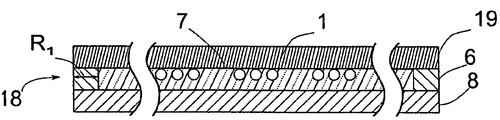
도 2는 본 발명에 따르는 두 번째 방법 단계에서의 제품 웨이퍼를 도시한다.
도 3은 본 발명에 따르는 세 번째 방법 단계에서의 제품 웨이퍼를 도시한다.
도 4는 본 발명에 따르는 네 번째 방법 단계에서의 제품 웨이퍼를 도시한다.
도 5는 본 발명에 따르는 다섯 번째 방법 단계에서의 제품 웨이퍼를 도시한다.
도 6은 본 발명에 따르는 여섯 번째 방법 단계에서의 제품 웨이퍼를 도시한다.
도 7은 본 발명에 따르는 일곱 번째 방법 단계에서의 제품 웨이퍼를 도시한다.
도 8은 본 발명에 따르는 여덟 번째 방법 단계에서의 제품 웨이퍼를 도시한다.
도 9는 본 발명에 따르는 아홉 번째 방법 단계에서의 제품 웨이퍼를 도시한다.
도 10은 본 발명에 따르는 열 번째 방법 단계에서의 제품 웨이퍼를 도시한다.
도 11은 본 발명에 따르는 대안적인 일곱 번째 방법 단계에서의 제품 웨이퍼를 도시한다.
도 12는 본 발명에 따르는 대안적인 일곱 번째 방법 단계에서의 제품 웨이퍼를 도시한다.
2 제 2 면
3 제 1 면
4 범프
5 범프 그룹
6 제 1 접착 층
7 필름
8 제 1 캐리어 웨이퍼
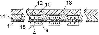
9 비아
10 범프
11 범프 그룹
12 칩
13 제 2 캐리어 웨이퍼
14 제 2 접착 층
15 칩
16 양면 장착 제품 웨이퍼
17, 17', 17" 제 2 중간 층
18, 18', 18" 제 1 중간 층
19 웨이퍼 둘레
29 광원
D 지름
H1 웨이퍼 두께
H2 웨이퍼 두께
R1, R1' 링 폭
R2, R2' 링 폭
B1 중간 층의 두께
B2 중간 층의 두께
Claims (16)
- 두 면에 칩이 제공되는 제품 웨이퍼를 제작하기 위한 방법에 있어서, 상기 방법은,
제품 웨이퍼의 제 1 면을, 제 1 중간 층을 포함하는 제 1 강성 캐리어 웨이퍼에 일시적으로 접합하는 단계 - 상기 제 1 중간 층은 제품 웨이퍼의 제 1 면의 적어도 변부(edge side)에 도포되는 하나의 제 1 접착 층을 포함하고, 상기 제 1 접착 층은 제 1 물질로 제조됨 - 와,
상기 제 1 면의 반대편에 있는 제품 웨이퍼의 제 2 면에 칩의 제공에 의해 상기 제 2 면을 가공하는 단계와,
제품 웨이퍼의 제 2 면을, 제 2 중간 층을 포함하는 제 2 강성 캐리어 웨이퍼에 접합하는 단계 - 상기 제 2 중간 층은 제품 웨이퍼의 제 2 면의 적어도 변부에 도포되는 하나의 제 2 접착 층을 포함하고, 상기 제 2 접착 층은 제 2 물질로 제조되며, 제 1 접착 층과 제 2 접착 층은 상이한 물질로 제조되어서, 제품 웨이퍼에 접합되는 두 강성 캐리어 웨이퍼 모두 제품 웨이퍼로부터 선택적으로 분리될 수 있음 - 와,
제 1 강성 캐리어 웨이퍼 및 제 2 강성 캐리어 웨이퍼 모두가 제품 웨이퍼에 접합한 후에, 제 1 강성 캐리어 웨이퍼, 제 2 강성 캐리어 웨이퍼 및 제품 웨이퍼의 조합물에 제 1 힘을 가하는 단계 - 제 1 강성 캐리어 웨이퍼 및 제 1 중간 층은 제품 웨이퍼로부터 분리됨 - 와,
제 1 강성 캐리어 웨이퍼 및 제 1 중간 층이 제품 웨이퍼로부터 분리된 후에, 제 2 강성 캐리어 웨이퍼에 제 2 힘을 가하는 단계 - 제 2 강성 캐리어 웨이퍼 및 제 2 중간 층은 제품 웨이퍼로부터 분리됨 - 를 포함하되, 상기 제 1 접착 층 및 상기 제 2 접착 층은 열가소성 시멘트로 제조된 것을 특징으로 하는 제품 웨이퍼를 제작하기 위한 방법. - 제 1 항에 있어서, 제 1 접착 층의 접합력(bonding force)은 제 2 접착 층의 접합력보다 작은 것을 특징으로 하는 제품 웨이퍼를 제작하기 위한 방법.
- 제 1 항에 있어서, 제 1 접착 층의 제품 웨이퍼 또는 제 1 강성 캐리어 웨이퍼와의 접촉 영역은, 제 2 접착 층의 제품 웨이퍼 또는 제 2 강성 캐리어 웨이퍼와의 접촉 영역보다 작은 것을 특징으로 하는 제품 웨이퍼를 제작하기 위한 방법.
- 제 1 항에 있어서, 제 1 힘을 가하는 단계는, 제 1 접착 층과 제 2 접착 층을 제 1 용매에 노출시키는 단계를 포함하되, 제 1 접착 층은 제 1 용매에 적어도 부분적으로 용해되는 반면, 제 2 접착 층은 제 1 용매에 대해 적어도 비활성화되는 것을 특징으로 하는 제품 웨이퍼를 제작하기 위한 방법.
- 제 1 항에 있어서, 제 1 힘을 가하는 단계는, 제 1 접착 층과 제 2 접착 층을 사전결정된 온도에 노출시키는 단계를 포함하되, 제 1 접착 층은 적어도 부분적으로 용해되고, 제 2 접착 층은 적어도 변하지 않아서, 제 2 강성 캐리어 웨이퍼의 분리 이전에 제 1 강성 캐리어 웨이퍼가 영향을 받는 것을 특징으로 하는 제품 웨이퍼를 제작하기 위한 방법.
- 제 1 항에 있어서, 제 1 힘을 가하는 단계는, 제 1 접착 층과 제 2 접착 층을 사전결정된 세기 또는 파장의 광원에 노출시키는 단계를 포함하되, 광원은 제 1 접착 층 또는 제 2 접착 층에 선택적으로 영향을 주는 것을 특징으로 하는 제품 웨이퍼를 제작하기 위한 방법.
- 제 1 항에 있어서, 제 1 접착 층의 전단 강도(shear strength)는 제 2 접착 층의 전단 강도보다 작은 것을 특징으로 하는 제품 웨이퍼를 제작하기 위한 방법.
- 제 1 항에 있어서, 제 1 접착 층 또는 제 2 접착 층은, 제품 웨이퍼의 둘레의 영역에서 환형으로 제조되는 것을 특징으로 하는 제품 웨이퍼를 제작하기 위한 방법.
- 제 1 항에 있어서, 제 1 강성 캐리어 웨이퍼와 제 1 중간 층 사이에, 제 1 강성 캐리어 웨이퍼에 도포되는 제 1 부분 코팅은 제 1 부분 코팅의 영역에서의 접합력/접착력을 감소시키도록 도포되거나, 제 2 강성 캐리어 웨이퍼와 제 2 접착 층 사이에, 제 2 강성 캐리어 웨이퍼에 도포되는 제 2 부분 코팅은 제 2 부분 코팅의 영역에서의 접합력/접착력을 감소시키도록 도포되는 것을 특징으로 하는 제품 웨이퍼를 제작하기 위한 방법.
- 두 면에 칩이 제공되는 제품 웨이퍼를 제작하기 위한 방법에 있어서, 상기 방법은,
제품 웨이퍼의 제 1 면을, 제 1 중간 층을 포함하는 제 1 강성 캐리어 웨이퍼에 일시적으로 접합하는 단계 - 상기 제 1 중간 층은 제품 웨이퍼의 제 1 면의 적어도 변부(edge side)에 도포되는 하나의 제 1 접착 층을 포함하고, 상기 제 1 접착 층은 제 1 물질로 제조됨 - 와,
상기 제 1 면의 반대편에 있는 제품 웨이퍼의 제 2 면에 칩의 제공에 의해 상기 제 2 면을 가공하는 단계와,
제품 웨이퍼의 제 2 면을, 제 2 중간 층을 포함하는 제 2 강성 캐리어 웨이퍼에 접합하는 단계 - 상기 제 2 중간 층은 제품 웨이퍼의 제 2 면의 적어도 변부에 도포되는 하나의 제 2 접착 층을 포함하고, 상기 제 2 접착 층은 제 2 물질로 제조되며, 제 1 접착 층의 제품 웨이퍼 또는 제 1 강성 캐리어 웨이퍼와의 접촉 영역은, 제 2 접착 층의 제품 웨이퍼 또는 제 2 강성 캐리어 웨이퍼와의 접촉 영역보다 작아서, 제품 웨이퍼에 접합되는 두 강성 캐리어 웨이퍼 모두 제품 웨이퍼로부터 선택적으로 분리될 수 있음 - 와,
제 1 강성 캐리어 웨이퍼 및 제 2 강성 캐리어 웨이퍼 모두가 제품 웨이퍼에 접합한 후에, 제 1 강성 캐리어 웨이퍼, 제 2 강성 캐리어 웨이퍼 및 제품 웨이퍼의 조합물에 제 1 힘을 가하는 단계 - 제 1 강성 캐리어 웨이퍼 및 제 1 중간 층은 제품 웨이퍼로부터 분리됨 - 와,
제 1 강성 캐리어 웨이퍼 및 제 1 중간 층이 제품 웨이퍼로부터 분리된 후에, 제 2 강성 캐리어 웨이퍼에 제 2 힘을 가하는 단계 - 제 2 강성 캐리어 웨이퍼 및 제 2 중간 층은 제품 웨이퍼로부터 분리됨 - 를 포함하되, 상기 제 1 접착 층 및 상기 제 2 접착 층은 열가소성 시멘트로 제조된 것을 특징으로 하는 제품 웨이퍼를 제작하기 위한 방법. - 제 10 항에 있어서, 제 1 접착 층 또는 제 2 접착 층은, 제품 웨이퍼의 둘레의 영역에서 환형으로 제조되는 것을 특징으로 하는 제품 웨이퍼를 제작하기 위한 방법.
- 제 10 항에 있어서, 제 1 물질과 제 2 물질은 동일한 것을 특징으로 하는 제품 웨이퍼를 제작하기 위한 방법.
- 두 면에 칩이 제공되는 제품 웨이퍼를 제작하기 위한 방법에 있어서, 상기 방법은,
제품 웨이퍼의 제 1 면을, 제 1 중간 층을 포함하는 제 1 강성 캐리어 웨이퍼에 일시적으로 접합하는 단계 - 상기 제 1 중간 층은 제품 웨이퍼의 제 1 면의 적어도 변부(edge side)에 도포되는 하나의 제 1 접착 층을 포함하고, 상기 제 1 접착 층은 제 1 물질로 제조됨 - 와,
상기 제 1 면의 반대편에 있는 제품 웨이퍼의 제 2 면에 칩의 제공에 의해 상기 제 2 면을 가공하는 단계와,
제품 웨이퍼의 제 2 면을, 제 2 중간 층을 포함하는 제 2 강성 캐리어 웨이퍼에 접합하는 단계 - 상기 제 2 중간 층은 제품 웨이퍼의 제 2 면의 적어도 변부에 도포되는 하나의 제 2 접착 층을 포함하고, 상기 제 2 접착 층은 제 2 물질로 제조되며, 제 1 접착 층의 두께는 제 2 접착 층의 두께보다 얇아서, 제품 웨이퍼에 접합되는 두 강성 캐리어 웨이퍼 모두 제품 웨이퍼로부터 선택적으로 분리될 수 있음 - 와,
제 1 강성 캐리어 웨이퍼 및 제 2 강성 캐리어 웨이퍼 모두가 제품 웨이퍼에 접합한 후에, 제 1 강성 캐리어 웨이퍼, 제 2 강성 캐리어 웨이퍼 및 제품 웨이퍼의 조합물에 제 1 힘을 가하는 단계 - 제 1 강성 캐리어 웨이퍼 및 제 1 중간 층은 제품 웨이퍼로부터 분리됨 - 와,
제 1 강성 캐리어 웨이퍼 및 제 1 중간 층이 제품 웨이퍼로부터 분리된 후에, 제 2 강성 캐리어 웨이퍼에 제 2 힘을 가하는 단계 - 제 2 강성 캐리어 웨이퍼 및 제 2 중간 층은 제품 웨이퍼로부터 분리됨 - 를 포함하되, 상기 제 1 접착 층 및 상기 제 2 접착 층은 열가소성 시멘트로 제조된 것을 특징으로 하는 제품 웨이퍼를 제작하기 위한 방법. - 제 13 항에 있어서, 제 1 접착 층 또는 제 2 접착 층은, 제품 웨이퍼의 둘레의 영역에서 환형으로 제조되는 것을 특징으로 하는 제품 웨이퍼를 제작하기 위한 방법.
- 제 13 항에 있어서, 제 1 물질과 제 2 물질은 동일한 것을 특징으로 하는 제품 웨이퍼를 제작하기 위한 방법.
- 제 11 항에 있어서, 제 2 접착 층의 링 폭(ring width)에 대한 제 1 접착 층의 링 폭의 비율은 1/10 내지 9/10 인 것을 특징으로 하는 제품 웨이퍼를 제작하기 위한 방법.
Applications Claiming Priority (1)
| Application Number | Priority Date | Filing Date | Title |
|---|---|---|---|
| PCT/EP2010/002055 WO2011120537A1 (de) | 2010-03-31 | 2010-03-31 | Verfahren zur herstellung eines doppelseitig mit chips bestückten wafers |
Related Parent Applications (1)
| Application Number | Title | Priority Date | Filing Date |
|---|---|---|---|
| KR1020167016168A Division KR20160075845A (ko) | 2010-03-31 | 2010-03-31 | 양면에 칩이 장착되는 웨이퍼를 제작하기 위한 방법 |
Publications (2)
| Publication Number | Publication Date |
|---|---|
| KR20170042817A KR20170042817A (ko) | 2017-04-19 |
| KR101856429B1 true KR101856429B1 (ko) | 2018-05-09 |
Family
ID=42286741
Family Applications (3)
| Application Number | Title | Priority Date | Filing Date |
|---|---|---|---|
| KR1020127023406A Ceased KR20130040779A (ko) | 2010-03-31 | 2010-03-31 | 양면에 칩이 장착되는 웨이퍼를 제작하기 위한 방법 |
| KR1020177009655A Active KR101856429B1 (ko) | 2010-03-31 | 2010-03-31 | 양면에 칩이 장착되는 웨이퍼를 제작하기 위한 방법 |
| KR1020167016168A Ceased KR20160075845A (ko) | 2010-03-31 | 2010-03-31 | 양면에 칩이 장착되는 웨이퍼를 제작하기 위한 방법 |
Family Applications Before (1)
| Application Number | Title | Priority Date | Filing Date |
|---|---|---|---|
| KR1020127023406A Ceased KR20130040779A (ko) | 2010-03-31 | 2010-03-31 | 양면에 칩이 장착되는 웨이퍼를 제작하기 위한 방법 |
Family Applications After (1)
| Application Number | Title | Priority Date | Filing Date |
|---|---|---|---|
| KR1020167016168A Ceased KR20160075845A (ko) | 2010-03-31 | 2010-03-31 | 양면에 칩이 장착되는 웨이퍼를 제작하기 위한 방법 |
Country Status (8)
| Country | Link |
|---|---|
| US (1) | US9224630B2 (ko) |
| EP (1) | EP2553719B1 (ko) |
| JP (1) | JP5763169B2 (ko) |
| KR (3) | KR20130040779A (ko) |
| CN (1) | CN102812546B (ko) |
| SG (1) | SG183820A1 (ko) |
| TW (1) | TWI518758B (ko) |
| WO (1) | WO2011120537A1 (ko) |
Families Citing this family (8)
| Publication number | Priority date | Publication date | Assignee | Title |
|---|---|---|---|---|
| US9827757B2 (en) | 2011-07-07 | 2017-11-28 | Brewer Science Inc. | Methods of transferring device wafers or layers between carrier substrates and other surfaces |
| EP3130069B1 (en) * | 2014-04-09 | 2022-11-16 | Lionel O. Barthold | Multi-module dc-to-dc power transformation system |
| WO2020178080A1 (en) * | 2019-03-05 | 2020-09-10 | Evatec Ag | Method for processing fragile substrates employing temporary bonding of the substrates to carriers |
| WO2021164855A1 (de) | 2020-02-18 | 2021-08-26 | Ev Group E. Thallner Gmbh | Verfahren und vorrichtung zur übertragung von bauteilen |
| KR20240166455A (ko) | 2022-03-25 | 2024-11-26 | 에베 그룹 에. 탈너 게엠베하 | 캐리어 기판 분리 방법 및 기판 시스템 |
| KR102788502B1 (ko) * | 2023-07-27 | 2025-04-01 | 한국기계연구원 | 효과적인 디본딩이 가능한 웨이퍼 모듈, 및 이의 본딩 및 디본딩 방법 |
| WO2025228530A1 (de) | 2024-05-02 | 2025-11-06 | Ev Group E. Thallner Gmbh | Verfahren zum temporären verbinden eines produktsubstrats und eines trägersubstrats, trägersubstrat, produktsubstrat und schichtsystem sowie deren anordnung und eine vorrichtung zum durchführen eines solchen verfahrens |
| WO2026104042A1 (de) | 2024-11-14 | 2026-05-21 | Ev Group E. Thallner Gmbh | Verfahren zum temporären verbinden und lösen eines produktsubstrats und eines trägersubstrats und eine vorrichtung für ein solches verfahren |
Citations (4)
| Publication number | Priority date | Publication date | Assignee | Title |
|---|---|---|---|---|
| US20050029224A1 (en) * | 2001-04-13 | 2005-02-10 | Bernard Aspar | Detachable substrate or detachable structure and method for the production thereof |
| US20080003780A1 (en) * | 2006-06-30 | 2008-01-03 | Haixiao Sun | Detachable stiffener for ultra-thin die |
| JP2009043962A (ja) * | 2007-08-09 | 2009-02-26 | Sony Corp | 半導体装置の製造方法 |
| US20090218560A1 (en) * | 2008-01-24 | 2009-09-03 | Brewer Science Inc. | Method for reversibly mounting a device wafer to a carrier substrate |
Family Cites Families (35)
| Publication number | Priority date | Publication date | Assignee | Title |
|---|---|---|---|---|
| JPS6198784A (ja) * | 1984-10-20 | 1986-05-17 | Kimurashin Kk | ロール状又は積層状の両面接着テープ |
| JPH04283283A (ja) * | 1991-03-08 | 1992-10-08 | Nippon Synthetic Chem Ind Co Ltd:The | 開封自在テープ |
| JP3686454B2 (ja) * | 1995-05-10 | 2005-08-24 | 日東電工株式会社 | 接着型使捨てカイロ用粘着シート及びそのカイロ |
| WO1997039481A1 (en) * | 1996-04-12 | 1997-10-23 | Northeastern University | An integrated complex-transition metal oxide device and a method of fabricating such a device |
| JPH11105924A (ja) * | 1997-10-06 | 1999-04-20 | Nitto Denko Corp | 電子部品搬送用テ−プ |
| JPH11238375A (ja) * | 1998-02-20 | 1999-08-31 | Sony Corp | 電子機器の放熱装置とディスクドライブ装置 |
| JP2000326995A (ja) * | 1999-05-17 | 2000-11-28 | Ogawa Sangyo Kk | 滅菌袋 |
| JP2002097041A (ja) * | 2000-07-17 | 2002-04-02 | Sekisui Chem Co Ltd | 合わせガラス用中間膜及び合わせガラス |
| JP3861669B2 (ja) * | 2001-11-22 | 2006-12-20 | ソニー株式会社 | マルチチップ回路モジュールの製造方法 |
| JP2003218063A (ja) * | 2002-01-24 | 2003-07-31 | Canon Inc | ウエハ貼着用粘着シート及び該シートを利用する加工方法 |
| US6794273B2 (en) | 2002-05-24 | 2004-09-21 | Fujitsu Limited | Semiconductor device and manufacturing method thereof |
| JP4565804B2 (ja) | 2002-06-03 | 2010-10-20 | スリーエム イノベイティブ プロパティズ カンパニー | 被研削基材を含む積層体、その製造方法並びに積層体を用いた極薄基材の製造方法及びそのための装置 |
| JP4364535B2 (ja) | 2003-03-27 | 2009-11-18 | シャープ株式会社 | 半導体装置の製造方法 |
| JP4405246B2 (ja) | 2003-11-27 | 2010-01-27 | スリーエム イノベイティブ プロパティズ カンパニー | 半導体チップの製造方法 |
| US7232740B1 (en) * | 2005-05-16 | 2007-06-19 | The United States Of America As Represented By The National Security Agency | Method for bumping a thin wafer |
| US8592286B2 (en) * | 2005-10-05 | 2013-11-26 | Stats Chippac Ltd. | Ultra-thin wafer system and method of manufacture thereof |
| DE102006000687B4 (de) | 2006-01-03 | 2010-09-09 | Thallner, Erich, Dipl.-Ing. | Kombination aus einem Träger und einem Wafer, Vorrichtung zum Trennen der Kombination und Verfahren zur Handhabung eines Trägers und eines Wafers |
| US20080044984A1 (en) * | 2006-08-16 | 2008-02-21 | Taiwan Semiconductor Manufacturing Co., Ltd. | Methods of avoiding wafer breakage during manufacture of backside illuminated image sensors |
| US7838391B2 (en) * | 2007-05-07 | 2010-11-23 | Stats Chippac, Ltd. | Ultra thin bumped wafer with under-film |
| EP2104138A1 (de) | 2008-03-18 | 2009-09-23 | EV Group E. Thallner GmbH | Verfahren zum Bonden von Chips auf Wafer |
| JP4572243B2 (ja) * | 2008-03-27 | 2010-11-04 | 信越化学工業株式会社 | 熱伝導性積層体およびその製造方法 |
| JP2010010644A (ja) * | 2008-05-27 | 2010-01-14 | Toshiba Corp | 半導体装置の製造方法 |
| JP2010092931A (ja) * | 2008-10-03 | 2010-04-22 | Toshiba Corp | 半導体装置の製造方法及び半導体装置の製造装置 |
| WO2010121068A2 (en) | 2009-04-16 | 2010-10-21 | Suss Microtec, Inc. | Improved apparatus for temporary wafer bonding and debonding |
| US8689437B2 (en) * | 2009-06-24 | 2014-04-08 | International Business Machines Corporation | Method for forming integrated circuit assembly |
| EP2299486B1 (de) * | 2009-09-18 | 2015-02-18 | EV Group E. Thallner GmbH | Verfahren zum Bonden von Chips auf Wafer |
| US8008121B2 (en) * | 2009-11-04 | 2011-08-30 | Stats Chippac, Ltd. | Semiconductor package and method of mounting semiconductor die to opposite sides of TSV substrate |
| US9136144B2 (en) * | 2009-11-13 | 2015-09-15 | Stats Chippac, Ltd. | Method of forming protective material between semiconductor die stacked on semiconductor wafer to reduce defects during singulation |
| US8017439B2 (en) * | 2010-01-26 | 2011-09-13 | Texas Instruments Incorporated | Dual carrier for joining IC die or wafers to TSV wafers |
| TWI419302B (zh) * | 2010-02-11 | 2013-12-11 | 日月光半導體製造股份有限公司 | 封裝製程 |
| US8252682B2 (en) * | 2010-02-12 | 2012-08-28 | Taiwan Semiconductor Manufacturing Company, Ltd. | Method for thinning a wafer |
| JP4976522B2 (ja) * | 2010-04-16 | 2012-07-18 | 日東電工株式会社 | 熱硬化型ダイボンドフィルム、ダイシング・ダイボンドフィルム、及び、半導体装置の製造方法 |
| US8852391B2 (en) * | 2010-06-21 | 2014-10-07 | Brewer Science Inc. | Method and apparatus for removing a reversibly mounted device wafer from a carrier substrate |
| US8492197B2 (en) * | 2010-08-17 | 2013-07-23 | Stats Chippac, Ltd. | Semiconductor device and method of forming vertically offset conductive pillars over first substrate aligned to vertically offset BOT interconnect sites formed over second substrate |
| JP2012069919A (ja) * | 2010-08-25 | 2012-04-05 | Toshiba Corp | 半導体装置の製造方法 |
-
2010
- 2010-03-31 WO PCT/EP2010/002055 patent/WO2011120537A1/de not_active Ceased
- 2010-03-31 JP JP2013501635A patent/JP5763169B2/ja active Active
- 2010-03-31 US US13/635,457 patent/US9224630B2/en active Active
- 2010-03-31 KR KR1020127023406A patent/KR20130040779A/ko not_active Ceased
- 2010-03-31 KR KR1020177009655A patent/KR101856429B1/ko active Active
- 2010-03-31 EP EP10715497.3A patent/EP2553719B1/de active Active
- 2010-03-31 KR KR1020167016168A patent/KR20160075845A/ko not_active Ceased
- 2010-03-31 SG SG2012063681A patent/SG183820A1/en unknown
- 2010-03-31 CN CN201080065914.6A patent/CN102812546B/zh active Active
-
2011
- 2011-02-25 TW TW100106549A patent/TWI518758B/zh active
Patent Citations (4)
| Publication number | Priority date | Publication date | Assignee | Title |
|---|---|---|---|---|
| US20050029224A1 (en) * | 2001-04-13 | 2005-02-10 | Bernard Aspar | Detachable substrate or detachable structure and method for the production thereof |
| US20080003780A1 (en) * | 2006-06-30 | 2008-01-03 | Haixiao Sun | Detachable stiffener for ultra-thin die |
| JP2009043962A (ja) * | 2007-08-09 | 2009-02-26 | Sony Corp | 半導体装置の製造方法 |
| US20090218560A1 (en) * | 2008-01-24 | 2009-09-03 | Brewer Science Inc. | Method for reversibly mounting a device wafer to a carrier substrate |
Also Published As
| Publication number | Publication date |
|---|---|
| KR20130040779A (ko) | 2013-04-24 |
| JP5763169B2 (ja) | 2015-08-12 |
| WO2011120537A1 (de) | 2011-10-06 |
| KR20170042817A (ko) | 2017-04-19 |
| JP2013524493A (ja) | 2013-06-17 |
| TWI518758B (zh) | 2016-01-21 |
| EP2553719A1 (de) | 2013-02-06 |
| US20130011997A1 (en) | 2013-01-10 |
| US9224630B2 (en) | 2015-12-29 |
| SG183820A1 (en) | 2012-10-30 |
| CN102812546B (zh) | 2015-08-26 |
| TW201145370A (en) | 2011-12-16 |
| EP2553719B1 (de) | 2019-12-04 |
| KR20160075845A (ko) | 2016-06-29 |
| CN102812546A (zh) | 2012-12-05 |
Similar Documents
| Publication | Publication Date | Title |
|---|---|---|
| KR20170042817A (ko) | 양면에 칩이 장착되는 웨이퍼를 제작하기 위한 방법 | |
| TWI446420B (zh) | 用於半導體製程之載體分離方法 | |
| CN101764047B (zh) | 减薄半导体衬底的方法 | |
| US7226812B2 (en) | Wafer support and release in wafer processing | |
| JP4762671B2 (ja) | ダイシングテープ、および半導体ウェハダイシング方法 | |
| US7462551B2 (en) | Adhesive system for supporting thin silicon wafer | |
| US8846499B2 (en) | Composite carrier structure | |
| KR102061369B1 (ko) | 제품 기판을 캐리어 기판에 임시로 결합하기 위한 방법 | |
| JP2008521214A (ja) | 半導体ウエハの薄型化 | |
| JP2019514199A (ja) | 2枚の基板を接合する方法および装置 | |
| JP7728241B2 (ja) | 保護膜形成用シート、保護膜付きチップの製造方法、及び積層物 | |
| TW200426907A (en) | Fabrication method of semiconductor device | |
| JP6457223B2 (ja) | 基板分離方法および半導体製造装置 | |
| JP2008028325A (ja) | 半導体装置の製造方法 | |
| JP2018088492A (ja) | 被加工物の固定方法、及び被加工物の加工方法 | |
| KR100759687B1 (ko) | 기판의 박판화 방법 및 회로소자의 제조방법 | |
| TW201921545A (zh) | 基板處理系統及基板處理方法 | |
| JP2005277103A (ja) | 半導体ウェハ、支持体および半導体ウェハ製造方法ならびにスペーサ製造方法および半導体素子製造方法 | |
| CN118737958A (zh) | 半导体器件及其制作方法 | |
| JP2008034644A (ja) | 剥離方法 | |
| JPH05109679A (ja) | 半導体装置の製造方法 | |
| TWI509739B (zh) | 半導體裝置的製造方法 | |
| JP2026064484A (ja) | 加工方法 | |
| CN121058079A (zh) | 半导体装置的制造方法及半导体装置 | |
| CN120858437A (zh) | 半导体装置的制造方法及切割带 |
Legal Events
| Date | Code | Title | Description |
|---|---|---|---|
| A107 | Divisional application of patent | ||
| A201 | Request for examination | ||
| PA0104 | Divisional application for international application |
St.27 status event code: A-0-1-A10-A18-div-PA0104 St.27 status event code: A-0-1-A10-A16-div-PA0104 |
|
| PA0201 | Request for examination |
St.27 status event code: A-1-2-D10-D11-exm-PA0201 |
|
| PG1501 | Laying open of application |
St.27 status event code: A-1-1-Q10-Q12-nap-PG1501 |
|
| E902 | Notification of reason for refusal | ||
| PE0902 | Notice of grounds for rejection |
St.27 status event code: A-1-2-D10-D21-exm-PE0902 |
|
| R17-X000 | Change to representative recorded |
St.27 status event code: A-3-3-R10-R17-oth-X000 |
|
| E601 | Decision to refuse application | ||
| PE0601 | Decision on rejection of patent |
St.27 status event code: N-2-6-B10-B15-exm-PE0601 |
|
| T11-X000 | Administrative time limit extension requested |
St.27 status event code: U-3-3-T10-T11-oth-X000 |
|
| T13-X000 | Administrative time limit extension granted |
St.27 status event code: U-3-3-T10-T13-oth-X000 |
|
| T13-X000 | Administrative time limit extension granted |
St.27 status event code: U-3-3-T10-T13-oth-X000 |
|
| AMND | Amendment | ||
| P11-X000 | Amendment of application requested |
St.27 status event code: A-2-2-P10-P11-nap-X000 |
|
| P13-X000 | Application amended |
St.27 status event code: A-2-2-P10-P13-nap-X000 |
|
| PX0901 | Re-examination |
St.27 status event code: A-2-3-E10-E12-rex-PX0901 |
|
| PX0701 | Decision of registration after re-examination |
St.27 status event code: A-3-4-F10-F13-rex-PX0701 |
|
| X701 | Decision to grant (after re-examination) | ||
| GRNT | Written decision to grant | ||
| PR0701 | Registration of establishment |
St.27 status event code: A-2-4-F10-F11-exm-PR0701 |
|
| PR1002 | Payment of registration fee |
St.27 status event code: A-2-2-U10-U12-oth-PR1002 Fee payment year number: 1 |
|
| PG1601 | Publication of registration |
St.27 status event code: A-4-4-Q10-Q13-nap-PG1601 |
|
| PR1001 | Payment of annual fee |
St.27 status event code: A-4-4-U10-U11-oth-PR1001 Fee payment year number: 4 |
|
| PR1001 | Payment of annual fee |
St.27 status event code: A-4-4-U10-U11-oth-PR1001 Fee payment year number: 5 |
|
| PR1001 | Payment of annual fee |
St.27 status event code: A-4-4-U10-U11-oth-PR1001 Fee payment year number: 6 |
|
| PR1001 | Payment of annual fee |
St.27 status event code: A-4-4-U10-U11-oth-PR1001 Fee payment year number: 7 |
|
| PR1001 | Payment of annual fee |
St.27 status event code: A-4-4-U10-U11-oth-PR1001 Fee payment year number: 8 |
|
| P22-X000 | Classification modified |
St.27 status event code: A-4-4-P10-P22-nap-X000 |