KR101856429B1 - Method for producing a wafer equipped with chips on two sides - Google Patents
Method for producing a wafer equipped with chips on two sides Download PDFInfo
- Publication number
- KR101856429B1 KR101856429B1 KR1020177009655A KR20177009655A KR101856429B1 KR 101856429 B1 KR101856429 B1 KR 101856429B1 KR 1020177009655 A KR1020177009655 A KR 1020177009655A KR 20177009655 A KR20177009655 A KR 20177009655A KR 101856429 B1 KR101856429 B1 KR 101856429B1
- Authority
- KR
- South Korea
- Prior art keywords
- wafer
- adhesive layer
- rigid carrier
- product wafer
- product
- Prior art date
- Legal status (The legal status is an assumption and is not a legal conclusion. Google has not performed a legal analysis and makes no representation as to the accuracy of the status listed.)
- Active
Links
Images





Classifications
-
- H—ELECTRICITY
- H10—SEMICONDUCTOR DEVICES; ELECTRIC SOLID-STATE DEVICES NOT OTHERWISE PROVIDED FOR
- H10P—GENERIC PROCESSES OR APPARATUS FOR THE MANUFACTURE OR TREATMENT OF DEVICES COVERED BY CLASS H10
- H10P72/00—Handling or holding of wafers, substrates or devices during manufacture or treatment thereof
- H10P72/70—Handling or holding of wafers, substrates or devices during manufacture or treatment thereof for supporting or gripping
- H10P72/74—Handling or holding of wafers, substrates or devices during manufacture or treatment thereof for supporting or gripping using temporarily an auxiliary support
-
- H—ELECTRICITY
- H10—SEMICONDUCTOR DEVICES; ELECTRIC SOLID-STATE DEVICES NOT OTHERWISE PROVIDED FOR
- H10P—GENERIC PROCESSES OR APPARATUS FOR THE MANUFACTURE OR TREATMENT OF DEVICES COVERED BY CLASS H10
- H10P72/00—Handling or holding of wafers, substrates or devices during manufacture or treatment thereof
- H10P72/50—Handling or holding of wafers, substrates or devices during manufacture or treatment thereof for positioning, orientation or alignment
-
- H01L21/68—
-
- H01L21/185—
-
- H01L23/31—
-
- H—ELECTRICITY
- H10—SEMICONDUCTOR DEVICES; ELECTRIC SOLID-STATE DEVICES NOT OTHERWISE PROVIDED FOR
- H10P—GENERIC PROCESSES OR APPARATUS FOR THE MANUFACTURE OR TREATMENT OF DEVICES COVERED BY CLASS H10
- H10P10/00—Bonding of wafers, substrates or parts of devices
- H10P10/12—Bonding of semiconductor wafers or semiconductor substrates to semiconductor wafers or semiconductor substrates
-
- H—ELECTRICITY
- H10—SEMICONDUCTOR DEVICES; ELECTRIC SOLID-STATE DEVICES NOT OTHERWISE PROVIDED FOR
- H10W—GENERIC PACKAGES, INTERCONNECTIONS, CONNECTORS OR OTHER CONSTRUCTIONAL DETAILS OF DEVICES COVERED BY CLASS H10
- H10W74/00—Encapsulations, e.g. protective coatings
- H10W74/10—Encapsulations, e.g. protective coatings characterised by their shape or disposition
-
- H—ELECTRICITY
- H10—SEMICONDUCTOR DEVICES; ELECTRIC SOLID-STATE DEVICES NOT OTHERWISE PROVIDED FOR
- H10W—GENERIC PACKAGES, INTERCONNECTIONS, CONNECTORS OR OTHER CONSTRUCTIONAL DETAILS OF DEVICES COVERED BY CLASS H10
- H10W90/00—Package configurations
-
- H—ELECTRICITY
- H10—SEMICONDUCTOR DEVICES; ELECTRIC SOLID-STATE DEVICES NOT OTHERWISE PROVIDED FOR
- H10P—GENERIC PROCESSES OR APPARATUS FOR THE MANUFACTURE OR TREATMENT OF DEVICES COVERED BY CLASS H10
- H10P72/00—Handling or holding of wafers, substrates or devices during manufacture or treatment thereof
- H10P72/70—Handling or holding of wafers, substrates or devices during manufacture or treatment thereof for supporting or gripping
- H10P72/74—Handling or holding of wafers, substrates or devices during manufacture or treatment thereof for supporting or gripping using temporarily an auxiliary support
- H10P72/7412—Handling or holding of wafers, substrates or devices during manufacture or treatment thereof for supporting or gripping using temporarily an auxiliary support the auxiliary support including means facilitating the separation of a device or wafer from the auxiliary support
-
- H—ELECTRICITY
- H10—SEMICONDUCTOR DEVICES; ELECTRIC SOLID-STATE DEVICES NOT OTHERWISE PROVIDED FOR
- H10P—GENERIC PROCESSES OR APPARATUS FOR THE MANUFACTURE OR TREATMENT OF DEVICES COVERED BY CLASS H10
- H10P72/00—Handling or holding of wafers, substrates or devices during manufacture or treatment thereof
- H10P72/70—Handling or holding of wafers, substrates or devices during manufacture or treatment thereof for supporting or gripping
- H10P72/74—Handling or holding of wafers, substrates or devices during manufacture or treatment thereof for supporting or gripping using temporarily an auxiliary support
- H10P72/7416—Handling or holding of wafers, substrates or devices during manufacture or treatment thereof for supporting or gripping using temporarily an auxiliary support used during dicing or grinding
- H10P72/7418—Handling or holding of wafers, substrates or devices during manufacture or treatment thereof for supporting or gripping using temporarily an auxiliary support used during dicing or grinding of passive members, e.g. a chip mounting substrate
-
- H—ELECTRICITY
- H10—SEMICONDUCTOR DEVICES; ELECTRIC SOLID-STATE DEVICES NOT OTHERWISE PROVIDED FOR
- H10P—GENERIC PROCESSES OR APPARATUS FOR THE MANUFACTURE OR TREATMENT OF DEVICES COVERED BY CLASS H10
- H10P72/00—Handling or holding of wafers, substrates or devices during manufacture or treatment thereof
- H10P72/70—Handling or holding of wafers, substrates or devices during manufacture or treatment thereof for supporting or gripping
- H10P72/74—Handling or holding of wafers, substrates or devices during manufacture or treatment thereof for supporting or gripping using temporarily an auxiliary support
- H10P72/7436—Handling or holding of wafers, substrates or devices during manufacture or treatment thereof for supporting or gripping using temporarily an auxiliary support used to support a device or a wafer when forming electrical connections thereto
-
- H—ELECTRICITY
- H10—SEMICONDUCTOR DEVICES; ELECTRIC SOLID-STATE DEVICES NOT OTHERWISE PROVIDED FOR
- H10P—GENERIC PROCESSES OR APPARATUS FOR THE MANUFACTURE OR TREATMENT OF DEVICES COVERED BY CLASS H10
- H10P72/00—Handling or holding of wafers, substrates or devices during manufacture or treatment thereof
- H10P72/70—Handling or holding of wafers, substrates or devices during manufacture or treatment thereof for supporting or gripping
- H10P72/74—Handling or holding of wafers, substrates or devices during manufacture or treatment thereof for supporting or gripping using temporarily an auxiliary support
- H10P72/744—Details of chemical or physical process used for separating the auxiliary support from a device or a wafer
-
- H—ELECTRICITY
- H10—SEMICONDUCTOR DEVICES; ELECTRIC SOLID-STATE DEVICES NOT OTHERWISE PROVIDED FOR
- H10P—GENERIC PROCESSES OR APPARATUS FOR THE MANUFACTURE OR TREATMENT OF DEVICES COVERED BY CLASS H10
- H10P72/00—Handling or holding of wafers, substrates or devices during manufacture or treatment thereof
- H10P72/70—Handling or holding of wafers, substrates or devices during manufacture or treatment thereof for supporting or gripping
- H10P72/74—Handling or holding of wafers, substrates or devices during manufacture or treatment thereof for supporting or gripping using temporarily an auxiliary support
- H10P72/744—Details of chemical or physical process used for separating the auxiliary support from a device or a wafer
- H10P72/7442—Separation by peeling
-
- H—ELECTRICITY
- H10—SEMICONDUCTOR DEVICES; ELECTRIC SOLID-STATE DEVICES NOT OTHERWISE PROVIDED FOR
- H10P—GENERIC PROCESSES OR APPARATUS FOR THE MANUFACTURE OR TREATMENT OF DEVICES COVERED BY CLASS H10
- H10P72/00—Handling or holding of wafers, substrates or devices during manufacture or treatment thereof
- H10P72/70—Handling or holding of wafers, substrates or devices during manufacture or treatment thereof for supporting or gripping
- H10P72/74—Handling or holding of wafers, substrates or devices during manufacture or treatment thereof for supporting or gripping using temporarily an auxiliary support
- H10P72/744—Details of chemical or physical process used for separating the auxiliary support from a device or a wafer
- H10P72/7442—Separation by peeling
- H10P72/7444—Separation by peeling using a peeling wedge, a knife or a bar
-
- H—ELECTRICITY
- H10—SEMICONDUCTOR DEVICES; ELECTRIC SOLID-STATE DEVICES NOT OTHERWISE PROVIDED FOR
- H10W—GENERIC PACKAGES, INTERCONNECTIONS, CONNECTORS OR OTHER CONSTRUCTIONAL DETAILS OF DEVICES COVERED BY CLASS H10
- H10W70/00—Package substrates; Interposers; Redistribution layers [RDL]
- H10W70/01—Manufacture or treatment
- H10W70/05—Manufacture or treatment of insulating or insulated package substrates, or of interposers, or of redistribution layers
- H10W70/095—Manufacture or treatment of insulating or insulated package substrates, or of interposers, or of redistribution layers of vias therein
-
- H—ELECTRICITY
- H10—SEMICONDUCTOR DEVICES; ELECTRIC SOLID-STATE DEVICES NOT OTHERWISE PROVIDED FOR
- H10W—GENERIC PACKAGES, INTERCONNECTIONS, CONNECTORS OR OTHER CONSTRUCTIONAL DETAILS OF DEVICES COVERED BY CLASS H10
- H10W70/00—Package substrates; Interposers; Redistribution layers [RDL]
- H10W70/60—Insulating or insulated package substrates; Interposers; Redistribution layers
- H10W70/611—Insulating or insulated package substrates; Interposers; Redistribution layers for connecting multiple chips together
-
- H—ELECTRICITY
- H10—SEMICONDUCTOR DEVICES; ELECTRIC SOLID-STATE DEVICES NOT OTHERWISE PROVIDED FOR
- H10W—GENERIC PACKAGES, INTERCONNECTIONS, CONNECTORS OR OTHER CONSTRUCTIONAL DETAILS OF DEVICES COVERED BY CLASS H10
- H10W70/00—Package substrates; Interposers; Redistribution layers [RDL]
- H10W70/60—Insulating or insulated package substrates; Interposers; Redistribution layers
- H10W70/62—Insulating or insulated package substrates; Interposers; Redistribution layers characterised by their interconnections
- H10W70/63—Vias, e.g. via plugs
- H10W70/635—Through-vias
-
- H—ELECTRICITY
- H10—SEMICONDUCTOR DEVICES; ELECTRIC SOLID-STATE DEVICES NOT OTHERWISE PROVIDED FOR
- H10W—GENERIC PACKAGES, INTERCONNECTIONS, CONNECTORS OR OTHER CONSTRUCTIONAL DETAILS OF DEVICES COVERED BY CLASS H10
- H10W72/00—Interconnections or connectors in packages
- H10W72/01—Manufacture or treatment
- H10W72/0198—Manufacture or treatment batch processes
-
- H—ELECTRICITY
- H10—SEMICONDUCTOR DEVICES; ELECTRIC SOLID-STATE DEVICES NOT OTHERWISE PROVIDED FOR
- H10W—GENERIC PACKAGES, INTERCONNECTIONS, CONNECTORS OR OTHER CONSTRUCTIONAL DETAILS OF DEVICES COVERED BY CLASS H10
- H10W72/00—Interconnections or connectors in packages
- H10W72/071—Connecting or disconnecting
- H10W72/072—Connecting or disconnecting of bump connectors
-
- H—ELECTRICITY
- H10—SEMICONDUCTOR DEVICES; ELECTRIC SOLID-STATE DEVICES NOT OTHERWISE PROVIDED FOR
- H10W—GENERIC PACKAGES, INTERCONNECTIONS, CONNECTORS OR OTHER CONSTRUCTIONAL DETAILS OF DEVICES COVERED BY CLASS H10
- H10W72/00—Interconnections or connectors in packages
- H10W72/071—Connecting or disconnecting
- H10W72/072—Connecting or disconnecting of bump connectors
- H10W72/07202—Connecting or disconnecting of bump connectors using auxiliary members
- H10W72/07204—Connecting or disconnecting of bump connectors using auxiliary members using temporary auxiliary members, e.g. sacrificial coatings
- H10W72/07207—Temporary substrates, e.g. removable substrates
-
- H—ELECTRICITY
- H10—SEMICONDUCTOR DEVICES; ELECTRIC SOLID-STATE DEVICES NOT OTHERWISE PROVIDED FOR
- H10W—GENERIC PACKAGES, INTERCONNECTIONS, CONNECTORS OR OTHER CONSTRUCTIONAL DETAILS OF DEVICES COVERED BY CLASS H10
- H10W72/00—Interconnections or connectors in packages
- H10W72/20—Bump connectors, e.g. solder bumps or copper pillars; Dummy bumps; Thermal bumps
- H10W72/241—Dispositions, e.g. layouts
-
- H—ELECTRICITY
- H10—SEMICONDUCTOR DEVICES; ELECTRIC SOLID-STATE DEVICES NOT OTHERWISE PROVIDED FOR
- H10W—GENERIC PACKAGES, INTERCONNECTIONS, CONNECTORS OR OTHER CONSTRUCTIONAL DETAILS OF DEVICES COVERED BY CLASS H10
- H10W74/00—Encapsulations, e.g. protective coatings
- H10W74/01—Manufacture or treatment
- H10W74/014—Manufacture or treatment using batch processing
-
- H—ELECTRICITY
- H10—SEMICONDUCTOR DEVICES; ELECTRIC SOLID-STATE DEVICES NOT OTHERWISE PROVIDED FOR
- H10W—GENERIC PACKAGES, INTERCONNECTIONS, CONNECTORS OR OTHER CONSTRUCTIONAL DETAILS OF DEVICES COVERED BY CLASS H10
- H10W90/00—Package configurations
- H10W90/20—Configurations of stacked chips
- H10W90/22—Configurations of stacked chips the stacked chips being on both top and bottom sides of a package substrate, interposer or RDL
-
- H—ELECTRICITY
- H10—SEMICONDUCTOR DEVICES; ELECTRIC SOLID-STATE DEVICES NOT OTHERWISE PROVIDED FOR
- H10W—GENERIC PACKAGES, INTERCONNECTIONS, CONNECTORS OR OTHER CONSTRUCTIONAL DETAILS OF DEVICES COVERED BY CLASS H10
- H10W90/00—Package configurations
- H10W90/20—Configurations of stacked chips
- H10W90/297—Configurations of stacked chips characterised by the through-semiconductor vias [TSVs] in the stacked chips
-
- H—ELECTRICITY
- H10—SEMICONDUCTOR DEVICES; ELECTRIC SOLID-STATE DEVICES NOT OTHERWISE PROVIDED FOR
- H10W—GENERIC PACKAGES, INTERCONNECTIONS, CONNECTORS OR OTHER CONSTRUCTIONAL DETAILS OF DEVICES COVERED BY CLASS H10
- H10W90/00—Package configurations
- H10W90/701—Package configurations characterised by the relative positions of pads or connectors relative to package parts
- H10W90/721—Package configurations characterised by the relative positions of pads or connectors relative to package parts of bump connectors
- H10W90/724—Package configurations characterised by the relative positions of pads or connectors relative to package parts of bump connectors between a chip and a stacked insulating package substrate, interposer or RDL
Landscapes
- Container, Conveyance, Adherence, Positioning, Of Wafer (AREA)
- Mechanical Treatment Of Semiconductor (AREA)
- Engineering & Computer Science (AREA)
- Manufacturing & Machinery (AREA)
- Pressure Welding/Diffusion-Bonding (AREA)
Abstract
본 발명은 칩(12, 15)이 양면에 장착되는 제품 웨이퍼(1)를 제작하기 위한 방법에 관한 것이며, 상기 방법은, 특히, 제품 웨이퍼의 제 1 면(3)을 가공하는 단계와, 제품 웨이퍼(1)의 제 1 면(3)을, 적어도 변부에 제공되는 하나의 제 1 접착 층(6)으로 구성된 제 1 중간 층(18)을 갖는 제 1 강성 캐리어 웨이퍼(8)로 접합하는 단계와, 상기 제 1 면(3)의 반대편의 제품 웨이퍼(1)의 제 2 면(2)을 가공하는 단계, 제품 웨이퍼(1)의 제 2 면(2)을, 적어도 변부 측에 제공되는 하나의 제 2 접착 층(14)으로 구성된 제 2 중간 층(17)을 갖는 제 2 강성 캐리어 웨이퍼(13)로 접합하는 단계를 포함하며, 제 2 캐리어 웨이퍼(13)보다 먼저 제 1 캐리어 웨이퍼(8)가 선택적으로 분리될 수 있도록 제 1 중간 층(18)과 제 2 중간 층(17)은 상이하게 만들어진다.The invention relates to a method for manufacturing a product wafer (1) on which chips (12, 15) are mounted on both sides, the method comprising the steps of: machining a first side (3) Bonding the first side 3 of the wafer 1 to a first rigid carrier wafer 8 having a first intermediate layer 18 composed of at least one first adhesive layer 6 provided on the side edge, ; Machining the second side (2) of the product wafer (1) opposite the first side (3), the second side (2) of the product wafer (1) With a second rigid carrier wafer (13) having a second intermediate layer (17) comprised of a second adhesive layer (14) of a first carrier wafer (8) The first intermediate layer 18 and the second intermediate layer 17 are made different from each other.
Description
본 발명은 청구항 1에서 청구되는 바와 같이, 특히, 양면에 칩(chip)이 제공되는 제품 웨이퍼(product wafer)를 제작하기 위한 방법에 관한 것이다.The present invention relates to a method for manufacturing a product wafer, as claimed in
오늘날 생산되는 웨이퍼의 대부분은 하나의 면에만, 칩(chip), 즉 이른바 다이스(dice)가 제공되어 있다. 웨이퍼는 대량 생산되게 되었으며, 동시에, 점점 더 작아지는 구조를 구현하기 위한 산업상 요건이 존재한다. 이는 또한, 특히, 반복적으로 적층되는 다층 웨이퍼의 경우, 웨이퍼의 두께에 적용된다.Most of the wafers produced today are provided on one side only with chips, or so-called dice. Wafers have become mass-produced, and at the same time, there is an industrial requirement to implement increasingly smaller structures. This also applies to the thickness of the wafer, especially for multilayer wafers that are repeatedly stacked.
이용 가능한 공간을 더 최적으로 사용하기 위해, 최근 들어 점차 웨이퍼의 양면에 칩 또는 다이스가 위치하고, TSV(Through Silicon Via)가 제품 웨이퍼의 앞면과 뒷면 사이의 전기적 접촉을 가능하게 할 수 있는 것이 필요하다.In order to use the available space more optimally, it is necessary recently that chips or dice are gradually placed on both sides of the wafer and TSV (Through Silicon Via) can enable electrical contact between the front and back surfaces of the product wafer .
이들 양면 웨이퍼를 생산함에 있어 가장 큰 문제점은, 여러 다른 생산 단계, 가령, 접합(bonding), 분리(debonding), 정렬(alignment), 연마(grinding), 에칭(etching), 및 그 밖의 다른 많은 단계를 포함할 수 있는 대량 생산 동안의 핸들링을 포함한다. 특히, 생산 공정 중에 제공되는 제품 웨이퍼의 씨닝/백 씨닝(thinning/back thinning) 공정 때문에, 캐리어 웨이퍼(carrier wafer)가, 일반적으로 300㎜의 지름을 갖는 대면적 제품 웨이퍼(product wafer)를 안정화할 필요가 있다. The biggest problem in producing these double-sided wafers is that they can be used in many different production steps such as bonding, debonding, alignment, grinding, etching, Including handling during mass production. Particularly, due to the thinning / back thinning process of the product wafers provided during the production process, a carrier wafer is used to stabilize a large area product wafer, typically having a diameter of 300 mm There is a need.
따라서 캐리어 웨이퍼가 칩이 제공되는 면의 반대편 면에 임시로 접합될 수 있기 때문에, 1면 장착 웨이퍼들에서, 캐리어 웨이퍼에 의한 안정화 또는 지지(support)는 비교적 단순하다. 그러나 여기서 공정 단계가 앞면과 뒷면에서도 필요할 수 있다. Therefore, in one-side mounted wafers, stabilization or support by a carrier wafer is relatively simple, because the carrier wafer can be temporarily bonded to the opposite side of the side where the chip is provided. However, process steps here may also be necessary on the front and back.
일반적으로, 임시 접합의 경우, 여러 다른 공정 단계를 거치는 제품 웨이퍼를, 이들 공정 단계가 완료된 후, 캐리어 웨이퍼로부터 조심스럽고, 비파괴적으로 분리해야 하는 문제가 있다. 따라서 서로 다른 생산 단계들을 이용하는 동안 캐리어 웨이퍼와 제품 웨이퍼 간의 연결이 제품 웨이퍼를 고정하고 안정화할 만큼 충분히 강력해야 한다. 그러나 동시에 연결은 쉽고 빠르게 분리될 수 있어야 한다.Generally, in the case of temporary bonding, there is a problem in that product wafers that pass through several different process steps must be carefully and nondestructively separated from the carrier wafer after these process steps are completed. Thus, the connection between the carrier wafer and the product wafer must be strong enough to hold and stabilize the product wafer while using different production steps. At the same time, however, the connection must be easy and quick to separate.
WO 2009/0945558 A2는 1면 장착 제품 웨이퍼를 위한 임시 접합 방법을 기재하고 있다.WO 2009/0945558 A2 describes a temporary bonding method for single-sided product wafers.
따라서 일반적인 방법은 생산 공정에서 각각의 제품 웨이퍼가 각각의 면을 적어도 하나의 공정 단계에서 노출시켜야 한다는 공통점을 가진다. 오늘날 제품 웨이퍼는, 먼저, 그들의 초기 두께에서의 손쉬운 핸들링, 즉, 제 1 면에서의 백-씨닝 공정(예를 들어, 범프 또는 범프 그룹의 생산 공정) 전의 초기 두께에서의 더 손쉬운 핸들링을 위해, 처리된다. 그 후, 제품 웨이퍼가 캐리어로 접합되어, 제품 웨이퍼가 상기 캐리어 상에서 백-씨닝의 공정 단계를 겪도록 할 수 있다. 백-씨닝 후, 일반적으로 나머지 공정 단계들(예를 들어, 범프 및/또는 범프 그룹 및/또는 그 밖의 다른 인터커넥션 층의 제작 및/또는 칩의 제공)이 제 2 면에서 수행된다. 제 2 면의 가공 후, 제품 웨이퍼의 제 1 면에 하나의 공정 단계가 다시 필요한 경우, 종래 기술에서, 비싼 칩이 부분적으로 이미 제공되어 있고, 제 1 면이 추가적인 공정 단계들에 의해 접근되도록 하기 위해, 얇아진 매우 민감한 제품 웨이퍼가 캐리어로부터 분리되어야 한다는 큰 문제점이 있다.Thus, a common method has the commonality that each product wafer in a production process must expose each side in at least one process step. Today, product wafers are first processed for ease of handling at their initial thickness, i.e., easier handling at initial thickness before the back-thinning process (e.g., bump or bump group production process) on the first side, . The product wafer may then be bonded to a carrier such that the product wafer undergoes a back-thinning process step on the carrier. After back-thinning, the remaining process steps (e.g., fabrication of bumps and / or bump groups and / or other interconnection layers and / or provision of chips) are generally performed on the second side. If, after processing of the second side, one processing step is again required on the first side of the product wafer, in the prior art, the expensive chips are already partially provided and the first side is to be accessed by further processing steps There is a major problem that a very sensitive product wafer that has been thinned must be separated from the carrier.
본 발명의 목적은, 생산 공정 동안 제품 웨이퍼가 신뢰할만하고 주의 깊게 다뤄질 수 있도록 하는 제품 웨이퍼 제작 방법, 특히 양면에 칩이 제공되는 제품 웨이퍼 제작 방법을 제공하는 것이다.It is an object of the present invention to provide a method of making a product wafer, in particular a product wafer on which chips are provided on both sides, so that product wafers can be handled reliably and carefully during the production process.
이러한 목적은 청구항 1의 특징에 의해 이뤄진다. 본 발명의 바람직한 형태는 종속 청구항에서 제공된다. 상세한 설명, 청구항, 및/또는 도면에서 제공되는 적어도 2개의 특징의 모든 조합이 본 발명의 범위 내에 있다. 특정 수치 범위에서, 명시된 한계 내의 값들이 경곗값으로서도 개시된 것이며, 임의의 조합으로 청구될 것이다. This object is achieved by the features of
본 발명의 기본 아이디어는 각각의 제품 웨이퍼로 접합 또는 연결되는 2개의 강성 캐리어 웨이퍼(rigid carrier wafer)가 선택적으로 분리될 수 있어서, 제 1 캐리어 웨이퍼에서 제 2 캐리어 웨이퍼로의 제품 웨이퍼의 이송이 가능해지며, 그동안 제품 웨이퍼가 연속으로 안정화되도록 하는 방법을 제공하는 것이다. 이는, 접착력 및/또는 인터커넥션 층에 가해지는 작용(특히, 기계적, 열적, 광학적, 및/또는 화학적 방법)에 의한 접착력의 변화와 관련하여, 서로 다른 속성을 갖는 2개의 캐리어 웨이퍼의 인터커넥션 층에 의해 이뤄진다. 여기서, 2개의 중간 층(intermediate layer)의 서로 다른 속성 때문에, 2개의 중간 층 중 하나가, 나머지 중간 층에 대해 상대적으로, 선택적 형성되거나 변경될 수 있어서, 하나의 중간 층이 다른 중간 층의 접합력보다 더 강하게 유지하는 동안 상기 다른 중간 층이 분리될 수 있도록 한다. 접착력은 인터커넥션 층의 유효 표면을 기준으로 한다.The basic idea of the present invention is that two rigid carrier wafers joined or connected to respective product wafers can be selectively separated so that product wafers can be transferred from a first carrier wafer to a second carrier wafer And to provide a method for continuously stabilizing product wafers. This is because the interconnection layer of two carrier wafers having different properties, with respect to the change of the adhesive force and / or the adhesive force by the action (particularly mechanical, thermal, optical, and / or chemical method) . Here, because of the different properties of the two intermediate layers, one of the two intermediate layers can be selectively formed or changed relative to the other intermediate layer, so that one intermediate layer is bonded to the other intermediate layer So that the other intermediate layer can be separated while maintaining a higher strength. Adhesion is based on the effective surface of the interconnection layer.
기본적으로, 본 발명에서 청구되는 선택적 분리는 항상, 캐리어 웨이퍼와 제품 웨이퍼 간의 상이한 접착력에 의해 이뤄지며, 접착력은 각각의 캐리어 웨이퍼와 제품 웨이퍼 사이의 중간 층 전체와 관련된다. 본 발명에서 청구되는 방법은, 캐리어 웨이퍼와 제품 웨이퍼 사이에 작용하는 접착력이 본질적으로 상이함(즉, 처음부터 상이함)을 특징으로 한다. 따라서 이러한 경우, 중간 층들이 처음부터 상이한 접착력을 가지며, 한 편, 이는 중간 층들이 상이한 물질들로 구성됨으로써, 또는 각각의 캐리어 웨이퍼 및/또는 제품 웨이퍼에 대한 중간 층의 접촉 표면을, 각각의 접촉 표면에 작용하는 힘에 영향을 미치도록 전처리(pretreat)함으로써, 이뤄진다. 본 발명의 한 가지 가능한 실시예에서, 캐리어 웨이퍼의 표면을 전체적으로 또는 부분적으로 처리하기 위해, 및/또는 제품 웨이퍼의 표면을 전체적으로 또는 부분적으로 처리하기 위해, 접착력을 감소시키는 재료, 또는 접착력을 증가시키는 재료가 사용될 수 있다. 개별적으로, 또는 조합되어, 적용될 수 있는 버전이 하기에서 나열된다: Basically, the selective separation claimed in the present invention is always effected by different adhesion forces between the carrier wafer and the product wafer, and the adhesive force is related to the entire intermediate layer between each carrier wafer and the product wafer. The method claimed in the present invention is characterized in that the adhesive forces acting between the carrier wafer and the product wafer are essentially different (i.e., different from the beginning). Thus, in this case, the intermediate layers have different adhesion from the beginning, while the intermediate layers are made up of different materials, or the contact surfaces of the intermediate layers for each carrier wafer and / By pretreatting it to affect the force acting on the surface. In one possible embodiment of the present invention, a material that reduces the adhesion force, or a material that increases the adhesion, is used to treat the surface of the carrier wafer in whole or in part, and / or to treat the surface of the product wafer in whole or in part Materials may be used. Individually, or in combination, applicable versions are listed below:
- 중간 층의 상이한 접착성 물질- different adhesive materials in the middle layer
- 적어도 하나의 표면/접촉 표면의 상이한 (전체적 또는 부분적인) 전처리- different (total or partial) pretreatment of at least one surface / contact surface
- 접착력 감소 재료- Adhesion reduction material
- 접착력 증가 재료- Adhesion-enhancing material
- 접촉 표면의 서로 다른 크기 또는 중간 층의 서로 다른 두께.- Different sizes of contact surfaces or different thicknesses of intermediate layers.
본 발명에 따르는 또 다른 방법에 의해, 특정 수단에 의해 중간 층의 접착력의 지시된 변경이 수행된다. 이와 관련하여, 접착력의 지시된 변경 후 2개의 중간 층의 접착력이 서로 상이해지도록, 선택가능한 지정 시점에서, 2개의 중간 층 중 하나 또는 2개의 중간 층 모두의 접착력을 변경한다. 본 발명에 따르는 다음의 실시예가 있다:According to another method according to the present invention, an indicated change in the adhesive force of the intermediate layer is performed by a specific means. In this connection, the adhesive force of one or both of the two intermediate layers is changed at a selectable point in time, so that the adhesion of the two intermediate layers after the indicated change in adhesion is different from each other. There is the following embodiment according to the invention:
- 하나의 중간 층을 조사(irradiation)하면서, 다른 중간 층은 조사하지 않거나, 부분적으로만 조사함으로써, 제어되는 국부적인 동작. 본 발명의 또 다른 구성에서, 하나의 중간 층에만 용매를 작용시키고, 다른 중간 층은 용매에 노출하지 않거나 부분적으로만 노출함으로써, 제어되는 국부적인 동작이 가능하다.Controlled local action by irradiating one intermediate layer while the other intermediate layer is not irradiated or only partially irradiated. In another configuration of the present invention, a controlled local operation is possible by applying a solvent to only one intermediate layer and the other intermediate layer is not exposed to the solvent or only partially exposed.
- 물질의 선택, 및 적용되는 방법 단계(특히, 온도의 상승)에 대해 하나의 중간 층이 적어도 부분적으로 비활성화되는 것에 의한 선택성. 여기서 2개의 중간 층 중 하나의 중간 층이 덜 확연한 점성 강하를 갖고 반응하며, 이 결과로, 이 중간 층은 전단력에 대해 더 강한 접합력을 갖게 된다. 2개의 중간 층 중 하나의 중간 층이 하나의 용매에 대해 비활성이 되고, 상기 용매가 다른 하나의 중간 층을 용해하는 것이 특히 바람직하다.- selectivity of the material being selected, and by which one intermediate layer is at least partially deactivated for the applied method steps (in particular temperature rise). Wherein the intermediate layer of one of the two intermediate layers reacts with a less pronounced viscous drop so that the intermediate layer has a stronger bonding force to the shear force. It is particularly preferred that the intermediate layer of one of the two intermediate layers becomes inactive for one solvent and the solvent dissolves the other intermediate layer.
- 제 2 중간 층이 도포되기 전에, 제 1 중간 층에 작용함으로써, 제 1 중간 층의 접착력을 변경하기.Modifying the adhesion of the first intermediate layer by acting on the first intermediate layer before the second intermediate layer is applied.
- 앞서 기재된 수단에 의한 제 1 층의 접착력의 변화가 제 2 층의 접착력의 변화보다 더 급격하도록, 처음부터 상이한 크기를 갖는 변부 접착성 구역의 링 폭(ring width)에 의한 선택성.- selectivity by the ring width of the edge adhesive zone having a different size from the beginning, such that the change in the adhesive force of the first layer by the means described above is steeper than the change of the adhesive force of the second layer.
강성 캐리어 웨이퍼는, 높은 상호연결 강성도를 특징으로 한다. 특히, 적합한 물질로는, 실리콘, 석영, 유리, 세라믹, 금속, 또는 이들의 조합이다.Rigid carrier wafers are characterized by high interconnect stiffness. In particular, suitable materials include silicon, quartz, glass, ceramics, metals, or combinations thereof.
따라서 2개의 캐리어 웨이퍼 중 하나의 캐리어 웨이퍼의 선택적 분리 전에, 또는 분리 동안에, 이 캐리어 웨이퍼에 할당되는 중간 층 또는 중간 층에 제공되는 접착 층이, 접착 층의 화학적, 열적, 광학적, 및/또는 기계적 속성에 의해, 또는 제품 웨이퍼의 다른 한 면에 캐리어 웨이퍼를 유지하면서 캐리어 웨이퍼가 손상되지 않도록 주의 깊게 제거될 수 있을 정도로 영향을 받음으로써, 변경될 수 있다. 동시에 또 다른 캐리어 웨이퍼가 제품 웨이퍼를 안정화한다.Thus, before or during the separation of one of the two carrier wafers, the adhesive layer provided on the intermediate or intermediate layer assigned to the carrier wafer can be chemically, thermally, optically, and / or mechanically By being influenced by the properties of the carrier wafer, or by being affected to such an extent that it can be carefully removed so as not to damage the carrier wafer while retaining the carrier wafer on the other side of the product wafer. At the same time, another carrier wafer stabilizes the product wafer.
본 발명의 목적을 위한 칩은, 종래 방식으로 웨이퍼에 제공되는 구조물 또는 집적 전자 부품이다. 칩을 제품 웨이퍼에 고정하기 위해, 또는 칩의 개별 회로를 제품 웨이퍼의 반대편 면에 위치하는 대응하는 칩 또는 회로로 전기적으로 인터커넥트하기 위해, 및/또는 전체 시스템을 회로 기판에 추후 장착하기 위해, 범프 또는 범프 그룹이 사용된다.A chip for the purposes of the present invention is a structure or integrated electronic component that is conventionally provided to a wafer. In order to secure the chip to the product wafer or to electrically interconnect individual circuits of the chip to a corresponding chip or circuit located on the opposite side of the product wafer, and / or to subsequently mount the entire system on the circuit board, Or a bump group is used.
본 발명에 따르는 방법의 결과로서, 제품 웨이퍼의 양면에 칩이 제공될 수 있을 뿐만 아니라, 본 발명에 따르는 방법은 칩이 양면에 제공되는 제품 웨이퍼의 스택(stack)의 경우에도 바람직하다. 왜냐하면, 캐리어 웨이퍼의 선택적 제거가, 적층된 제품 웨이퍼를 제작하기 위한 주의 깊고 효과적일 뿐 아니라 유연한 방법을 제공하기 때문이다. As a result of the method according to the invention, not only can the chip be provided on both sides of the product wafer, but the method according to the invention is also preferred in the case of a stack of product wafers on which the chip is provided on both sides. This is because the selective removal of carrier wafers provides a cautious, effective and flexible way to produce stacked product wafers.
제품 웨이퍼를 가공하는 것은 하나 이상의 알려진 공정, 특히, 범프 및/또는 범프 그룹 및/또는 칩을 제 2 면에 제공하는 공정 및/또는 제품 웨이퍼의 백-씨닝(back-thinning)/연마(grinding)뿐 아니라, 이른바 재배선 층(RDL: redistribution layer)의 제작까지 포함할 수 있다. 본 발명의 목적을 위한 제품 웨이퍼는 능동 구조물(active structure)을 칩에 추후 수용하기 위한 배선 층(RDL 층)만 갖는 이른바 실리콘 임포저(silicon imposer)를 포함한다. The processing of product wafers can be accomplished by one or more of the known processes, particularly the process of providing bumps and / or bump groups and / or chips on the second side and / or back-thinning / grinding of product wafers, But also the production of so-called redistribution layer (RDL). The product wafer for the purposes of the present invention includes a so-called silicon imposer having only a wiring layer (RDL layer) for later accepting an active structure into the chip.
본 발명의 또 다른 실시예에서, 제 1 접착 층의 접합력은 제 2 접착 층의 접합력보다 작다. 접합력(bonding force)은, 제품 웨이퍼와 캐리어 웨이퍼 사이의 각각의 중간 층을 통해 작용하며, 각각의 제품 웨이퍼로부터의 캐리어 웨이퍼의 분리를 억제하는 연결력 또는 접착력을 의미하고, 각각은 활성 접합 영역/접착 영역을 기초로 한다. 본 발명에 따라, 제 1 접착 층의 접합력과 제 2 접착 층의 접합력 간의 차이는, 제 1 캐리어 웨이퍼가 제품 웨이퍼로부터 분리될 때, 제 2 캐리어 웨이퍼가 제품 웨이퍼와 상호연결된 상태를 유지할 만큼 큰 것이 바람직하다. In another embodiment of the present invention, the bonding force of the first adhesive layer is smaller than the bonding force of the second adhesive layer. A bonding force refers to a connecting force or an adhesive force that acts through each intermediate layer between a product wafer and a carrier wafer and inhibits separation of the carrier wafer from each product wafer, Based on the adhesion area. According to the invention, the difference between the bonding force of the first adhesive layer and the bonding force of the second adhesive layer is such that when the first carrier wafer is separated from the product wafer, the second carrier wafer is large enough to remain interconnected with the product wafer desirable.
제 2 접착 층보다 작은 크기를 갖는 제 1 접착 층에 의해, 특히, 제 1 캐리어 웨이퍼 및 제품 웨이퍼와 제 1 접착 층의 접촉 영역이 더 작고, 및/또는 층 두께가 더 얇음으로써, 화학적 속성이 동일한 중간 층 또는 동일한 물질의 중간 층이 사용될 수 있도록, 기하학적 구성만 선택함으로써, 본 발명이 구현될 수 있다.By the first adhesive layer having a smaller size than the second adhesive layer, in particular, the contact area between the first carrier wafer and the product wafer and the first adhesive layer is smaller, and / or the layer thickness is thinner, The present invention can be implemented by selecting only the geometric configuration so that the same intermediate layer or an intermediate layer of the same material can be used.
본 발명의 또 다른 바람직한 실시예에 따르면, 제 1 접착 층이 제 1 용매에 의해 적어도 부분적으로 용해되는 동안, 제 2 접착 층은 제 1 용매에 대해 적어도 대부분 비활성이도록, 제 1 접착 층이 화학적 속성을 가진다. 이러한 방식으로, 접착 층 또는 중간 층의 화학적 속성에 의해 본 발명이 구현된다.According to another preferred embodiment of the present invention, the first adhesive layer is at least partially soluble in the first solvent while the first adhesive layer is at least partially dissolved in the first solvent, . In this way, the present invention is realized by the chemical properties of the adhesive layer or the intermediate layer.
다시 말하면, 용매를 선택할 수 있음으로써, 각각의 접착 층 또는 중간 층의 지정된 영역, 특히, 변부 영역의 용해가 제어될 수 있으며, 따라서 유효 접착 영역/접합 영역의 크기의 선택적 감소가 가능하다.In other words, by allowing the solvent to be selected, the dissolution of the specified areas of each adhesive layer or intermediate layer, in particular, the edge areas, can be controlled, thus enabling selective reduction of the size of the effective adhesion area / bonding area.
본원에서, 제 2 접착 층과 관련된 제 2 용매의 용해율(dissolution rate) A2에 대한 제 1 접착 층과 관련된 제 1 용매의 용해율 A1의 비는, 1:3 미만, 특히, 1:10 미만, 바람직하게는 1:20 미만, 더 바람직하게는 1:100 미만이다. Herein, the ratio of the dissolution rate A 1 of the first solvent to the first adhesive layer in relation to the dissolution rate A 2 of the second solvent in relation to the second adhesive layer is less than 1: 3, in particular less than 1:10 , Preferably less than 1:20, more preferably less than 1: 100.
제 1 중간 층과 제 2 중간 층의 상이한 열물성(thermal property) 때문에, 온도 상승을 이용하여 제품 웨이퍼로부터 제 1 캐리어 웨이퍼를 분리하는 것이, 제 2 캐리어 웨이퍼의 분리보다 먼저 발생하는 경우, 온도 제어에 의해 본 발명이 바람직하게 구현될 수 있다. 이 실시예에서 접착 층들의 열물성, 특히, 온도에 따른 점성(viscosity)이 서로 다르다. 먼저 분리될 캐리어 웨이퍼가, 특정 온도에서 나머지 캐리어 웨이퍼보다 더 낮은 점성을 갖는 시멘트를 이용해 중간 층에 접합된다. 그 후, 분리될 캐리어 웨이퍼를 전단 가공(shearing off)함으로써, 상기 분리될 캐리어 웨이퍼가 비파괴적으로 분리될 수 있다. Due to the different thermal properties of the first intermediate layer and the second intermediate layer, when separating the first carrier wafer from the product wafer using temperature elevation occurs prior to separation of the second carrier wafer, The present invention can be preferably implemented. In this embodiment, the thermal properties of the adhesive layers, in particular, the viscosity according to temperature, are different from each other. The carrier wafer to be separated first is bonded to the intermediate layer using cement having a lower viscosity than the remaining carrier wafer at a certain temperature. Then, by shearing off the carrier wafer to be separated, the carrier wafer to be separated can be separated nondestructively.
본 발명의 또 다른 실시예에 따르면, 특히, 지정된 광 파장 및/또는 지정된 광 강도의 작용에 대한, 제 1 및 제 2 인터커넥션 층의 서로 다른 광학적 속성의 결과로 선택적으로, 제품 웨이퍼로부터 제 1 캐리어 웨이퍼가 분리되는 것이 바람직하다. 여기서, 입사광의 복사선에 의해 선택적 분리가 제어된다. 입사광은 2개의 특징적인 물리 파라미터를 가지며, 이들은 구체적으로, 에너지와 상관되고 화학적 가교 프로세스를 주로 제어할 수 있는 광자(photon)의 파장과, 열 출력과 직접 관련이 있는 강도, 즉, 시간 및 단위면적당 광자의 수이다. 각각의 접착 층의 물질은 물질의 유전 속성(dielectric property)의 특성 주파수-종속적인, 따라서, 파장-종속적인 스펙트럼을 갖고, 이는 또한 공명 스펙트럼(resonance spectrum)이라고 일컬어질 수 있다. 이와 관련하여 입사광의 대응하는 파장을 선택함으로써, 화학적 및 물리적 프로세스가 제어될 수 있다. According to another embodiment of the present invention, there is provided a method of manufacturing a semiconductor device, comprising the steps of: selectively removing, from a product wafer, first, second, third and fourth interconnection layers from a product wafer as a result of different optical properties of the first and second interconnection layers, It is preferable that the carrier wafer be separated. Here, the selective separation is controlled by the radiation of the incident light. The incident light has two distinct physical parameters, specifically, the wavelength of a photon that is correlated with energy and which can primarily control the chemical crosslinking process, and the intensity that is directly related to the heat output, The number of photons per area. The material of each adhesive layer has a characteristic frequency-dependent and therefore wavelength-dependent spectrum of the dielectric property of the material, which may also be referred to as the resonance spectrum. In this regard, by selecting the corresponding wavelength of incident light, chemical and physical processes can be controlled.
예를 들어, UV 복사, 또는 반대로 적외선 복사 하에서의 일부 중합체 가교결합이 사용되어, 물질을 직접 가열하고, 따라서 물리적 속성, 가령, 점도가 제어될 수 있다. 예를 들어, 레이저 광에 의해, 접착 층의 국소 가열이 발생할 수 있고, 이는 특히, 중간 층의 둘레 영역 또는 웨이퍼 둘레 영역에 제공되는 접착 층(즉, 환형 접착 층)의 경우 바람직하다. UV 조명에 의해 없어질 수 있는 가교 결합을 제공하는 것이 특히 바람직하다. For example, some polymer crosslinking under UV radiation, or reverse infrared radiation, is used to directly heat the material, and thus physical properties, such as viscosity, can be controlled. For example, by laser light, local heating of the adhesive layer can occur, which is particularly desirable in the case of an adhesive layer (i.e., annular adhesive layer) provided in the peripheral region of the intermediate layer or in the peripheral region of the wafer. It is particularly preferred to provide crosslinking that can be eliminated by UV illumination.
본 발명의 또 다른 이점에 따르면, 특히, 전단 강도(shear strength)에 대한 제 1 중간 층과 제 2 중간 층의 서로 다른 기계적 속성의 결과로, 선택적으로 제품 웨이퍼로부터 제 1 캐리어 웨이퍼가 분리된다. 더 낮은 전단 강도를 갖는 중간 층이 외부로부터 적용되는 전단력에 대한 더 작은 저항에 부딪혀서, 이 중간 층에 의해 제품 웨이퍼에 부착된 캐리어 웨이퍼가 반대편 캐리어 웨이퍼로부터 분리될 수 있다. 접착력은 주로 반데르발스 힘(Van der Waals force)에 의해 야기된다.According to yet another advantage of the present invention, the first carrier wafer is optionally separated from the product wafer, in particular as a result of the different mechanical properties of the first intermediate layer and the second intermediate layer relative to the shear strength. The intermediate layer having a lower shear strength is subjected to a smaller resistance against externally applied shear force so that the carrier wafer attached to the product wafer by this intermediate layer can be separated from the opposite carrier wafer. Adhesion is mainly caused by the Van der Waals force.
전단 가공에 의한 캐리어 웨이퍼의 분리가, 온도 처리와의 조합에 의해(특히, 온도에 따라 상이한 점성 거동(viscosity behavior)을 갖는 연결 수단으로서 열가소성 시멘트를 이용하는 경우), 더 최적화된다. Separation of carrier wafers by shearing is further optimized by combination with temperature treatment, particularly when thermoplastic cement is used as a connecting means with a different viscosity behavior depending on temperature.
제 1 중간 층 또는 제 1 접착 층의 두께 B1가, 제 2 중간 층 또는 제 2 접착 층의 두께 B2보다 큰 경우, 이러한 수단에 의해, 특히, 3/2, 바람직하게는 2/1, 더 바람직하게는 3/1, 이상적으로는 4/1인 비 B1/B2에서 제 1 캐리어 웨이퍼를 분리하기 위해 필요한 전단력이 감소한다. 분리되지 않거나, 추후 분리될 제 2 중간 층은, 15 내지 50㎛, 바람직하게는 20 내지 40㎛, 더 바람직하게는 25 내지 30㎛의 두께 B2를 가진다. A first intermediate layer or the thickness B 1 of the first adhesive layer, when the second intermediate layer or a second adhesive layer B thickness is greater than 2, and even by such means, in particular, 3/2, preferably 2/1, More preferably 3/1, and ideally 4/1, in order to separate the first carrier wafer from the ratio B 1 / B 2 . The second intermediate layer which is not separated or is to be separated later has a thickness B 2 of 15 to 50 탆, preferably 20 to 40 탆, more preferably 25 to 30 탆.
본 발명의 또 다른 바람직한 실시예에서, 제 1 및/또는 제 2 접착 층은, 특히, 제품 웨이퍼의 둘레 영역에서, 환형으로 만들어진다. 이러한 방식으로, 접착 층이 둘레와 관련해 가공될 수 있고, 이는 특히, 용매를 사용할 때 바람직하다. 왜냐하면 이 경우 용매는 매우 짧은 거리로만 확산할 필요가 있기 때문이다.In another preferred embodiment of the present invention, the first and / or second adhesive layers are made annular, in particular in the peripheral region of the product wafer. In this way, the adhesive layer can be machined around the perimeter, which is particularly desirable when using solvents. Because in this case the solvent only needs to diffuse over a very short distance.
본 발명의 또 다른 실시예에 따르면, 제 1 중간 층, 특히, 환형 접착 층 내의 제 1 중간 층은 낮은 접착 효과를 갖는 필름을 포함하고, 및/또는 제 2 중간 층, 특히, 환형 접착 층 내의 제 2 중간 층은 낮은 접착 효과를 갖는 필름을 포함한다. 접착 층의 접착 효과에 비해 낮은 접착 거동을 의미하고, 구체적으로 적어도 2배, 바람직하게는 적어도 3배, 더 바람직하게는 적어도 5배, 이상적으로는 적어도 10배 더 강하다. 관계는 동적 상태(dynamic state)에서의 접착 효과, 즉, 분리 프로세스 동안의 접착 효과를 참조하지만, 이에 추가로, 정적 상태(static state)에서의 접착 효과, 즉, 분리 프로세스 전의 접착 효과도 참조할 수 있다. 본 발명의 하나의 실시예에 따르는 필름은 제 1 및/또는 제 2 중간 층 또는 제 1 및/또는 제 2 접착 층의 부분 코팅으로서 제공될 수 있고, 부분 코팅은, 특히 접착방지 코팅(antiadhesion coating)으로서, 접착 효과의 감소를 야기한다. 본원에서, 필름이, 대응하는 캐리어 웨이퍼와 각각의 중간 층의 유효 접촉 표면 중 일부분의 접착 효과를 감소시킨다는 것이 중요하다.According to a further embodiment of the invention, the first intermediate layer, in particular the first intermediate layer in the annular adhesive layer, comprises a film having a low adhesive effect and / or a second intermediate layer, The second intermediate layer comprises a film having a low adhesion effect. Refers to a low adhesive behavior as compared to the adhesive effect of the adhesive layer, and is specifically at least two times, preferably at least three times, more preferably at least five times, and ideally at least ten times stronger. The relationship refers to the adhesive effect in the dynamic state, i.e., the adhesive effect during the separation process, but additionally, the adhesive effect in the static state, that is, the adhesive effect before the separation process . A film according to one embodiment of the present invention may be provided as a partial coating of the first and / or second intermediate layer or the first and / or second adhesive layer, wherein the partial coating is an antiadhesion coating ), Causing a decrease in the adhesive effect. It is important here in the art that the film reduces the adhesive effect of the corresponding carrier wafer and a portion of the effective contact surface of each intermediate layer.
본 발명에 따라 제공되는 장치는 앞서 기재된 방법을 적용하기에 적합한 수단을 가지는데, 구체적으로, 제 1 중간 층과 제 2 중간 층의 서로 다른 속성의 결과로서, 제품 웨이퍼로부터 제 1 캐리어 웨이퍼를 선택적으로 분리하기 위한 선택적 분리 에이전트를 가진다. 예를 들어, 제 1 캐리어 웨이퍼와 제 2 캐리어 웨이퍼에, 제품 웨이퍼와 반대방향 장력을 적용하거나, 제품 웨이퍼를 따르는 반대 방향으로 제 1 캐리어 웨이퍼와 제 2 캐리어 웨이퍼에 전단력(shearing force)을 적용함으로써, 기계적 분리를 수행하기 위한 공지된 장치가 사용될 수 있다. 그러나 본 발명에서, 선택적 분리 에이전트는 선택적 분리에 적합한 장치가 존재하도록 청구된다.The apparatus provided in accordance with the present invention has suitable means for applying the previously described method, in particular as a result of the different properties of the first intermediate layer and the second intermediate layer, Lt; RTI ID = 0.0 > a < / RTI > For example, applying a tension to the first carrier wafer and the second carrier wafer in an opposite direction to the product wafer, or applying a shearing force to the first and second carrier wafers in opposite directions along the product wafer , A known device for performing mechanical separation may be used. However, in the present invention, the selective separation agent is claimed to have an apparatus suitable for selective separation.
본 발명의 또 다른 이점, 특징, 및 세부사항이, 바람직한 실시예에 대한 다음의 기재로부터 자명해질 것이다.Other advantages, features, and details of the present invention will become apparent from the following description of the preferred embodiments.
도 1은 본 발명에 따르는 첫 번째 방법 단계에서의 제품 웨이퍼를 도시한다.
도 2는 본 발명에 따르는 두 번째 방법 단계에서의 제품 웨이퍼를 도시한다.
도 3은 본 발명에 따르는 세 번째 방법 단계에서의 제품 웨이퍼를 도시한다.
도 4는 본 발명에 따르는 네 번째 방법 단계에서의 제품 웨이퍼를 도시한다.
도 5는 본 발명에 따르는 다섯 번째 방법 단계에서의 제품 웨이퍼를 도시한다.
도 6은 본 발명에 따르는 여섯 번째 방법 단계에서의 제품 웨이퍼를 도시한다.
도 7은 본 발명에 따르는 일곱 번째 방법 단계에서의 제품 웨이퍼를 도시한다.
도 8은 본 발명에 따르는 여덟 번째 방법 단계에서의 제품 웨이퍼를 도시한다.
도 9는 본 발명에 따르는 아홉 번째 방법 단계에서의 제품 웨이퍼를 도시한다.
도 10은 본 발명에 따르는 열 번째 방법 단계에서의 제품 웨이퍼를 도시한다.
도 11은 본 발명에 따르는 대안적인 일곱 번째 방법 단계에서의 제품 웨이퍼를 도시한다.
도 12는 본 발명에 따르는 대안적인 일곱 번째 방법 단계에서의 제품 웨이퍼를 도시한다.Figure 1 shows a product wafer in a first method step according to the invention.
Figure 2 shows a product wafer in a second method step according to the invention.
Figure 3 shows a product wafer in a third method step according to the invention.
Figure 4 shows a product wafer in a fourth method step according to the invention.
Figure 5 shows a product wafer in a fifth method step according to the invention.
Figure 6 shows a product wafer in a sixth method step according to the present invention.
Figure 7 shows a product wafer in a seventh method step according to the present invention.
Figure 8 shows a product wafer in an eighth method step according to the present invention.
Figure 9 shows a product wafer in a ninth method step according to the present invention.
Figure 10 shows a product wafer in a tenth method step according to the present invention.
Figure 11 shows a product wafer in an alternative seventh method step according to the present invention.
Figure 12 shows a product wafer in an alternative seventh method step according to the present invention.
도 1은 방법의 이 시점에서는 비교적 두껍고, 범프(4), 또는 범프(4)들로 구성된 범프 그룹(5)이 제공된 제품 웨이퍼(1)를 도시한다. 이 시점에서의 제품 웨이퍼(1)는, 그 두께(H1) 때문에, 비교적 안정적이며, 이와 관련해, 보조 없이도, 자체적으로 비교적 안정적이다. 범프 그룹(5) 내 범프(4)의 개수 및 그들의 위치는, 후속 방법 단계(4 및 9 참조)에서 범프(4)로 제공되는 각각의 칩(15)(이른바, 다이스)에 따라 달라진다.Figure 1 shows a
제품 웨이퍼(1)는 제 1 면(3) 및 제 2 면(2)을 가지며, 도 1에서 도시된 바와 같은 제 1 공정 단계에서 범프(4) 또는 범프 그룹(5)이 상기 제 1 면(3) 상으로 도포된다. 도포는 종래 기술에서 알려진 바와 같이 이뤄진다.The
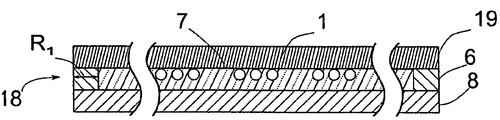
도 2에 도시된 제 2 공정 단계에서, 안정화를 위해 제 1 면(3)을 갖는 제품 웨이퍼(1)가 제 1 캐리어 웨이퍼(8)로 임시로 접합되고, 제 1 중간 층(18)이 접합을 위해 사용된다. 본원에 도시된 실시예에서, 제 1 중간 층(18)은 제 1 접착 층(6)과 제 1 필름(7)을 포함하고, 제 1 접착 층(6)이 접합을 위해 사용되고, 필름(7)이 범프(4)의 매립(embedding)을 위해 사용된다. 도 1 내지 12는, 예시적 실시예에서의 하나의 단면을 도시하며, 여기서, 제품 웨이퍼(1)는 300밀리미터의 지름(D)을 갖는 둥근 디스크(disk)로 만들어진다. 그러나 제품 웨이퍼(1)는 그 밖의 다른 임의의 디스크 형태 및 상이한 지름(D)을 가질 수 있다. The
도 2에 도시된 실시예에서, 제 1 접착 층(6)은, 외측 웨이퍼 둘레(19) 영역에 위치하고, 웨이퍼 둘레(19)로부터 지름(D)의 분할 값(fraction) 만큼, 구체적으로, 10분의 1 미만의 링 폭(R1) 만큼 뻗어 있어서, 도시된 실시예에서, 제 1 접착 층(6)에 대한 환형체(annular body)가 나타난다. 비 R1/D는 구체적으로 1/20 미만이고, 바람직하게는 1/30 미만이며, 더 바람직하게는 1/60 미만이고, 더 더욱 바람직하게는 1/120 미만이다. 링의 폭(R1)은 구체적으로 15㎜ 미만이고, 바람직하게는 10㎜ 미만이며, 더 바람직하게는 5㎜ 미만이고, 더 더욱 바람직하게는 2㎜ 미만이다. 필름(7)이 환형체 내에 있고, 필름이, 제품 웨이퍼(1), 제 1 접착 층(6) 및 제 1 캐리어 웨이퍼(8)에 의해 완전히 둘러싸인다.2, the first
하나의 바람직한 실시예에 따르는 필름(7)이, 제 1 접착 층(6)의 부분 코팅으로서 제공되며, 이 대안적 실시예에서, 접착 층(6)은 제 1 캐리어 웨이퍼(8) 전체에 걸쳐 뻗어 있다. 도 2에 도시된 필름(7)과 유사한 크기로 부분 코팅이 제공된다. A
도 11에 도시된 대안적 실시예의 경우, 제 1 중간 층(18')이 단일 물질로부터 형성되고, 제품 웨이퍼(1)의 전체 영역에 걸쳐 뻗어 있다. 이 경우, 제 1 중간 층(18')의 접착력(adhesion capacity)은 온도에 따라 달라져서, 온도가 높아질수록, 특히 점성의 감소 때문에, 접착력, 따라서, 접합력(bonding force)이 감소하고, 시멘트(cement)가 전단력에 대한 저항을 감소시켰다. 11, a first intermediate layer 18 'is formed from a single material and extends over the entire area of the
도 3에 도시된 본 발명에 따르는 제 1 공정 단계에서, 공지된 방법에 의해, 제품 웨이퍼(1)는, 도 1에 도시된 본래의 두께(H1)에서부터, 도 10에 도시된 최종 제품에 대응하는 150㎛ 미만, 구체적으로 100㎛ 미만, 바람직하게는 70㎛ 미만, 더 바람직하게는 50㎛ 미만, 더 더욱 바람직하게는 30㎛ 미만, 더 더욱 바람직하게는 20㎛ 미만의 두께(H2)까지로, 백-씨닝 가공된다.In a first process step according to the invention shown in Fig. 3, by means of a known process, the
도 4에 도시된 네 번째 방법 단계에서, 제품 웨이퍼(1)를 관통하는 비아(VIA)(9)가 제품 웨이퍼(1) 내부로 에칭-형성되어, 범프(4)들 사이에서 제 1 면(3)에서 제 2 면(2)으로의 전기 연결이 형성될 수 있고, 도 5에 도시된 다섯 번째 방법 단계에서, 제 2 면(2)으로 도포될 범프(10) 또는 범프 그룹(11)이 형성될 수 있다. 4, a via (VIA) 9 penetrating the
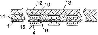
도 6에 도시된 여섯 번째 단계에서, 칩(12)이 적절한 범프(10) 또는 범프 그룹(11)으로 제공된다.In the sixth step shown in Fig. 6, the
본 발명에 따르는 방법 단계들 중 하나가 도 7에 도시된 일곱 번째 방법 단계이며, 여기서, 도 2에 도시된 방법 단계와 유사한 방식으로, 제 2 면(2)이, 제 1 중간 층(18)과 상이한 하나 이상의 관련 속성을 갖는 제 2 중간 층(17)을 통해, 제 2 캐리어 웨이퍼(13)로 접합된다.One of the method steps according to the present invention is the seventh method step shown in Fig. 7, wherein the
이 실시예에서, 제 2 중간 층(17)은, 마찬가지로, 제품 웨이퍼(1)의 외측 웨이퍼 둘레(19)로부터 지름(D)의 분할 값만큼, 구체적으로 링 폭(R2)(최대, 지름(D)의 10분의 1)만큼 뻗어 있는 제 2 접착 층(14)으로 구성된다. 이 실시예에서, 제 2 접착 층(14)은 링 폭(R2)을 갖는 환형 링으로 만들어지며, 여기서 링 폭(R2)은 제 1 접착 층(6)의 링 폭(R1)보다 크다. 비 R1/R2는 1/10 내지 9/10이며, 특히, 1/5 내지 4/5이고, 바람직하게는 1/4 내지 3/4이며, 더 바람직하게는 1/3 내지 2/3이다. 비 R2/D는 구체적으로 1/20 미만이며, 바람직하게는 1/30 미만이고, 더 바람직하게는 1/60 미만이며, 더 더욱 바람직하게는 1/120이다. 링 폭(R2)은 구체적으로 15㎜ 미만이며, 바람직하게는 10㎜ 미만이고, 더 바람직하게는 5㎜이며, 더 더욱 바람직하게는 2㎜ 미만이다. In this embodiment, the second
이러한 방식으로, 제품 웨이퍼(1)와 제 2 캐리어 웨이퍼(13) 사이의 제 2 접착 층(14)에 대한 유효 접착 영역/접합 영역이 더 넓어진다.In this way, the effective bonding area / bonding area for the second
이 실시예와 조합될 수 있는 본 발명의 하나의 대안적 실시예에서, 제 1 중간 층(18)의 두께(B1)가 제 2 중간 층(17)의 두께(B2)보다 크며, 특히, 비 B1/B2는 적어도 3/2이고, 바람직하게는 2/1이며, 더 바람직하게는 3/1이며, 이상적으로는 적어도 4/1이다.In one alternative embodiment of the invention, which can be combined with the embodiment, the first thickness (B 1) of the
도 8에 도시된 방법 단계에서, 제 1 접착 층(6)의 접합력을 감소시키고, 제품 웨이퍼(2)로부터 멀어지는 방향의 장력을 적용함으로써, 제 1 캐리어 웨이퍼(8)가 분리된다. 접합력의 감소는 이전 방법 단계에서 이미 구현되거나, 수행됐을 수 있다. 또는, 제품 웨이퍼(1)에 평행하게 제 1 및 제 2 캐리어 웨이퍼(8, 13)에 전단력을 반대 방향으로 작용시킴으로써, 제 2 캐리어 웨이퍼(8)가 잘라내질 수 있다. 또 다른 대안예가, 캐리어 웨이퍼를, 캐리어 웨이퍼의 변부에서부터 박리(peel off)하는 것을 포함한다. 박리 중에, 캐리어 웨이퍼는 자신의 변부에서, 탄성적으로 휘어지고, 그 결과로, 제 2 캐리어 웨이퍼와 제품 웨이퍼의 휘어짐을 상쇄하기 위해, 제 2 캐리어 웨이퍼와 제품 웨이퍼가 지지대에 고정되어 있는 동안, 캐리어 웨이퍼의 변부에서부터 시작하여, 중심 쪽으로, 그리고 반대편 변부까지로, 분리 전선(separating front)이 전파된다. 한 가지 바람직한 실시예에서, 기계적 분리에 의해, 특히, 중간 층의 둘레 변부 상의 하나의 지점(site)에 기계적 요소를 도입함으로써, 분리가 이뤄질 수 있다. 예를 들어, 기계적 요소는 평판형 쐐기일 수 있다. 8, the
제 1 접착 층(6)에 비해 제 2 접착 층(14)의 접착 영역이 더 넓고, 접합력이 더 강함으로써, 제 1 캐리어 웨이퍼(8)가 자동으로 분리된다. 분리 동안, 필름(7)과 접착 층(6)의 잔여물이 제품 웨이퍼(2) 상에 남아 있는 경우, 상기 잔여물은 세정 단계에 의해 제거될 수 있다. 도 7 및 8에 도시된 실시예에서, 제 1 캐리어 웨이퍼(8)가 기하학적 구성을 기초로, 즉, 제 2 접착 층(14)의 더 커진 접착 영역 때문에 분리된다. 도 11에 도시된 대안적 실시예에서, 제 1 중간 층(18')이 자신의 접착력 또는 접합력을, 제 2 중간 층(17')보다 더 빨리 감소시키도록, 제 1 중간 층(18')은 제 2 중간 층(17')과 다른 열물성을 가진다.The bonding area of the second
본 발명의 하나의 바람직한 실시예에 따르면, 방법은 다음과 같이 진행된다:According to one preferred embodiment of the present invention, the method proceeds as follows:
- 제품 웨이퍼(1)의 제 1 면(3)을, 적어도 변부 측에 도포되는 하나의 제 1 접착 층으로 구성되는 제 1 중간 층(18)을 갖는 제 1 강성 캐리어 웨이퍼(8) 상에 접합하기,The
- 제 1 접착 층(6)을 적어도 부분적으로 용해하기,- at least partially dissolving the first adhesive layer (6)
- 제품 웨이퍼(1)의 제 2 면(2)을, 적어도 변부 측에 도포되는 제 2 접착 층(14)으로 구성되는 제 2 중간 층(17)을 갖는 제 2 강성 캐리어 웨이퍼(13) 상에 접합하기,The
- 특히, 제품 웨이퍼(1)에 평행하게 제 1 캐리어 웨이퍼(8)와 제 2 캐리어 웨이퍼(13)로 반대방향으로 전단력을 적용하거나, 제 1 캐리어 웨이퍼(8)를 박리함으로써, 제 1 캐리어 웨이퍼를 분리하기.In particular, by applying a shear force in the opposite direction to the
제 1 및 제 2 접착 층(6, 14)은 동일한 물질이며, 각각의 캐리어 웨이퍼의 전체 영역에 걸쳐 분포되어 있으며, 캐리어 웨이퍼의 제 1 및 제 2 접착 층(6, 14)의 제 1 및 제 2 부분 코팅으로의 접착 층의 각각의 접합 영역/접착 영역에 제공되어, 도포의 영역에서의 접착력의 개별적인 감소가 이뤄질 수 있다.The first and second
도 12에 도시된 대안적 실시예에서, 제 1 접착 층(18")이 도 7에 도시된 실시예와 유사하게 만들어지며, 이때, 링 폭(R1')은 제 2 접착 층(17")의 링 폭(R2')보다 더 작아서, 두 접착 층(17", 18")이 서로 동일한 물질인 경우, 광원(29)이 제 1 접착 층(18")과 제 2 접착 층(17")에 작용하도록 할 수 있다. 제 2 접착 층(17")의 더 넓은 링 폭(R2')으로 인해, 특히, 광원(29)이 비교적 집중된 방식으로 작용하도록 만들어지기 때문에, 제 2 캐리어 웨이퍼(13)보다 먼저, 제 1 캐리어 웨이퍼(8)가 분리될 수 있다. 예를 들어 광원은 UV 광원일 수 있다. 12, a first
또는 제 1 접착 층(18")과 제 2 접착 층(17")이 서로 다른 광 강도/광 주파수에 대해 반응하도록 만들어질 수 있다.Or the first
앞서 기재된 실시예들의 공통점은, 대응하는 동작에 대해, 제품 웨이퍼(1)와 제 1 캐리어 웨이퍼(8) 간의 접착력 또는 접합력이, 제품 웨이퍼(1)와 제 2 캐리어 웨이퍼(13) 간의 접착력 또는 접합력에 비해 더 작도록, 제 1 접착 층(18, 18', 18")이 제 2 접착 층(17, 17', 17")과 상이하다는 것이다.The common point of the previously described embodiments is that the adhesive force or bonding force between the
도 9에 도시된 아홉 번째 방법 단계에서, 칩(15)이 범프(4)에 제공되고, 따라서, 도 6에서 도시된 여섯 번째 방법 단계와 유사하게 전도성 방식으로 칩(12)으로 전기 연결된다.In the ninth method step shown in Fig. 9, a
도 10에서 도시된 열 번째 단계에서의 제 2 캐리어 웨이퍼(13)의 분리 후, 두 면에 장착되는 제품 웨이퍼(16)가 유지된다. 제품 웨이퍼(16)의 스택(stack)이 생산될 경우, 도 9에 도시된 아홉 번째 방법 단계에 따라, 칩(12, 15)이 장착된 거의 임의의 개수의 제품 웨이퍼(1)가 적층될 수 있고, N번째 접착 층은, 분리 동안, N+1번째 접착 층보다 더 작은 접합력을 가져야 한다. 이는, 앞서 기재된 절차와 유사하게, N번째 접착 층/중간 층의 수정이, N번째 캐리어 웨이퍼가 분리될 때 바로 발생하거나, N번째 캐리어 웨이퍼의 분리 전에, 특히, N+1번째 캐리어 웨이퍼의 접합 전에 발생한다.After the separation of the
필름(7)을 대신하여, 필름(7)이 차지하는 영역이 기체로 채워지거나, 배기될 수 있다. Instead of the
도 1 내지 9에서 도시된 실시예에서, 제 1 및 제 2 접착 층(6, 14)의 용해 가 화학적 용매에 의해 보조되는 것이 바람직하다. 따라서 접착 층을 용해하기 위한 화학적, 열적, 광학적, 및 기계적 방법 단계들의 조합이 가능하다. In the embodiment shown in Figs. 1-9, it is preferred that the dissolution of the first and second
블랭킷(blanket) 중간 층을 이용하는 방법(예를 들어, 도 11에 도시된 방법)에서, 광학적 및/또는 열적 용해 방법이 추천되며, 용매의 사용은 확산 시간 때문에 웨이퍼 둘레(19)에서는 덜 적합하다.In the method of using a blanket intermediate layer (e.g., the method shown in Figure 11), optical and / or thermal dissolution methods are recommended and the use of solvent is less suitable for
1 제품 웨이퍼
2 제 2 면
3 제 1 면
4 범프
5 범프 그룹
6 제 1 접착 층
7 필름
8 제 1 캐리어 웨이퍼
9 비아
10 범프
11 범프 그룹
12 칩
13 제 2 캐리어 웨이퍼
14 제 2 접착 층
15 칩
16 양면 장착 제품 웨이퍼
17, 17', 17" 제 2 중간 층
18, 18', 18" 제 1 중간 층
19 웨이퍼 둘레
29 광원
D 지름
H1 웨이퍼 두께
H2 웨이퍼 두께
R1, R1' 링 폭
R2, R2' 링 폭
B1 중간 층의 두께
B2 중간 층의 두께1 product wafer
2 The second side
3 First Side
4 bump
5 Bump Group
6 First adhesive layer
7 film
8 First carrier wafer
9 Via
10 bump
11 Bump Group
12 chips
13 second carrier wafer
14 Second adhesive layer
15 chips
16 Double-sided mounting product wafer
17, 17 ', 17 " second intermediate layer
18, 18 ', 18 " first intermediate layer
19 Wafer circumference
29 light source
D diameter
H 1 wafer thickness
H 2 wafer thickness
R 1 , R 1 'ring width
R 2 , R 2 'ring width
B 1 Thickness of the intermediate layer
B 2 Thickness of the intermediate layer
Claims (16)
제품 웨이퍼의 제 1 면을, 제 1 중간 층을 포함하는 제 1 강성 캐리어 웨이퍼에 일시적으로 접합하는 단계 - 상기 제 1 중간 층은 제품 웨이퍼의 제 1 면의 적어도 변부(edge side)에 도포되는 하나의 제 1 접착 층을 포함하고, 상기 제 1 접착 층은 제 1 물질로 제조됨 - 와,
상기 제 1 면의 반대편에 있는 제품 웨이퍼의 제 2 면에 칩의 제공에 의해 상기 제 2 면을 가공하는 단계와,
제품 웨이퍼의 제 2 면을, 제 2 중간 층을 포함하는 제 2 강성 캐리어 웨이퍼에 접합하는 단계 - 상기 제 2 중간 층은 제품 웨이퍼의 제 2 면의 적어도 변부에 도포되는 하나의 제 2 접착 층을 포함하고, 상기 제 2 접착 층은 제 2 물질로 제조되며, 제 1 접착 층과 제 2 접착 층은 상이한 물질로 제조되어서, 제품 웨이퍼에 접합되는 두 강성 캐리어 웨이퍼 모두 제품 웨이퍼로부터 선택적으로 분리될 수 있음 - 와,
제 1 강성 캐리어 웨이퍼 및 제 2 강성 캐리어 웨이퍼 모두가 제품 웨이퍼에 접합한 후에, 제 1 강성 캐리어 웨이퍼, 제 2 강성 캐리어 웨이퍼 및 제품 웨이퍼의 조합물에 제 1 힘을 가하는 단계 - 제 1 강성 캐리어 웨이퍼 및 제 1 중간 층은 제품 웨이퍼로부터 분리됨 - 와,
제 1 강성 캐리어 웨이퍼 및 제 1 중간 층이 제품 웨이퍼로부터 분리된 후에, 제 2 강성 캐리어 웨이퍼에 제 2 힘을 가하는 단계 - 제 2 강성 캐리어 웨이퍼 및 제 2 중간 층은 제품 웨이퍼로부터 분리됨 - 를 포함하되, 상기 제 1 접착 층 및 상기 제 2 접착 층은 열가소성 시멘트로 제조된 것을 특징으로 하는 제품 웨이퍼를 제작하기 위한 방법.CLAIMS 1. A method for fabricating a product wafer on both sides of which a chip is provided,
Temporarily bonding a first side of a product wafer to a first rigid carrier wafer comprising a first intermediate layer, the first intermediate layer having a first side coated with a first side coated on at least the edge side of the first side of the product wafer The first adhesive layer being made of a first material,
Machining the second surface by providing a chip on a second surface of the product wafer opposite the first surface;
Bonding a second side of the product wafer to a second rigid carrier wafer comprising a second intermediate layer, wherein the second intermediate layer comprises one second adhesive layer applied to at least the sides of the second side of the product wafer Wherein the first adhesive layer and the second adhesive layer are made of different materials so that both rigid carrier wafers bonded to the product wafer can be selectively removed from the product wafer Yes - and,
Applying a first force to a combination of a first rigid carrier wafer, a second rigid carrier wafer, and a product wafer after both the first rigid carrier wafer and the second rigid carrier wafer are bonded to the product wafer, And a first intermediate layer separated from the product wafer,
Applying a second force to the second rigid carrier wafer after the first rigid carrier wafer and the first intermediate layer are separated from the product wafer, wherein the second rigid carrier wafer and the second intermediate layer are separated from the product wafer, Wherein the first adhesive layer and the second adhesive layer are made of thermoplastic cement.
제품 웨이퍼의 제 1 면을, 제 1 중간 층을 포함하는 제 1 강성 캐리어 웨이퍼에 일시적으로 접합하는 단계 - 상기 제 1 중간 층은 제품 웨이퍼의 제 1 면의 적어도 변부(edge side)에 도포되는 하나의 제 1 접착 층을 포함하고, 상기 제 1 접착 층은 제 1 물질로 제조됨 - 와,
상기 제 1 면의 반대편에 있는 제품 웨이퍼의 제 2 면에 칩의 제공에 의해 상기 제 2 면을 가공하는 단계와,
제품 웨이퍼의 제 2 면을, 제 2 중간 층을 포함하는 제 2 강성 캐리어 웨이퍼에 접합하는 단계 - 상기 제 2 중간 층은 제품 웨이퍼의 제 2 면의 적어도 변부에 도포되는 하나의 제 2 접착 층을 포함하고, 상기 제 2 접착 층은 제 2 물질로 제조되며, 제 1 접착 층의 제품 웨이퍼 또는 제 1 강성 캐리어 웨이퍼와의 접촉 영역은, 제 2 접착 층의 제품 웨이퍼 또는 제 2 강성 캐리어 웨이퍼와의 접촉 영역보다 작아서, 제품 웨이퍼에 접합되는 두 강성 캐리어 웨이퍼 모두 제품 웨이퍼로부터 선택적으로 분리될 수 있음 - 와,
제 1 강성 캐리어 웨이퍼 및 제 2 강성 캐리어 웨이퍼 모두가 제품 웨이퍼에 접합한 후에, 제 1 강성 캐리어 웨이퍼, 제 2 강성 캐리어 웨이퍼 및 제품 웨이퍼의 조합물에 제 1 힘을 가하는 단계 - 제 1 강성 캐리어 웨이퍼 및 제 1 중간 층은 제품 웨이퍼로부터 분리됨 - 와,
제 1 강성 캐리어 웨이퍼 및 제 1 중간 층이 제품 웨이퍼로부터 분리된 후에, 제 2 강성 캐리어 웨이퍼에 제 2 힘을 가하는 단계 - 제 2 강성 캐리어 웨이퍼 및 제 2 중간 층은 제품 웨이퍼로부터 분리됨 - 를 포함하되, 상기 제 1 접착 층 및 상기 제 2 접착 층은 열가소성 시멘트로 제조된 것을 특징으로 하는 제품 웨이퍼를 제작하기 위한 방법.CLAIMS 1. A method for fabricating a product wafer on both sides of which a chip is provided,
Temporarily bonding a first side of a product wafer to a first rigid carrier wafer comprising a first intermediate layer, the first intermediate layer having a first side coated with a first side coated on at least the edge side of the first side of the product wafer The first adhesive layer being made of a first material,
Machining the second surface by providing a chip on a second surface of the product wafer opposite the first surface;
Bonding a second side of the product wafer to a second rigid carrier wafer comprising a second intermediate layer, wherein the second intermediate layer comprises one second adhesive layer applied to at least the sides of the second side of the product wafer Wherein the second adhesive layer is made of a second material and the area of contact of the first adhesive layer with the product wafer or the first rigid carrier wafer is such that the area of contact with the product wafer of the second adhesive layer or with the second rigid carrier wafer Both of the two rigid carrier wafers that are smaller than the contact area and are bonded to the product wafer can be selectively removed from the product wafer,
Applying a first force to a combination of a first rigid carrier wafer, a second rigid carrier wafer, and a product wafer after both the first rigid carrier wafer and the second rigid carrier wafer are bonded to the product wafer, And a first intermediate layer separated from the product wafer,
Applying a second force to the second rigid carrier wafer after the first rigid carrier wafer and the first intermediate layer are separated from the product wafer, wherein the second rigid carrier wafer and the second intermediate layer are separated from the product wafer, Wherein the first adhesive layer and the second adhesive layer are made of thermoplastic cement.
제품 웨이퍼의 제 1 면을, 제 1 중간 층을 포함하는 제 1 강성 캐리어 웨이퍼에 일시적으로 접합하는 단계 - 상기 제 1 중간 층은 제품 웨이퍼의 제 1 면의 적어도 변부(edge side)에 도포되는 하나의 제 1 접착 층을 포함하고, 상기 제 1 접착 층은 제 1 물질로 제조됨 - 와,
상기 제 1 면의 반대편에 있는 제품 웨이퍼의 제 2 면에 칩의 제공에 의해 상기 제 2 면을 가공하는 단계와,
제품 웨이퍼의 제 2 면을, 제 2 중간 층을 포함하는 제 2 강성 캐리어 웨이퍼에 접합하는 단계 - 상기 제 2 중간 층은 제품 웨이퍼의 제 2 면의 적어도 변부에 도포되는 하나의 제 2 접착 층을 포함하고, 상기 제 2 접착 층은 제 2 물질로 제조되며, 제 1 접착 층의 두께는 제 2 접착 층의 두께보다 얇아서, 제품 웨이퍼에 접합되는 두 강성 캐리어 웨이퍼 모두 제품 웨이퍼로부터 선택적으로 분리될 수 있음 - 와,
제 1 강성 캐리어 웨이퍼 및 제 2 강성 캐리어 웨이퍼 모두가 제품 웨이퍼에 접합한 후에, 제 1 강성 캐리어 웨이퍼, 제 2 강성 캐리어 웨이퍼 및 제품 웨이퍼의 조합물에 제 1 힘을 가하는 단계 - 제 1 강성 캐리어 웨이퍼 및 제 1 중간 층은 제품 웨이퍼로부터 분리됨 - 와,
제 1 강성 캐리어 웨이퍼 및 제 1 중간 층이 제품 웨이퍼로부터 분리된 후에, 제 2 강성 캐리어 웨이퍼에 제 2 힘을 가하는 단계 - 제 2 강성 캐리어 웨이퍼 및 제 2 중간 층은 제품 웨이퍼로부터 분리됨 - 를 포함하되, 상기 제 1 접착 층 및 상기 제 2 접착 층은 열가소성 시멘트로 제조된 것을 특징으로 하는 제품 웨이퍼를 제작하기 위한 방법.CLAIMS 1. A method for fabricating a product wafer on both sides of which a chip is provided,
Temporarily bonding a first side of a product wafer to a first rigid carrier wafer comprising a first intermediate layer, the first intermediate layer having a first side coated with a first side coated on at least the edge side of the first side of the product wafer The first adhesive layer being made of a first material,
Machining the second surface by providing a chip on a second surface of the product wafer opposite the first surface;
Bonding a second side of the product wafer to a second rigid carrier wafer comprising a second intermediate layer, wherein the second intermediate layer comprises one second adhesive layer applied to at least the sides of the second side of the product wafer Wherein the second adhesive layer is made of a second material and wherein the thickness of the first adhesive layer is thinner than the thickness of the second adhesive layer so that both rigid carrier wafers bonded to the product wafer can be selectively detached from the product wafer Yes - and,
Applying a first force to a combination of a first rigid carrier wafer, a second rigid carrier wafer, and a product wafer after both the first rigid carrier wafer and the second rigid carrier wafer are bonded to the product wafer, And a first intermediate layer separated from the product wafer,
Applying a second force to the second rigid carrier wafer after the first rigid carrier wafer and the first intermediate layer are separated from the product wafer, wherein the second rigid carrier wafer and the second intermediate layer are separated from the product wafer, Wherein the first adhesive layer and the second adhesive layer are made of thermoplastic cement.
Applications Claiming Priority (1)
| Application Number | Priority Date | Filing Date | Title |
|---|---|---|---|
| PCT/EP2010/002055 WO2011120537A1 (en) | 2010-03-31 | 2010-03-31 | Method for producing a wafer equipped with chips on two sides |
Related Parent Applications (1)
| Application Number | Title | Priority Date | Filing Date |
|---|---|---|---|
| KR1020167016168A Division KR20160075845A (en) | 2010-03-31 | 2010-03-31 | Method for producing a wafer equipped with chips on two sides |
Publications (2)
| Publication Number | Publication Date |
|---|---|
| KR20170042817A KR20170042817A (en) | 2017-04-19 |
| KR101856429B1 true KR101856429B1 (en) | 2018-05-09 |
Family
ID=42286741
Family Applications (3)
| Application Number | Title | Priority Date | Filing Date |
|---|---|---|---|
| KR1020177009655A Active KR101856429B1 (en) | 2010-03-31 | 2010-03-31 | Method for producing a wafer equipped with chips on two sides |
| KR1020167016168A Ceased KR20160075845A (en) | 2010-03-31 | 2010-03-31 | Method for producing a wafer equipped with chips on two sides |
| KR1020127023406A Ceased KR20130040779A (en) | 2010-03-31 | 2010-03-31 | Method for producing a wafer equipped with chips on two sides |
Family Applications After (2)
| Application Number | Title | Priority Date | Filing Date |
|---|---|---|---|
| KR1020167016168A Ceased KR20160075845A (en) | 2010-03-31 | 2010-03-31 | Method for producing a wafer equipped with chips on two sides |
| KR1020127023406A Ceased KR20130040779A (en) | 2010-03-31 | 2010-03-31 | Method for producing a wafer equipped with chips on two sides |
Country Status (8)
| Country | Link |
|---|---|
| US (1) | US9224630B2 (en) |
| EP (1) | EP2553719B1 (en) |
| JP (1) | JP5763169B2 (en) |
| KR (3) | KR101856429B1 (en) |
| CN (1) | CN102812546B (en) |
| SG (1) | SG183820A1 (en) |
| TW (1) | TWI518758B (en) |
| WO (1) | WO2011120537A1 (en) |
Families Citing this family (7)
| Publication number | Priority date | Publication date | Assignee | Title |
|---|---|---|---|---|
| WO2013006865A2 (en) | 2011-07-07 | 2013-01-10 | Brewer Science Inc. | Methods of transferring device wafers or layers between carrier substrates and other surfaces |
| AU2015244410A1 (en) * | 2014-04-09 | 2016-11-10 | Lionel O. Barthold | Multi-module dc-to-dc power transformation system |
| WO2020178080A1 (en) * | 2019-03-05 | 2020-09-10 | Evatec Ag | Method for processing fragile substrates employing temporary bonding of the substrates to carriers |
| US12103787B2 (en) | 2020-02-18 | 2024-10-01 | Ev Group E. Thallner Gmbh | Method and device for transferring components |
| US20250153481A1 (en) | 2022-03-25 | 2025-05-15 | Ev Group E. Thallner Gmbh | Method and substrate system for the separation of carrier substrates |
| KR102788502B1 (en) * | 2023-07-27 | 2025-04-01 | 한국기계연구원 | Wafer module capable of being debonded effectively, and method for bonding and debonding the same |
| WO2025228530A1 (en) | 2024-05-02 | 2025-11-06 | Ev Group E. Thallner Gmbh | Method for temporarily connecting a product substrate and a carrier substrate, carrier substrate, product substrate and layer system and arrangement thereof, and a device for carrying out such a method |
Citations (4)
| Publication number | Priority date | Publication date | Assignee | Title |
|---|---|---|---|---|
| US20050029224A1 (en) * | 2001-04-13 | 2005-02-10 | Bernard Aspar | Detachable substrate or detachable structure and method for the production thereof |
| US20080003780A1 (en) * | 2006-06-30 | 2008-01-03 | Haixiao Sun | Detachable stiffener for ultra-thin die |
| JP2009043962A (en) * | 2007-08-09 | 2009-02-26 | Sony Corp | Manufacturing method of semiconductor device |
| US20090218560A1 (en) * | 2008-01-24 | 2009-09-03 | Brewer Science Inc. | Method for reversibly mounting a device wafer to a carrier substrate |
Family Cites Families (35)
| Publication number | Priority date | Publication date | Assignee | Title |
|---|---|---|---|---|
| JPS6198784A (en) * | 1984-10-20 | 1986-05-17 | Kimurashin Kk | Rolled or laminated double-sided adhesive tape |
| JPH04283283A (en) | 1991-03-08 | 1992-10-08 | Nippon Synthetic Chem Ind Co Ltd:The | Tearable tape |
| JP3686454B2 (en) | 1995-05-10 | 2005-08-24 | 日東電工株式会社 | Adhesive sheet for single use warmer and its warmer |
| WO1997039481A1 (en) * | 1996-04-12 | 1997-10-23 | Northeastern University | An integrated complex-transition metal oxide device and a method of fabricating such a device |
| JPH11105924A (en) | 1997-10-06 | 1999-04-20 | Nitto Denko Corp | Electronic component transport tape |
| JPH11238375A (en) * | 1998-02-20 | 1999-08-31 | Sony Corp | Radiator and disk drive for electronic equipment |
| JP2000326995A (en) | 1999-05-17 | 2000-11-28 | Ogawa Sangyo Kk | Sterilization bag |
| JP2002097041A (en) | 2000-07-17 | 2002-04-02 | Sekisui Chem Co Ltd | Interlayer for laminated glass and laminated glass |
| JP3861669B2 (en) * | 2001-11-22 | 2006-12-20 | ソニー株式会社 | Manufacturing method of multichip circuit module |
| JP2003218063A (en) * | 2002-01-24 | 2003-07-31 | Canon Inc | Adhesive sheet for attaching wafer and processing method using the sheet |
| US6794273B2 (en) | 2002-05-24 | 2004-09-21 | Fujitsu Limited | Semiconductor device and manufacturing method thereof |
| JP4565804B2 (en) | 2002-06-03 | 2010-10-20 | スリーエム イノベイティブ プロパティズ カンパニー | Laminate including ground substrate, method for producing the same, method for producing ultrathin substrate using laminate, and apparatus therefor |
| JP4364535B2 (en) | 2003-03-27 | 2009-11-18 | シャープ株式会社 | Manufacturing method of semiconductor device |
| JP4405246B2 (en) | 2003-11-27 | 2010-01-27 | スリーエム イノベイティブ プロパティズ カンパニー | Manufacturing method of semiconductor chip |
| US7232740B1 (en) * | 2005-05-16 | 2007-06-19 | The United States Of America As Represented By The National Security Agency | Method for bumping a thin wafer |
| US8592286B2 (en) * | 2005-10-05 | 2013-11-26 | Stats Chippac Ltd. | Ultra-thin wafer system and method of manufacture thereof |
| DE102006000687B4 (en) | 2006-01-03 | 2010-09-09 | Thallner, Erich, Dipl.-Ing. | Combination of a carrier and a wafer, device for separating the combination and methods for handling a carrier and a wafer |
| US20080044984A1 (en) * | 2006-08-16 | 2008-02-21 | Taiwan Semiconductor Manufacturing Co., Ltd. | Methods of avoiding wafer breakage during manufacture of backside illuminated image sensors |
| US7838391B2 (en) * | 2007-05-07 | 2010-11-23 | Stats Chippac, Ltd. | Ultra thin bumped wafer with under-film |
| EP2104138A1 (en) | 2008-03-18 | 2009-09-23 | EV Group E. Thallner GmbH | Method for bonding chips onto a wafer |
| JP4572243B2 (en) * | 2008-03-27 | 2010-11-04 | 信越化学工業株式会社 | Thermally conductive laminate and method for producing the same |
| JP2010010644A (en) * | 2008-05-27 | 2010-01-14 | Toshiba Corp | Method of manufacturing semiconductor device |
| JP2010092931A (en) * | 2008-10-03 | 2010-04-22 | Toshiba Corp | Method and apparatus for manufacturing semiconductor device |
| KR20120027237A (en) | 2009-04-16 | 2012-03-21 | 수스 마이크로텍 리소그라피 게엠바하 | Improved apparatus for temporary wafer bonding and debonding |
| US8689437B2 (en) * | 2009-06-24 | 2014-04-08 | International Business Machines Corporation | Method for forming integrated circuit assembly |
| EP2299486B1 (en) * | 2009-09-18 | 2015-02-18 | EV Group E. Thallner GmbH | Method for bonding chips to wafers |
| US8008121B2 (en) * | 2009-11-04 | 2011-08-30 | Stats Chippac, Ltd. | Semiconductor package and method of mounting semiconductor die to opposite sides of TSV substrate |
| US9136144B2 (en) * | 2009-11-13 | 2015-09-15 | Stats Chippac, Ltd. | Method of forming protective material between semiconductor die stacked on semiconductor wafer to reduce defects during singulation |
| US8017439B2 (en) | 2010-01-26 | 2011-09-13 | Texas Instruments Incorporated | Dual carrier for joining IC die or wafers to TSV wafers |
| TWI419302B (en) * | 2010-02-11 | 2013-12-11 | 日月光半導體製造股份有限公司 | Packaging process |
| US8252682B2 (en) * | 2010-02-12 | 2012-08-28 | Taiwan Semiconductor Manufacturing Company, Ltd. | Method for thinning a wafer |
| JP4976522B2 (en) * | 2010-04-16 | 2012-07-18 | 日東電工株式会社 | Thermosetting die bond film, dicing die bond film, and semiconductor device manufacturing method |
| US8852391B2 (en) * | 2010-06-21 | 2014-10-07 | Brewer Science Inc. | Method and apparatus for removing a reversibly mounted device wafer from a carrier substrate |
| US8492197B2 (en) * | 2010-08-17 | 2013-07-23 | Stats Chippac, Ltd. | Semiconductor device and method of forming vertically offset conductive pillars over first substrate aligned to vertically offset BOT interconnect sites formed over second substrate |
| JP2012069919A (en) * | 2010-08-25 | 2012-04-05 | Toshiba Corp | Manufacturing method of semiconductor device |
-
2010
- 2010-03-31 CN CN201080065914.6A patent/CN102812546B/en active Active
- 2010-03-31 JP JP2013501635A patent/JP5763169B2/en active Active
- 2010-03-31 KR KR1020177009655A patent/KR101856429B1/en active Active
- 2010-03-31 EP EP10715497.3A patent/EP2553719B1/en active Active
- 2010-03-31 KR KR1020167016168A patent/KR20160075845A/en not_active Ceased
- 2010-03-31 US US13/635,457 patent/US9224630B2/en active Active
- 2010-03-31 SG SG2012063681A patent/SG183820A1/en unknown
- 2010-03-31 KR KR1020127023406A patent/KR20130040779A/en not_active Ceased
- 2010-03-31 WO PCT/EP2010/002055 patent/WO2011120537A1/en not_active Ceased
-
2011
- 2011-02-25 TW TW100106549A patent/TWI518758B/en active
Patent Citations (4)
| Publication number | Priority date | Publication date | Assignee | Title |
|---|---|---|---|---|
| US20050029224A1 (en) * | 2001-04-13 | 2005-02-10 | Bernard Aspar | Detachable substrate or detachable structure and method for the production thereof |
| US20080003780A1 (en) * | 2006-06-30 | 2008-01-03 | Haixiao Sun | Detachable stiffener for ultra-thin die |
| JP2009043962A (en) * | 2007-08-09 | 2009-02-26 | Sony Corp | Manufacturing method of semiconductor device |
| US20090218560A1 (en) * | 2008-01-24 | 2009-09-03 | Brewer Science Inc. | Method for reversibly mounting a device wafer to a carrier substrate |
Also Published As
| Publication number | Publication date |
|---|---|
| US20130011997A1 (en) | 2013-01-10 |
| WO2011120537A1 (en) | 2011-10-06 |
| KR20170042817A (en) | 2017-04-19 |
| JP2013524493A (en) | 2013-06-17 |
| SG183820A1 (en) | 2012-10-30 |
| EP2553719B1 (en) | 2019-12-04 |
| KR20160075845A (en) | 2016-06-29 |
| TW201145370A (en) | 2011-12-16 |
| CN102812546A (en) | 2012-12-05 |
| CN102812546B (en) | 2015-08-26 |
| KR20130040779A (en) | 2013-04-24 |
| JP5763169B2 (en) | 2015-08-12 |
| US9224630B2 (en) | 2015-12-29 |
| EP2553719A1 (en) | 2013-02-06 |
| TWI518758B (en) | 2016-01-21 |
Similar Documents
| Publication | Publication Date | Title |
|---|---|---|
| TWI446420B (en) | Carrier separation method for semiconductor process | |
| CN101764047B (en) | Method of thinning a semiconductor substrate | |
| KR20170042817A (en) | Method for producing a wafer equipped with chips on two sides | |
| US7226812B2 (en) | Wafer support and release in wafer processing | |
| US7462551B2 (en) | Adhesive system for supporting thin silicon wafer | |
| JP4762671B2 (en) | Dicing tape and semiconductor wafer dicing method | |
| US8846499B2 (en) | Composite carrier structure | |
| KR102061369B1 (en) | Method for the temporary connection of a product substrate to a carrier substrate | |
| JP2008521214A (en) | Thinner semiconductor wafers | |
| JP2019514199A (en) | Method and apparatus for bonding two substrates | |
| JP7728241B2 (en) | Sheet for forming protective film, method for manufacturing chip with protective film, and laminate | |
| TW200426907A (en) | Fabrication method of semiconductor device | |
| JP6457223B2 (en) | Substrate separation method and semiconductor manufacturing apparatus | |
| JP2008028325A (en) | Method of manufacturing semiconductor device | |
| JP2018088492A (en) | Fixing method for workpiece, and processing method for workpiece | |
| KR100759687B1 (en) | Method for thinning substrate and method for manufacturing circuit device | |
| TW201921545A (en) | Substrate processing system and substrate processing method | |
| JP2005277103A (en) | Semiconductor wafer, support, method of manufacturing semiconductor wafer, spacer and semiconductor device | |
| CN118737958A (en) | Semiconductor device and method for manufacturing the same | |
| JP2008034644A (en) | Peeling method | |
| JPH05109679A (en) | Manufacture of semiconductor device | |
| TWI509739B (en) | Method for manufacturing semiconductor device | |
| JP2026064484A (en) | Processing method | |
| CN121058079A (en) | Semiconductor device manufacturing method and semiconductor device | |
| CN120858437A (en) | Semiconductor device manufacturing method and dicing tape |
Legal Events
| Date | Code | Title | Description |
|---|---|---|---|
| A107 | Divisional application of patent | ||
| A201 | Request for examination | ||
| PA0104 | Divisional application for international application |
St.27 status event code: A-0-1-A10-A18-div-PA0104 St.27 status event code: A-0-1-A10-A16-div-PA0104 |
|
| PA0201 | Request for examination |
St.27 status event code: A-1-2-D10-D11-exm-PA0201 |
|
| PG1501 | Laying open of application |
St.27 status event code: A-1-1-Q10-Q12-nap-PG1501 |
|
| E902 | Notification of reason for refusal | ||
| PE0902 | Notice of grounds for rejection |
St.27 status event code: A-1-2-D10-D21-exm-PE0902 |
|
| R17-X000 | Change to representative recorded |
St.27 status event code: A-3-3-R10-R17-oth-X000 |
|
| E601 | Decision to refuse application | ||
| PE0601 | Decision on rejection of patent |
St.27 status event code: N-2-6-B10-B15-exm-PE0601 |
|
| T11-X000 | Administrative time limit extension requested |
St.27 status event code: U-3-3-T10-T11-oth-X000 |
|
| T13-X000 | Administrative time limit extension granted |
St.27 status event code: U-3-3-T10-T13-oth-X000 |
|
| T13-X000 | Administrative time limit extension granted |
St.27 status event code: U-3-3-T10-T13-oth-X000 |
|
| AMND | Amendment | ||
| P11-X000 | Amendment of application requested |
St.27 status event code: A-2-2-P10-P11-nap-X000 |
|
| P13-X000 | Application amended |
St.27 status event code: A-2-2-P10-P13-nap-X000 |
|
| PX0901 | Re-examination |
St.27 status event code: A-2-3-E10-E12-rex-PX0901 |
|
| PX0701 | Decision of registration after re-examination |
St.27 status event code: A-3-4-F10-F13-rex-PX0701 |
|
| X701 | Decision to grant (after re-examination) | ||
| GRNT | Written decision to grant | ||
| PR0701 | Registration of establishment |
St.27 status event code: A-2-4-F10-F11-exm-PR0701 |
|
| PR1002 | Payment of registration fee |
St.27 status event code: A-2-2-U10-U12-oth-PR1002 Fee payment year number: 1 |
|
| PG1601 | Publication of registration |
St.27 status event code: A-4-4-Q10-Q13-nap-PG1601 |
|
| PR1001 | Payment of annual fee |
St.27 status event code: A-4-4-U10-U11-oth-PR1001 Fee payment year number: 4 |
|
| PR1001 | Payment of annual fee |
St.27 status event code: A-4-4-U10-U11-oth-PR1001 Fee payment year number: 5 |
|
| PR1001 | Payment of annual fee |
St.27 status event code: A-4-4-U10-U11-oth-PR1001 Fee payment year number: 6 |
|
| PR1001 | Payment of annual fee |
St.27 status event code: A-4-4-U10-U11-oth-PR1001 Fee payment year number: 7 |
|
| PR1001 | Payment of annual fee |
St.27 status event code: A-4-4-U10-U11-oth-PR1001 Fee payment year number: 8 |
|
| P22-X000 | Classification modified |
St.27 status event code: A-4-4-P10-P22-nap-X000 |