JP7585646B2 - 半導体装置および半導体装置の製造方法 - Google Patents
半導体装置および半導体装置の製造方法 Download PDFInfo
- Publication number
- JP7585646B2 JP7585646B2 JP2020131895A JP2020131895A JP7585646B2 JP 7585646 B2 JP7585646 B2 JP 7585646B2 JP 2020131895 A JP2020131895 A JP 2020131895A JP 2020131895 A JP2020131895 A JP 2020131895A JP 7585646 B2 JP7585646 B2 JP 7585646B2
- Authority
- JP
- Japan
- Prior art keywords
- region
- anode region
- anode
- conductivity type
- semiconductor substrate
- Prior art date
- Legal status (The legal status is an assumption and is not a legal conclusion. Google has not performed a legal analysis and makes no representation as to the accuracy of the status listed.)
- Active
Links
Images


Classifications
-
- H—ELECTRICITY
- H01—ELECTRIC ELEMENTS
- H01L—SEMICONDUCTOR DEVICES NOT COVERED BY CLASS H10
- H01L21/00—Processes or apparatus adapted for the manufacture or treatment of semiconductor or solid state devices or of parts thereof
- H01L21/70—Manufacture or treatment of devices consisting of a plurality of solid state components formed in or on a common substrate or of parts thereof; Manufacture of integrated circuit devices or of parts thereof
- H01L21/71—Manufacture of specific parts of devices defined in group H01L21/70
- H01L21/76—Making of isolation regions between components
- H01L21/761—PN junctions
-
- H—ELECTRICITY
- H01—ELECTRIC ELEMENTS
- H01L—SEMICONDUCTOR DEVICES NOT COVERED BY CLASS H10
- H01L21/00—Processes or apparatus adapted for the manufacture or treatment of semiconductor or solid state devices or of parts thereof
- H01L21/02—Manufacture or treatment of semiconductor devices or of parts thereof
- H01L21/02104—Forming layers
- H01L21/02107—Forming insulating materials on a substrate
- H01L21/02225—Forming insulating materials on a substrate characterised by the process for the formation of the insulating layer
- H01L21/02227—Forming insulating materials on a substrate characterised by the process for the formation of the insulating layer formation by a process other than a deposition process
- H01L21/0223—Forming insulating materials on a substrate characterised by the process for the formation of the insulating layer formation by a process other than a deposition process formation by oxidation, e.g. oxidation of the substrate
- H01L21/02233—Forming insulating materials on a substrate characterised by the process for the formation of the insulating layer formation by a process other than a deposition process formation by oxidation, e.g. oxidation of the substrate of the semiconductor substrate or a semiconductor layer
- H01L21/02236—Forming insulating materials on a substrate characterised by the process for the formation of the insulating layer formation by a process other than a deposition process formation by oxidation, e.g. oxidation of the substrate of the semiconductor substrate or a semiconductor layer group IV semiconductor
-
- H—ELECTRICITY
- H01—ELECTRIC ELEMENTS
- H01L—SEMICONDUCTOR DEVICES NOT COVERED BY CLASS H10
- H01L21/00—Processes or apparatus adapted for the manufacture or treatment of semiconductor or solid state devices or of parts thereof
- H01L21/02—Manufacture or treatment of semiconductor devices or of parts thereof
- H01L21/02104—Forming layers
- H01L21/02107—Forming insulating materials on a substrate
- H01L21/02225—Forming insulating materials on a substrate characterised by the process for the formation of the insulating layer
- H01L21/02227—Forming insulating materials on a substrate characterised by the process for the formation of the insulating layer formation by a process other than a deposition process
- H01L21/02255—Forming insulating materials on a substrate characterised by the process for the formation of the insulating layer formation by a process other than a deposition process formation by thermal treatment
-
- H—ELECTRICITY
- H01—ELECTRIC ELEMENTS
- H01L—SEMICONDUCTOR DEVICES NOT COVERED BY CLASS H10
- H01L21/00—Processes or apparatus adapted for the manufacture or treatment of semiconductor or solid state devices or of parts thereof
- H01L21/02—Manufacture or treatment of semiconductor devices or of parts thereof
- H01L21/04—Manufacture or treatment of semiconductor devices or of parts thereof the devices having potential barriers, e.g. a PN junction, depletion layer or carrier concentration layer
- H01L21/18—Manufacture or treatment of semiconductor devices or of parts thereof the devices having potential barriers, e.g. a PN junction, depletion layer or carrier concentration layer the devices having semiconductor bodies comprising elements of Group IV of the Periodic Table or AIIIBV compounds with or without impurities, e.g. doping materials
- H01L21/22—Diffusion of impurity materials, e.g. doping materials, electrode materials, into or out of a semiconductor body, or between semiconductor regions; Interactions between two or more impurities; Redistribution of impurities
- H01L21/221—Diffusion of impurity materials, e.g. doping materials, electrode materials, into or out of a semiconductor body, or between semiconductor regions; Interactions between two or more impurities; Redistribution of impurities of killers
-
- H—ELECTRICITY
- H01—ELECTRIC ELEMENTS
- H01L—SEMICONDUCTOR DEVICES NOT COVERED BY CLASS H10
- H01L21/00—Processes or apparatus adapted for the manufacture or treatment of semiconductor or solid state devices or of parts thereof
- H01L21/02—Manufacture or treatment of semiconductor devices or of parts thereof
- H01L21/04—Manufacture or treatment of semiconductor devices or of parts thereof the devices having potential barriers, e.g. a PN junction, depletion layer or carrier concentration layer
- H01L21/18—Manufacture or treatment of semiconductor devices or of parts thereof the devices having potential barriers, e.g. a PN junction, depletion layer or carrier concentration layer the devices having semiconductor bodies comprising elements of Group IV of the Periodic Table or AIIIBV compounds with or without impurities, e.g. doping materials
- H01L21/22—Diffusion of impurity materials, e.g. doping materials, electrode materials, into or out of a semiconductor body, or between semiconductor regions; Interactions between two or more impurities; Redistribution of impurities
- H01L21/225—Diffusion of impurity materials, e.g. doping materials, electrode materials, into or out of a semiconductor body, or between semiconductor regions; Interactions between two or more impurities; Redistribution of impurities using diffusion into or out of a solid from or into a solid phase, e.g. a doped oxide layer
- H01L21/2251—Diffusion into or out of group IV semiconductors
- H01L21/2252—Diffusion into or out of group IV semiconductors using predeposition of impurities into the semiconductor surface, e.g. from a gaseous phase
- H01L21/2253—Diffusion into or out of group IV semiconductors using predeposition of impurities into the semiconductor surface, e.g. from a gaseous phase by ion implantation
-
- H—ELECTRICITY
- H01—ELECTRIC ELEMENTS
- H01L—SEMICONDUCTOR DEVICES NOT COVERED BY CLASS H10
- H01L21/00—Processes or apparatus adapted for the manufacture or treatment of semiconductor or solid state devices or of parts thereof
- H01L21/02—Manufacture or treatment of semiconductor devices or of parts thereof
- H01L21/04—Manufacture or treatment of semiconductor devices or of parts thereof the devices having potential barriers, e.g. a PN junction, depletion layer or carrier concentration layer
- H01L21/18—Manufacture or treatment of semiconductor devices or of parts thereof the devices having potential barriers, e.g. a PN junction, depletion layer or carrier concentration layer the devices having semiconductor bodies comprising elements of Group IV of the Periodic Table or AIIIBV compounds with or without impurities, e.g. doping materials
- H01L21/26—Bombardment with radiation
- H01L21/263—Bombardment with radiation with high-energy radiation
- H01L21/265—Bombardment with radiation with high-energy radiation producing ion implantation
- H01L21/26506—Bombardment with radiation with high-energy radiation producing ion implantation in group IV semiconductors
- H01L21/26513—Bombardment with radiation with high-energy radiation producing ion implantation in group IV semiconductors of electrically active species
-
- H—ELECTRICITY
- H01—ELECTRIC ELEMENTS
- H01L—SEMICONDUCTOR DEVICES NOT COVERED BY CLASS H10
- H01L21/00—Processes or apparatus adapted for the manufacture or treatment of semiconductor or solid state devices or of parts thereof
- H01L21/02—Manufacture or treatment of semiconductor devices or of parts thereof
- H01L21/04—Manufacture or treatment of semiconductor devices or of parts thereof the devices having potential barriers, e.g. a PN junction, depletion layer or carrier concentration layer
- H01L21/18—Manufacture or treatment of semiconductor devices or of parts thereof the devices having potential barriers, e.g. a PN junction, depletion layer or carrier concentration layer the devices having semiconductor bodies comprising elements of Group IV of the Periodic Table or AIIIBV compounds with or without impurities, e.g. doping materials
- H01L21/26—Bombardment with radiation
- H01L21/263—Bombardment with radiation with high-energy radiation
- H01L21/265—Bombardment with radiation with high-energy radiation producing ion implantation
- H01L21/266—Bombardment with radiation with high-energy radiation producing ion implantation using masks
-
- H—ELECTRICITY
- H01—ELECTRIC ELEMENTS
- H01L—SEMICONDUCTOR DEVICES NOT COVERED BY CLASS H10
- H01L21/00—Processes or apparatus adapted for the manufacture or treatment of semiconductor or solid state devices or of parts thereof
- H01L21/02—Manufacture or treatment of semiconductor devices or of parts thereof
- H01L21/04—Manufacture or treatment of semiconductor devices or of parts thereof the devices having potential barriers, e.g. a PN junction, depletion layer or carrier concentration layer
- H01L21/18—Manufacture or treatment of semiconductor devices or of parts thereof the devices having potential barriers, e.g. a PN junction, depletion layer or carrier concentration layer the devices having semiconductor bodies comprising elements of Group IV of the Periodic Table or AIIIBV compounds with or without impurities, e.g. doping materials
- H01L21/28—Manufacture of electrodes on semiconductor bodies using processes or apparatus not provided for in groups H01L21/20 - H01L21/268
- H01L21/283—Deposition of conductive or insulating materials for electrodes conducting electric current
- H01L21/285—Deposition of conductive or insulating materials for electrodes conducting electric current from a gas or vapour, e.g. condensation
- H01L21/28506—Deposition of conductive or insulating materials for electrodes conducting electric current from a gas or vapour, e.g. condensation of conductive layers
- H01L21/28512—Deposition of conductive or insulating materials for electrodes conducting electric current from a gas or vapour, e.g. condensation of conductive layers on semiconductor bodies comprising elements of Group IV of the Periodic Table
- H01L21/28537—Deposition of Schottky electrodes
-
- H—ELECTRICITY
- H01—ELECTRIC ELEMENTS
- H01L—SEMICONDUCTOR DEVICES NOT COVERED BY CLASS H10
- H01L21/00—Processes or apparatus adapted for the manufacture or treatment of semiconductor or solid state devices or of parts thereof
- H01L21/70—Manufacture or treatment of devices consisting of a plurality of solid state components formed in or on a common substrate or of parts thereof; Manufacture of integrated circuit devices or of parts thereof
- H01L21/77—Manufacture or treatment of devices consisting of a plurality of solid state components or integrated circuits formed in, or on, a common substrate
-
- H—ELECTRICITY
- H10—SEMICONDUCTOR DEVICES; ELECTRIC SOLID-STATE DEVICES NOT OTHERWISE PROVIDED FOR
- H10D—INORGANIC ELECTRIC SEMICONDUCTOR DEVICES
- H10D12/00—Bipolar devices controlled by the field effect, e.g. insulated-gate bipolar transistors [IGBT]
- H10D12/01—Manufacture or treatment
- H10D12/021—Manufacture or treatment of gated diodes, e.g. field-controlled diodes [FCD]
-
- H—ELECTRICITY
- H10—SEMICONDUCTOR DEVICES; ELECTRIC SOLID-STATE DEVICES NOT OTHERWISE PROVIDED FOR
- H10D—INORGANIC ELECTRIC SEMICONDUCTOR DEVICES
- H10D12/00—Bipolar devices controlled by the field effect, e.g. insulated-gate bipolar transistors [IGBT]
- H10D12/211—Gated diodes
-
- H—ELECTRICITY
- H10—SEMICONDUCTOR DEVICES; ELECTRIC SOLID-STATE DEVICES NOT OTHERWISE PROVIDED FOR
- H10D—INORGANIC ELECTRIC SEMICONDUCTOR DEVICES
- H10D12/00—Bipolar devices controlled by the field effect, e.g. insulated-gate bipolar transistors [IGBT]
- H10D12/411—Insulated-gate bipolar transistors [IGBT]
- H10D12/441—Vertical IGBTs
- H10D12/461—Vertical IGBTs having non-planar surfaces, e.g. having trenches, recesses or pillars in the surfaces of the emitter, base or collector regions
- H10D12/481—Vertical IGBTs having non-planar surfaces, e.g. having trenches, recesses or pillars in the surfaces of the emitter, base or collector regions having gate structures on slanted surfaces, on vertical surfaces, or in grooves, e.g. trench gate IGBTs
-
- H—ELECTRICITY
- H10—SEMICONDUCTOR DEVICES; ELECTRIC SOLID-STATE DEVICES NOT OTHERWISE PROVIDED FOR
- H10D—INORGANIC ELECTRIC SEMICONDUCTOR DEVICES
- H10D62/00—Semiconductor bodies, or regions thereof, of devices having potential barriers
- H10D62/10—Shapes, relative sizes or dispositions of the regions of the semiconductor bodies; Shapes of the semiconductor bodies
- H10D62/102—Constructional design considerations for preventing surface leakage or controlling electric field concentration
-
- H—ELECTRICITY
- H10—SEMICONDUCTOR DEVICES; ELECTRIC SOLID-STATE DEVICES NOT OTHERWISE PROVIDED FOR
- H10D—INORGANIC ELECTRIC SEMICONDUCTOR DEVICES
- H10D62/00—Semiconductor bodies, or regions thereof, of devices having potential barriers
- H10D62/10—Shapes, relative sizes or dispositions of the regions of the semiconductor bodies; Shapes of the semiconductor bodies
- H10D62/124—Shapes, relative sizes or dispositions of the regions of semiconductor bodies or of junctions between the regions
- H10D62/126—Top-view geometrical layouts of the regions or the junctions
- H10D62/127—Top-view geometrical layouts of the regions or the junctions of cellular field-effect devices, e.g. multicellular DMOS transistors or IGBTs
-
- H—ELECTRICITY
- H10—SEMICONDUCTOR DEVICES; ELECTRIC SOLID-STATE DEVICES NOT OTHERWISE PROVIDED FOR
- H10D—INORGANIC ELECTRIC SEMICONDUCTOR DEVICES
- H10D62/00—Semiconductor bodies, or regions thereof, of devices having potential barriers
- H10D62/10—Shapes, relative sizes or dispositions of the regions of the semiconductor bodies; Shapes of the semiconductor bodies
- H10D62/129—Cathode regions of diodes
-
- H—ELECTRICITY
- H10—SEMICONDUCTOR DEVICES; ELECTRIC SOLID-STATE DEVICES NOT OTHERWISE PROVIDED FOR
- H10D—INORGANIC ELECTRIC SEMICONDUCTOR DEVICES
- H10D62/00—Semiconductor bodies, or regions thereof, of devices having potential barriers
- H10D62/10—Shapes, relative sizes or dispositions of the regions of the semiconductor bodies; Shapes of the semiconductor bodies
- H10D62/17—Semiconductor regions connected to electrodes not carrying current to be rectified, amplified or switched, e.g. channel regions
- H10D62/393—Body regions of DMOS transistors or IGBTs
-
- H—ELECTRICITY
- H10—SEMICONDUCTOR DEVICES; ELECTRIC SOLID-STATE DEVICES NOT OTHERWISE PROVIDED FOR
- H10D—INORGANIC ELECTRIC SEMICONDUCTOR DEVICES
- H10D62/00—Semiconductor bodies, or regions thereof, of devices having potential barriers
- H10D62/50—Physical imperfections
- H10D62/53—Physical imperfections the imperfections being within the semiconductor body
-
- H—ELECTRICITY
- H10—SEMICONDUCTOR DEVICES; ELECTRIC SOLID-STATE DEVICES NOT OTHERWISE PROVIDED FOR
- H10D—INORGANIC ELECTRIC SEMICONDUCTOR DEVICES
- H10D62/00—Semiconductor bodies, or regions thereof, of devices having potential barriers
- H10D62/60—Impurity distributions or concentrations
-
- H—ELECTRICITY
- H10—SEMICONDUCTOR DEVICES; ELECTRIC SOLID-STATE DEVICES NOT OTHERWISE PROVIDED FOR
- H10D—INORGANIC ELECTRIC SEMICONDUCTOR DEVICES
- H10D64/00—Electrodes of devices having potential barriers
- H10D64/111—Field plates
- H10D64/117—Recessed field plates, e.g. trench field plates or buried field plates
-
- H—ELECTRICITY
- H10—SEMICONDUCTOR DEVICES; ELECTRIC SOLID-STATE DEVICES NOT OTHERWISE PROVIDED FOR
- H10D—INORGANIC ELECTRIC SEMICONDUCTOR DEVICES
- H10D64/00—Electrodes of devices having potential barriers
- H10D64/20—Electrodes characterised by their shapes, relative sizes or dispositions
- H10D64/27—Electrodes not carrying the current to be rectified, amplified, oscillated or switched, e.g. gates
- H10D64/311—Gate electrodes for field-effect devices
- H10D64/411—Gate electrodes for field-effect devices for FETs
- H10D64/511—Gate electrodes for field-effect devices for FETs for IGFETs
- H10D64/512—Disposition of the gate electrodes, e.g. buried gates
- H10D64/513—Disposition of the gate electrodes, e.g. buried gates within recesses in the substrate, e.g. trench gates, groove gates or buried gates
-
- H—ELECTRICITY
- H10—SEMICONDUCTOR DEVICES; ELECTRIC SOLID-STATE DEVICES NOT OTHERWISE PROVIDED FOR
- H10D—INORGANIC ELECTRIC SEMICONDUCTOR DEVICES
- H10D64/00—Electrodes of devices having potential barriers
- H10D64/60—Electrodes characterised by their materials
- H10D64/64—Electrodes comprising a Schottky barrier to a semiconductor
-
- H—ELECTRICITY
- H10—SEMICONDUCTOR DEVICES; ELECTRIC SOLID-STATE DEVICES NOT OTHERWISE PROVIDED FOR
- H10D—INORGANIC ELECTRIC SEMICONDUCTOR DEVICES
- H10D8/00—Diodes
- H10D8/60—Schottky-barrier diodes
-
- H—ELECTRICITY
- H10—SEMICONDUCTOR DEVICES; ELECTRIC SOLID-STATE DEVICES NOT OTHERWISE PROVIDED FOR
- H10D—INORGANIC ELECTRIC SEMICONDUCTOR DEVICES
- H10D8/00—Diodes
- H10D8/60—Schottky-barrier diodes
- H10D8/605—Schottky-barrier diodes of the trench conductor-insulator-semiconductor barrier type, e.g. trench MOS barrier Schottky rectifiers [TMBS]
-
- H—ELECTRICITY
- H10—SEMICONDUCTOR DEVICES; ELECTRIC SOLID-STATE DEVICES NOT OTHERWISE PROVIDED FOR
- H10D—INORGANIC ELECTRIC SEMICONDUCTOR DEVICES
- H10D84/00—Integrated devices formed in or on semiconductor substrates that comprise only semiconducting layers, e.g. on Si wafers or on GaAs-on-Si wafers
- H10D84/101—Integrated devices comprising main components and built-in components, e.g. IGBT having built-in freewheel diode
- H10D84/141—VDMOS having built-in components
- H10D84/146—VDMOS having built-in components the built-in components being Schottky barrier diodes
-
- H—ELECTRICITY
- H10—SEMICONDUCTOR DEVICES; ELECTRIC SOLID-STATE DEVICES NOT OTHERWISE PROVIDED FOR
- H10D—INORGANIC ELECTRIC SEMICONDUCTOR DEVICES
- H10D84/00—Integrated devices formed in or on semiconductor substrates that comprise only semiconducting layers, e.g. on Si wafers or on GaAs-on-Si wafers
- H10D84/60—Integrated devices formed in or on semiconductor substrates that comprise only semiconducting layers, e.g. on Si wafers or on GaAs-on-Si wafers characterised by the integration of at least one component covered by groups H10D10/00 or H10D18/00, e.g. integration of BJTs
- H10D84/611—Combinations of BJTs and one or more of diodes, resistors or capacitors
- H10D84/613—Combinations of vertical BJTs and one or more of diodes, resistors or capacitors
- H10D84/617—Combinations of vertical BJTs and only diodes
-
- H—ELECTRICITY
- H10—SEMICONDUCTOR DEVICES; ELECTRIC SOLID-STATE DEVICES NOT OTHERWISE PROVIDED FOR
- H10D—INORGANIC ELECTRIC SEMICONDUCTOR DEVICES
- H10D62/00—Semiconductor bodies, or regions thereof, of devices having potential barriers
- H10D62/10—Shapes, relative sizes or dispositions of the regions of the semiconductor bodies; Shapes of the semiconductor bodies
-
- H—ELECTRICITY
- H10—SEMICONDUCTOR DEVICES; ELECTRIC SOLID-STATE DEVICES NOT OTHERWISE PROVIDED FOR
- H10D—INORGANIC ELECTRIC SEMICONDUCTOR DEVICES
- H10D84/00—Integrated devices formed in or on semiconductor substrates that comprise only semiconducting layers, e.g. on Si wafers or on GaAs-on-Si wafers
- H10D84/80—Integrated devices formed in or on semiconductor substrates that comprise only semiconducting layers, e.g. on Si wafers or on GaAs-on-Si wafers characterised by the integration of at least one component covered by groups H10D12/00 or H10D30/00, e.g. integration of IGFETs
- H10D84/811—Combinations of field-effect devices and one or more diodes, capacitors or resistors
Landscapes
- Engineering & Computer Science (AREA)
- Physics & Mathematics (AREA)
- Microelectronics & Electronic Packaging (AREA)
- General Physics & Mathematics (AREA)
- Manufacturing & Machinery (AREA)
- Computer Hardware Design (AREA)
- Condensed Matter Physics & Semiconductors (AREA)
- Power Engineering (AREA)
- High Energy & Nuclear Physics (AREA)
- Health & Medical Sciences (AREA)
- Toxicology (AREA)
- Electrodes Of Semiconductors (AREA)
- Metal-Oxide And Bipolar Metal-Oxide Semiconductor Integrated Circuits (AREA)
- Insulated Gate Type Field-Effect Transistor (AREA)
Description
特許文献1 特開2016-6891号公報
Claims (27)
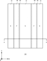
- 半導体基板のおもて面側に設けられたアノード電極と、
前記半導体基板に設けられた第1導電型のドリフト領域と、
前記アノード電極とショットキー接触された第1導電型の第1アノード領域と、
前記第1導電型と異なる第2導電型の第2アノード領域と
を備え、
前記第1アノード領域は、前記第2アノード領域のドーピング濃度以下のドーピング濃度を有し、前記第2アノード領域によって前記ドリフト領域と離間されており、
前記第1アノード領域の面積は、前記半導体基板のおもて面において、前記第2アノード領域の面積よりも大きい
半導体装置。 - 半導体基板のおもて面側に設けられたアノード電極と、
前記半導体基板に設けられた第1導電型のドリフト領域と、
前記アノード電極とショットキー接触された第1導電型の第1アノード領域と、
前記第1導電型と異なる第2導電型の第2アノード領域と
を備え、
前記第1アノード領域は、前記第2アノード領域のドーピング濃度以下のドーピング濃度を有し、前記第2アノード領域によって前記ドリフト領域と離間されており、
前記第1アノード領域の下端の深さは、前記第2アノード領域の下端の深さの半分よりも浅い
半導体装置。 - 半導体基板のおもて面側に設けられたアノード電極と、
前記半導体基板に設けられた第1導電型のドリフト領域と、
前記アノード電極とショットキー接触された第1導電型の第1アノード領域と、
前記第1導電型と異なる第2導電型の第2アノード領域と
を備え、
前記第1アノード領域は、前記第2アノード領域のドーピング濃度以下のドーピング濃度を有し、前記第2アノード領域によって前記ドリフト領域と離間されており、
前記第1アノード領域の下端の深さは、前記第2アノード領域の下端の深さの半分よりも深く、前記第2アノード領域の下端の深さよりも浅い
半導体装置。 - 半導体基板のおもて面側に設けられたアノード電極と、
前記半導体基板に設けられた第1導電型のドリフト領域と、
前記アノード電極とショットキー接触された第1導電型の第1アノード領域と、
前記第1導電型と異なる第2導電型の第2アノード領域と
を備え、
前記第1アノード領域は、前記第2アノード領域のドーピング濃度以下のドーピング濃度を有し、前記第2アノード領域によって前記ドリフト領域と離間されており、
前記第1アノード領域の下方における前記第2アノード領域の深さ方向の厚さは、0.5μm以上である
半導体装置。 - 半導体基板のおもて面側に設けられたアノード電極と、
前記半導体基板に設けられた第1導電型のドリフト領域と、
前記アノード電極とショットキー接触された第1導電型の第1アノード領域と、
前記第1導電型と異なる第2導電型の第2アノード領域と
を備え、
前記第1アノード領域は、前記第2アノード領域のドーピング濃度以下のドーピング濃度を有し、前記第2アノード領域によって前記ドリフト領域と離間されており、
前記アノード電極と接触する領域における前記第2アノード領域の下端の深さは、前記第1アノード領域の下方に設けられた前記第2アノード領域の下端の深さよりも浅い
半導体装置。 - 前記第2アノード領域の下端の最も浅い部分は、上面視において、前記第2アノード領域が前記アノード電極と接触する領域の中央に位置する
請求項5に記載の半導体装置。 - 前記アノード電極に接する前記第2アノード領域のドーピング濃度は、前記第1アノード領域のドーピング濃度よりも低い。
請求項5または6に記載の半導体装置。 - 半導体基板のおもて面側に設けられたアノード電極と、
前記半導体基板に設けられた第1導電型のドリフト領域と、
前記アノード電極とショットキー接触された第1導電型の第1アノード領域と、
前記第1導電型と異なる第2導電型の第2アノード領域と
を備え、
前記第1アノード領域は、前記第2アノード領域のドーピング濃度以下のドーピング濃度を有し、前記第2アノード領域によって前記ドリフト領域と離間されており、
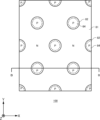
複数のトレンチ部を更に備え、
前記第1アノード領域は、前記複数のトレンチ部の間に設けられた前記半導体基板のメサ部に設けられ、当該メサ部の両端の前記複数のトレンチ部と接し、
前記第1アノード領域および前記第2アノード領域は、メサ長手方向において、交互に並んで設けられる
半導体装置。 - 半導体基板のおもて面側に設けられたアノード電極と、
前記半導体基板に設けられた第1導電型のドリフト領域と、
前記アノード電極とショットキー接触された第1導電型の第1アノード領域と、
前記第1導電型と異なる第2導電型の第2アノード領域と
を備え、
前記第1アノード領域は、前記第2アノード領域のドーピング濃度以下のドーピング濃度を有し、前記第2アノード領域によって前記ドリフト領域と離間されており、
複数のトレンチ部を更に備え、
前記第1アノード領域は、前記複数のトレンチ部の間に設けられた前記半導体基板のメサ部に設けられ、当該メサ部の両端の前記複数のトレンチ部と接し、
前記第2アノード領域の面積は、前記半導体基板のおもて面において、前記複数のトレンチ部に挟まれたメサ部の全面積の1%以下である
半導体装置。 - 半導体基板のおもて面側に設けられたアノード電極と、
前記半導体基板に設けられた第1導電型のドリフト領域と、
前記アノード電極とショットキー接触された第1導電型の第1アノード領域と、
前記第1導電型と異なる第2導電型の第2アノード領域と
を備え、
前記第1アノード領域は、前記第2アノード領域のドーピング濃度以下のドーピング濃度を有し、前記第2アノード領域によって前記ドリフト領域と離間されており、
複数のトレンチ部を更に備え、
前記第1アノード領域は、前記複数のトレンチ部の間に設けられた前記半導体基板のメサ部に設けられ、当該メサ部の両端の前記複数のトレンチ部と接し、
前記第2アノード領域の上面は、前記複数のトレンチ部に挟まれた複数のメサ部のいずれかのメサ部において、前記第1アノード領域に全面が覆われる
半導体装置。 - 半導体基板のおもて面側に設けられたアノード電極と、
前記半導体基板に設けられた第1導電型のドリフト領域と、
前記アノード電極とショットキー接触された第1導電型の第1アノード領域と、
前記第1導電型と異なる第2導電型の第2アノード領域と
を備え、
前記第1アノード領域は、前記第2アノード領域のドーピング濃度以下のドーピング濃度を有し、前記第2アノード領域によって前記ドリフト領域と離間されており、
複数のトレンチ部を更に備え、
前記第1アノード領域は、前記複数のトレンチ部の間に設けられた前記半導体基板のメサ部に設けられ、当該メサ部の両端の前記複数のトレンチ部と接し、
前記複数のトレンチ部は、前記半導体基板のおもて面から裏面に向けて徐々にトレンチ幅が大きくなる構造を有し、
前記おもて面における前記メサ部の幅は、前記複数のトレンチ部の最大のトレンチ幅よりも小さい
半導体装置。 - 半導体基板のおもて面側に設けられたアノード電極と、
前記半導体基板に設けられた第1導電型のドリフト領域と、
前記アノード電極とショットキー接触された第1導電型の第1アノード領域と、
前記第1導電型と異なる第2導電型の第2アノード領域と
を備え、
前記第1アノード領域は、前記第2アノード領域のドーピング濃度以下のドーピング濃度を有し、前記第2アノード領域によって前記ドリフト領域と離間されており、
複数のトレンチ部を更に備え、
前記第1アノード領域は、前記複数のトレンチ部の間に設けられた前記半導体基板のメサ部に設けられ、当該メサ部の両端の前記複数のトレンチ部と接し、
前記ドリフト領域よりドーピング濃度の高い第1導電型である複数の蓄積領域を備え、
前記第1アノード領域の下端の深さは、前記第2アノード領域の下端の深さの半分よりも深く、
前記第2アノード領域の下端の深さは、前記複数の蓄積領域の上端から下端までの厚みよりも小さい
半導体装置。 - 前記複数の蓄積領域のうち最も深い蓄積領域の下端は、
前記複数のトレンチ部のうち隣接するトレンチ部の半分の深さ位置よりも深く、
前記トレンチ部が前記半導体基板の裏面に向かって延伸する側壁領域と、前記トレンチ部の底部に向かって前記トレンチ部の幅が減少する底部領域との境界と同一またはそれよりも浅い
請求項12に記載の半導体装置。 - 半導体基板のおもて面側に設けられたアノード電極と、
前記半導体基板に設けられた第1導電型のドリフト領域と、
前記アノード電極とショットキー接触された第1導電型の第1アノード領域と、
前記第1導電型と異なる第2導電型の第2アノード領域と
を備え、
前記第1アノード領域は、前記第2アノード領域のドーピング濃度以下のドーピング濃度を有し、前記第2アノード領域によって前記ドリフト領域と離間されており、
複数のトレンチ部を更に備え、
前記第1アノード領域は、前記複数のトレンチ部の間に設けられた前記半導体基板のメサ部に設けられ、当該メサ部の両端の前記複数のトレンチ部と接し、
前記ドリフト領域よりドーピング濃度の高い第1導電型である蓄積領域を備え、
前記蓄積領域の下端は、
前記複数のトレンチ部のうち隣接するトレンチ部の半分の深さ位置よりも深く、
前記トレンチ部が前記半導体基板の裏面に向かって延伸する側壁領域と、前記トレンチ部の底部に向かって前記トレンチ部の幅が減少する底部領域との境界と同一またはそれよりも浅く、
前記第1アノード領域の下端の深さは、前記第2アノード領域の下端の深さの半分よりも深く、
前記第2アノード領域の下端の深さは、前記蓄積領域の上端から下端までの厚みよりも小さい
半導体装置。 - 半導体基板のおもて面側に設けられたアノード電極と、
前記半導体基板に設けられた第1導電型のドリフト領域と、
前記アノード電極とショットキー接触された第1導電型の第1アノード領域と、
前記第1導電型と異なる第2導電型の第2アノード領域と
を備え、
前記第1アノード領域は、前記第2アノード領域のドーピング濃度以下のドーピング濃度を有し、前記第2アノード領域によって前記ドリフト領域と離間されており、
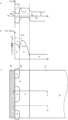
前記アノード電極に接触する第2導電型のコンタクト領域を備え、
前記コンタクト領域は、上面視で、前記第2アノード領域が前記コンタクト領域と前記第1アノード領域との間において前記おもて面に露出することにより、前記第1アノード領域と離間されている
半導体装置。 - 半導体基板のおもて面側に設けられたアノード電極と、
前記半導体基板に設けられた第1導電型のドリフト領域と、
前記アノード電極とショットキー接触された第1導電型の第1アノード領域と、
前記第1導電型と異なる第2導電型の第2アノード領域と
を備え、
前記第1アノード領域は、前記第2アノード領域のドーピング濃度以下のドーピング濃度を有し、前記第2アノード領域によって前記ドリフト領域と離間されており、
前記第1アノード領域の側面および下面は、前記第2アノード領域によって覆われている
半導体装置。 - 前記ドリフト領域よりドーピング濃度の高い第1導電型の蓄積領域を備え、
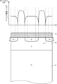
前記蓄積領域は、前記第1アノード領域および前記第2アノード領域の下方に設けられる
請求項1から11、15および16のいずれか一項に記載の半導体装置。 - 前記半導体基板の裏面側に設けられたカソード電極と、
前記半導体基板の裏面において、前記カソード電極と接して設けられたカソード層とを備え、
前記カソード層は、
第1導電型の第1カソード領域と、
前記第1カソード領域と隣接して設けられた第2導電型の第2カソード領域と
を含む
請求項1から17のいずれか一項に記載の半導体装置。 - 前記第2カソード領域の面積は、前記半導体基板の裏面において、前記第1カソード領域の面積よりも大きい
請求項18に記載の半導体装置。 - 前記第1カソード領域の面積は、前記半導体基板の裏面において、前記第1カソード領域および前記第2カソード領域の合計面積の10%以下である
請求項18または19に記載の半導体装置。 - 前記カソード層は、
前記半導体基板に設けられた裏面側カソード部と、
前記裏面側カソード部よりも前記半導体基板のおもて面側に設けられた、第2導電型のおもて面側カソード部を備え、
前記裏面側カソード部は、前記第1カソード領域および前記第2カソード領域の繰り返し構造を含む
請求項18から20のいずれか一項に記載の半導体装置。 - 前記おもて面側カソード部は、前記第1カソード領域および前記第2カソード領域と隣接して設けられ、前記第1カソード領域のおもて面側に設けられた開口を有する
請求項21に記載の半導体装置。 - 前記開口の直径Dは、前記第1カソード領域のトレンチ配列方向の幅Cよりも小さい
請求項22に記載の半導体装置。 - 前記第1アノード領域と前記アノード電極とを接続するための接続部を備え、
前記接続部は、Ti、V、Ni、およびPtの少なくとも1つを含む
請求項1から23のいずれか一項に記載の半導体装置。 - 前記半導体基板に設けられたトランジスタ部を更に備える
請求項1から24のいずれか一項に記載の半導体装置。 - 前記第1アノード領域のドーピング濃度は、1E15cm -3 以上、1E18cm -3 以下である
請求項1から25のいずれか一項に記載の半導体装置。 - 半導体基板のおもて面側に、アノード電極を設ける段階と、
前記半導体基板に、第1導電型のドリフト領域を設ける段階と、
前記アノード電極とショットキー接触された第1導電型の第1アノード領域を設ける段階と、
前記第1導電型と異なる第2導電型の第2アノード領域を設ける段階と
を備え、
前記第1アノード領域は、前記第2アノード領域のドーピング濃度以下のドーピング濃度を有し、前記第2アノード領域によって前記ドリフト領域と離間されており、
前記第1アノード領域の面積は、前記半導体基板のおもて面において、前記第2アノード領域の面積よりも大きい
半導体装置の製造方法。
Applications Claiming Priority (2)
| Application Number | Priority Date | Filing Date | Title |
|---|---|---|---|
| JP2019148604 | 2019-08-13 | ||
| JP2019148604 | 2019-08-13 |
Publications (2)
| Publication Number | Publication Date |
|---|---|
| JP2021034726A JP2021034726A (ja) | 2021-03-01 |
| JP7585646B2 true JP7585646B2 (ja) | 2024-11-19 |
Family
ID=74567556
Family Applications (1)
| Application Number | Title | Priority Date | Filing Date |
|---|---|---|---|
| JP2020131895A Active JP7585646B2 (ja) | 2019-08-13 | 2020-08-03 | 半導体装置および半導体装置の製造方法 |
Country Status (2)
| Country | Link |
|---|---|
| US (3) | US11362202B2 (ja) |
| JP (1) | JP7585646B2 (ja) |
Families Citing this family (10)
| Publication number | Priority date | Publication date | Assignee | Title |
|---|---|---|---|---|
| JP7247930B2 (ja) * | 2020-03-10 | 2023-03-29 | 株式会社デンソー | 半導体装置 |
| JP7257984B2 (ja) * | 2020-03-24 | 2023-04-14 | 株式会社東芝 | 半導体装置及びその製造方法 |
| CN113571577B (zh) * | 2021-06-04 | 2023-07-04 | 西安电子科技大学 | 一种由肖特基结势垒控制的逆导型绝缘栅双极型晶体管及其制作方法 |
| JP7574161B2 (ja) * | 2021-09-22 | 2024-10-28 | 株式会社東芝 | 半導体装置 |
| CN114203830B (zh) * | 2021-11-30 | 2023-02-24 | 深圳基本半导体有限公司 | 一种frd结构及其制作方法和应用 |
| WO2023176907A1 (ja) * | 2022-03-16 | 2023-09-21 | 富士電機株式会社 | 半導体装置 |
| JP2024089750A (ja) * | 2022-12-22 | 2024-07-04 | 株式会社 日立パワーデバイス | 半導体装置 |
| CN120814351A (zh) * | 2023-03-16 | 2025-10-17 | 罗姆股份有限公司 | 半导体器件 |
| JP2024162687A (ja) * | 2023-05-11 | 2024-11-21 | 株式会社デンソー | 半導体装置とその製造方法 |
| WO2025225266A1 (ja) * | 2024-04-26 | 2025-10-30 | 株式会社デンソー | 半導体装置および半導体装置の製造方法 |
Citations (2)
| Publication number | Priority date | Publication date | Assignee | Title |
|---|---|---|---|---|
| JP2014135419A (ja) | 2013-01-11 | 2014-07-24 | Toyota Central R&D Labs Inc | ダイオード及びダイオードを内蔵した半導体装置 |
| JP2019125763A (ja) | 2018-01-19 | 2019-07-25 | ローム株式会社 | 半導体装置 |
Family Cites Families (17)
| Publication number | Priority date | Publication date | Assignee | Title |
|---|---|---|---|---|
| JP3321185B2 (ja) | 1990-09-28 | 2002-09-03 | 株式会社東芝 | 高耐圧半導体装置 |
| US20020121663A1 (en) * | 2001-03-05 | 2002-09-05 | Semiconductor Components Industries, Llc | Semiconductor device and method |
| JP4609656B2 (ja) * | 2005-12-14 | 2011-01-12 | サンケン電気株式会社 | トレンチ構造半導体装置 |
| CN102148240B (zh) * | 2011-03-10 | 2012-08-29 | 电子科技大学 | 一种具有分裂阳极结构的soi-ligbt器件 |
| JP6001735B2 (ja) | 2011-07-27 | 2016-10-05 | 株式会社豊田中央研究所 | Mosfet |
| JP5609939B2 (ja) * | 2011-09-27 | 2014-10-22 | 株式会社デンソー | 半導体装置 |
| JP6154292B2 (ja) * | 2013-11-06 | 2017-06-28 | トヨタ自動車株式会社 | 半導体装置及び半導体装置の製造方法 |
| KR20150076716A (ko) * | 2013-12-27 | 2015-07-07 | 삼성전기주식회사 | 전력 반도체 소자 |
| JP6320808B2 (ja) * | 2014-03-19 | 2018-05-09 | 富士電機株式会社 | トレンチmos型半導体装置 |
| JP6271356B2 (ja) * | 2014-07-07 | 2018-01-31 | 株式会社東芝 | 半導体装置の製造方法 |
| JP6221974B2 (ja) * | 2014-07-14 | 2017-11-01 | トヨタ自動車株式会社 | 半導体装置 |
| JP6003961B2 (ja) * | 2014-11-04 | 2016-10-05 | トヨタ自動車株式会社 | 半導体装置 |
| JP6164201B2 (ja) | 2014-11-17 | 2017-07-19 | トヨタ自動車株式会社 | 半導体装置 |
| JP6222140B2 (ja) | 2015-03-04 | 2017-11-01 | トヨタ自動車株式会社 | 半導体装置 |
| CN108140674B (zh) * | 2015-10-16 | 2021-02-19 | 三菱电机株式会社 | 半导体装置 |
| DE102017118665A1 (de) * | 2017-08-16 | 2019-02-21 | Infineon Technologies Ag | Rc-igbt |
| DE102021125271A1 (de) | 2021-09-29 | 2023-03-30 | Infineon Technologies Ag | LeistungshalbleitervorrichtungVerfahren zur Herstellung einer Leistungshalbleitervorrichtung |
-
2020
- 2020-08-03 JP JP2020131895A patent/JP7585646B2/ja active Active
- 2020-08-13 US US16/992,143 patent/US11362202B2/en active Active
-
2022
- 2022-05-31 US US17/829,306 patent/US11894258B2/en active Active
-
2023
- 2023-12-14 US US18/539,304 patent/US20240162078A1/en active Pending
Patent Citations (2)
| Publication number | Priority date | Publication date | Assignee | Title |
|---|---|---|---|---|
| JP2014135419A (ja) | 2013-01-11 | 2014-07-24 | Toyota Central R&D Labs Inc | ダイオード及びダイオードを内蔵した半導体装置 |
| JP2019125763A (ja) | 2018-01-19 | 2019-07-25 | ローム株式会社 | 半導体装置 |
Also Published As
| Publication number | Publication date |
|---|---|
| JP2021034726A (ja) | 2021-03-01 |
| US20240162078A1 (en) | 2024-05-16 |
| US20220293775A1 (en) | 2022-09-15 |
| US11894258B2 (en) | 2024-02-06 |
| US11362202B2 (en) | 2022-06-14 |
| US20210050345A1 (en) | 2021-02-18 |
Similar Documents
| Publication | Publication Date | Title |
|---|---|---|
| JP7585646B2 (ja) | 半導体装置および半導体装置の製造方法 | |
| JP7655354B2 (ja) | 半導体装置および半導体装置の製造方法 | |
| US11094810B2 (en) | Semiconductor device and manufacturing method of semiconductor device | |
| US20220271152A1 (en) | Semiconductor device and manufacturing method thereof | |
| JP7758079B2 (ja) | 半導体装置 | |
| JP7687114B2 (ja) | 半導体装置 | |
| CN113937159A (zh) | 半导体装置 | |
| JP7750090B2 (ja) | 半導体装置およびその製造方法 | |
| JP5370985B2 (ja) | Jbsの製造方法 | |
| JP2025107491A (ja) | 超接合半導体装置 | |
| CN115132833A (zh) | 半导体装置及半导体装置的制造方法 | |
| JP2025109577A (ja) | 半導体装置 | |
| JP7332543B2 (ja) | 半導体装置 | |
| JP2024098458A (ja) | 半導体装置 | |
| JP7677444B2 (ja) | 半導体装置の製造方法および半導体装置 | |
| JP7670132B2 (ja) | 半導体装置および半導体装置の製造方法 | |
| JP7758644B2 (ja) | 半導体装置及び半導体装置の製造方法 | |
| JP7677531B2 (ja) | 半導体装置および半導体装置の製造方法 | |
| JP7506628B2 (ja) | 半導体装置 | |
| US20240072110A1 (en) | Semiconductor device and manufacturing method of semiconductor device | |
| JP2024084070A (ja) | 半導体装置 | |
| WO2024166493A1 (ja) | 半導体装置 | |
| WO2024166492A1 (ja) | 半導体装置 | |
| WO2024166494A1 (ja) | 半導体装置 | |
| JP2024097277A (ja) | 半導体装置 |
Legal Events
| Date | Code | Title | Description |
|---|---|---|---|
| A621 | Written request for application examination |
Free format text: JAPANESE INTERMEDIATE CODE: A621 Effective date: 20230713 |
|
| A977 | Report on retrieval |
Free format text: JAPANESE INTERMEDIATE CODE: A971007 Effective date: 20240514 |
|
| A131 | Notification of reasons for refusal |
Free format text: JAPANESE INTERMEDIATE CODE: A131 Effective date: 20240521 |
|
| A521 | Request for written amendment filed |
Free format text: JAPANESE INTERMEDIATE CODE: A523 Effective date: 20240718 |
|
| TRDD | Decision of grant or rejection written | ||
| A01 | Written decision to grant a patent or to grant a registration (utility model) |
Free format text: JAPANESE INTERMEDIATE CODE: A01 Effective date: 20241008 |
|
| A61 | First payment of annual fees (during grant procedure) |
Free format text: JAPANESE INTERMEDIATE CODE: A61 Effective date: 20241021 |
|
| R150 | Certificate of patent or registration of utility model |
Ref document number: 7585646 Country of ref document: JP Free format text: JAPANESE INTERMEDIATE CODE: R150 |