JP7004397B2 - 光学装置 - Google Patents
光学装置 Download PDFInfo
- Publication number
- JP7004397B2 JP7004397B2 JP2017114141A JP2017114141A JP7004397B2 JP 7004397 B2 JP7004397 B2 JP 7004397B2 JP 2017114141 A JP2017114141 A JP 2017114141A JP 2017114141 A JP2017114141 A JP 2017114141A JP 7004397 B2 JP7004397 B2 JP 7004397B2
- Authority
- JP
- Japan
- Prior art keywords
- conductive portion
- conductive
- optical element
- layer
- substrate
- Prior art date
- Legal status (The legal status is an assumption and is not a legal conclusion. Google has not performed a legal analysis and makes no representation as to the accuracy of the status listed.)
- Active
Links
Images


Classifications
-
- H—ELECTRICITY
- H10—SEMICONDUCTOR DEVICES; ELECTRIC SOLID-STATE DEVICES NOT OTHERWISE PROVIDED FOR
- H10H—INORGANIC LIGHT-EMITTING SEMICONDUCTOR DEVICES HAVING POTENTIAL BARRIERS
- H10H20/00—Individual inorganic light-emitting semiconductor devices having potential barriers, e.g. light-emitting diodes [LED]
- H10H20/80—Constructional details
- H10H20/85—Packages
- H10H20/857—Interconnections, e.g. lead-frames, bond wires or solder balls
-
- H—ELECTRICITY
- H10—SEMICONDUCTOR DEVICES; ELECTRIC SOLID-STATE DEVICES NOT OTHERWISE PROVIDED FOR
- H10W—GENERIC PACKAGES, INTERCONNECTIONS, CONNECTORS OR OTHER CONSTRUCTIONAL DETAILS OF DEVICES COVERED BY CLASS H10
- H10W72/00—Interconnections or connectors in packages
- H10W72/01—Manufacture or treatment
- H10W72/0198—Manufacture or treatment batch processes
-
- H—ELECTRICITY
- H10—SEMICONDUCTOR DEVICES; ELECTRIC SOLID-STATE DEVICES NOT OTHERWISE PROVIDED FOR
- H10W—GENERIC PACKAGES, INTERCONNECTIONS, CONNECTORS OR OTHER CONSTRUCTIONAL DETAILS OF DEVICES COVERED BY CLASS H10
- H10W74/00—Encapsulations, e.g. protective coatings
- H10W74/10—Encapsulations, e.g. protective coatings characterised by their shape or disposition
-
- H—ELECTRICITY
- H10—SEMICONDUCTOR DEVICES; ELECTRIC SOLID-STATE DEVICES NOT OTHERWISE PROVIDED FOR
- H10H—INORGANIC LIGHT-EMITTING SEMICONDUCTOR DEVICES HAVING POTENTIAL BARRIERS
- H10H20/00—Individual inorganic light-emitting semiconductor devices having potential barriers, e.g. light-emitting diodes [LED]
- H10H20/01—Manufacture or treatment
- H10H20/036—Manufacture or treatment of packages
- H10H20/0362—Manufacture or treatment of packages of encapsulations
-
- H—ELECTRICITY
- H10—SEMICONDUCTOR DEVICES; ELECTRIC SOLID-STATE DEVICES NOT OTHERWISE PROVIDED FOR
- H10H—INORGANIC LIGHT-EMITTING SEMICONDUCTOR DEVICES HAVING POTENTIAL BARRIERS
- H10H20/00—Individual inorganic light-emitting semiconductor devices having potential barriers, e.g. light-emitting diodes [LED]
- H10H20/01—Manufacture or treatment
- H10H20/036—Manufacture or treatment of packages
- H10H20/0364—Manufacture or treatment of packages of interconnections
-
- H—ELECTRICITY
- H10—SEMICONDUCTOR DEVICES; ELECTRIC SOLID-STATE DEVICES NOT OTHERWISE PROVIDED FOR
- H10H—INORGANIC LIGHT-EMITTING SEMICONDUCTOR DEVICES HAVING POTENTIAL BARRIERS
- H10H20/00—Individual inorganic light-emitting semiconductor devices having potential barriers, e.g. light-emitting diodes [LED]
- H10H20/01—Manufacture or treatment
- H10H20/036—Manufacture or treatment of packages
- H10H20/0365—Manufacture or treatment of packages of means for heat extraction or cooling
-
- H—ELECTRICITY
- H10—SEMICONDUCTOR DEVICES; ELECTRIC SOLID-STATE DEVICES NOT OTHERWISE PROVIDED FOR
- H10H—INORGANIC LIGHT-EMITTING SEMICONDUCTOR DEVICES HAVING POTENTIAL BARRIERS
- H10H20/00—Individual inorganic light-emitting semiconductor devices having potential barriers, e.g. light-emitting diodes [LED]
- H10H20/80—Constructional details
- H10H20/85—Packages
- H10H20/8506—Containers
-
- H—ELECTRICITY
- H10—SEMICONDUCTOR DEVICES; ELECTRIC SOLID-STATE DEVICES NOT OTHERWISE PROVIDED FOR
- H10H—INORGANIC LIGHT-EMITTING SEMICONDUCTOR DEVICES HAVING POTENTIAL BARRIERS
- H10H20/00—Individual inorganic light-emitting semiconductor devices having potential barriers, e.g. light-emitting diodes [LED]
- H10H20/80—Constructional details
- H10H20/85—Packages
- H10H20/852—Encapsulations
- H10H20/853—Encapsulations characterised by their shape
-
- H—ELECTRICITY
- H10—SEMICONDUCTOR DEVICES; ELECTRIC SOLID-STATE DEVICES NOT OTHERWISE PROVIDED FOR
- H10H—INORGANIC LIGHT-EMITTING SEMICONDUCTOR DEVICES HAVING POTENTIAL BARRIERS
- H10H20/00—Individual inorganic light-emitting semiconductor devices having potential barriers, e.g. light-emitting diodes [LED]
- H10H20/80—Constructional details
- H10H20/85—Packages
- H10H20/855—Optical field-shaping means, e.g. lenses
- H10H20/856—Reflecting means
-
- H—ELECTRICITY
- H10—SEMICONDUCTOR DEVICES; ELECTRIC SOLID-STATE DEVICES NOT OTHERWISE PROVIDED FOR
- H10H—INORGANIC LIGHT-EMITTING SEMICONDUCTOR DEVICES HAVING POTENTIAL BARRIERS
- H10H20/00—Individual inorganic light-emitting semiconductor devices having potential barriers, e.g. light-emitting diodes [LED]
- H10H20/80—Constructional details
- H10H20/85—Packages
- H10H20/858—Means for heat extraction or cooling
- H10H20/8585—Means for heat extraction or cooling being an interconnection
-
- H—ELECTRICITY
- H10—SEMICONDUCTOR DEVICES; ELECTRIC SOLID-STATE DEVICES NOT OTHERWISE PROVIDED FOR
- H10W—GENERIC PACKAGES, INTERCONNECTIONS, CONNECTORS OR OTHER CONSTRUCTIONAL DETAILS OF DEVICES COVERED BY CLASS H10
- H10W72/00—Interconnections or connectors in packages
- H10W72/30—Die-attach connectors
-
- H—ELECTRICITY
- H10—SEMICONDUCTOR DEVICES; ELECTRIC SOLID-STATE DEVICES NOT OTHERWISE PROVIDED FOR
- H10W—GENERIC PACKAGES, INTERCONNECTIONS, CONNECTORS OR OTHER CONSTRUCTIONAL DETAILS OF DEVICES COVERED BY CLASS H10
- H10W74/00—Encapsulations, e.g. protective coatings
-
- H—ELECTRICITY
- H10—SEMICONDUCTOR DEVICES; ELECTRIC SOLID-STATE DEVICES NOT OTHERWISE PROVIDED FOR
- H10W—GENERIC PACKAGES, INTERCONNECTIONS, CONNECTORS OR OTHER CONSTRUCTIONAL DETAILS OF DEVICES COVERED BY CLASS H10
- H10W90/00—Package configurations
-
- H—ELECTRICITY
- H10—SEMICONDUCTOR DEVICES; ELECTRIC SOLID-STATE DEVICES NOT OTHERWISE PROVIDED FOR
- H10W—GENERIC PACKAGES, INTERCONNECTIONS, CONNECTORS OR OTHER CONSTRUCTIONAL DETAILS OF DEVICES COVERED BY CLASS H10
- H10W90/00—Package configurations
- H10W90/701—Package configurations characterised by the relative positions of pads or connectors relative to package parts
- H10W90/751—Package configurations characterised by the relative positions of pads or connectors relative to package parts of bond wires
- H10W90/754—Package configurations characterised by the relative positions of pads or connectors relative to package parts of bond wires between a chip and a stacked insulating package substrate, interposer or RDL
-
- H—ELECTRICITY
- H10—SEMICONDUCTOR DEVICES; ELECTRIC SOLID-STATE DEVICES NOT OTHERWISE PROVIDED FOR
- H10W—GENERIC PACKAGES, INTERCONNECTIONS, CONNECTORS OR OTHER CONSTRUCTIONAL DETAILS OF DEVICES COVERED BY CLASS H10
- H10W90/00—Package configurations
- H10W90/701—Package configurations characterised by the relative positions of pads or connectors relative to package parts
- H10W90/751—Package configurations characterised by the relative positions of pads or connectors relative to package parts of bond wires
- H10W90/756—Package configurations characterised by the relative positions of pads or connectors relative to package parts of bond wires between a chip and a stacked lead frame, conducting package substrate or heat sink
Landscapes
- Led Device Packages (AREA)
- Light Receiving Elements (AREA)
Description
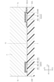
図1~図18を用いて、本発明の第1実施形態について説明する。
[付記1]
基板と、
前記基板に形成された導電層と、
前記導電層に形成された絶縁層と、
前記導電層に配置された第1光学素子と、
前記第1光学素子を覆う封止樹脂部と、を備え、
前記導電層は、第1導電箇所と、前記第1導電箇所から離間した第2導電箇所と、前記第1導電箇所から第1方向に延び出る第1導電部分と、を含み、
前記第1導電部分は、前記第2導電箇所から、前記第1方向に交差する第2方向に対し離間しており、
前記絶縁層は、前記第1導電部分に形成された第1絶縁部を含み、前記第1絶縁部は、前記第1方向において、前記第2導電箇所と重なる部位を有する、光学装置。
[付記2]
前記導電層に配置された第2光学素子を更に備え、
前記第1光学素子は、前記第1導電箇所に配置されており、
前記第2光学素子は、前記第2導電箇所に配置されている、付記1に記載の光学装置。
[付記3]
前記第1光学素子および前記第1導電箇所の間に介在する第1接合層と、
前記第2光学素子および前記第2導電箇所の間に介在する第2接合層と、を更に備え、
前記第1絶縁部は、前記第1方向において、前記第2接合層と重なる部位を有する、付記2に記載の光学装置。
[付記4]
前記第1絶縁部は、前記第1方向において、前記第2光学素子に重なる部位を有する、付記3に記載の光学装置。
[付記5]
前記基板は、前記第2方向に互いに離間する第1側面および第2側面を含み、前記第1側面および前記第2側面は、互いに反対側を向いており、
前記導電層は、前記第1導電箇所から延び出る第1追加導電部分を含み、
前記第1追加導電部分は、前記基板の厚さ方向視において、前記第1側面に至っている、付記2ないし付記4のいずれかに記載の光学装置。
[付記6]
前記第1追加導電部分は、前記基板の厚さ方向視において、前記第1方向と前記第2方向とは異なる方向に延びている、付記5に記載の光学装置。
[付記7]
前記第1追加導電部分は、前記絶縁層から露出している、付記5または付記6に記載の光学装置。
[付記8]
前記第1追加導電部分は、前記第1側面と面一である第1外側面を有する、付記5ないし付記7のいずれかに記載の光学装置。
[付記9]
前記導電層は、前記第2導電箇所から延び出る第2導電部分を含む、付記5に記載の光学装置。
[付記10]
前記導電層は、前記第1導電箇所および前記第2導電箇所から離間する第3導電箇所と、前記第3導電箇所から前記第2導電箇所とは反対側に延び出る第3導電部分と、を含み、
前記絶縁層は、前記第3導電部分に形成された第2絶縁部を含む、付記9に記載の光学装置。
[付記11]
前記導電層は、前記第3導電箇所あるいは前記第3導電部分から延び出る第2追加導電部分を含み、
前記第2追加導電部分は、前記基板の厚さ方向視において、前記第2側面に至っている、付記10に記載の光学装置。
[付記12]
前記第2追加導電部分は、前記基板の厚さ方向視において、前記第1導電部分が延びる方向と同一方向に延びている、付記11に記載の光学装置。
[付記13]
前記第2追加導電部分は、前記絶縁層から露出している、付記11または付記12に記載の光学装置。
[付記14]
前記第2追加導電部分は、前記第2側面と面一である第2外側面を有し、
前記第2追加導電部分の前記第2外側面および前記第1追加導電部分の前記第1外側面はいずれも、前記第2方向に沿って延びる仮想線であって、前記厚さ方向視における前記基板の中心を通る仮想線に対し、前記厚さ方向視において同一側に位置している、付記11ないし付記13のいずれかに記載の光学装置。
[付記15]
前記絶縁層は、前記第2追加導電部分に形成されている、付記11ないし付記14のいずれかに記載の光学装置。
[付記16]
前記第1光学素子にボンディングされた第1ワイヤと、
前記第2光学素子にボンディングされた第2ワイヤと、を更に備える、付記2ないし付記15のいずれかに記載の光学装置。
11 主面
13 裏面
15A 第1側面
15B 第2側面
15C 第3側面
15D 第4側面
3 導電層
31A 第1導電箇所
31B 第2導電箇所
31C 第3導電箇所
31D 第4導電箇所
32A 第1導電部分
32B 第2導電部分
32C 第3導電部分
32D 第4導電部分
33A 第1導電部
33B 第2導電部
33C 第3導電部
33D 第4導電部
341A 第1外側面
341C 第2外側面
34A 第1追加導電部分
34C 第2追加導電部分
34M 部位
37A 第1導電部
37B 第2導電部
37C 第3導電部
37D 第4導電部
381 箇所
382 箇所
383 箇所
384 箇所
38A 第1裏面部
38B 第2裏面部
38C 第3裏面部
38D 第4裏面部
41 第1光学素子
42 第2光学素子
43 第1ワイヤ
44 第2ワイヤ
51 第1接合層
52 第2接合層
6 絶縁層
611A 縁
61A 第1絶縁部
61C 第2絶縁部
63 部位
64 部位
65 部位
69 縁
7 封止樹脂部
71 第1外面
72 第2外面
81 絶縁層
A1 光学装置
C1 中心
L1 仮想線
X1 第1方向
Y1 第2方向
Z1 厚さ方向
Claims (14)
- 基板と、
前記基板に形成された導電層と、
前記導電層に形成された絶縁層と、
前記導電層に配置された第1光学素子と、
前記第1光学素子を覆う封止樹脂部と、を備え、
前記導電層は、第1導電箇所と、前記第1導電箇所から離間した第2導電箇所と、前記第1導電箇所から第1方向に延び出る第1導電部分と、を含み、
前記第1導電部分は、前記第2導電箇所から、前記第1方向に交差する第2方向に対し離間しており、
前記絶縁層は、前記第1導電部分に形成された第1絶縁部を含み、前記第1絶縁部は、前記第2方向に沿って見て、前記第2導電箇所と重なる部位を有し、
前記導電層に配置された第2光学素子を更に備え、
前記第1光学素子は、前記第1導電箇所に配置されており、
前記第2光学素子は、前記第2導電箇所に配置されており、
前記基板は、前記第2方向に互いに離間する第1側面および第2側面を含み、前記第1側面および前記第2側面は、互いに反対側を向いており、
前記導電層は、前記第1導電箇所から延び出る第1追加導電部分を含み、
前記第1追加導電部分は、前記基板の厚さ方向視において、前記第1側面に至っている、
光学装置。 - 前記第1光学素子および前記第1導電箇所の間に介在する第1接合層と、
前記第2光学素子および前記第2導電箇所の間に介在する第2接合層と、を更に備え、
前記第1絶縁部は、前記第2方向に沿って見て、前記第2接合層と重なる部位を有する、請求項1に記載の光学装置。 - 前記第1絶縁部は、前記第2方向に沿って見て、前記第2光学素子に重なる部位を有する、請求項2に記載の光学装置。
- 前記第1追加導電部分は、前記基板の厚さ方向視において、前記第1方向と前記第2方向とは異なる方向に延びている、請求項1に記載の光学装置。
- 前記第1追加導電部分は、前記絶縁層から露出している、請求項1または請求項2に記載の光学装置。
- 前記第1追加導電部分は、前記第1側面と面一である第1外側面を有する、請求項1ないし請求項5のいずれかに記載の光学装置。
- 前記導電層は、前記第2導電箇所から延び出る第2導電部分を含む、請求項6に記載の光学装置。
- 前記導電層は、前記第1導電箇所および前記第2導電箇所から離間する第3導電箇所と、前記第3導電箇所から前記第2導電箇所とは反対側に延び出る第3導電部分と、を含み、
前記絶縁層は、前記第3導電部分に形成された第2絶縁部を含む、請求項7に記載の光学装置。 - 前記導電層は、前記第3導電箇所あるいは前記第3導電部分から延び出る第2追加導電部分を含み、
前記第2追加導電部分は、前記基板の厚さ方向視において、前記第2側面に至っている、請求項8に記載の光学装置。 - 前記第2追加導電部分は、前記基板の厚さ方向視において、前記第1追加導電部分が延びる方向と同一方向に延びている、請求項9に記載の光学装置。
- 前記第2追加導電部分は、前記絶縁層から露出している、請求項9または請求項10に記載の光学装置。
- 前記第2追加導電部分は、前記第2側面と面一である第2外側面を有し、
前記第2追加導電部分の前記第2外側面および前記第1追加導電部分の前記第1外側面はいずれも、前記第2方向に沿って延びる仮想線であって、前記厚さ方向視における前記基板の中心を通る仮想線に対し、前記厚さ方向視において同一側に位置している、請求項9ないし請求項11のいずれかに記載の光学装置。 - 前記絶縁層は、前記第2追加導電部分に形成されている、請求項9ないし請求項12のいずれかに記載の光学装置。
- 前記第1光学素子にボンディングされた第1ワイヤと、
前記第2光学素子にボンディングされた第2ワイヤと、を更に備える、請求項1ないし請求項13のいずれかに記載の光学装置。
Priority Applications (2)
| Application Number | Priority Date | Filing Date | Title |
|---|---|---|---|
| JP2017114141A JP7004397B2 (ja) | 2017-06-09 | 2017-06-09 | 光学装置 |
| US16/002,219 US10439117B2 (en) | 2017-06-09 | 2018-06-07 | Optical device |
Applications Claiming Priority (1)
| Application Number | Priority Date | Filing Date | Title |
|---|---|---|---|
| JP2017114141A JP7004397B2 (ja) | 2017-06-09 | 2017-06-09 | 光学装置 |
Publications (2)
| Publication Number | Publication Date |
|---|---|
| JP2018207063A JP2018207063A (ja) | 2018-12-27 |
| JP7004397B2 true JP7004397B2 (ja) | 2022-01-21 |
Family
ID=64563671
Family Applications (1)
| Application Number | Title | Priority Date | Filing Date |
|---|---|---|---|
| JP2017114141A Active JP7004397B2 (ja) | 2017-06-09 | 2017-06-09 | 光学装置 |
Country Status (2)
| Country | Link |
|---|---|
| US (1) | US10439117B2 (ja) |
| JP (1) | JP7004397B2 (ja) |
Citations (14)
| Publication number | Priority date | Publication date | Assignee | Title |
|---|---|---|---|---|
| JP2000183406A (ja) | 1998-12-15 | 2000-06-30 | Matsushita Electric Works Ltd | 発光ダイオード |
| JP2002314143A (ja) | 2001-04-09 | 2002-10-25 | Toshiba Corp | 発光装置 |
| JP2003264267A (ja) | 2002-03-08 | 2003-09-19 | Rohm Co Ltd | 半導体チップを使用した半導体装置 |
| JP2005538550A (ja) | 2002-09-04 | 2005-12-15 | クリー インコーポレイテッド | 電力表面取り付けの発光ダイ・パッケージ |
| JP2008288228A (ja) | 2007-05-15 | 2008-11-27 | Sony Corp | 発光装置、光源装置、及び液晶表示装置 |
| WO2009011302A1 (ja) | 2007-07-13 | 2009-01-22 | Rohm Co., Ltd. | Ledモジュールおよびledドットマトリクス表示装置 |
| JP2009105198A (ja) | 2007-10-23 | 2009-05-14 | Sanyo Electric Co Ltd | プリント配線基板およびそれを備えた発光装置 |
| JP2011003798A (ja) | 2009-06-19 | 2011-01-06 | Japan Aviation Electronics Industry Ltd | 電気接続部材およびそれを用いたソケットコネクタ |
| US20110156090A1 (en) | 2008-03-25 | 2011-06-30 | Lin Charles W C | Semiconductor chip assembly with post/base/post heat spreader and asymmetric posts |
| JP2012517709A (ja) | 2009-02-12 | 2012-08-02 | オスラム オプト セミコンダクターズ ゲゼルシャフト ミット ベシュレンクテル ハフツング | 半導体構造および半導体構造の製造方法 |
| JP2012186450A (ja) | 2011-02-16 | 2012-09-27 | Rohm Co Ltd | Ledモジュール |
| JP2014160756A (ja) | 2013-02-20 | 2014-09-04 | Stanley Electric Co Ltd | 発光素子モジュール |
| JP2015115432A (ja) | 2013-12-11 | 2015-06-22 | ローム株式会社 | 半導体装置 |
| JP2015201605A (ja) | 2014-04-10 | 2015-11-12 | 日亜化学工業株式会社 | 発光装置及び発光装置の製造方法 |
Family Cites Families (2)
| Publication number | Priority date | Publication date | Assignee | Title |
|---|---|---|---|---|
| JP2002314138A (ja) * | 2001-04-09 | 2002-10-25 | Toshiba Corp | 発光装置 |
| KR101380390B1 (ko) * | 2013-06-28 | 2014-04-02 | 서울반도체 주식회사 | 방습 led 패키지 |
-
2017
- 2017-06-09 JP JP2017114141A patent/JP7004397B2/ja active Active
-
2018
- 2018-06-07 US US16/002,219 patent/US10439117B2/en active Active
Patent Citations (14)
| Publication number | Priority date | Publication date | Assignee | Title |
|---|---|---|---|---|
| JP2000183406A (ja) | 1998-12-15 | 2000-06-30 | Matsushita Electric Works Ltd | 発光ダイオード |
| JP2002314143A (ja) | 2001-04-09 | 2002-10-25 | Toshiba Corp | 発光装置 |
| JP2003264267A (ja) | 2002-03-08 | 2003-09-19 | Rohm Co Ltd | 半導体チップを使用した半導体装置 |
| JP2005538550A (ja) | 2002-09-04 | 2005-12-15 | クリー インコーポレイテッド | 電力表面取り付けの発光ダイ・パッケージ |
| JP2008288228A (ja) | 2007-05-15 | 2008-11-27 | Sony Corp | 発光装置、光源装置、及び液晶表示装置 |
| WO2009011302A1 (ja) | 2007-07-13 | 2009-01-22 | Rohm Co., Ltd. | Ledモジュールおよびledドットマトリクス表示装置 |
| JP2009105198A (ja) | 2007-10-23 | 2009-05-14 | Sanyo Electric Co Ltd | プリント配線基板およびそれを備えた発光装置 |
| US20110156090A1 (en) | 2008-03-25 | 2011-06-30 | Lin Charles W C | Semiconductor chip assembly with post/base/post heat spreader and asymmetric posts |
| JP2012517709A (ja) | 2009-02-12 | 2012-08-02 | オスラム オプト セミコンダクターズ ゲゼルシャフト ミット ベシュレンクテル ハフツング | 半導体構造および半導体構造の製造方法 |
| JP2011003798A (ja) | 2009-06-19 | 2011-01-06 | Japan Aviation Electronics Industry Ltd | 電気接続部材およびそれを用いたソケットコネクタ |
| JP2012186450A (ja) | 2011-02-16 | 2012-09-27 | Rohm Co Ltd | Ledモジュール |
| JP2014160756A (ja) | 2013-02-20 | 2014-09-04 | Stanley Electric Co Ltd | 発光素子モジュール |
| JP2015115432A (ja) | 2013-12-11 | 2015-06-22 | ローム株式会社 | 半導体装置 |
| JP2015201605A (ja) | 2014-04-10 | 2015-11-12 | 日亜化学工業株式会社 | 発光装置及び発光装置の製造方法 |
Also Published As
| Publication number | Publication date |
|---|---|
| US10439117B2 (en) | 2019-10-08 |
| JP2018207063A (ja) | 2018-12-27 |
| US20180358524A1 (en) | 2018-12-13 |
Similar Documents
| Publication | Publication Date | Title |
|---|---|---|
| CN102683509B (zh) | Led模块 | |
| CN101459166B (zh) | 发光二极管 | |
| JP6293995B2 (ja) | 発光素子搭載用パッケージ及びその製造方法、並びに発光素子パッケージ | |
| JP6483800B2 (ja) | 発光素子搭載用パッケージ、発光装置および発光モジュール | |
| JP6855787B2 (ja) | 発光素子 | |
| JP7283938B2 (ja) | 半導体発光装置 | |
| JP2013161903A (ja) | 半導体装置およびその製造方法 | |
| US9537019B2 (en) | Semiconductor device | |
| TWI455363B (zh) | 發光二極體封裝結構及其製造方法 | |
| KR20130051206A (ko) | 발광소자 모듈 | |
| JP4863193B2 (ja) | 半導体発光装置 | |
| JP5745784B2 (ja) | 発光ダイオード | |
| JP5114773B2 (ja) | 表面実装型発光装置 | |
| JP2022180523A (ja) | 半導体装置 | |
| JP4831958B2 (ja) | 表面実装型led | |
| JP7004397B2 (ja) | 光学装置 | |
| JP2005353802A (ja) | 発光ダイオード | |
| JP5912471B2 (ja) | 半導体デバイス | |
| JP5809965B2 (ja) | 半導体発光素子 | |
| JP6543391B2 (ja) | 半導体装置 | |
| WO2010140693A1 (ja) | 電子部品 | |
| JP6679799B2 (ja) | 発光装置 | |
| TW201427116A (zh) | 具有傾斜結構之發光二極體封裝 | |
| JP2014022705A (ja) | 半導体発光装置及びその製造方法 | |
| JP2016032082A (ja) | メッキ膜の剥離防止方法、部品集合体および発光装置 |
Legal Events
| Date | Code | Title | Description |
|---|---|---|---|
| A621 | Written request for application examination |
Free format text: JAPANESE INTERMEDIATE CODE: A621 Effective date: 20200511 |
|
| A977 | Report on retrieval |
Free format text: JAPANESE INTERMEDIATE CODE: A971007 Effective date: 20210430 |
|
| A131 | Notification of reasons for refusal |
Free format text: JAPANESE INTERMEDIATE CODE: A131 Effective date: 20210511 |
|
| A521 | Request for written amendment filed |
Free format text: JAPANESE INTERMEDIATE CODE: A523 Effective date: 20210614 |
|
| TRDD | Decision of grant or rejection written | ||
| A01 | Written decision to grant a patent or to grant a registration (utility model) |
Free format text: JAPANESE INTERMEDIATE CODE: A01 Effective date: 20211130 |
|
| A61 | First payment of annual fees (during grant procedure) |
Free format text: JAPANESE INTERMEDIATE CODE: A61 Effective date: 20211224 |
|
| R150 | Certificate of patent or registration of utility model |
Ref document number: 7004397 Country of ref document: JP Free format text: JAPANESE INTERMEDIATE CODE: R150 |
|
| R250 | Receipt of annual fees |
Free format text: JAPANESE INTERMEDIATE CODE: R250 |
|
| R250 | Receipt of annual fees |
Free format text: JAPANESE INTERMEDIATE CODE: R250 |