JP6714616B2 - カーボンナノチューブ接合シートおよびカーボンナノチューブ接合シートの製造方法 - Google Patents
カーボンナノチューブ接合シートおよびカーボンナノチューブ接合シートの製造方法 Download PDFInfo
- Publication number
- JP6714616B2 JP6714616B2 JP2017559229A JP2017559229A JP6714616B2 JP 6714616 B2 JP6714616 B2 JP 6714616B2 JP 2017559229 A JP2017559229 A JP 2017559229A JP 2017559229 A JP2017559229 A JP 2017559229A JP 6714616 B2 JP6714616 B2 JP 6714616B2
- Authority
- JP
- Japan
- Prior art keywords
- sheet
- carbon nanotube
- array sheet
- cnt array
- sintered body
- Prior art date
- Legal status (The legal status is an assumption and is not a legal conclusion. Google has not performed a legal analysis and makes no representation as to the accuracy of the status listed.)
- Active
Links
Images


Classifications
-
- B—PERFORMING OPERATIONS; TRANSPORTING
- B32—LAYERED PRODUCTS
- B32B—LAYERED PRODUCTS, i.e. PRODUCTS BUILT-UP OF STRATA OF FLAT OR NON-FLAT, e.g. CELLULAR OR HONEYCOMB, FORM
- B32B9/00—Layered products comprising a layer of a particular substance not covered by groups B32B11/00 - B32B29/00
- B32B9/005—Layered products comprising a layer of a particular substance not covered by groups B32B11/00 - B32B29/00 comprising one layer of ceramic material, e.g. porcelain, ceramic tile
- B32B9/007—Layered products comprising a layer of a particular substance not covered by groups B32B11/00 - B32B29/00 comprising one layer of ceramic material, e.g. porcelain, ceramic tile comprising carbon, e.g. graphite, composite carbon
-
- B—PERFORMING OPERATIONS; TRANSPORTING
- B22—CASTING; POWDER METALLURGY
- B22F—WORKING METALLIC POWDER; MANUFACTURE OF ARTICLES FROM METALLIC POWDER; MAKING METALLIC POWDER; APPARATUS OR DEVICES SPECIALLY ADAPTED FOR METALLIC POWDER
- B22F7/00—Manufacture of composite layers, workpieces, or articles, comprising metallic powder, by sintering the powder, with or without compacting wherein at least one part is obtained by sintering or compression
- B22F7/06—Manufacture of composite layers, workpieces, or articles, comprising metallic powder, by sintering the powder, with or without compacting wherein at least one part is obtained by sintering or compression of composite workpieces or articles from parts, e.g. to form tipped tools
- B22F7/08—Manufacture of composite layers, workpieces, or articles, comprising metallic powder, by sintering the powder, with or without compacting wherein at least one part is obtained by sintering or compression of composite workpieces or articles from parts, e.g. to form tipped tools with one or more parts not made from powder
-
- B—PERFORMING OPERATIONS; TRANSPORTING
- B28—WORKING CEMENT, CLAY, OR STONE
- B28B—SHAPING CLAY OR OTHER CERAMIC COMPOSITIONS; SHAPING SLAG; SHAPING MIXTURES CONTAINING CEMENTITIOUS MATERIAL, e.g. PLASTER
- B28B11/00—Apparatus or processes for treating or working the shaped or preshaped articles
- B28B11/24—Apparatus or processes for treating or working the shaped or preshaped articles for curing, setting or hardening
- B28B11/243—Setting, e.g. drying, dehydrating or firing ceramic articles
-
- B—PERFORMING OPERATIONS; TRANSPORTING
- B32—LAYERED PRODUCTS
- B32B—LAYERED PRODUCTS, i.e. PRODUCTS BUILT-UP OF STRATA OF FLAT OR NON-FLAT, e.g. CELLULAR OR HONEYCOMB, FORM
- B32B15/00—Layered products comprising a layer of metal
- B32B15/04—Layered products comprising a layer of metal comprising metal as the main or only constituent of a layer, which is next to another layer of the same or of a different material
-
- B—PERFORMING OPERATIONS; TRANSPORTING
- B32—LAYERED PRODUCTS
- B32B—LAYERED PRODUCTS, i.e. PRODUCTS BUILT-UP OF STRATA OF FLAT OR NON-FLAT, e.g. CELLULAR OR HONEYCOMB, FORM
- B32B38/00—Ancillary operations in connection with laminating processes
- B32B38/0036—Heat treatment
-
- B—PERFORMING OPERATIONS; TRANSPORTING
- B32—LAYERED PRODUCTS
- B32B—LAYERED PRODUCTS, i.e. PRODUCTS BUILT-UP OF STRATA OF FLAT OR NON-FLAT, e.g. CELLULAR OR HONEYCOMB, FORM
- B32B5/00—Layered products characterised by the non- homogeneity or physical structure, i.e. comprising a fibrous, filamentary, particulate or foam layer; Layered products characterised by having a layer differing constitutionally or physically in different parts
- B32B5/02—Layered products characterised by the non- homogeneity or physical structure, i.e. comprising a fibrous, filamentary, particulate or foam layer; Layered products characterised by having a layer differing constitutionally or physically in different parts characterised by structural features of a fibrous or filamentary layer
-
- B—PERFORMING OPERATIONS; TRANSPORTING
- B32—LAYERED PRODUCTS
- B32B—LAYERED PRODUCTS, i.e. PRODUCTS BUILT-UP OF STRATA OF FLAT OR NON-FLAT, e.g. CELLULAR OR HONEYCOMB, FORM
- B32B9/00—Layered products comprising a layer of a particular substance not covered by groups B32B11/00 - B32B29/00
-
- B—PERFORMING OPERATIONS; TRANSPORTING
- B82—NANOTECHNOLOGY
- B82Y—SPECIFIC USES OR APPLICATIONS OF NANOSTRUCTURES; MEASUREMENT OR ANALYSIS OF NANOSTRUCTURES; MANUFACTURE OR TREATMENT OF NANOSTRUCTURES
- B82Y40/00—Manufacture or treatment of nanostructures
-
- C—CHEMISTRY; METALLURGY
- C01—INORGANIC CHEMISTRY
- C01B—NON-METALLIC ELEMENTS; COMPOUNDS THEREOF; METALLOIDS OR COMPOUNDS THEREOF NOT COVERED BY SUBCLASS C01C
- C01B32/00—Carbon; Compounds thereof
- C01B32/15—Nano-sized carbon materials
- C01B32/158—Carbon nanotubes
- C01B32/168—After-treatment
-
- C—CHEMISTRY; METALLURGY
- C09—DYES; PAINTS; POLISHES; NATURAL RESINS; ADHESIVES; COMPOSITIONS NOT OTHERWISE PROVIDED FOR; APPLICATIONS OF MATERIALS NOT OTHERWISE PROVIDED FOR
- C09K—MATERIALS FOR MISCELLANEOUS APPLICATIONS, NOT PROVIDED FOR ELSEWHERE
- C09K5/00—Heat-transfer, heat-exchange or heat-storage materials, e.g. refrigerants; Materials for the production of heat or cold by chemical reactions other than by combustion
- C09K5/08—Materials not undergoing a change of physical state when used
- C09K5/14—Solid materials, e.g. powdery or granular
-
- C—CHEMISTRY; METALLURGY
- C23—COATING METALLIC MATERIAL; COATING MATERIAL WITH METALLIC MATERIAL; CHEMICAL SURFACE TREATMENT; DIFFUSION TREATMENT OF METALLIC MATERIAL; COATING BY VACUUM EVAPORATION, BY SPUTTERING, BY ION IMPLANTATION OR BY CHEMICAL VAPOUR DEPOSITION, IN GENERAL; INHIBITING CORROSION OF METALLIC MATERIAL OR INCRUSTATION IN GENERAL
- C23C—COATING METALLIC MATERIAL; COATING MATERIAL WITH METALLIC MATERIAL; SURFACE TREATMENT OF METALLIC MATERIAL BY DIFFUSION INTO THE SURFACE, BY CHEMICAL CONVERSION OR SUBSTITUTION; COATING BY VACUUM EVAPORATION, BY SPUTTERING, BY ION IMPLANTATION OR BY CHEMICAL VAPOUR DEPOSITION, IN GENERAL
- C23C16/00—Chemical coating by decomposition of gaseous compounds, without leaving reaction products of surface material in the coating, i.e. chemical vapour deposition [CVD] processes
- C23C16/22—Chemical coating by decomposition of gaseous compounds, without leaving reaction products of surface material in the coating, i.e. chemical vapour deposition [CVD] processes characterised by the deposition of inorganic material, other than metallic material
- C23C16/26—Deposition of carbon only
-
- H—ELECTRICITY
- H01—ELECTRIC ELEMENTS
- H01L—SEMICONDUCTOR DEVICES NOT COVERED BY CLASS H10
- H01L23/00—Details of semiconductor or other solid state devices
- H01L23/34—Arrangements for cooling, heating, ventilating or temperature compensation ; Temperature sensing arrangements
- H01L23/36—Selection of materials, or shaping, to facilitate cooling or heating, e.g. heatsinks
- H01L23/373—Cooling facilitated by selection of materials for the device or materials for thermal expansion adaptation, e.g. carbon
-
- H—ELECTRICITY
- H01—ELECTRIC ELEMENTS
- H01L—SEMICONDUCTOR DEVICES NOT COVERED BY CLASS H10
- H01L24/00—Arrangements for connecting or disconnecting semiconductor or solid-state bodies; Methods or apparatus related thereto
- H01L24/01—Means for bonding being attached to, or being formed on, the surface to be connected, e.g. chip-to-package, die-attach, "first-level" interconnects; Manufacturing methods related thereto
- H01L24/26—Layer connectors, e.g. plate connectors, solder or adhesive layers; Manufacturing methods related thereto
- H01L24/27—Manufacturing methods
-
- H—ELECTRICITY
- H01—ELECTRIC ELEMENTS
- H01L—SEMICONDUCTOR DEVICES NOT COVERED BY CLASS H10
- H01L24/00—Arrangements for connecting or disconnecting semiconductor or solid-state bodies; Methods or apparatus related thereto
- H01L24/01—Means for bonding being attached to, or being formed on, the surface to be connected, e.g. chip-to-package, die-attach, "first-level" interconnects; Manufacturing methods related thereto
- H01L24/26—Layer connectors, e.g. plate connectors, solder or adhesive layers; Manufacturing methods related thereto
- H01L24/28—Structure, shape, material or disposition of the layer connectors prior to the connecting process
- H01L24/29—Structure, shape, material or disposition of the layer connectors prior to the connecting process of an individual layer connector
-
- H—ELECTRICITY
- H05—ELECTRIC TECHNIQUES NOT OTHERWISE PROVIDED FOR
- H05K—PRINTED CIRCUITS; CASINGS OR CONSTRUCTIONAL DETAILS OF ELECTRIC APPARATUS; MANUFACTURE OF ASSEMBLAGES OF ELECTRICAL COMPONENTS
- H05K7/00—Constructional details common to different types of electric apparatus
- H05K7/20—Modifications to facilitate cooling, ventilating, or heating
-
- B—PERFORMING OPERATIONS; TRANSPORTING
- B32—LAYERED PRODUCTS
- B32B—LAYERED PRODUCTS, i.e. PRODUCTS BUILT-UP OF STRATA OF FLAT OR NON-FLAT, e.g. CELLULAR OR HONEYCOMB, FORM
- B32B2305/00—Condition, form or state of the layers or laminate
- B32B2305/80—Sintered
-
- B—PERFORMING OPERATIONS; TRANSPORTING
- B82—NANOTECHNOLOGY
- B82Y—SPECIFIC USES OR APPLICATIONS OF NANOSTRUCTURES; MEASUREMENT OR ANALYSIS OF NANOSTRUCTURES; MANUFACTURE OR TREATMENT OF NANOSTRUCTURES
- B82Y30/00—Nanotechnology for materials or surface science, e.g. nanocomposites
-
- C—CHEMISTRY; METALLURGY
- C01—INORGANIC CHEMISTRY
- C01B—NON-METALLIC ELEMENTS; COMPOUNDS THEREOF; METALLOIDS OR COMPOUNDS THEREOF NOT COVERED BY SUBCLASS C01C
- C01B2202/00—Structure or properties of carbon nanotubes
- C01B2202/20—Nanotubes characterized by their properties
- C01B2202/24—Thermal properties
-
- H—ELECTRICITY
- H01—ELECTRIC ELEMENTS
- H01L—SEMICONDUCTOR DEVICES NOT COVERED BY CLASS H10
- H01L2224/00—Indexing scheme for arrangements for connecting or disconnecting semiconductor or solid-state bodies and methods related thereto as covered by H01L24/00
- H01L2224/01—Means for bonding being attached to, or being formed on, the surface to be connected, e.g. chip-to-package, die-attach, "first-level" interconnects; Manufacturing methods related thereto
- H01L2224/26—Layer connectors, e.g. plate connectors, solder or adhesive layers; Manufacturing methods related thereto
- H01L2224/27—Manufacturing methods
- H01L2224/27001—Involving a temporary auxiliary member not forming part of the manufacturing apparatus, e.g. removable or sacrificial coating, film or substrate
- H01L2224/27003—Involving a temporary auxiliary member not forming part of the manufacturing apparatus, e.g. removable or sacrificial coating, film or substrate for holding or transferring the layer preform
-
- H—ELECTRICITY
- H01—ELECTRIC ELEMENTS
- H01L—SEMICONDUCTOR DEVICES NOT COVERED BY CLASS H10
- H01L2224/00—Indexing scheme for arrangements for connecting or disconnecting semiconductor or solid-state bodies and methods related thereto as covered by H01L24/00
- H01L2224/01—Means for bonding being attached to, or being formed on, the surface to be connected, e.g. chip-to-package, die-attach, "first-level" interconnects; Manufacturing methods related thereto
- H01L2224/26—Layer connectors, e.g. plate connectors, solder or adhesive layers; Manufacturing methods related thereto
- H01L2224/27—Manufacturing methods
- H01L2224/275—Manufacturing methods by chemical or physical modification of a pre-existing or pre-deposited material
- H01L2224/27505—Sintering
-
- H—ELECTRICITY
- H01—ELECTRIC ELEMENTS
- H01L—SEMICONDUCTOR DEVICES NOT COVERED BY CLASS H10
- H01L2224/00—Indexing scheme for arrangements for connecting or disconnecting semiconductor or solid-state bodies and methods related thereto as covered by H01L24/00
- H01L2224/01—Means for bonding being attached to, or being formed on, the surface to be connected, e.g. chip-to-package, die-attach, "first-level" interconnects; Manufacturing methods related thereto
- H01L2224/26—Layer connectors, e.g. plate connectors, solder or adhesive layers; Manufacturing methods related thereto
- H01L2224/28—Structure, shape, material or disposition of the layer connectors prior to the connecting process
- H01L2224/29—Structure, shape, material or disposition of the layer connectors prior to the connecting process of an individual layer connector
- H01L2224/29001—Core members of the layer connector
- H01L2224/29099—Material
- H01L2224/291—Material with a principal constituent of the material being a metal or a metalloid, e.g. boron [B], silicon [Si], germanium [Ge], arsenic [As], antimony [Sb], tellurium [Te] and polonium [Po], and alloys thereof
- H01L2224/29138—Material with a principal constituent of the material being a metal or a metalloid, e.g. boron [B], silicon [Si], germanium [Ge], arsenic [As], antimony [Sb], tellurium [Te] and polonium [Po], and alloys thereof the principal constituent melting at a temperature of greater than or equal to 950°C and less than 1550°C
-
- H—ELECTRICITY
- H01—ELECTRIC ELEMENTS
- H01L—SEMICONDUCTOR DEVICES NOT COVERED BY CLASS H10
- H01L2224/00—Indexing scheme for arrangements for connecting or disconnecting semiconductor or solid-state bodies and methods related thereto as covered by H01L24/00
- H01L2224/01—Means for bonding being attached to, or being formed on, the surface to be connected, e.g. chip-to-package, die-attach, "first-level" interconnects; Manufacturing methods related thereto
- H01L2224/26—Layer connectors, e.g. plate connectors, solder or adhesive layers; Manufacturing methods related thereto
- H01L2224/28—Structure, shape, material or disposition of the layer connectors prior to the connecting process
- H01L2224/29—Structure, shape, material or disposition of the layer connectors prior to the connecting process of an individual layer connector
- H01L2224/29001—Core members of the layer connector
- H01L2224/29099—Material
- H01L2224/291—Material with a principal constituent of the material being a metal or a metalloid, e.g. boron [B], silicon [Si], germanium [Ge], arsenic [As], antimony [Sb], tellurium [Te] and polonium [Po], and alloys thereof
- H01L2224/29163—Material with a principal constituent of the material being a metal or a metalloid, e.g. boron [B], silicon [Si], germanium [Ge], arsenic [As], antimony [Sb], tellurium [Te] and polonium [Po], and alloys thereof the principal constituent melting at a temperature of greater than 1550°C
- H01L2224/29166—Titanium [Ti] as principal constituent
-
- H—ELECTRICITY
- H01—ELECTRIC ELEMENTS
- H01L—SEMICONDUCTOR DEVICES NOT COVERED BY CLASS H10
- H01L2224/00—Indexing scheme for arrangements for connecting or disconnecting semiconductor or solid-state bodies and methods related thereto as covered by H01L24/00
- H01L2224/01—Means for bonding being attached to, or being formed on, the surface to be connected, e.g. chip-to-package, die-attach, "first-level" interconnects; Manufacturing methods related thereto
- H01L2224/26—Layer connectors, e.g. plate connectors, solder or adhesive layers; Manufacturing methods related thereto
- H01L2224/28—Structure, shape, material or disposition of the layer connectors prior to the connecting process
- H01L2224/29—Structure, shape, material or disposition of the layer connectors prior to the connecting process of an individual layer connector
- H01L2224/29001—Core members of the layer connector
- H01L2224/29099—Material
- H01L2224/29193—Material with a principal constituent of the material being a solid not provided for in groups H01L2224/291 - H01L2224/29191, e.g. allotropes of carbon, fullerene, graphite, carbon-nanotubes, diamond
-
- H—ELECTRICITY
- H01—ELECTRIC ELEMENTS
- H01L—SEMICONDUCTOR DEVICES NOT COVERED BY CLASS H10
- H01L2924/00—Indexing scheme for arrangements or methods for connecting or disconnecting semiconductor or solid-state bodies as covered by H01L24/00
- H01L2924/01—Chemical elements
- H01L2924/01014—Silicon [Si]
Description
1.第1実施形態
(1)熱伝導性シートの構成
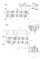
熱伝導性シート1(CNT接合シートの一例)は、図1Aに示すように、固定シート2と、2つのカーボンナノチューブアレイシート3(以下、CNTアレイシート3とする。)とを備えている。
次に、熱伝導性シート1(CNT接合シートの一例)の製造方法の一実施形態について説明する。
このような熱伝導性シート1は、TIMとして、図1Bに示すように、例えば、電子部品11(対象物)と、放熱部材10(対象物)との間に、厚み方向に挟まれるように配置されて使用される。
熱伝導性シート1は、図1Bに示すように、CNTアレイシート3を備えている。そのため、熱伝導性シート1を対象物(例えば、放熱部材10および電子部品11)に接触させたときに、CNTアレイシート3の複数のCNT6を対象物表面の微細な凹凸に追従させることができる。
第1実施形態では、図4Cに示すように、無機物の焼結体4から形成される固定シート2を準備し、その固定シート2にCNTアレイシート3を配置した後、焼成して熱伝導性シート1を製造するが、本発明は、そのような熱伝導性シートの製造方法に限定されない。
次に、図5Bおよび図5Cを参照して、第3実施形態について説明する。なお、上記した第1実施形態および第2実施形態と同様の部材には同様の符号を付し、その説明を省略する。
第1実施形態および第2実施形態では、熱伝導性シート1は、固定シート2の表面2Aおよび裏面2Bの両面に接合されるCNTアレイシート3を備えているが、これに限定されない。図6に示すように、熱伝導性シート1は、固定シート2の表面2Aおよび裏面2Bの少なくともいずれか一方において、固定シート2の焼結体4と接合するCNTアレイシート3を備えていればよい。
ステンレス製の成長基板(ステンレス基板)の表面に二酸化ケイ素膜を積層した後、二酸化ケイ素膜上に、触媒層として鉄を蒸着した。
PVAから形成され、ケイ素粒子(無機粒子)が分散されている樹脂シートを準備した。なお、ケイ素粒子の平均一次粒子径は、2μmであり、ケイ素粒子の含有割合は、樹脂シート全量に対して、20質量%であった。また、PVAの含有割合は、樹脂シート全量に対して、80質量%であった。
PVAが水(溶媒)に溶解されたPVA溶液(樹脂溶液、PVA濃度:10質量%)に、ケイ素粒子(無機粒子)を分散させて、ペーストを準備した。
PVAから形成され、窒化ケイ素粒子(無機粒子)が分散されている樹脂シートを準備したこと以外は、実施例2と同様にして、熱伝導性シートを得た。なお、熱伝導性シートの固定シートの厚みは、100μmであった。
ステンレス製の成長基板の表面および裏面の両面に、二酸化ケイ素膜を積層した後、二酸化ケイ素膜上に、触媒層として鉄を蒸着した。
(1)熱伝導率
各実施例および比較例で得られた熱伝導性シートについて、熱抵抗を熱抵抗測定装置(商品名:T3Ster DynTIM Tester、メンターグラフィックス社製)により測定した。そして、熱伝導性シートの厚みを変更して、熱抵抗を複数点(例えば、3点)測定し、熱伝導性シートの厚みおよび測定された熱抵抗をプロットした。そのプロット結果から、熱伝導性シートの熱伝導率を算出した。その結果を表1に示す。
(2)電気抵抗
各実施例および比較例で得られた熱伝導性シートについて、厚み方向の電気抵抗を電気抵抗測定装置(商品名:レジスティビティ・チェンバ、エーディーシー社製)により測定した。その結果を、表1に示す。
(3)接着強度試験
各実施例で得られた熱伝導性シートについて、粘着テープを、CNTアレイシートに対して、固定シートと反対側から貼着した後、粘着テープを剥離した。
×:CNTアレイシート(VACNTs)の固定シート(成長基板)からの顕著な剥離がみられた。

2 固定シート
3 CNTアレイシート
4 焼結体
6 CNT
7 樹脂シート
8 無機粒子
15 成長基板
19 VACNTs
Claims (7)
- 無機物の焼結体から形成される固定シートと、
前記固定シートの前記焼結体と接合しているカーボンナノチューブアレイシートと、を備えていることを特徴とする、カーボンナノチューブ接合シート。 - 前記無機物は、ケイ素および/またはチタンを含み、
前記焼結体は、前記カーボンナノチューブアレイシートが有する炭素と、前記固定シートに含まれるケイ素および/またはチタンとの焼結体を含んでいることを特徴とする、請求項1に記載のカーボンナノチューブ接合シート。 - 前記カーボンナノチューブアレイシートの前記焼結体と接合する端部は、前記焼結体に埋め込まれていることを特徴とする、請求項1に記載のカーボンナノチューブ接合シート。
- 前記カーボンナノチューブアレイシートの平均嵩密度は、50mg/cm3以上であることを特徴とする、請求項1に記載のカーボンナノチューブ接合シート。
- 無機物の焼結体から形成される固定シートを準備する工程と、
成長基板上に垂直配向カーボンナノチューブを成長させる工程と、
前記成長基板から前記垂直配向カーボンナノチューブを剥離し、カーボンナノチューブアレイシートとする工程と、
前記カーボンナノチューブアレイシートと前記固定シートとの間に金属薄膜を配置する工程と、
前記金属薄膜が配置された前記カーボンナノチューブアレイシートおよび前記固定シートを、真空下または不活性雰囲気下で焼成する工程と、を含むことを特徴とする、カーボンナノチューブ接合シートの製造方法。 - 無機粒子を含有する樹脂シートを準備する工程と、
成長基板上に垂直配向カーボンナノチューブを成長させる工程と、
前記成長基板から前記垂直配向カーボンナノチューブを剥離し、カーボンナノチューブアレイシートとする工程と、
前記カーボンナノチューブアレイシートを前記樹脂シート上に配置する工程と、
前記カーボンナノチューブアレイシートが配置された前記樹脂シートを、真空下または不活性雰囲気下で焼成する工程と、を含むことを特徴とする、カーボンナノチューブ接合シートの製造方法。 - 成長基板上に垂直配向カーボンナノチューブを成長させる工程と、
前記成長基板から前記垂直配向カーボンナノチューブを剥離し、カーボンナノチューブアレイシートとする工程と、
前記カーボンナノチューブアレイシートに、無機粒子を含有するペーストを塗布する工程と、
前記ペーストが塗布されたカーボンナノチューブアレイシートを、真空下または不活性雰囲気下で焼成する工程と、を含むことを特徴とする、カーボンナノチューブ接合シートの製造方法。
Applications Claiming Priority (3)
| Application Number | Priority Date | Filing Date | Title |
|---|---|---|---|
| JP2015256721 | 2015-12-28 | ||
| JP2015256721 | 2015-12-28 | ||
| PCT/JP2016/089030 WO2017115831A1 (ja) | 2015-12-28 | 2016-12-28 | カーボンナノチューブ接合シートおよびカーボンナノチューブ接合シートの製造方法 |
Publications (2)
| Publication Number | Publication Date |
|---|---|
| JPWO2017115831A1 JPWO2017115831A1 (ja) | 2018-11-29 |
| JP6714616B2 true JP6714616B2 (ja) | 2020-06-24 |
Family
ID=59224784
Family Applications (1)
| Application Number | Title | Priority Date | Filing Date |
|---|---|---|---|
| JP2017559229A Active JP6714616B2 (ja) | 2015-12-28 | 2016-12-28 | カーボンナノチューブ接合シートおよびカーボンナノチューブ接合シートの製造方法 |
Country Status (7)
| Country | Link |
|---|---|
| US (1) | US20190010376A1 (ja) |
| EP (1) | EP3398906A4 (ja) |
| JP (1) | JP6714616B2 (ja) |
| KR (1) | KR20180098560A (ja) |
| CN (1) | CN108430919B (ja) |
| TW (1) | TWI725099B (ja) |
| WO (1) | WO2017115831A1 (ja) |
Families Citing this family (7)
| Publication number | Priority date | Publication date | Assignee | Title |
|---|---|---|---|---|
| JP7238586B2 (ja) | 2019-05-08 | 2023-03-14 | 富士通株式会社 | 導電性放熱フィルム、導電性放熱フィルムの製造方法、及び電子装置の製造方法 |
| CN110306167B (zh) * | 2019-06-06 | 2021-06-04 | 沈阳航空航天大学 | 一种原位生长cnt层增强轻质合金胶接界面强度的方法 |
| JP7372092B2 (ja) * | 2019-09-18 | 2023-10-31 | 日立造船株式会社 | カーボンナノチューブ撚糸の製造方法 |
| US11581236B2 (en) * | 2020-02-14 | 2023-02-14 | Micron Technology, Inc. | Self-cleaning heatsink for electronic components |
| CN214176013U (zh) | 2020-12-23 | 2021-09-10 | 迪科特测试科技(苏州)有限公司 | 半导体结构 |
| KR102283073B1 (ko) * | 2021-01-08 | 2021-07-28 | 새빛이앤엘 (주) | 탄성 인터레이어와 cnt 레이어를 이용한 하이브리드 방열 조립체 및 그 조립 방법 |
| US11653475B2 (en) * | 2021-02-01 | 2023-05-16 | Microsoft Technology Licensing, Llc | Thermally conductive microtubes for evenly distributing heat flux on a cooling system |
Family Cites Families (22)
| Publication number | Priority date | Publication date | Assignee | Title |
|---|---|---|---|---|
| FR2856939B1 (fr) * | 2003-07-03 | 2005-09-30 | Jobin Yvon Sas | Humidificateur de gaz |
| US20050116336A1 (en) * | 2003-09-16 | 2005-06-02 | Koila, Inc. | Nano-composite materials for thermal management applications |
| CN100454526C (zh) * | 2005-06-30 | 2009-01-21 | 鸿富锦精密工业(深圳)有限公司 | 热界面材料制造方法 |
| JP5364978B2 (ja) * | 2007-03-28 | 2013-12-11 | 富士通セミコンダクター株式会社 | 表面改質カーボンナノチューブ系材料、その製造方法、電子部材および電子装置 |
| CN100569509C (zh) * | 2007-06-15 | 2009-12-16 | 清华大学 | 一种碳纳米管阵列/层状材料复合物及其制备方法 |
| JP5146371B2 (ja) * | 2008-07-11 | 2013-02-20 | 株式会社豊田中央研究所 | カーボンナノ複合体、それを含む分散液及び樹脂組成物、並びにカーボンナノ複合体の製造方法 |
| JP5463674B2 (ja) * | 2009-01-28 | 2014-04-09 | 株式会社豊田中央研究所 | カーボンナノ複合体、それを含む分散液および樹脂組成物、ならびにカーボンナノ複合体の製造方法 |
| GB0914816D0 (en) * | 2009-08-25 | 2009-09-30 | Isis Innovation | Method of fabrication of aligned nanotube-containing composites |
| JP5293561B2 (ja) * | 2009-10-29 | 2013-09-18 | 富士通株式会社 | 熱伝導性シート及び電子機器 |
| WO2011111112A1 (ja) * | 2010-03-12 | 2011-09-15 | 富士通株式会社 | 放熱構造体およびその製造方法 |
| US9096784B2 (en) * | 2010-07-23 | 2015-08-04 | International Business Machines Corporation | Method and system for allignment of graphite nanofibers for enhanced thermal interface material performance |
| JP2014002273A (ja) * | 2012-06-19 | 2014-01-09 | Nec Corp | 情報表示装置、その制御方法及びプログラム |
| US9656246B2 (en) * | 2012-07-11 | 2017-05-23 | Carbice Corporation | Vertically aligned arrays of carbon nanotubes formed on multilayer substrates |
| JP2014094856A (ja) * | 2012-11-09 | 2014-05-22 | Hitachi Zosen Corp | カーボンナノチューブ生成用基板の製造方法および連続製造装置 |
| JP2014227331A (ja) * | 2013-05-27 | 2014-12-08 | 日立造船株式会社 | カーボンナノチューブシートおよびその製造方法 |
| JP2014234339A (ja) * | 2013-06-05 | 2014-12-15 | 日立造船株式会社 | カーボンナノチューブシートおよびカーボンナノチューブシートの製造方法 |
| JP2015001180A (ja) * | 2013-06-14 | 2015-01-05 | 株式会社東芝 | 軸流タービン |
| JP6186933B2 (ja) * | 2013-06-21 | 2017-08-30 | 富士通株式会社 | 接合シート及びその製造方法、並びに放熱機構及びその製造方法 |
| CN103367275B (zh) | 2013-07-10 | 2016-10-05 | 华为技术有限公司 | 一种界面导热片及其制备方法、散热系统 |
| JP6057877B2 (ja) * | 2013-11-20 | 2017-01-11 | 日立造船株式会社 | カーボンナノチューブシートの製造方法 |
| CN104973583B (zh) * | 2014-04-14 | 2017-04-05 | 清华大学 | 碳纳米管阵列的转移方法及碳纳米管结构的制备方法 |
| CN104973584B (zh) * | 2014-04-14 | 2018-03-02 | 清华大学 | 碳纳米管阵列的转移方法及碳纳米管结构的制备方法 |
-
2016
- 2016-12-28 KR KR1020187018111A patent/KR20180098560A/ko not_active Application Discontinuation
- 2016-12-28 JP JP2017559229A patent/JP6714616B2/ja active Active
- 2016-12-28 WO PCT/JP2016/089030 patent/WO2017115831A1/ja active Application Filing
- 2016-12-28 US US16/066,519 patent/US20190010376A1/en not_active Abandoned
- 2016-12-28 CN CN201680074758.7A patent/CN108430919B/zh active Active
- 2016-12-28 TW TW105143733A patent/TWI725099B/zh active
- 2016-12-28 EP EP16881805.2A patent/EP3398906A4/en not_active Withdrawn
Also Published As
| Publication number | Publication date |
|---|---|
| CN108430919A (zh) | 2018-08-21 |
| KR20180098560A (ko) | 2018-09-04 |
| CN108430919B (zh) | 2022-01-28 |
| TW201722845A (zh) | 2017-07-01 |
| EP3398906A1 (en) | 2018-11-07 |
| EP3398906A4 (en) | 2019-10-23 |
| WO2017115831A1 (ja) | 2017-07-06 |
| JPWO2017115831A1 (ja) | 2018-11-29 |
| US20190010376A1 (en) | 2019-01-10 |
| TWI725099B (zh) | 2021-04-21 |
Similar Documents
| Publication | Publication Date | Title |
|---|---|---|
| JP6714616B2 (ja) | カーボンナノチューブ接合シートおよびカーボンナノチューブ接合シートの製造方法 | |
| US11414321B2 (en) | Carbon nanotube composite material and method for producing carbon nanotube composite material | |
| JP6840725B2 (ja) | カーボンナノチューブ構造体の起毛方法、カーボンナノチューブ構造体の製造方法およびカーボンナノチューブ構造体 | |
| KR102047410B1 (ko) | 접착제 및 하나 또는 그 이상의 나노섬유 시트를 포함하는 다중층 복합재 | |
| US9284196B2 (en) | Graphene-like nanosheet structure network on a substrate and the method for forming the same | |
| US7150911B2 (en) | Electrical insulating vapor grown carbon fiber and method for producing the same, and use thereof | |
| WO2011027756A1 (ja) | 炭化ケイ素被覆炭素基材の製造方法及び炭化ケイ素被覆炭素基材並びに炭化ケイ素炭素複合焼結体、セラミックス被覆炭化ケイ素炭素複合焼結体及び炭化ケイ素炭素複合焼結体の製造方法 | |
| TWI732750B (zh) | 碳奈米管高密度集合體的製造方法 | |
| JPWO2016136826A1 (ja) | カーボンナノチューブ高密度集合体およびカーボンナノチューブ高密度集合体の製造方法 | |
| JP6917725B2 (ja) | カーボンナノチューブ複合材の製造方法、カーボンナノチューブ複合材および異方性カーボンナノチューブ複合材 | |
| JP2010040883A (ja) | 放熱シート、放熱装置、及び放熱シートの製造方法 | |
| KR20170046537A (ko) | 탄소 복합체 및 이를 포함하는 전기 저장 장치 | |
| JP2017071528A (ja) | 層間熱接合材料およびパワー半導体用冷却システム | |
| Meysami et al. | Ultra-stiff large-area carpets of carbon nanotubes | |
| JP2010118502A (ja) | 放熱構造 | |
| JP4827616B2 (ja) | ダイヤモンドの製造方法 | |
| EP3532539A1 (en) | Composite material and method of forming same, and electrical component including composite material | |
| JP7364375B2 (ja) | 炭素複合部材 | |
| JP2024048872A (ja) | 断熱材 | |
| JPWO2014081005A1 (ja) | セラミックス炭素複合材の特性制御方法並びにセラミックス炭素複合材 | |
| RU2007112860A (ru) | Углеродсодержащий наноматериал с низким порогом полевой эмиссии электронов и способ его получения (варианты) | |
| KR20170046536A (ko) | 탄화규소 복합체 및 이를 포함하는 전기 저장 장치 | |
| JP2010159176A (ja) | 放熱シートの製造方法 |
Legal Events
| Date | Code | Title | Description |
|---|---|---|---|
| AA64 | Notification of invalidation of claim of internal priority (with term) |
Free format text: JAPANESE INTERMEDIATE CODE: A241764 Effective date: 20180911 |
|
| A521 | Request for written amendment filed |
Free format text: JAPANESE INTERMEDIATE CODE: A523 Effective date: 20180912 |
|
| A521 | Request for written amendment filed |
Free format text: JAPANESE INTERMEDIATE CODE: A821 Effective date: 20180912 |
|
| A621 | Written request for application examination |
Free format text: JAPANESE INTERMEDIATE CODE: A621 Effective date: 20190415 |
|
| TRDD | Decision of grant or rejection written | ||
| A01 | Written decision to grant a patent or to grant a registration (utility model) |
Free format text: JAPANESE INTERMEDIATE CODE: A01 Effective date: 20200519 |
|
| A61 | First payment of annual fees (during grant procedure) |
Free format text: JAPANESE INTERMEDIATE CODE: A61 Effective date: 20200605 |
|
| R150 | Certificate of patent or registration of utility model |
Ref document number: 6714616 Country of ref document: JP Free format text: JAPANESE INTERMEDIATE CODE: R150 |
|
| R250 | Receipt of annual fees |
Free format text: JAPANESE INTERMEDIATE CODE: R250 |