JP6714616B2 - Carbon nanotube bonding sheet and method for manufacturing carbon nanotube bonding sheet - Google Patents
Carbon nanotube bonding sheet and method for manufacturing carbon nanotube bonding sheet Download PDFInfo
- Publication number
- JP6714616B2 JP6714616B2 JP2017559229A JP2017559229A JP6714616B2 JP 6714616 B2 JP6714616 B2 JP 6714616B2 JP 2017559229 A JP2017559229 A JP 2017559229A JP 2017559229 A JP2017559229 A JP 2017559229A JP 6714616 B2 JP6714616 B2 JP 6714616B2
- Authority
- JP
- Japan
- Prior art keywords
- sheet
- carbon nanotube
- array sheet
- cnt array
- sintered body
- Prior art date
- Legal status (The legal status is an assumption and is not a legal conclusion. Google has not performed a legal analysis and makes no representation as to the accuracy of the status listed.)
- Active
Links
Images


Classifications
-
- B—PERFORMING OPERATIONS; TRANSPORTING
- B32—LAYERED PRODUCTS
- B32B—LAYERED PRODUCTS, i.e. PRODUCTS BUILT-UP OF STRATA OF FLAT OR NON-FLAT, e.g. CELLULAR OR HONEYCOMB, FORM
- B32B9/00—Layered products comprising a layer of a particular substance not covered by groups B32B11/00 - B32B29/00
- B32B9/005—Layered products comprising a layer of a particular substance not covered by groups B32B11/00 - B32B29/00 comprising one layer of ceramic material, e.g. porcelain, ceramic tile
- B32B9/007—Layered products comprising a layer of a particular substance not covered by groups B32B11/00 - B32B29/00 comprising one layer of ceramic material, e.g. porcelain, ceramic tile comprising carbon, e.g. graphite, composite carbon
-
- B—PERFORMING OPERATIONS; TRANSPORTING
- B22—CASTING; POWDER METALLURGY
- B22F—WORKING METALLIC POWDER; MANUFACTURE OF ARTICLES FROM METALLIC POWDER; MAKING METALLIC POWDER; APPARATUS OR DEVICES SPECIALLY ADAPTED FOR METALLIC POWDER
- B22F7/00—Manufacture of composite layers, workpieces, or articles, comprising metallic powder, by sintering the powder, with or without compacting wherein at least one part is obtained by sintering or compression
- B22F7/06—Manufacture of composite layers, workpieces, or articles, comprising metallic powder, by sintering the powder, with or without compacting wherein at least one part is obtained by sintering or compression of composite workpieces or articles from parts, e.g. to form tipped tools
- B22F7/08—Manufacture of composite layers, workpieces, or articles, comprising metallic powder, by sintering the powder, with or without compacting wherein at least one part is obtained by sintering or compression of composite workpieces or articles from parts, e.g. to form tipped tools with one or more parts not made from powder
-
- B—PERFORMING OPERATIONS; TRANSPORTING
- B28—WORKING CEMENT, CLAY, OR STONE
- B28B—SHAPING CLAY OR OTHER CERAMIC COMPOSITIONS; SHAPING SLAG; SHAPING MIXTURES CONTAINING CEMENTITIOUS MATERIAL, e.g. PLASTER
- B28B11/00—Apparatus or processes for treating or working the shaped or preshaped articles
- B28B11/24—Apparatus or processes for treating or working the shaped or preshaped articles for curing, setting or hardening
- B28B11/243—Setting, e.g. drying, dehydrating or firing ceramic articles
-
- B—PERFORMING OPERATIONS; TRANSPORTING
- B32—LAYERED PRODUCTS
- B32B—LAYERED PRODUCTS, i.e. PRODUCTS BUILT-UP OF STRATA OF FLAT OR NON-FLAT, e.g. CELLULAR OR HONEYCOMB, FORM
- B32B15/00—Layered products comprising a layer of metal
- B32B15/04—Layered products comprising a layer of metal comprising metal as the main or only constituent of a layer, which is next to another layer of the same or of a different material
-
- B—PERFORMING OPERATIONS; TRANSPORTING
- B32—LAYERED PRODUCTS
- B32B—LAYERED PRODUCTS, i.e. PRODUCTS BUILT-UP OF STRATA OF FLAT OR NON-FLAT, e.g. CELLULAR OR HONEYCOMB, FORM
- B32B38/00—Ancillary operations in connection with laminating processes
- B32B38/0036—Heat treatment
-
- B—PERFORMING OPERATIONS; TRANSPORTING
- B32—LAYERED PRODUCTS
- B32B—LAYERED PRODUCTS, i.e. PRODUCTS BUILT-UP OF STRATA OF FLAT OR NON-FLAT, e.g. CELLULAR OR HONEYCOMB, FORM
- B32B5/00—Layered products characterised by the non- homogeneity or physical structure, i.e. comprising a fibrous, filamentary, particulate or foam layer; Layered products characterised by having a layer differing constitutionally or physically in different parts
- B32B5/02—Layered products characterised by the non- homogeneity or physical structure, i.e. comprising a fibrous, filamentary, particulate or foam layer; Layered products characterised by having a layer differing constitutionally or physically in different parts characterised by structural features of a fibrous or filamentary layer
-
- B—PERFORMING OPERATIONS; TRANSPORTING
- B32—LAYERED PRODUCTS
- B32B—LAYERED PRODUCTS, i.e. PRODUCTS BUILT-UP OF STRATA OF FLAT OR NON-FLAT, e.g. CELLULAR OR HONEYCOMB, FORM
- B32B9/00—Layered products comprising a layer of a particular substance not covered by groups B32B11/00 - B32B29/00
-
- B—PERFORMING OPERATIONS; TRANSPORTING
- B82—NANOTECHNOLOGY
- B82Y—SPECIFIC USES OR APPLICATIONS OF NANOSTRUCTURES; MEASUREMENT OR ANALYSIS OF NANOSTRUCTURES; MANUFACTURE OR TREATMENT OF NANOSTRUCTURES
- B82Y40/00—Manufacture or treatment of nanostructures
-
- C—CHEMISTRY; METALLURGY
- C01—INORGANIC CHEMISTRY
- C01B—NON-METALLIC ELEMENTS; COMPOUNDS THEREOF; METALLOIDS OR COMPOUNDS THEREOF NOT COVERED BY SUBCLASS C01C
- C01B32/00—Carbon; Compounds thereof
- C01B32/15—Nano-sized carbon materials
- C01B32/158—Carbon nanotubes
- C01B32/168—After-treatment
-
- C—CHEMISTRY; METALLURGY
- C09—DYES; PAINTS; POLISHES; NATURAL RESINS; ADHESIVES; COMPOSITIONS NOT OTHERWISE PROVIDED FOR; APPLICATIONS OF MATERIALS NOT OTHERWISE PROVIDED FOR
- C09K—MATERIALS FOR MISCELLANEOUS APPLICATIONS, NOT PROVIDED FOR ELSEWHERE
- C09K5/00—Heat-transfer, heat-exchange or heat-storage materials, e.g. refrigerants; Materials for the production of heat or cold by chemical reactions other than by combustion
- C09K5/08—Materials not undergoing a change of physical state when used
- C09K5/14—Solid materials, e.g. powdery or granular
-
- C—CHEMISTRY; METALLURGY
- C23—COATING METALLIC MATERIAL; COATING MATERIAL WITH METALLIC MATERIAL; CHEMICAL SURFACE TREATMENT; DIFFUSION TREATMENT OF METALLIC MATERIAL; COATING BY VACUUM EVAPORATION, BY SPUTTERING, BY ION IMPLANTATION OR BY CHEMICAL VAPOUR DEPOSITION, IN GENERAL; INHIBITING CORROSION OF METALLIC MATERIAL OR INCRUSTATION IN GENERAL
- C23C—COATING METALLIC MATERIAL; COATING MATERIAL WITH METALLIC MATERIAL; SURFACE TREATMENT OF METALLIC MATERIAL BY DIFFUSION INTO THE SURFACE, BY CHEMICAL CONVERSION OR SUBSTITUTION; COATING BY VACUUM EVAPORATION, BY SPUTTERING, BY ION IMPLANTATION OR BY CHEMICAL VAPOUR DEPOSITION, IN GENERAL
- C23C16/00—Chemical coating by decomposition of gaseous compounds, without leaving reaction products of surface material in the coating, i.e. chemical vapour deposition [CVD] processes
- C23C16/22—Chemical coating by decomposition of gaseous compounds, without leaving reaction products of surface material in the coating, i.e. chemical vapour deposition [CVD] processes characterised by the deposition of inorganic material, other than metallic material
- C23C16/26—Deposition of carbon only
-
- H—ELECTRICITY
- H01—ELECTRIC ELEMENTS
- H01L—SEMICONDUCTOR DEVICES NOT COVERED BY CLASS H10
- H01L23/00—Details of semiconductor or other solid state devices
- H01L23/34—Arrangements for cooling, heating, ventilating or temperature compensation ; Temperature sensing arrangements
- H01L23/36—Selection of materials, or shaping, to facilitate cooling or heating, e.g. heatsinks
- H01L23/373—Cooling facilitated by selection of materials for the device or materials for thermal expansion adaptation, e.g. carbon
-
- H—ELECTRICITY
- H01—ELECTRIC ELEMENTS
- H01L—SEMICONDUCTOR DEVICES NOT COVERED BY CLASS H10
- H01L24/00—Arrangements for connecting or disconnecting semiconductor or solid-state bodies; Methods or apparatus related thereto
- H01L24/01—Means for bonding being attached to, or being formed on, the surface to be connected, e.g. chip-to-package, die-attach, "first-level" interconnects; Manufacturing methods related thereto
- H01L24/26—Layer connectors, e.g. plate connectors, solder or adhesive layers; Manufacturing methods related thereto
- H01L24/27—Manufacturing methods
-
- H—ELECTRICITY
- H01—ELECTRIC ELEMENTS
- H01L—SEMICONDUCTOR DEVICES NOT COVERED BY CLASS H10
- H01L24/00—Arrangements for connecting or disconnecting semiconductor or solid-state bodies; Methods or apparatus related thereto
- H01L24/01—Means for bonding being attached to, or being formed on, the surface to be connected, e.g. chip-to-package, die-attach, "first-level" interconnects; Manufacturing methods related thereto
- H01L24/26—Layer connectors, e.g. plate connectors, solder or adhesive layers; Manufacturing methods related thereto
- H01L24/28—Structure, shape, material or disposition of the layer connectors prior to the connecting process
- H01L24/29—Structure, shape, material or disposition of the layer connectors prior to the connecting process of an individual layer connector
-
- H—ELECTRICITY
- H05—ELECTRIC TECHNIQUES NOT OTHERWISE PROVIDED FOR
- H05K—PRINTED CIRCUITS; CASINGS OR CONSTRUCTIONAL DETAILS OF ELECTRIC APPARATUS; MANUFACTURE OF ASSEMBLAGES OF ELECTRICAL COMPONENTS
- H05K7/00—Constructional details common to different types of electric apparatus
- H05K7/20—Modifications to facilitate cooling, ventilating, or heating
-
- B—PERFORMING OPERATIONS; TRANSPORTING
- B32—LAYERED PRODUCTS
- B32B—LAYERED PRODUCTS, i.e. PRODUCTS BUILT-UP OF STRATA OF FLAT OR NON-FLAT, e.g. CELLULAR OR HONEYCOMB, FORM
- B32B2305/00—Condition, form or state of the layers or laminate
- B32B2305/80—Sintered
-
- B—PERFORMING OPERATIONS; TRANSPORTING
- B82—NANOTECHNOLOGY
- B82Y—SPECIFIC USES OR APPLICATIONS OF NANOSTRUCTURES; MEASUREMENT OR ANALYSIS OF NANOSTRUCTURES; MANUFACTURE OR TREATMENT OF NANOSTRUCTURES
- B82Y30/00—Nanotechnology for materials or surface science, e.g. nanocomposites
-
- C—CHEMISTRY; METALLURGY
- C01—INORGANIC CHEMISTRY
- C01B—NON-METALLIC ELEMENTS; COMPOUNDS THEREOF; METALLOIDS OR COMPOUNDS THEREOF NOT COVERED BY SUBCLASS C01C
- C01B2202/00—Structure or properties of carbon nanotubes
- C01B2202/20—Nanotubes characterized by their properties
- C01B2202/24—Thermal properties
-
- H—ELECTRICITY
- H01—ELECTRIC ELEMENTS
- H01L—SEMICONDUCTOR DEVICES NOT COVERED BY CLASS H10
- H01L2224/00—Indexing scheme for arrangements for connecting or disconnecting semiconductor or solid-state bodies and methods related thereto as covered by H01L24/00
- H01L2224/01—Means for bonding being attached to, or being formed on, the surface to be connected, e.g. chip-to-package, die-attach, "first-level" interconnects; Manufacturing methods related thereto
- H01L2224/26—Layer connectors, e.g. plate connectors, solder or adhesive layers; Manufacturing methods related thereto
- H01L2224/27—Manufacturing methods
- H01L2224/27001—Involving a temporary auxiliary member not forming part of the manufacturing apparatus, e.g. removable or sacrificial coating, film or substrate
- H01L2224/27003—Involving a temporary auxiliary member not forming part of the manufacturing apparatus, e.g. removable or sacrificial coating, film or substrate for holding or transferring the layer preform
-
- H—ELECTRICITY
- H01—ELECTRIC ELEMENTS
- H01L—SEMICONDUCTOR DEVICES NOT COVERED BY CLASS H10
- H01L2224/00—Indexing scheme for arrangements for connecting or disconnecting semiconductor or solid-state bodies and methods related thereto as covered by H01L24/00
- H01L2224/01—Means for bonding being attached to, or being formed on, the surface to be connected, e.g. chip-to-package, die-attach, "first-level" interconnects; Manufacturing methods related thereto
- H01L2224/26—Layer connectors, e.g. plate connectors, solder or adhesive layers; Manufacturing methods related thereto
- H01L2224/27—Manufacturing methods
- H01L2224/275—Manufacturing methods by chemical or physical modification of a pre-existing or pre-deposited material
- H01L2224/27505—Sintering
-
- H—ELECTRICITY
- H01—ELECTRIC ELEMENTS
- H01L—SEMICONDUCTOR DEVICES NOT COVERED BY CLASS H10
- H01L2224/00—Indexing scheme for arrangements for connecting or disconnecting semiconductor or solid-state bodies and methods related thereto as covered by H01L24/00
- H01L2224/01—Means for bonding being attached to, or being formed on, the surface to be connected, e.g. chip-to-package, die-attach, "first-level" interconnects; Manufacturing methods related thereto
- H01L2224/26—Layer connectors, e.g. plate connectors, solder or adhesive layers; Manufacturing methods related thereto
- H01L2224/28—Structure, shape, material or disposition of the layer connectors prior to the connecting process
- H01L2224/29—Structure, shape, material or disposition of the layer connectors prior to the connecting process of an individual layer connector
- H01L2224/29001—Core members of the layer connector
- H01L2224/29099—Material
- H01L2224/291—Material with a principal constituent of the material being a metal or a metalloid, e.g. boron [B], silicon [Si], germanium [Ge], arsenic [As], antimony [Sb], tellurium [Te] and polonium [Po], and alloys thereof
- H01L2224/29138—Material with a principal constituent of the material being a metal or a metalloid, e.g. boron [B], silicon [Si], germanium [Ge], arsenic [As], antimony [Sb], tellurium [Te] and polonium [Po], and alloys thereof the principal constituent melting at a temperature of greater than or equal to 950°C and less than 1550°C
-
- H—ELECTRICITY
- H01—ELECTRIC ELEMENTS
- H01L—SEMICONDUCTOR DEVICES NOT COVERED BY CLASS H10
- H01L2224/00—Indexing scheme for arrangements for connecting or disconnecting semiconductor or solid-state bodies and methods related thereto as covered by H01L24/00
- H01L2224/01—Means for bonding being attached to, or being formed on, the surface to be connected, e.g. chip-to-package, die-attach, "first-level" interconnects; Manufacturing methods related thereto
- H01L2224/26—Layer connectors, e.g. plate connectors, solder or adhesive layers; Manufacturing methods related thereto
- H01L2224/28—Structure, shape, material or disposition of the layer connectors prior to the connecting process
- H01L2224/29—Structure, shape, material or disposition of the layer connectors prior to the connecting process of an individual layer connector
- H01L2224/29001—Core members of the layer connector
- H01L2224/29099—Material
- H01L2224/291—Material with a principal constituent of the material being a metal or a metalloid, e.g. boron [B], silicon [Si], germanium [Ge], arsenic [As], antimony [Sb], tellurium [Te] and polonium [Po], and alloys thereof
- H01L2224/29163—Material with a principal constituent of the material being a metal or a metalloid, e.g. boron [B], silicon [Si], germanium [Ge], arsenic [As], antimony [Sb], tellurium [Te] and polonium [Po], and alloys thereof the principal constituent melting at a temperature of greater than 1550°C
- H01L2224/29166—Titanium [Ti] as principal constituent
-
- H—ELECTRICITY
- H01—ELECTRIC ELEMENTS
- H01L—SEMICONDUCTOR DEVICES NOT COVERED BY CLASS H10
- H01L2224/00—Indexing scheme for arrangements for connecting or disconnecting semiconductor or solid-state bodies and methods related thereto as covered by H01L24/00
- H01L2224/01—Means for bonding being attached to, or being formed on, the surface to be connected, e.g. chip-to-package, die-attach, "first-level" interconnects; Manufacturing methods related thereto
- H01L2224/26—Layer connectors, e.g. plate connectors, solder or adhesive layers; Manufacturing methods related thereto
- H01L2224/28—Structure, shape, material or disposition of the layer connectors prior to the connecting process
- H01L2224/29—Structure, shape, material or disposition of the layer connectors prior to the connecting process of an individual layer connector
- H01L2224/29001—Core members of the layer connector
- H01L2224/29099—Material
- H01L2224/29193—Material with a principal constituent of the material being a solid not provided for in groups H01L2224/291 - H01L2224/29191, e.g. allotropes of carbon, fullerene, graphite, carbon-nanotubes, diamond
-
- H—ELECTRICITY
- H01—ELECTRIC ELEMENTS
- H01L—SEMICONDUCTOR DEVICES NOT COVERED BY CLASS H10
- H01L2924/00—Indexing scheme for arrangements or methods for connecting or disconnecting semiconductor or solid-state bodies as covered by H01L24/00
- H01L2924/01—Chemical elements
- H01L2924/01014—Silicon [Si]
Description
本発明は、カーボンナノチューブ接合シートおよびカーボンナノチューブ接合シートの製造方法に関する。 The present invention relates to a carbon nanotube-bonded sheet and a method for manufacturing a carbon nanotube-bonded sheet.
電子部品とヒートシンクとの間に熱伝導性材料(Thermal Interface Material:以下、TIMとする。)を配置して、電子部品とヒートシンクとの間の隙間を低減して、電子部品から発生する熱を効率よくヒートシンクに伝導することが知られている。このようなTIMとして、高分子材料からなる高分子シートや、シリコーングリースなどが知られている。 A heat conductive material (hereinafter, referred to as TIM) is arranged between the electronic component and the heat sink to reduce a gap between the electronic component and the heat sink to reduce heat generated from the electronic component. It is known to efficiently conduct to a heat sink. As such a TIM, a polymer sheet made of a polymer material and silicone grease are known.
しかし、高分子シートは、電子部品およびヒートシンクの表面の微細な凹凸(表面粗さ)に十分に追従することができず、その微細な凹凸により、電子部品とヒートシンクとの間に空隙が生じる場合があり、熱伝導率の向上を図るには限度がある。 However, the polymer sheet cannot sufficiently follow the fine irregularities (surface roughness) on the surfaces of the electronic component and the heat sink, and when the fine irregularities cause a gap between the electronic component and the heat sink. However, there is a limit to improving the thermal conductivity.
また、シリコーングリースは、電子部品およびヒートシンクの表面の微細な凹凸に追従することができるが、温度変化が繰り返されることにより、ポンプアウト(電子部品とヒートシンクとの間から流出)する場合があり、長期にわたってTIMの熱伝導性能を確保することは困難である。 Further, the silicone grease can follow fine irregularities on the surface of the electronic component and the heat sink, but may be pumped out (flow out from between the electronic component and the heat sink) due to repeated temperature changes. It is difficult to secure the thermal conductivity of TIM for a long period of time.
そこで、電子部品およびヒートシンクの表面の微細な凹凸に追従させることができながら、長期にわたって熱伝導性能を確保できるTIMが望まれており、TIMにカーボンナノチューブ(以下、CNTとする。)を利用することが検討されている。 Therefore, there is a demand for a TIM that can ensure the heat conduction performance for a long period of time while being able to follow fine irregularities on the surfaces of the electronic component and the heat sink, and uses carbon nanotubes (hereinafter referred to as CNTs) for the TIM. Is being considered.
例えば、基板と、基板の両面にアレイ状に配置されるCNTとを備える熱界面パッドが提案されている(例えば、特許文献1参照)。 For example, a thermal interface pad including a substrate and CNTs arranged in an array on both surfaces of the substrate has been proposed (see, for example, Patent Document 1).
そのような熱界面パッドは、CNTを、化学気相蒸着によって、基板の両面に成長させて製造される。そして、そのような熱界面パッドでは、CNTが基板の両面に配置されているので、そのCNTを電子部品およびヒートシンクの表面の微細な凹凸に追従させることができる。 Such thermal interface pads are manufactured by growing CNTs on both sides of a substrate by chemical vapor deposition. Further, in such a thermal interface pad, since the CNTs are arranged on both surfaces of the substrate, the CNTs can be made to follow fine irregularities on the surfaces of the electronic component and the heat sink.
しかし、特許文献1に記載の熱界面パッドは、化学気相蒸着により、CNTを基板の両面に成長させて製造されているので、基板とCNTとの接着強度を十分に確保することができない。そのため、熱界面パッドをTIMとして使用すると、CNTが基板から脱落してしまう場合がある。この場合、熱界面パッドの熱伝導性能を確保することは困難であり、また、脱落したCNTが電子部品などの短絡を引き起こす場合がある。
However, since the thermal interface pad described in
そこで、本発明の目的は、対象物の表面の微細な凹凸に追従させることができながら、カーボンナノチューブが脱落することを抑制できるカーボンナノチューブ接合シートおよびカーボンナノチューブ接合シートの製造方法を提供することにある。 Therefore, an object of the present invention is to provide a carbon nanotube-bonding sheet and a method for manufacturing a carbon nanotube-bonding sheet capable of suppressing the falling of carbon nanotubes while being able to follow fine irregularities on the surface of an object. is there.
本発明[1]は、無機物の焼結体から形成される固定シートと、前記固定シートの前記焼結体と接合しているカーボンナノチューブアレイシートと、を備えている、カーボンナノチューブ接合シートを含んでいる。 The present invention [1] includes a carbon nanotube-bonding sheet including a fixing sheet formed of an inorganic sintered body, and a carbon nanotube array sheet bonded to the sintered body of the fixing sheet. I'm out.
このような構成によれば、カーボンナノチューブ接合シートがカーボンナノチューブアレイシートを備えているので、カーボンナノチューブ接合シートを対象物に接触させたときに、カーボンナノチューブアレイシートの複数のCNTを対象物表面の微細な凹凸に追従させることができる。 According to such a configuration, since the carbon nanotube-bonded sheet includes the carbon nanotube array sheet, when the carbon nanotube-bonded sheet is brought into contact with the object, a plurality of CNTs of the carbon nanotube array sheet are attached to the surface of the object. It is possible to follow fine irregularities.
また、カーボンナノチューブアレイシートが、固定シートの焼結体と接合しているので、カーボンナノチューブアレイシートが有するCNTが、固定シートから脱落することを抑制できる。 Further, since the carbon nanotube array sheet is joined to the sintered body of the fixed sheet, it is possible to prevent the CNTs of the carbon nanotube array sheet from falling off the fixed sheet.
本発明[2]は、前記無機物は、ケイ素および/またはチタンを含み、前記焼結体は、前記カーボンナノチューブアレイシートが有する炭素と、前記固定シートに含まれるケイ素および/またはチタンとの焼結体を含んでいる、上記[1]に記載のカーボンナノチューブ接合シートを含んでいる。 In the present invention [2], the inorganic material contains silicon and/or titanium, and the sintered body is obtained by sintering carbon contained in the carbon nanotube array sheet and silicon and/or titanium contained in the fixed sheet. The carbon nanotube-bonding sheet according to [1] above, which contains a body, is included.
このような構成によれば、焼結体が、カーボンナノチューブアレイシートが有する炭素と、固定シートに含まれるケイ素および/またはチタンとの焼結体を含んでいるので、カーボンナノチューブアレイシートと焼結体との親和性の向上を図ることができ、カーボンナノチューブアレイシートを焼結体に確実に接合することができる。そのため、カーボンナノチューブアレイシートが有するCNTが、固定シートから脱落することを確実に抑制できる。 According to this structure, since the sintered body contains the sintered body of carbon contained in the carbon nanotube array sheet and silicon and/or titanium contained in the fixed sheet, the sintered body is sintered with the carbon nanotube array sheet. The affinity with the body can be improved, and the carbon nanotube array sheet can be reliably bonded to the sintered body. Therefore, it is possible to reliably prevent the CNTs included in the carbon nanotube array sheet from falling off the fixing sheet.
本発明[3]は、カーボンナノチューブアレイシートの前記焼結体と接合する端部は、前記焼結体に埋め込まれている、上記[1]または[2]に記載のカーボンナノチューブ接合シートを含んでいる。 The present invention [3] includes the carbon nanotube bonding sheet according to the above [1] or [2], wherein an end portion of the carbon nanotube array sheet that is bonded to the sintered body is embedded in the sintered body. I'm out.
このような構成によれば、カーボンナノチューブアレイシートの端部が焼結体に埋め込まれているので、カーボンナノチューブアレイシートが有するCNTが、固定シートから脱落することをより一層確実に抑制できる。 According to such a configuration, since the ends of the carbon nanotube array sheet are embedded in the sintered body, it is possible to more reliably prevent the CNTs of the carbon nanotube array sheet from falling off the fixed sheet.
本発明[4]は、前記カーボンナノチューブアレイシートの平均嵩密度は、50mg/cm3以上である、上記[1]〜[3]のいずれか一項に記載のカーボンナノチューブ接合シートを含んでいる。The present invention [4] includes the carbon nanotube bonding sheet according to any one of the above [1] to [3], wherein the carbon nanotube array sheet has an average bulk density of 50 mg/cm 3 or more. ..
このような構成によれば、カーボンナノチューブアレイシートの平均嵩密度が上記下限以上であるので、カーボンナノチューブアレイシートの熱伝導率の向上を図ることができ、ひいては、カーボンナノチューブ接合シートの熱伝導率の向上を図ることができる。 According to such a configuration, since the average bulk density of the carbon nanotube array sheet is not less than the above lower limit, it is possible to improve the thermal conductivity of the carbon nanotube array sheet, and thus the thermal conductivity of the carbon nanotube bonding sheet. Can be improved.
しかるに、カーボンナノチューブアレイを化学気相蒸着により基板の両面に成長させる場合、カーボンナノチューブアレイの平均嵩密度を上記下限以上とすることは困難である。 However, when the carbon nanotube array is grown on both surfaces of the substrate by chemical vapor deposition, it is difficult to set the average bulk density of the carbon nanotube array to the above lower limit or more.
一方、上記の構成によれば、成長基板から剥離されたカーボンナノチューブアレイシートが、固定シートの焼結体と接合しているので、カーボンナノチューブアレイシートを、成長基板から剥離した後、高密度化処理することができる。そのため、カーボンナノチューブアレイシートの平均嵩密度を上記下限以上とすることができる。 On the other hand, according to the above configuration, since the carbon nanotube array sheet peeled from the growth substrate is bonded to the sintered body of the fixed sheet, the carbon nanotube array sheet is densified after being peeled from the growth substrate. Can be processed. Therefore, the average bulk density of the carbon nanotube array sheet can be set to the above lower limit or more.
本発明[5]は、無機物の焼結体から形成される固定シートを準備する工程と、成長基板上に垂直配向カーボンナノチューブを成長させる工程と、前記成長基板から前記垂直配向カーボンナノチューブを剥離し、カーボンナノチューブアレイシートとする工程と、前記カーボンナノチューブアレイシートと前記固定シートとの間に金属薄膜を配置する工程と、前記金属薄膜が配置された前記カーボンナノチューブアレイシートおよび前記固定シートを、真空下または不活性雰囲気下で焼成する工程と、を含む、カーボンナノチューブ接合シートの製造方法を含んでいる。 The present invention [5] provides a step of preparing a fixed sheet formed of an inorganic sintered body, a step of growing vertically aligned carbon nanotubes on a growth substrate, and peeling the vertically aligned carbon nanotubes from the growth substrate. A step of forming a carbon nanotube array sheet, a step of disposing a metal thin film between the carbon nanotube array sheet and the fixing sheet, and a vacuum treatment of the carbon nanotube array sheet and the fixing sheet on which the metal thin film is arranged, And a step of firing under an inert atmosphere.
このような方法によれば、成長基板から剥離したカーボンナノチューブアレイシートと、無機物の焼結体から形成される固定シートとの間に金属薄膜を配置した後、それらを焼成することにより、カーボンナノチューブアレイシートを固定シートと強固に接合させることができる。 According to such a method, a carbon thin film is placed between a carbon nanotube array sheet separated from a growth substrate and a fixed sheet formed of a sintered body of an inorganic material, and then the thin film is fired to form a carbon nanotube. The array sheet can be firmly bonded to the fixed sheet.
そのため、簡易な方法でありながら、固定シートの焼結体と接合するカーボンナノチューブアレイシートを備えるカーボンナノチューブ接合シートを効率良く製造することができる。 Therefore, although it is a simple method, it is possible to efficiently manufacture the carbon nanotube-bonded sheet including the carbon nanotube array sheet that is bonded to the sintered body of the fixed sheet.
本発明[6]は、無機粒子を含有する樹脂シートを準備する工程と、成長基板上に垂直配向カーボンナノチューブを成長させる工程と、前記成長基板から前記垂直配向カーボンナノチューブを剥離し、カーボンナノチューブアレイシートとする工程と、前記カーボンナノチューブアレイシートを前記樹脂シート上に配置する工程と、前記カーボンナノチューブアレイシートが配置された前記樹脂シートを、真空下または不活性雰囲気下で焼成する工程と、を含む、カーボンナノチューブ接合シートの製造方法を含んでいる。 The present invention [6] provides a step of preparing a resin sheet containing inorganic particles, a step of growing vertically aligned carbon nanotubes on a growth substrate, and a step of separating the vertically aligned carbon nanotubes from the growth substrate to form a carbon nanotube array. A step of forming a sheet, a step of disposing the carbon nanotube array sheet on the resin sheet, and a step of firing the resin sheet on which the carbon nanotube array sheet is disposed under a vacuum or an inert atmosphere, Including, the method for manufacturing the carbon nanotube bonding sheet is included.
このような方法によれば、成長基板から剥離したカーボンナノチューブアレイシートを、無機粒子を含有する樹脂シート上に配置した後、焼成することにより、無機粒子を焼結体とすることができ、固定シートを形成できる。そして、カーボンナノチューブアレイシートを固定シートの焼結体と接合させることができる。 According to such a method, the carbon nanotube array sheet separated from the growth substrate is placed on the resin sheet containing the inorganic particles and then fired, whereby the inorganic particles can be made into a sintered body and fixed. Sheets can be formed. Then, the carbon nanotube array sheet can be joined to the sintered body of the fixed sheet.
そのため、簡易な方法でありながら、固定シートの焼結体と接合するカーボンナノチューブアレイシートを備えるカーボンナノチューブ接合シートを効率良く製造することができる。 Therefore, although it is a simple method, it is possible to efficiently manufacture the carbon nanotube-bonded sheet including the carbon nanotube array sheet that is bonded to the sintered body of the fixed sheet.
本発明[7]は、成長基板上に垂直配向カーボンナノチューブを成長させる工程と、前記成長基板から前記垂直配向カーボンナノチューブを剥離し、カーボンナノチューブアレイシートとする工程と、前記カーボンナノチューブアレイシートに、無機粒子を含有するペーストを塗布する工程と、前記ペーストが塗布されたカーボンナノチューブアレイシートを、真空下または不活性雰囲気下で焼成する工程と、を含む、カーボンナノチューブ接合シートの製造方法を含んでいる。 The present invention [7] comprises: a step of growing vertically aligned carbon nanotubes on a growth substrate; a step of peeling the vertically aligned carbon nanotubes from the growth substrate to form a carbon nanotube array sheet; A step of applying a paste containing inorganic particles, a step of firing the carbon nanotube array sheet coated with the paste under vacuum or in an inert atmosphere, including a method for producing a carbon nanotube bonding sheet, There is.
このような方法によれば、成長基板から剥離したカーボンナノチューブアレイシートに、無機粒子を含有するペーストを塗布した後、焼成することにより、無機粒子を焼結体とすることができ、固定シートを形成できる。そして、カーボンナノチューブアレイシートを固定シートの焼結体と接合させることができる。 According to such a method, the carbon nanotube array sheet separated from the growth substrate is coated with the paste containing the inorganic particles and then fired, whereby the inorganic particles can be made into a sintered body, and the fixing sheet is formed. Can be formed. Then, the carbon nanotube array sheet can be joined to the sintered body of the fixed sheet.
そのため、簡易な方法でありながら、固定シートの焼結体と接合するカーボンナノチューブアレイシートを備えるカーボンナノチューブ接合シートを効率良く製造することができる。 Therefore, although it is a simple method, it is possible to efficiently manufacture the carbon nanotube-bonded sheet including the carbon nanotube array sheet that is bonded to the sintered body of the fixed sheet.
本発明のカーボンナノチューブ接合シートは、対象物の表面の微細な凹凸に追従することができながら、CNTが脱落することを抑制できる。 The carbon nanotube-bonded sheet of the present invention can follow fine irregularities on the surface of an object, but can prevent CNT from falling off.
本発明のカーボンナノチューブ接合シートの製造方法は、簡易な方法でありながら、上記のカーボンナノチューブ接合シートを効率良く製造することができる。 The method for producing a carbon nanotube-bonded sheet of the present invention is a simple method, but the above carbon nanotube-bonded sheet can be efficiently produced.
本発明のカーボンナノチューブ接合シート(以下、CNT接合シートとする。)は、無機物の焼結体から形成される固定シートと、固定シートの焼結体と接合しているカーボンナノチューブアレイシートと、を備えている。カーボンナノチューブアレイシートは、固定シートに接合されていればよく、例えば、固定シートの表面および裏面の少なくともいずれか一方に接合されている。 The carbon nanotube bonding sheet (hereinafter, referred to as CNT bonding sheet) of the present invention includes a fixed sheet formed of an inorganic sintered body and a carbon nanotube array sheet bonded to the fixed sheet sintered body. I have it. It suffices that the carbon nanotube array sheet is bonded to the fixed sheet, and for example, it is bonded to at least one of the front surface and the back surface of the fixed sheet.
以下に、本発明のCNT接合シートの第1実施形態としての熱伝導性シート1について説明する。
1.第1実施形態
(1)熱伝導性シートの構成
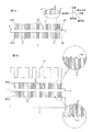
熱伝導性シート1(CNT接合シートの一例)は、図1Aに示すように、固定シート2と、2つのカーボンナノチューブアレイシート3(以下、CNTアレイシート3とする。)とを備えている。Below, the heat
1. First Embodiment (1) Configuration of Heat Conductive Sheet As shown in FIG. 1A, a heat conductive sheet 1 (an example of a CNT bonding sheet) includes a fixing
固定シート2は、シート形状(平板形状)を有しており、具体的には、固定シート2は、所定の厚みを有し、その厚み方向と直交する面方向(縦方向および横方向)に延びており、平坦な表面2A(厚み方向一方面)および平坦な裏面2B(厚み方向他方面)を有している。
The fixed
固定シート2の厚みは、例えば、10μm以上であることが好ましく、50μm以上であることがより好ましく、例えば、500μm以下であることが好ましく、300μm以下であることがより好ましい。
The thickness of the fixing
固定シート2は、無機物の焼結体から形成されている。具体的には、固定シート2は、無機物の粒子が、焼結により互いに接合して形成されるセラミックスシートである。なお、図1Aでは、無機物の焼結体を焼結体4として示す。
The fixed
無機物としては、例えば、金属(例えば、チタン、ケイ素、タングステンなど)、無機酸化物(例えば、シリカ、アルミナ、酸化チタン、酸化亜鉛、酸化マグネシウムなど)、無機窒化物(例えば、窒化アルミニウム、窒化ホウ素、窒化ケイ素など)、無機炭化物(例えば、炭化ケイ素、炭化チタン、炭化タングステンなど)が挙げられる。このような無機物は、単独使用または2種類以上併用することができる。 Examples of the inorganic material include metals (eg, titanium, silicon, tungsten, etc.), inorganic oxides (eg, silica, alumina, titanium oxide, zinc oxide, magnesium oxide, etc.), inorganic nitrides (eg, aluminum nitride, boron nitride). , Silicon nitride, etc.) and inorganic carbides (eg, silicon carbide, titanium carbide, tungsten carbide, etc.). Such inorganic substances can be used alone or in combination of two or more kinds.
このような無機物は、熱伝導性シート1の用途に応じて適宜選択される。なお、第1実施形態では、無機物が無機炭化物である場合について詳述する。無機炭化物として、好ましくは、ケイ素および/またはチタンを含む無機炭化物、つまり、炭化ケイ素および炭化チタンが挙げられる。
Such an inorganic material is appropriately selected according to the application of the heat
固定シート2は、電気絶縁性を有しており、固定シート2の厚み方向の電気抵抗(導電抵抗)は、25℃において、例えば、103Ω以上であることが好ましく、104Ω以上であることがより好ましく、例えば、108Ω以下であることが好ましい。The fixing
また、固定シート2の熱伝導率は、厚み方向において、例えば、2W/(m・K)以上であることが好ましく、5W/(m・K)以上であることがより好ましい。
The thermal conductivity of the fixing
CNTアレイシート3は、図3Cに示すように、成長基板15(後述;図3B参照)から剥離されており、複数のカーボンナノチューブ6(以下、CNT6とする。)からシート形状に形成されるカーボンナノチューブ集合体である。
As shown in FIG. 3C, the
より詳しくは、CNTアレイシート3において、複数のCNT6は、CNTアレイシート3の厚み方向に配向されており、厚み方向に互いに連続することなく、面方向(縦方向および横方向)に互いに連続してシート形状となるように配列されている。
More specifically, in the
つまり、カーボンナノチューブアレイシート3(CNTアレイシート3)は、所定方向に配向される複数のカーボンナノチューブ6(CNT6)が、カーボンナノチューブ6の配向方向と直交する方向に互いに連続してシート形状となるように形成されている。
That is, in the carbon nanotube array sheet 3 (CNT array sheet 3), a plurality of carbon nanotubes 6 (CNT6) oriented in a predetermined direction are continuously formed into a sheet shape in a direction orthogonal to the orientation direction of the
これによって、CNTアレイシート3は、成長基板15(後述)から剥離された状態で、複数のCNT6が面方向に互いに接触するように、形状を保持している。また、CNTアレイシート3は、可撓性を有している。なお、複数のCNT6のうち、互いに隣接するCNT6間には、ファンデルワールス力が作用している。
As a result, the
CNT6は、単層カーボンナノチューブ、二層カーボンナノチューブおよび多層カーボンナノチューブのいずれであってもよく、好ましくは、多層カーボンナノチューブである。複数のCNT6は、単層カーボンナノチューブ、二層カーボンナノチューブおよび多層カーボンナノチューブのいずれか1種のみを含んでいてもよく、単層カーボンナノチューブ、二層カーボンナノチューブおよび多層カーボンナノチューブのいずれか2種以上を含んでいてもよい。
The
CNT6の平均外径は、例えば、1nm以上であることが好ましく、5nm以上であることがより好ましく、例えば、100nm以下であることが好ましく、50nm以下であることがより好ましく、20nm以下であることがとりわけ好ましい。 The average outer diameter of CNT6 is, for example, preferably 1 nm or more, more preferably 5 nm or more, for example, 100 nm or less, preferably 50 nm or less, more preferably 20 nm or less. Are particularly preferred.
CNT6の平均長さ(平均配向方向の寸法)は、例えば、10μm以上であることが好ましく、50μm以上であることがより好ましく、例えば、1000μm以下であることが好ましく、500μm以下であることがより好ましく、200μm以下であることがとりわけ好ましい。なお、CNTの平均外径および平均長さは、例えば、電子顕微鏡観察などの公知の方法により測定される。 The average length (dimension in the average orientation direction) of CNT6 is, for example, preferably 10 μm or more, more preferably 50 μm or more, for example, 1000 μm or less, and more preferably 500 μm or less. It is preferably 200 μm or less, and particularly preferably 200 μm or less. The average outer diameter and average length of the CNT are measured by a known method such as electron microscope observation.
CNTアレイシート3において、複数のCNT6の平均嵩密度は、例えば、10mg/cm3以上であることが好ましく、50mg/cm3以上であることがより好ましく、100mg/cm3以上であることがとりわけ好ましく、例えば、500mg/cm3以下であることが好ましく、300mg/cm3以下であることがより好ましく、200mg/cm3以下であることがとりわけ好ましい。なお、CNT6の平均嵩密度は、例えば、単位面積当たり質量(目付量:単位 mg/cm2)と、カーボンナノチューブの平均長さ(SEM(日本電子社製)または非接触膜厚計(キーエンス社製)により測定)とから算出される。In the
CNTアレイシート3のG/D比は、例えば、1以上であることが好ましく、2以上であることがより好ましく、5以上であることがとりわけ好ましく、10以上であることが特に好ましく、例えば、20以下であることが好ましく、15以下であることがより好ましい。
The G/D ratio of the
G/D比とは、カーボンナノチューブのラマンスペクトルにおいて、1350cm−1付近に観測されるDバンドと呼ばれるピークのスペクトル強度に対する、1590cm−1付近に観測されるGバンドと呼ばれるピークのスペクトル強度の比である。The G/D ratio is the ratio of the spectral intensity of a peak called a G band observed near 1590 cm −1 to the spectral intensity of a peak called a D band observed near 1350 cm −1 in a Raman spectrum of carbon nanotubes. Is.
なお、Dバンドのスペクトルは、カーボンナノチューブの欠陥に由来し、Gバンドのスペクトルは、炭素の六員環の面内振動に由来する。 The D band spectrum is derived from the defects of carbon nanotubes, and the G band spectrum is derived from the in-plane vibration of the carbon six-membered ring.
CNTアレイシート3の厚み方向の電気抵抗(導電抵抗)は、25℃において、例えば、1Ω以下であることが好ましく、0.1Ω以下であることがより好ましい。
The electrical resistance (conductive resistance) in the thickness direction of the
CNTアレイシート3の熱伝導率は、厚み方向において、例えば、1W/(m・K)以上であることが好ましく、2W/(m・K)以上であることがより好ましく、10W/(m・K)以上であることがとりわけ好ましく、30W/(m・K)以上であることが特に好ましく、例えば、60W/(m・K)以下であることが好ましく、40W/(m・K)以下であることがより好ましい。
The thermal conductivity of the
そして、CNTアレイシート3は、図1Aに示すように、固定シート2の表面2Aおよび裏面2Bの両面において、無機物の焼結体4と接合することにより、固定シート2に支持されている。
As shown in FIG. 1A, the
つまり、2つのCNTアレイシート3は、固定シート2の表面2Aおよび裏面2Bのそれぞれに1つずつ接合されており、固定シート2を厚み方向に挟むように配置されている。
That is, the two
なお、2つのCNTアレイシート3を互いに区別する場合、固定シート2の表面2Aに接合されるCNTアレイシート3を第1CNTアレイシート3Aとし、固定シート2の裏面2Bに接合されるCNTアレイシート3を第2CNTアレイシート3Bとする。
When the two
また、CNTアレイシート3における固定シート2側の端部は、固定シート2の焼結体4に埋め込まれるとともに接合されており、CNTアレイシート3における固定シート2と反対側の端部が自由端となっている。つまり、CNTアレイシート3の焼結体4と接合する端部は、固定シート2の焼結体4に埋め込まれている。
The end of the
より詳しくは、第1CNTアレイシート3Aにおける他方側端部が、固定シート2の表面2Aにおいて、焼結体4に埋め込まれるとともに接合され、第1CNTアレイシート3Aにおける一方側端部が自由端となっている。また、第2CNTアレイシート3Bにおける一方側端部が、固定シート2の裏面2Bにおいて、焼結体4に埋め込まれるとともに接合され、第2CNTアレイシート3Bにおける他方側端部が自由端となっている。なお、CNTアレイシート3の厚み方向と、固定シート2の厚み方向とは互いに一致しており、各CNTアレイシート3のCNT6は、固定シート2の厚み方向に沿って延びている。
More specifically, the other end of the first
このような熱伝導性シート1の厚み方向の電気抵抗(導電抵抗)は、例えば、103Ω以上であることが好ましく、104Ω以上であることがより好ましく、例えば、107Ω以下であることが好ましく、106Ω以下であることがより好ましい。The electrical resistance (conductive resistance) in the thickness direction of such a heat
熱伝導性シート1の熱伝導率は、厚み方向において、例えば、1W/(m・K)以上であることが好ましく、2W/(m・K)以上であることがより好ましく、10W/(m・K)以上であることがさらに好ましく、25W/(m・K)以上であることがとりわけ好ましく、50W/(m・K)以上であることが特に好ましく、例えば、300W/(m・K)以下であることが好ましく、100W/(m・K)以下であることがより好ましい。
The thermal conductivity of the thermally
(2)CNT接合シートの製造方法
次に、熱伝導性シート1(CNT接合シートの一例)の製造方法の一実施形態について説明する。(2) Method of Manufacturing CNT Bonding Sheet Next, an embodiment of a method of manufacturing the heat conductive sheet 1 (an example of a CNT bonding sheet) will be described.
熱伝導性シート1を製造するには、図4Cに示すように、まず、無機炭化物の焼結体から形成される固定シート2を準備する(準備工程)。
In order to manufacture the heat
また、固定シート2とは別途、CNTアレイシート3を準備する。
In addition, the
CNTアレイシート3を準備するには、図2A〜図2Cに示すように、例えば、化学気相成長法(CVD法)により、成長基板15上に垂直配向カーボンナノチューブ19(Vertically Aligned carbon nanotubes;以下、VACNTs19とする。)を成長させる(CNT成長工程)。
To prepare the
詳しくは、図2Aに示すように、まず、成長基板15を準備する。成長基板15は、特に限定されず、例えば、CVD法に用いられる公知の基板が挙げられ、市販品を用いることができる。
Specifically, as shown in FIG. 2A, first, the
成長基板15としては、例えば、シリコン基板や、二酸化ケイ素膜17が積層されるステンレス基板16などが挙げられ、好ましくは、二酸化ケイ素膜17が積層されるステンレス基板16が挙げられる。なお、図2A〜図3Cでは、成長基板15が、二酸化ケイ素膜17が積層されるステンレス基板16である場合を示す。
Examples of the
そして、図2Aに示すように、成長基板15上、好ましくは、二酸化ケイ素膜17上に触媒層18を形成する。成長基板15上に触媒層18を形成するには、金属触媒を、公知の成膜方法により、成長基板15(好ましくは、二酸化ケイ素膜17)上に成膜する。
Then, as shown in FIG. 2A, a
金属触媒としては、例えば、鉄、コバルト、ニッケルなどが挙げられ、好ましくは、鉄が挙げられる。このような金属触媒は、単独使用または2種類以上併用することができる。成膜方法としては、例えば、真空蒸着およびスパッタリングが挙げられ、好ましくは、真空蒸着が挙げられる。 Examples of the metal catalyst include iron, cobalt, nickel and the like, and preferably iron. Such metal catalysts can be used alone or in combination of two or more kinds. Examples of the film forming method include vacuum vapor deposition and sputtering, and preferably vacuum vapor deposition.
これによって、成長基板15上に触媒層18が配置される。なお、成長基板15が、二酸化ケイ素膜17が積層されるステンレス基板16である場合、二酸化ケイ素膜17および触媒層18は、例えば、特開2014−94856号公報に記載されるように、二酸化ケイ素前駆体溶液と金属触媒前駆体溶液とが混合される混合溶液を、ステンレス基板16に塗布した後、その混合液を相分離させ、次いで、乾燥することにより、同時に形成することもできる。
As a result, the
次いで、触媒層18が配置される成長基板15を、図2Bに示すように、例えば、700℃以上900℃以下に加熱する。これにより、触媒層18が、凝集して、複数の粒状体18Aとなる。
Next, the
そして、加熱された成長基板15に、図2Cに示すように、原料ガスを供給する。原料ガスは、炭素数1〜4の炭化水素ガス(低級炭化水素ガス)を含んでいる。炭素数1〜4の炭化水素ガスとしては、例えば、メタンガス、エタンガス、プロパンガス、ブタンガス、エチレンガス、アセチレンガスなどが挙げられ、好ましくは、アセチレンガスが挙げられる。
Then, as shown in FIG. 2C, the source gas is supplied to the
また、原料ガスは、必要により、水素ガスや、不活性ガス(例えば、ヘリウム、アルゴンなど)、水蒸気などを含むこともできる。 Further, the raw material gas may contain hydrogen gas, an inert gas (eg, helium, argon, etc.), water vapor, etc., if necessary.
原料ガスの供給時間としては、例えば、1分以上であることが好ましく、5分以上であることがより好ましく、例えば、60分以下であることが好ましく、30分以下であることがより好ましい。 The supply time of the source gas is, for example, preferably 1 minute or longer, more preferably 5 minutes or longer, for example, 60 minutes or shorter, and more preferably 30 minutes or shorter.
これによって、複数の粒状体18Aのそれぞれを起点として、複数のCNT6が成長する。なお、図2Cでは、便宜上、1つの粒状体18Aから、1つのCNT6が成長するように記載されているが、これに限定されず、1つの粒状体18Aから、複数のCNT6が成長してもよい。
Thereby, a plurality of
このような複数のCNT6は、成長基板15上において、互いに略平行となるように、成長基板15の厚み方向(上下方向)に延びている。つまり、複数のCNT6は、成長基板15に対して直交するように配向(垂直に配向)されている。
On the
これによって、VACNTs19が成長基板15上に成長する。
As a result, the
VACNTs19は、図3Cが参照されるように、複数のCNT6が縦方向に直線的に並ぶ列19Aを、横方向に複数備えている。VACNTs19において、複数のCNT6は、面方向(縦方向および横方向)に密集している。
As shown in FIG. 3C, the
次いで、図3Aおよび図3Bに示すように、成長基板15からVACNTs19を剥離する(剥離工程)。
Next, as shown in FIGS. 3A and 3B, the
VACNTs19を成長基板15から剥離するには、例えば、切断刃20を成長基板15の上面に沿ってスライド移動させて、複数のCNT6の基端部(成長基板15側端部)を一括して切断する。これによって、VACNTs19が成長基板15から分離される。
In order to separate the
切断刃20としては、例えば、カッター刃、剃刀などの公知の金属刃が挙げられ、好ましくは、カッター刃が挙げられる。
Examples of the
次いで、分離されたVACNTs19を、図3Bに示すように、成長基板15から引き上げる。これにより、VACNTs19が、成長基板15から剥離されて、CNTアレイシート3とされる。また、上記の工程を繰り返すことにより、2つのCNTアレイシート3、具体的には、第1CNTアレイシート3Aおよび第2CNTアレイシート3Bが準備される。
Next, the separated
このようなCNTアレイシート3は、そのまま熱伝導性シート1に利用することができるが、平均嵩密度が相対的に低いため、熱伝導率の向上の観点から好ましくは、高密度化処理される(高密度化工程)。
Such a
高密度化処理として、例えば、CNTアレイシート3を加熱処理する方法(図4Aおよび図4B参照)や、CNTアレイシート3に揮発性の液体を供給する方法が挙げられる。
Examples of the densification treatment include a method of heating the CNT array sheet 3 (see FIGS. 4A and 4B) and a method of supplying a volatile liquid to the
CNTアレイシート3を加熱処理するには、例えば、図4Aに示すように、CNTアレイシート3を耐熱容器45に収容して、加熱炉内に配置する。
To heat-treat the
耐熱容器45は、耐熱温度が2600℃を超過する耐熱容器であって、例えば、炭素から形成される炭素容器、セラミックスから形成されるセラミックス容器などの公知の耐熱容器が挙げられる。このような耐熱容器のなかでは、好ましくは、炭素容器が挙げられる。
The heat-
加熱炉としては、例えば、抵抗加熱炉、誘導加熱炉、直通電型電気炉などが挙げられ、好ましくは、抵抗加熱炉が挙げられる。また、加熱炉は、バッチ式であってもよく、連続式であってもよい。 Examples of the heating furnace include a resistance heating furnace, an induction heating furnace, and a direct-current electric furnace, and preferably a resistance heating furnace. The heating furnace may be a batch type or a continuous type.
次いで、加熱炉内に不活性ガスを流入して、加熱炉内を不活性ガス雰囲気に置換する。不活性ガスとしては、例えば、窒素、アルゴンなどが挙げられ、好ましくは、アルゴンが挙げられる。 Next, an inert gas is introduced into the heating furnace to replace the inside of the heating furnace with an inert gas atmosphere. Examples of the inert gas include nitrogen and argon, and preferably argon.
次いで、加熱炉内の温度を、所定の昇温速度で加熱温度まで上昇させた後、温度を維持したまま、所定時間放置する。 Next, the temperature in the heating furnace is raised to the heating temperature at a predetermined temperature rising rate, and then the temperature is maintained for a predetermined time.
昇温速度としては、例えば、1℃/分以上であることが好ましく、5℃/分以上であることがより好ましく、例えば、40℃/分以下であることが好ましく、20℃/分以下であることがより好ましい。 The temperature rising rate is, for example, preferably 1° C./minute or more, more preferably 5° C./minute or more, for example, 40° C./minute or less, and 20° C./minute or less. More preferably.
加熱温度としては、例えば、2600℃以上であることが好ましく、2700℃以上であることがより好ましく、2800℃以上であることがとりわけ好ましい。加熱温度が上記下限以上であれば、CNTアレイシート3において、複数のCNT6を確実に密集させることができる。
The heating temperature is, for example, preferably 2600°C or higher, more preferably 2700°C or higher, and particularly preferably 2800°C or higher. When the heating temperature is equal to or higher than the above lower limit, it is possible to reliably cause the
また、加熱温度としては、CNT6の昇華温度未満であればよく、3000℃以下であることが好ましい。加熱温度が上記上限以下であれば、CNT6が昇華することを抑制できる。 The heating temperature may be lower than the sublimation temperature of CNT6, and is preferably 3000°C or lower. When the heating temperature is at most the above upper limit, sublimation of CNT6 can be suppressed.
所定時間としては、例えば、10分以上であることが好ましく、1時間以上であることがより好ましく、例えば、5時間以下であることが好ましく、3時間以下であることがより好ましい。 The predetermined time is, for example, preferably 10 minutes or more, more preferably 1 hour or more, for example, 5 hours or less, and more preferably 3 hours or less.
また、CNTアレイシート3は、好ましくは、無負荷の状態(CNTアレイシート3に荷重がかけられていない状態、つまり、大気圧下)で加熱処理される。CNTアレイシート3を無負荷の状態で加熱処理するには、図4Aに示すように、CNTアレイシート3を、耐熱容器45の蓋部および側壁に対して間隔を空けるように、耐熱容器45内に収容する。
The
以上によって、CNTアレイシート3が加熱処理される。CNTアレイシート3が加熱処理されると、CNTアレイシート3において、複数のCNT6を構成するグラフェンの結晶性が向上し、CNT6の配向性(直線性)が向上する。すると、CNTアレイシート3において、互いに隣接するCNT6は、それらの間に作用するファンデルワールス力などにより、配向性(直線性)を維持したまま、束状となるように密集する。
As described above, the
これによって、CNTアレイシート3の全体が均一に密集され、CNTアレイシート3が高密度化する。その後、CNTアレイシート3を必要により冷却(例えば、自然冷却)する。
As a result, the entire
加熱処理後のCNTアレイシート3の厚みは、複数のCNT6が配向性(直線性)を維持したまま密集するため、加熱処理前のCNTアレイシート3の厚みと略同じである。より具体的には、加熱処理後のCNTアレイシート3の厚みは、加熱処理前のCNTアレイシート3の厚みに対して、例えば、95%以上105%以下であることが好ましく、100%であることがより好ましい。
The thickness of the
また、加熱処理後のCNTアレイシート3の体積は、加熱処理前のCNTアレイシート3の体積に対して、例えば、10%以上であることが好ましく、30%以上であることがより好ましく、例えば、70%以下であることが好ましく、50%以下であることがより好ましい。
The volume of the
また、加熱処理後のCNTアレイシート3のG/D比は、例えば、2以上であることが好ましい。
Further, the G/D ratio of the
CNTアレイシート3に揮発性の液体を供給するには、例えば、CNTアレイシート3に揮発性の液体をスプレーするか、CNTアレイシート3を揮発性の液体に浸漬させる。
To supply the volatile liquid to the
揮発性の液体としては、例えば、水、有機溶媒などが挙げられる。有機溶媒としては、例えば、低級(C1〜3)アルコール類(例えば、メタノール、エタノール、プロパノールなど)、ケトン類(例えば、アセトンなど)、エーテル類(例えば、ジエチルエーテル、テトラヒドロフランなど)、アルキルエステル類(例えば、酢酸エチルなど)、ハロゲン化脂肪族炭化水素類(例えば、クロロホルム、ジクロロメタンなど)、極性非プロトン類(例えば、N−メチルピロリドン、ジメチルホルムアミドなど)などが挙げられる。 Examples of the volatile liquid include water and organic solvents. Examples of the organic solvent include lower (C1-3) alcohols (eg, methanol, ethanol, propanol, etc.), ketones (eg, acetone, etc.), ethers (eg, diethyl ether, tetrahydrofuran, etc.), alkyl esters. (Eg, ethyl acetate), halogenated aliphatic hydrocarbons (eg, chloroform, dichloromethane etc.), polar aprotons (eg, N-methylpyrrolidone, dimethylformamide etc.) and the like.
このような揮発性の液体のなかでは、好ましくは、水が挙げられる。このような揮発性の液体は、単独使用または2種類以上併用することができる。 Among such volatile liquids, water is preferable. Such volatile liquids can be used alone or in combination of two or more kinds.
CNTアレイシート3に揮発性の液体が供給されると、揮発性の液体が気化することにより、複数のCNT6が互いに密集し、CNTアレイシート3の密度が向上する。
When the volatile liquid is supplied to the
なお、このような高密度化処理は、少なくとも1回実施され、複数回繰り返すこともできる。同一の高密度化処理を複数回繰り返してもよく、複数種類の高密度化処理を組み合わせて実施してもよい。例えば、上記の加熱処理のみを複数回繰り返すこともでき、上記の加熱処理と上記の液体供給処理と組み合わせて実施することもできる。 Note that such a densification treatment is performed at least once and can be repeated a plurality of times. The same densification process may be repeated a plurality of times, or a plurality of types of densification processes may be combined and carried out. For example, only the above heat treatment can be repeated a plurality of times, or the above heat treatment and the above liquid supply treatment can be performed in combination.
高密度化処理後のCNTアレイシート3において、複数のCNT6の平均嵩密度は、例えば、50mg/cm3以上であることが好ましく、厚み方向の電気抵抗(導電抵抗)は、25℃において、例えば、1Ω以上であることが好ましく、熱伝導率は、厚み方向において、例えば、10W/(m・K)以上であることが好ましい。In the
以上によって、無機炭化物の焼結体から形成される固定シート2と、2つのCNTアレイシート3とが準備される。
As described above, the fixed
次いで、図4Cに示すように、固定シート2とCNTアレイシート3との間に金属薄膜30を配置する(薄膜配置工程)。固定シート2とCNTアレイシート3との間に金属薄膜30を配置するには、まず、2つのCNTアレイシート3のそれぞれに、金属薄膜30を形成する(薄膜形成工程)。
Next, as shown in FIG. 4C, the metal
より具体的には、第1CNTアレイシート3Aの厚み方向他方面に、金属薄膜30を形成し、第2CNTアレイシート3Bの厚み方向一方面に、金属薄膜30を形成する。
More specifically, the metal
CNTアレイシート3に金属薄膜30を形成するには、例えば、CNTアレイシート3に金属を蒸着する。金属としては、上記の金属が挙げられる。このような金属のなかでは、親和性の観点から好ましくは、固定シート2の無機炭化物が含有する金属元素と同一の金属が挙げられる。例えば、固定シート2の無機炭化物が炭化チタンである場合、金属薄膜30の金属として好ましくは、チタンが挙げられ、固定シート2の無機炭化物が炭化ケイ素である場合、金属薄膜30の金属として好ましくは、ケイ素が挙げられる。
To form the metal
つまり、固定シート2の無機炭化物と、金属薄膜30の金属との組み合わせとして、好ましくは、炭化チタンとチタンとの組み合わせ、および、炭化ケイ素とケイ素との組み合わせが挙げられる。
That is, as the combination of the inorganic carbide of the fixing
次いで、金属薄膜30が固定シート2と接触するように、CNTアレイシート3を固定シート2の表面2Aおよび裏面2Bの両面に配置する。
Then, the
より具体的には、固定シート2の表面2Aに、第1CNTアレイシート3Aの金属薄膜30が接触するように、第1CNTアレイシート3Aを配置し、固定シート2の裏面2Bに、第2CNTアレイシート3Bの金属薄膜30が接触するように、第2CNTアレイシート3Bを配置する。これにより、第1CNTアレイシート3Aおよび第2CNTアレイシート3Bが、固定シート2を厚み方向に挟むように配置され、金属薄膜30が、CNTアレイシート3と固定シート2との間に配置される。なお、金属薄膜30の厚みは、例えば、5nm以上1μm以下であることが好ましい。
More specifically, the first
次いで、CNTアレイシート3が配置された固定シート2(金属薄膜30が配置されたCNTアレイシート3および固定シート2)を、真空下または不活性雰囲気下で焼成する(焼成工程)。
Next, the fixed
そのような固定シート2を焼成するには、例えば、CNTアレイシート3が配置された固定シート2を、上記の加熱炉内に配置する。そして、加熱炉内を、公知の方法(例えば、真空ポンプなど)により真空状態とするか、上記の不活性ガス雰囲気に置換する。
To fire such a
真空状態の圧力は、例えば、100Pa以下であることが好ましく、10Pa以下であることがより好ましい。不活性ガスして、好ましくは、アルゴンが挙げられる。 The pressure in a vacuum state is, for example, preferably 100 Pa or less, more preferably 10 Pa or less. The inert gas is preferably argon.
次いで、加熱炉内の温度を焼成温度まで上昇させた後、温度を維持したまま、所定時間放置する。 Next, after raising the temperature in the heating furnace to the firing temperature, the temperature is maintained, and the temperature is left for a predetermined time.
焼成温度は、金属薄膜30が溶融する温度以上、CNT6の昇華温度未満であって、例えば、1000℃以上であることが好ましく、1500℃以上であることがより好ましく、例えば、2500℃以下であることが好ましく、2000℃以下であることがより好ましい。焼成時間としては、例えば、1分以上であることが好ましく、5分以上であることがより好ましく、例えば、1時間以下であることが好ましく、30分以下であることがより好ましい。
The firing temperature is equal to or higher than the melting temperature of the metal
これによって、CNTアレイシート3に蒸着された金属薄膜30の金属が、CNTアレイシート3のCNT6の炭素と反応して、無機炭化物が生成する。
As a result, the metal of the metal
より具体的には、固定シート2の無機炭化物が炭化ケイ素であり、金属薄膜30の金属がケイ素である場合、CNTアレイシート3のCNT6の炭素とケイ素とが反応して炭化ケイ素(無機炭化物)が生成し、その炭化ケイ素(無機炭化物)が、図1Aに示すように、固定シート2の炭化ケイ素(無機炭化物)の焼結体4と一体となるように焼結して、CNT6と固定シート2とを接合する。
More specifically, when the inorganic carbide of the fixing
そのため、CNTアレイシート3のCNT6が、反応により生成した炭化ケイ素(無機炭化物)により、焼結体4に強固に接合される。
Therefore, the
これにより、CNTアレイシート3(CNT6)の端部が焼結体4に埋め込まれるとともに接合される。そして、CNTアレイシート3が、固定シート2に支持される。
As a result, the end portions of the CNT array sheet 3 (CNT 6) are embedded in the sintered body 4 and joined together. Then, the
より具体的には、第1CNTアレイシート3AにおけるCNT6の他方側端部が、固定シート2の表面2Aにおいて、焼結体4に埋め込まれるとともに接合され、第2CNTアレイシート3BにおけるCNT6の一方側端部が、固定シート2の裏面2Bにおいて、焼結体4に埋め込まれるとともに接合される。
More specifically, the other end of the
その後、冷却することにより、熱伝導性シート1が製造される。
After that, the heat
このように、金属薄膜30がケイ素から形成される場合、CNTアレイシート3は、焼成工程において、CNT6の炭素とケイ素との反応を伴なう反応焼結により、焼結体4に接合される。この場合、焼結体4は、CNTアレイシート3が有する炭素と、ケイ素との反応生成物としての炭化ケイ素(無機炭化物)を含んでいる。つまり、焼結体4は、CNTアレイシート3が有する炭素と、固定シート2に含まれるケイ素との焼結体を含んでいる。
As described above, when the metal
また、固定シート2の無機炭化物が炭化チタンであり、金属薄膜30がチタンから形成される場合、上記の焼成工程において、CNTアレイシート3のCNT6の炭素と、金属薄膜30のチタンとが反応して炭化チタンが生成し、その炭化チタンは、固定シート2の炭化チタンの焼結体4と一体となるように焼結し、CNT6と固定シート2と接合する。
Further, when the inorganic carbide of the fixing
つまり、金属薄膜30がチタンから形成される場合においても、CNT6の炭素とチタンとの反応を伴なう反応焼結により、CNTアレイシート3が焼結体4に接合される。この場合、焼結体4は、CNTアレイシート3が有する炭素と、チタンとの反応生成物としての炭化チタン(無機炭化物)を含んでいる。つまり、焼結体4は、CNTアレイシート3が有する炭素と、固定シート2に含まれるチタンとの焼結体を含んでいる。
That is, even when the metal
(3)熱伝導性シートの使用態様
このような熱伝導性シート1は、TIMとして、図1Bに示すように、例えば、電子部品11(対象物)と、放熱部材10(対象物)との間に、厚み方向に挟まれるように配置されて使用される。(3) Usage Mode of Thermally Conductive Sheet As shown in FIG. 1B, such a thermally
電子部品11としては、例えば、半導体素子(IC(集積回路)チップなど)、発光ダイオード(LED)、高出力レーザ発振素子、高出力ランプ、パワー半導体素子などが挙げられる。
Examples of the
放熱部材10としては、例えば、ヒートシンク、ヒートスプレッダーなどが挙げられる。
Examples of the
また、電子部品11の表面11B、および、放熱部材10の表面10Aには、微細な凹凸(表面粗さ)が形成されている。それらの表面粗さRz(JIS B0601−2013に準拠する十点平均粗さ)は、例えば、1μm以上10μm以下であることが好ましい。
Further, fine irregularities (surface roughness) are formed on the
そして、熱伝導性シート1において、第1CNTアレイシート3Aの複数のCNT6は、放熱部材10の表面10Aの微細な凹凸に追従して、放熱部材10の表面10Aと安定して接触している。また、第2CNTアレイシート3Bの複数のCNT6は、電子部品11の表面11Bの微細な凹凸に追従して、電子部品11の表面11Bと安定して接触している。
Then, in the heat
そのため、電子部品11が発熱すると、電子部品11からの熱が、第2CNTアレイシート3B、固定シート2および第1CNTアレイシート3Aを順次介して、放熱部材10に伝達される。
Therefore, when the
(4)作用効果
熱伝導性シート1は、図1Bに示すように、CNTアレイシート3を備えている。そのため、熱伝導性シート1を対象物(例えば、放熱部材10および電子部品11)に接触させたときに、CNTアレイシート3の複数のCNT6を対象物表面の微細な凹凸に追従させることができる。(4) Functions and Effects The heat
また、CNTアレイシート3は、図1Aに示すように、固定シート2の焼結体4と接合している。そのため、CNTアレイシート3が有するCNT6が、固定シート2から脱落することを抑制できる。
The
焼結体4は、CNTアレイシート3が有する炭素と、固定シート2に含まれるケイ素および/またはチタンとの焼結体を含んでいる。そのため、CNTアレイシート3と焼結体4との親和性の向上を図ることができ、CNTアレイシート3を焼結体4と確実に接合することができる。その結果、CNTアレイシート3が有するCNT6が、固定シート2から脱落することを確実に抑制できる。
The sintered body 4 contains a sintered body of carbon contained in the
CNTアレイシート3の端部は、焼結体4に埋め込まれている。そのため、CNTアレイシート3が有するCNT6が、固定シート2から脱落することをより一層確実に抑制できる。
The ends of the
CNTアレイシート3の平均嵩密度は、50mg/cm3以上である。そのため、CNTアレイシート3の熱伝導率の向上を図ることができ、ひいては、熱伝導性シート1の熱伝導率の向上を図ることができる。The average bulk density of the
また、成長基板15から剥離されたCNTアレイシート3が、固定シート2の焼結体4と接合しているので、CNTアレイシート3を、成長基板15から剥離した後、高密度化処理することができる。そのため、CNTアレイシート3の平均嵩密度を上記下限以上とすることができる。
Further, since the
また、成長基板15から剥離したCNTアレイシート3に金属薄膜30を形成した後、そのCNTアレイシート3を無機物の焼結体4から形成される固定シート2上に配置した後、焼成することにより、CNTアレイシート3を固定シート2と強固に接合させることができる。
Further, after the metal
そのため、簡易な方法でありながら、固定シート2の焼結体4と接合するCNTアレイシート3を備える熱伝導性シート1を効率良く製造することができる。
Therefore, it is possible to efficiently manufacture the heat
なお、上記の熱伝導性シートの製造方法では、薄膜配置工程において、CNTアレイシート3に金属薄膜30を形成し、そのCNTアレイシート3を固定シート2に配置したが、これに限定されず、固定シート2に金属薄膜30を形成した後、その金属薄膜30上にCNTアレイシート3を配置することもできる。これによっても、金属薄膜30を、CNTアレイシート3と固定シート2との間に配置できる。
In addition, in the above-described method of manufacturing a heat conductive sheet, in the thin film arranging step, the metal
2.第2実施形態
第1実施形態では、図4Cに示すように、無機物の焼結体4から形成される固定シート2を準備し、その固定シート2にCNTアレイシート3を配置した後、焼成して熱伝導性シート1を製造するが、本発明は、そのような熱伝導性シートの製造方法に限定されない。2. Second Embodiment In the first embodiment, as shown in FIG. 4C, a
第2実施形態では、図5Aに示すように、無機粒子8を含有する樹脂シート7を準備し、その樹脂シート7にCNTアレイシート3を配置した後、焼成して熱伝導性シート1を製造する。なお、第2実施形態では、上記した第1実施形態と同様の部材には同様の符号を付し、その説明を省略する。
In the second embodiment, as shown in FIG. 5A, a resin sheet 7 containing
より詳しくは、図5Aに示すように、まず、無機粒子8を含有する樹脂シート7を準備する。
More specifically, as shown in FIG. 5A, first, the resin sheet 7 containing the
樹脂シート7は、シート形状(平板形状)を有しており、平坦な表面7A(厚み方向一方面)および平坦な裏面7B(厚み方向他方面)を有している。樹脂シート7は、樹脂材料から形成されている。つまり、樹脂シート7は、樹脂材料と、無機粒子8とを含有している。樹脂材料としては、熱硬化性樹脂と、熱可塑性樹脂とが挙げられる。
The resin sheet 7 has a sheet shape (flat plate shape), and has a flat
熱硬化性樹脂は、硬化体(硬化後の熱硬化性樹脂)であって、例えば、エポキシ樹脂、ポリイミド樹脂、フェノール樹脂、尿素樹脂、メラミン樹脂、不飽和ポリエステル樹脂、熱硬化性エラストマー(例えば、加硫ゴム、シリコーンゴム、アクリルゴムなど)などが挙げられる。 The thermosetting resin is a cured product (thermosetting resin after curing), and for example, an epoxy resin, a polyimide resin, a phenol resin, a urea resin, a melamine resin, an unsaturated polyester resin, a thermosetting elastomer (for example, Vulcanized rubber, silicone rubber, acrylic rubber, etc.) and the like.
熱可塑性樹脂としては、例えば、ポリエステル(例えば、ポリエチレンテレフタレートなど)、ポリオレフィン(例えば、ポリエチレン、ポリプロピレンなど)、ポリアミド、ポリスチレン、ポリ塩化ビニル、ポリビニルアルコール(PVA)、ポリ塩化ビニリデン、ポリアクリロニトリル、ポリウレタン、フッ素系ポリマー(例えば、ポリテトラフルオロエチレン(PTFE)、ポリフッ化ビニル、ポリフッ化ビニリデンなど)、熱可塑性エラストマー(例えば、オレフィン系エラストマー(例えば、エチレン−プロピレンゴム、エチレン−プロピレン−ジエンゴムなど)、スチレン系エラストマー、塩化ビニル系エラストマーなど)などが挙げられる。 Examples of the thermoplastic resin include polyester (for example, polyethylene terephthalate), polyolefin (for example, polyethylene and polypropylene), polyamide, polystyrene, polyvinyl chloride, polyvinyl alcohol (PVA), polyvinylidene chloride, polyacrylonitrile, polyurethane, and the like. Fluorine-based polymers (for example, polytetrafluoroethylene (PTFE), polyvinyl fluoride, polyvinylidene fluoride, etc.), thermoplastic elastomers (for example, olefin-based elastomers (for example, ethylene-propylene rubber, ethylene-propylene-diene rubber, etc.), styrene Elastomers, vinyl chloride elastomers, etc.) and the like.
このような樹脂材料のなかでは、好ましくは、熱可塑性樹脂、さらに好ましくは、PVAおよびフッ素系ポリマー、とりわけ好ましくは、PVAが挙げられる。このような樹脂材料は、単独使用または2種類以上併用することができる。 Among such resin materials, thermoplastic resins are preferable, PVA and fluoropolymers are more preferable, and PVA is particularly preferable. Such resin materials can be used alone or in combination of two or more kinds.
樹脂シート7の厚みは、例えば、5μm以上であることが好ましく、10μm以上であることがより好ましく、例えば、300μm以下であることが好ましく、100μm以下であることがより好ましい。 The thickness of the resin sheet 7 is, for example, preferably 5 μm or more, more preferably 10 μm or more, for example, 300 μm or less, and more preferably 100 μm or less.
無機粒子8は、上記の無機物から形成される粒子である。無機粒子8は、1種類の無機物の粒子から構成されてもよく、2種以上の無機物の粒子から構成されてもよい。
The
無機粒子8の平均一次粒子径は、例えば、0.1μm以上であることが好ましく、1μm以上であることがより好ましく、例えば、20μm以下であることが好ましく、10μm以下であることがより好ましい。
The average primary particle diameter of the
また、無機粒子8の含有割合は、樹脂シート7の全量に対して、例えば、5質量%以上であることが好ましく、10質量%以上であることがより好ましく、例えば、50質量%以下であることが好ましく、40質量%以下であることがより好ましい。
Further, the content ratio of the
次いで、第1実施形態と同様にして準備されたCNTアレイシート3を、樹脂シート7の表面7Aおよび裏面7Bの両面に配置する。そして、CNTアレイシート3が配置された樹脂シート7を、第1実施形態と同様に、真空下または不活性雰囲気下で焼成する(焼成工程)。
Next, the
すると、樹脂シート7の樹脂材料が焼失して、無機粒子8が互いに接触するとともに、CNTアレイシート3における樹脂シート7側の端部が、無機粒子8と接触する。
Then, the resin material of the resin sheet 7 is burned down, the
そして、互いに接触する無機粒子8が焼結するとともに、CNTアレイシート3のCNT6と無機粒子8とが焼結する。これにより、無機粒子8が焼結体4となり、固定シート2を形成し、CNTアレイシート3(CNT6)の端部が焼結体4に接合される。
Then, the
より詳しくは、無機粒子8が金属および/または無機炭化物から形成されている場合、CNTアレイシート3のCNT6は、第1実施形態と同様に、CNT6の炭素と金属および/または無機炭化物との反応を伴なう反応焼結により、焼結体4に埋め込まれ接合される。この場合、焼結体4は、金属および無機炭化物の焼結体を含有するか、無機炭化物の焼結体のみを含有している。
More specifically, when the
また、無機粒子8が無機酸化物および/または無機窒化物から形成されている場合、CNTアレイシート3のCNT6は、無機粒子8の焼結に伴なって、無機粒子8と反応することなく、焼結体4に物理的に埋め込まれ接合される。この場合、焼結体4は、無機炭化物の焼結体を含有しておらず、無機酸化物および/または無機窒化物の焼結体を含有している。
When the
これによって、2つのCNTアレイシート3は、第1実施形態と同様に、固定シート2の表面2Aおよび裏面2Bの両面において、無機物の焼結体4に埋め込まれ接合されて、固定シート2に支持される。
As a result, the two
このような第2実施形態にかかる熱伝導性シート1において、厚み方向の電気抵抗(導電抵抗)の範囲は、上記の熱伝導性シート1の厚み方向の電気抵抗の範囲と同一であり、熱伝導率の範囲は、上記の熱伝導性シート1の熱伝導率の範囲と同一である。
In the heat
このような第2実施形態によれば、成長基板15から剥離したCNTアレイシート3を、図5Aに示すように、無機粒子8を含有する樹脂シート7上に配置した後、焼成して、無機粒子8を焼結体4に形成する。これによって、図1Aに示すように、固定シート2を形成でき、CNTアレイシート3を固定シート2の焼結体4と接合させることができる。
According to such a second embodiment, as shown in FIG. 5A, the
そのため、簡易な方法でありながら、固定シート2の焼結体4と接合するCNTアレイシート3を備える熱伝導性シート1を効率良く製造することができる。
Therefore, it is possible to efficiently manufacture the heat
このような第2実施形態によっても、上記の第1実施形態と同様の作用効果を奏することができる。 The second embodiment as described above can also achieve the same effects as the first embodiment.
3.第3実施形態
次に、図5Bおよび図5Cを参照して、第3実施形態について説明する。なお、上記した第1実施形態および第2実施形態と同様の部材には同様の符号を付し、その説明を省略する。3. Third Embodiment Next, a third embodiment will be described with reference to FIGS. 5B and 5C. The same members as those of the first and second embodiments described above are designated by the same reference numerals, and the description thereof will be omitted.
上記した第2実施形態では、無機粒子8を含有する樹脂シート7が準備され、CNTアレイシート3が樹脂シート7の両面に配置された後、その樹脂シート7を加熱して、無機粒子8を焼結することにより、熱伝導性シート1が製造されるが、本発明は、そのような熱伝導性シートの製造方法に限定されない。
In the second embodiment described above, the resin sheet 7 containing the
第3実施形態では、まず、図5Bに示すように、無機粒子8を含有するペーストを準備する(ペースト準備工程)。
In the third embodiment, first, as shown in FIG. 5B, a paste containing the
詳しくは、ペーストは、上記の樹脂材料と、無機粒子8とを含有している。このようなペーストを準備するには、無機粒子8を樹脂溶液に分散させる。
Specifically, the paste contains the above resin material and the
無機粒子8の含有割合は、ペースト全量に対して、例えば、5質量%以上であることが好ましく、10質量%以上であることがより好ましく、例えば、50質量%以下であることが好ましく、40質量%以下であることがより好ましい。
The content ratio of the
樹脂溶液は、上記の樹脂材料が溶媒(例えば、水、有機溶媒など)に溶解された溶液である。樹脂材料としては、好ましくは、熱可塑性樹脂、さらに好ましくは、PVAが挙げられる。 The resin solution is a solution in which the above resin material is dissolved in a solvent (for example, water, an organic solvent, etc.). The resin material is preferably a thermoplastic resin, more preferably PVA.
次いで、上記の第1実施形態と同様にして準備された第2CNTアレイシート3B(CNTアレイシート3)の厚み方向の一方面に、ペーストを塗布して、ペースト層40を形成する(塗布工程)。そのため、ペースト層40は、樹脂材料および無機粒子8を含有している。
Next, the paste is applied to one surface in the thickness direction of the second
ペースト層40の厚みは、例えば、10μm以上であることが好ましく、20μm以上であることがより好ましく、例えば、3mm以下であることが好ましく、200μm以下であることがより好ましく、100μm以下であることがとりわけ好ましい。
The thickness of the
そして、図5Cに示すように、第1CNTアレイシート3A(CNTアレイシート3)を、ペースト層40の表面40A(厚み方向一方側面)に配置する。
Then, as shown in FIG. 5C, the first
これにより、ペースト層40が、第1CNTアレイシート3Aと第2CNTアレイシート3Bとの間に挟まれる。換言すれば、CNTアレイシート3(第1CNTアレイシート3Aおよび第2CNTアレイシート3B)が、ペースト層40の表面40Aおよび裏面40Bの両面に配置される。
Thereby, the
そして、CNTアレイシート3が配置されたペースト層40(ペーストが塗布されたCNTアレイシート3)を、真空下または不活性雰囲気下で加熱して、無機粒子8を焼成する(焼成工程)。なお、焼成温度および焼成時間の範囲は、上記の第1実施形態と同一である。
Then, the
これによっても、樹脂シート7の樹脂材料が焼失して、無機粒子8が互いに接触するとともに、CNTアレイシート3における樹脂シート7側の端部が、無機粒子8と接触する。そして、互いに接触する無機粒子8が焼結するとともに、CNTアレイシート3のCNT6が、焼結体4に埋め込まれて接合される。
Also by this, the resin material of the resin sheet 7 is burned off, the
つまり、成長基板15から剥離したCNTアレイシート3に、無機粒子8を含有するペーストを塗布した後、焼成することで、無機粒子8を焼結体4に形成する。これによって、固定シート2を形成でき、CNTアレイシート3を固定シート2の焼結体4と接合させることができる。
That is, after the paste containing the
そのため、簡易な方法でありながら、固定シート2の焼結体4と接合するCNTアレイシート3を備える熱伝導性シート1を効率良く製造することができる。
Therefore, it is possible to efficiently manufacture the heat
また、これよっても、上記の第1実施形態および第2実施形態と同様の作用効果を奏することができる。 Further, also by this, it is possible to obtain the same operational effects as those of the above-described first and second embodiments.
4.変形例
第1実施形態および第2実施形態では、熱伝導性シート1は、固定シート2の表面2Aおよび裏面2Bの両面に接合されるCNTアレイシート3を備えているが、これに限定されない。図6に示すように、熱伝導性シート1は、固定シート2の表面2Aおよび裏面2Bの少なくともいずれか一方において、固定シート2の焼結体4と接合するCNTアレイシート3を備えていればよい。4. Modifications In the first and second embodiments, the heat
第1実施形態および第2実施形態では、高密度化処理後のCNTアレイシート3が、熱伝導性シート1の製造に用いられるが、これに限定されず、CNTアレイシート3は、成長基板15から剥離後、高密度化処理されることなく、熱伝導性シート1の製造に用いられてもよい。
In the first embodiment and the second embodiment, the
この場合、CNTアレイシート3は、焼成工程において、固定シート2の焼結体4に接合されるとともに、高密度化される。CNTアレイシート3における複数のCNT6の平均嵩密度は、例えば、50mg/cm3以上となる。In this case, the
第1実施形態および第2実施形態では、CNTアレイシート3の高密度化処理として、加熱処理および液体供給処理が挙げられるが、CNTアレイシート3の高密度化処理は、これに限定されず、機械的な圧縮により、CNTアレイシート3を高密度化することもできる。
In the first and second embodiments, the densification treatment of the
例えば、図7Aおよび図7Bに示すように、成長基板15上のVACNTs19を2枚の押圧板46により圧縮して、高密度化されたCNTアレイシート3を調製する。
For example, as shown in FIGS. 7A and 7B,
より詳しくは、2枚の押圧板46を、VACNTs19を挟むように配置した後、互いに近づくようにスライドさせて、VACNTs19を圧縮する。すると、VACNTs19の複数のCNT6は、対応する粒状体18Aから離脱され、互いに接触するように圧縮される。
More specifically, the two
これによっても、VACNTs19を成長基板15から分離でき、高密度化されたCNTアレイシート3を準備できる。
Also by this, the
また、固定シート2は、焼成工程において、上記の樹脂材料が黒鉛化されることにより生成する黒鉛(グラファイト)を含有してもよい。この場合、黒鉛の含有割合は、固定シート2の全量に対して、例えば、10質量%以上50質量%以下であることが好ましい。
Further, the fixing
第1実施形態〜第3実施形態では、固定シート2が電気絶縁性を有しており、熱伝導性シート1が電気絶縁性シートとして構成されているが、これに限定されず、固定シート2を電気伝導性となるように形成して、熱伝導性シート1を電気伝導性シートとして構成してもよい。
In the first embodiment to the third embodiment, the fixing
また、熱伝導性シート1が電気伝導性シートである場合、CNTアレイシート3の高密度化処理において供給される揮発性の液体には、無機微粒子を分散してもよい。
In addition, when the heat
無機微粒子としては、炭素微粒子(例えば、カーボンブラック、アモルファスカーボンなど)、金属微粒子、電気伝導性を有するセラミックス微粒子などが挙げられる。このような無機微粒子は、単独使用または2種類以上併用することができる。 Examples of the inorganic fine particles include carbon fine particles (for example, carbon black, amorphous carbon, etc.), metal fine particles, and ceramic fine particles having electric conductivity. Such inorganic fine particles can be used alone or in combination of two or more kinds.
この場合、CNTアレイシート3には、無機微粒子が均一に付着する。これによって、CNTアレイシート3に、熱伝導性シート1の用途により、適宜要求される特性を付与することができる。
In this case, the inorganic fine particles are uniformly attached to the
第1実施形態〜第3実施形態では、CNT接合シートが熱伝導性シート1である場合について詳述するが、CNT接合シートの用途は、熱伝導性シートに限定されない。CNT接合シートの用途としては、例えば、接着シート、防振材、断熱材などが挙げられる。
In the first to third embodiments, the case where the CNT bonding sheet is the heat
これら変形例によっても、上記の第1実施形態〜第3実施形態と同様の作用効果を奏することができる。また、これら第1実施形態〜第3実施形態および変形例は、適宜組み合わせることができる。 These modified examples can also achieve the same operational effects as those of the above-described first to third embodiments. Moreover, these 1st Embodiment-3rd Embodiment and a modification can be combined suitably.
以下に実施例を示し、本発明をさらに具体的に説明するが、本発明は、それらに限定されない。以下の記載において用いられる配合割合(含有割合)、物性値、パラメータなどの具体的数値は、上記の「発明を実施するための形態」において記載されている、それらに対応する配合割合(含有割合)、物性値、パラメータなど該当記載の上限値(「以下」、「未満」として定義されている数値)または下限値(「以上」、「超過」として定義されている数値)に代替することができる。 Hereinafter, the present invention will be described in more detail with reference to Examples, but the present invention is not limited thereto. Specific numerical values such as a blending ratio (content ratio), physical property values, parameters, etc. used in the following description are described in the above-mentioned "Description of Embodiments", and a corresponding blending ratio (content ratio). ), physical property values, parameters, etc., may be replaced with the upper limit values (values defined as “below” or “less than”) or lower limit values (values defined as “greater than” or “exceeded”). it can.
(実施例1)
ステンレス製の成長基板(ステンレス基板)の表面に二酸化ケイ素膜を積層した後、二酸化ケイ素膜上に、触媒層として鉄を蒸着した。(Example 1)
After depositing a silicon dioxide film on the surface of a stainless steel growth substrate (stainless steel substrate), iron was vapor-deposited as a catalyst layer on the silicon dioxide film.
次いで、成長基板を所定の温度に加熱して、触媒層に原料ガス(アセチレンガス)を供給した。これにより、成長基板上において、平面視略矩形形状のVACNTsを形成した。 Then, the growth substrate was heated to a predetermined temperature, and a source gas (acetylene gas) was supplied to the catalyst layer. As a result, VACNTs having a substantially rectangular shape in plan view were formed on the growth substrate.
VACNTsにおいて、複数のCNTは、互いに略平行となるように延び、成長基板に対して直交するように配向(垂直配向)されていた。CNTは、多層カーボンナノチューブであり、CNTの平均外径は、約12nm、CNTの平均長さは、約80μm、VACNTsの嵩密度は、約50mg/cm3であった。In the VACNTs, the plurality of CNTs extend so as to be substantially parallel to each other and are oriented (vertically aligned) so as to be orthogonal to the growth substrate. The CNTs were multi-walled carbon nanotubes, the average outer diameter of the CNTs was about 12 nm, the average length of the CNTs was about 80 μm, and the bulk density of the VACCNTs was about 50 mg/cm 3 .
次いで、カッター刃(切断刃)を成長基板に沿って移動させて、VACNTsを成長基板から切り離して、CNTアレイシートを準備した。 Next, a cutter blade (cutting blade) was moved along the growth substrate to separate the VACNTs from the growth substrate, thereby preparing a CNT array sheet.
次いで、CNTアレイシートを、耐熱容器である炭素容器に収容して、その炭素容器を抵抗加熱炉(高温加熱炉)内に配置した。 Next, the CNT array sheet was housed in a carbon container which was a heat resistant container, and the carbon container was placed in a resistance heating furnace (high temperature heating furnace).
次いで、抵抗加熱炉内を、アルゴン雰囲気に置換した後、10℃/分で2800℃まで昇温し、2800℃で2時間保持した。これにより、CNTアレイシートが高密度化され、その後、自然冷却により室温まで冷却した。 Then, after replacing the inside of the resistance heating furnace with an argon atmosphere, the temperature was raised to 2800° C. at a rate of 10° C./min and maintained at 2800° C. for 2 hours. Thereby, the CNT array sheet was densified and then cooled to room temperature by natural cooling.
高密度化されたCNTアレイシートの嵩密度は、約100mg/cm3であり、そのCNTアレイシートの厚み方向の電気抵抗(導電抵抗)は、25℃において、0.1Ωであり、そのCNTアレイシートの熱伝導率は、厚み方向において、約30W/(m・K)であった。The bulk density of the densified CNT array sheet is about 100 mg/cm 3 , and the electrical resistance (conductive resistance) in the thickness direction of the CNT array sheet is 0.1Ω at 25° C. The thermal conductivity of the sheet was about 30 W/(m·K) in the thickness direction.
そして、上記と同様にして、高密度化されたCNTアレイシートを2つ準備した。 Then, in the same manner as above, two densified CNT array sheets were prepared.
次いで、2つのCNTアレイシートのそれぞれの一方面に、蒸着により、厚みが20nmのケイ素薄膜(金属薄膜)を形成した。 Then, a silicon thin film (metal thin film) having a thickness of 20 nm was formed on one surface of each of the two CNT array sheets by vapor deposition.
次いで、厚みが100μmであり、炭化ケイ素の焼結体から形成されるセラミックスシート(固定シート)を準備した。 Next, a ceramic sheet (fixed sheet) having a thickness of 100 μm and formed of a sintered body of silicon carbide was prepared.
そして、ケイ素薄膜がセラミックスシートと接触するように、CNTアレイシートを固定シートの表面および裏面の両面に配置した。 Then, the CNT array sheets were arranged on both the front surface and the back surface of the fixing sheet so that the silicon thin film was in contact with the ceramic sheet.
続いて、CNTアレイシートが配置されたセラミックスシートを、抵抗加熱炉(高温加熱炉)内に配置して、不活性ガス雰囲気中において、1700℃で15分間加熱した。 Subsequently, the ceramic sheet on which the CNT array sheet was placed was placed in a resistance heating furnace (high temperature heating furnace) and heated at 1700° C. for 15 minutes in an inert gas atmosphere.
これにより、CNTの炭素と蒸着されたケイ素とが反応して、炭化ケイ素を生成するとともに、その炭化ケイ素とセラミックスシートとが焼結により接合した。その後、冷却して、熱伝導性シートを得た。 As a result, the carbon of the CNTs reacted with the vapor-deposited silicon to generate silicon carbide, and the silicon carbide and the ceramic sheet were joined by sintering. Then, it cooled and obtained the heat conductive sheet.
(実施例2)
PVAから形成され、ケイ素粒子(無機粒子)が分散されている樹脂シートを準備した。なお、ケイ素粒子の平均一次粒子径は、2μmであり、ケイ素粒子の含有割合は、樹脂シート全量に対して、20質量%であった。また、PVAの含有割合は、樹脂シート全量に対して、80質量%であった。(Example 2)
A resin sheet formed of PVA and containing silicon particles (inorganic particles) dispersed therein was prepared. The average primary particle diameter of the silicon particles was 2 μm, and the content ratio of the silicon particles was 20 mass% with respect to the total amount of the resin sheet. Further, the content ratio of PVA was 80 mass% with respect to the total amount of the resin sheet.
次いで、実施例1と同様にして準備されたCNTアレイシートを樹脂シートの表面および裏面の両面に配置した。続いて、CNTアレイシートが配置された樹脂シートを、抵抗加熱炉(高温加熱炉)内に配置して、不活性ガス雰囲気中において、1700℃で15分間加熱した。 Next, the CNT array sheets prepared in the same manner as in Example 1 were placed on both the front and back surfaces of the resin sheet. Subsequently, the resin sheet on which the CNT array sheet was placed was placed in a resistance heating furnace (high temperature heating furnace) and heated at 1700° C. for 15 minutes in an inert gas atmosphere.
これにより、樹脂シートのPVAが焼失するとともに、CNTの炭素と、樹脂シートのケイ素粒子とが反応して炭化ケイ素を生成し、その炭化ケイ素とケイ素粒子とが焼結体を形成して、固定シートを形成した。つまり、固定シートは、炭化ケイ素とケイ素との焼結体を含有していた。固定シートの厚みは、100μmであった。 As a result, the PVA of the resin sheet is burned off, and the carbon of the CNT reacts with the silicon particles of the resin sheet to generate silicon carbide, and the silicon carbide and silicon particles form a sintered body and are fixed. A sheet was formed. That is, the fixing sheet contained a sintered body of silicon carbide and silicon. The thickness of the fixing sheet was 100 μm.
その後、冷却して、熱伝導性シートを得た。 Then, it cooled and obtained the heat conductive sheet.
(実施例3)
PVAが水(溶媒)に溶解されたPVA溶液(樹脂溶液、PVA濃度:10質量%)に、ケイ素粒子(無機粒子)を分散させて、ペーストを準備した。(Example 3)
Silicon particles (inorganic particles) were dispersed in a PVA solution (resin solution, PVA concentration: 10% by mass) in which PVA was dissolved in water (solvent) to prepare a paste.
なお、ケイ素粒子の平均一次粒子径は、2μmであり、ケイ素粒子の含有割合は、ペースト全量に対して、20質量%であった。また、PVAの含有割合は、ペースト全量に対して、80質量%であった。 The average primary particle diameter of the silicon particles was 2 μm, and the content ratio of the silicon particles was 20 mass% with respect to the total amount of the paste. Further, the content ratio of PVA was 80 mass% with respect to the total amount of the paste.
次いで、実施例1と同様にして準備された2つのCNTアレイシートのうち、一方のCNTアレイシートに、ペーストを塗布して、厚み約2mmのペースト層を形成した。そして、他方のCNTアレイシートを、ペースト層が2つのCNTアレイシートの間に挟まれるように、ペースト層上に配置した。 Next, the paste was applied to one of the two CNT array sheets prepared in the same manner as in Example 1 to form a paste layer having a thickness of about 2 mm. Then, the other CNT array sheet was placed on the paste layer such that the paste layer was sandwiched between the two CNT array sheets.
その後、CNTアレイシートが配置されたペースト層を、抵抗加熱炉(高温加熱炉)内に配置して、不活性ガス雰囲気中において、1700℃で15分間加熱した。その後、冷却して、熱伝導性シートを得た。なお、固定シートの厚みは、100μmであった。 Then, the paste layer on which the CNT array sheet was placed was placed in a resistance heating furnace (high temperature heating furnace) and heated at 1700° C. for 15 minutes in an inert gas atmosphere. Then, it cooled and obtained the heat conductive sheet. The fixing sheet had a thickness of 100 μm.
(実施例4)
PVAから形成され、窒化ケイ素粒子(無機粒子)が分散されている樹脂シートを準備したこと以外は、実施例2と同様にして、熱伝導性シートを得た。なお、熱伝導性シートの固定シートの厚みは、100μmであった。(Example 4)
A heat conductive sheet was obtained in the same manner as in Example 2 except that a resin sheet formed of PVA in which silicon nitride particles (inorganic particles) were dispersed was prepared. The thickness of the fixing sheet of the heat conductive sheet was 100 μm.
(比較例1)
ステンレス製の成長基板の表面および裏面の両面に、二酸化ケイ素膜を積層した後、二酸化ケイ素膜上に、触媒層として鉄を蒸着した。(Comparative Example 1)
After depositing a silicon dioxide film on both the front surface and the back surface of a stainless steel growth substrate, iron was vapor-deposited as a catalyst layer on the silicon dioxide film.
次いで、成長基板を所定の温度に加熱して、触媒層に原料ガス(アセチレンガス)を供給した。これにより、基板の表面および裏面の両面に、平面視略矩形形状のVACNTsを形成した。各VACNTsにおいて、CNTの平均外径、CNTの平均長さ、および、嵩密度は、実施例1と同様であった。 Then, the growth substrate was heated to a predetermined temperature, and a source gas (acetylene gas) was supplied to the catalyst layer. As a result, VACNTs having a substantially rectangular shape in plan view were formed on both the front surface and the back surface of the substrate. In each VACCNT, the average outer diameter of CNT, the average length of CNT, and the bulk density were the same as in Example 1.
そして、両面にVACNTsが配置される成長基板を、熱伝導性シートとした。 Then, the growth substrate on which VACNTs are arranged on both surfaces was used as a heat conductive sheet.
<評価>
(1)熱伝導率
各実施例および比較例で得られた熱伝導性シートについて、熱抵抗を熱抵抗測定装置(商品名:T3Ster DynTIM Tester、メンターグラフィックス社製)により測定した。そして、熱伝導性シートの厚みを変更して、熱抵抗を複数点(例えば、3点)測定し、熱伝導性シートの厚みおよび測定された熱抵抗をプロットした。そのプロット結果から、熱伝導性シートの熱伝導率を算出した。その結果を表1に示す。
(2)電気抵抗
各実施例および比較例で得られた熱伝導性シートについて、厚み方向の電気抵抗を電気抵抗測定装置(商品名:レジスティビティ・チェンバ、エーディーシー社製)により測定した。その結果を、表1に示す。
(3)接着強度試験
各実施例で得られた熱伝導性シートについて、粘着テープを、CNTアレイシートに対して、固定シートと反対側から貼着した後、粘着テープを剥離した。<Evaluation>
(1) Thermal Conductivity The thermal resistance of the thermally conductive sheets obtained in each of the examples and comparative examples was measured by a thermal resistance measuring device (trade name: T3Ster DynTIM Tester, manufactured by Mentor Graphics Co., Ltd.). Then, the thickness of the heat conductive sheet was changed, the heat resistance was measured at a plurality of points (for example, 3 points), and the thickness of the heat conductive sheet and the measured heat resistance were plotted. The thermal conductivity of the heat conductive sheet was calculated from the plot results. The results are shown in Table 1.
(2) Electric Resistance With respect to the heat conductive sheets obtained in each of the examples and the comparative examples, the electric resistance in the thickness direction was measured by an electric resistance measuring device (trade name: Resistivity Chamber, manufactured by ADC Corporation). The results are shown in Table 1.
(3) Adhesive Strength Test Regarding the heat conductive sheet obtained in each example, an adhesive tape was attached to the CNT array sheet from the side opposite to the fixing sheet, and then the adhesive tape was peeled off.
また、比較例で得られた熱伝導性シートについて、粘着テープを、VACNTsに対して、成長基板と反対側から貼着した後、粘着テープを剥離した。 Further, with respect to the heat conductive sheet obtained in Comparative Example, an adhesive tape was attached to VACNTs from the side opposite to the growth substrate, and then the adhesive tape was peeled off.
そして、接着強度を、以下の基準により評価した。その結果を表1に示す。 Then, the adhesive strength was evaluated according to the following criteria. The results are shown in Table 1.
○:CNTアレイシート(VACNTs)の固定シート(成長基板)からの顕著な剥離がみられなかった。
×:CNTアレイシート(VACNTs)の固定シート(成長基板)からの顕著な剥離がみられた。◯: No significant separation of the CNT array sheets (VACNTs) from the fixed sheet (growth substrate) was observed.
X: Significant peeling of the CNT array sheets (VACNTs) from the fixed sheet (growth substrate) was observed.

なお、上記発明は、本発明の例示の実施形態として提供したが、これは単なる例示に過ぎず、限定的に解釈してはならない。当該技術分野の当業者によって明らかな本発明の変形例は、後記請求の範囲に含まれる。 Although the above-mentioned invention was provided as an exemplary embodiment of the present invention, this is merely an example and should not be limitedly interpreted. Modifications of the invention that will be apparent to those skilled in the art are within the scope of the following claims.
CNT接合シートは、各種の産業製品に適用でき、例えば、熱伝導性材料、接着シート、防振材、断熱材などとして用いることができる。CNT接合シートの製造方法は、各種の産業製品に用いられるCNT接合シートの製造に好適に用いることができる。 The CNT bonding sheet can be applied to various industrial products, and can be used as, for example, a heat conductive material, an adhesive sheet, a vibration proof material, a heat insulating material, or the like. The method for producing a CNT joining sheet can be suitably used for producing a CNT joining sheet used for various industrial products.
1 熱伝導性シート
2 固定シート
3 CNTアレイシート
4 焼結体
6 CNT
7 樹脂シート
8 無機粒子
15 成長基板
19 VACNTs1
7
Claims (7)
前記固定シートの前記焼結体と接合しているカーボンナノチューブアレイシートと、を備えていることを特徴とする、カーボンナノチューブ接合シート。A fixed sheet formed from a sintered body of an inorganic material,
A carbon nanotube bonding sheet, comprising: a carbon nanotube array sheet bonded to the sintered body of the fixing sheet.
前記焼結体は、前記カーボンナノチューブアレイシートが有する炭素と、前記固定シートに含まれるケイ素および/またはチタンとの焼結体を含んでいることを特徴とする、請求項1に記載のカーボンナノチューブ接合シート。The inorganic material contains silicon and/or titanium,
The carbon nanotube according to claim 1, wherein the sintered body includes a sintered body of carbon included in the carbon nanotube array sheet and silicon and/or titanium contained in the fixing sheet. Bonding sheet.
成長基板上に垂直配向カーボンナノチューブを成長させる工程と、
前記成長基板から前記垂直配向カーボンナノチューブを剥離し、カーボンナノチューブアレイシートとする工程と、
前記カーボンナノチューブアレイシートと前記固定シートとの間に金属薄膜を配置する工程と、
前記金属薄膜が配置された前記カーボンナノチューブアレイシートおよび前記固定シートを、真空下または不活性雰囲気下で焼成する工程と、を含むことを特徴とする、カーボンナノチューブ接合シートの製造方法。A step of preparing a fixing sheet formed from a sintered body of an inorganic material,
Growing vertically aligned carbon nanotubes on a growth substrate,
Peeling the vertically aligned carbon nanotubes from the growth substrate to form a carbon nanotube array sheet,
Arranging a metal thin film between the carbon nanotube array sheet and the fixing sheet,
And a step of firing the carbon nanotube array sheet on which the metal thin film is arranged and the fixing sheet in a vacuum or in an inert atmosphere.
成長基板上に垂直配向カーボンナノチューブを成長させる工程と、
前記成長基板から前記垂直配向カーボンナノチューブを剥離し、カーボンナノチューブアレイシートとする工程と、
前記カーボンナノチューブアレイシートを前記樹脂シート上に配置する工程と、
前記カーボンナノチューブアレイシートが配置された前記樹脂シートを、真空下または不活性雰囲気下で焼成する工程と、を含むことを特徴とする、カーボンナノチューブ接合シートの製造方法。A step of preparing a resin sheet containing inorganic particles,
Growing vertically aligned carbon nanotubes on a growth substrate,
Peeling the vertically aligned carbon nanotubes from the growth substrate to form a carbon nanotube array sheet,
Arranging the carbon nanotube array sheet on the resin sheet,
And a step of firing the resin sheet on which the carbon nanotube array sheet is arranged in a vacuum or in an inert atmosphere.
前記成長基板から前記垂直配向カーボンナノチューブを剥離し、カーボンナノチューブアレイシートとする工程と、
前記カーボンナノチューブアレイシートに、無機粒子を含有するペーストを塗布する工程と、
前記ペーストが塗布されたカーボンナノチューブアレイシートを、真空下または不活性雰囲気下で焼成する工程と、を含むことを特徴とする、カーボンナノチューブ接合シートの製造方法。
Growing vertically aligned carbon nanotubes on a growth substrate,
Peeling the vertically aligned carbon nanotubes from the growth substrate to form a carbon nanotube array sheet,
A step of applying a paste containing inorganic particles to the carbon nanotube array sheet,
And a step of firing the carbon nanotube array sheet coated with the paste under vacuum or in an inert atmosphere.
Applications Claiming Priority (3)
| Application Number | Priority Date | Filing Date | Title |
|---|---|---|---|
| JP2015256721 | 2015-12-28 | ||
| JP2015256721 | 2015-12-28 | ||
| PCT/JP2016/089030 WO2017115831A1 (en) | 2015-12-28 | 2016-12-28 | Carbon nanotube joining sheet and method for producing carbon nanotube joining sheet |
Publications (2)
| Publication Number | Publication Date |
|---|---|
| JPWO2017115831A1 JPWO2017115831A1 (en) | 2018-11-29 |
| JP6714616B2 true JP6714616B2 (en) | 2020-06-24 |
Family
ID=59224784
Family Applications (1)
| Application Number | Title | Priority Date | Filing Date |
|---|---|---|---|
| JP2017559229A Active JP6714616B2 (en) | 2015-12-28 | 2016-12-28 | Carbon nanotube bonding sheet and method for manufacturing carbon nanotube bonding sheet |
Country Status (7)
| Country | Link |
|---|---|
| US (1) | US20190010376A1 (en) |
| EP (1) | EP3398906A4 (en) |
| JP (1) | JP6714616B2 (en) |
| KR (1) | KR20180098560A (en) |
| CN (1) | CN108430919B (en) |
| TW (1) | TWI725099B (en) |
| WO (1) | WO2017115831A1 (en) |
Families Citing this family (7)
| Publication number | Priority date | Publication date | Assignee | Title |
|---|---|---|---|---|
| JP7238586B2 (en) | 2019-05-08 | 2023-03-14 | 富士通株式会社 | Conductive heat-dissipating film, method for manufacturing conductive heat-dissipating film, and method for manufacturing electronic device |
| CN110306167B (en) * | 2019-06-06 | 2021-06-04 | 沈阳航空航天大学 | Method for enhancing light alloy adhesive joint interface strength by growing CNT layer in situ |
| JP7372092B2 (en) * | 2019-09-18 | 2023-10-31 | 日立造船株式会社 | Manufacturing method of carbon nanotube twisted yarn |
| US11581236B2 (en) * | 2020-02-14 | 2023-02-14 | Micron Technology, Inc. | Self-cleaning heatsink for electronic components |
| CN214176013U (en) | 2020-12-23 | 2021-09-10 | 迪科特测试科技(苏州)有限公司 | Semiconductor structure |
| KR102283073B1 (en) * | 2021-01-08 | 2021-07-28 | 새빛이앤엘 (주) | Hybrid Heat Dissipation Assembly using Elastic Interlayer with CNT Layer and Fabrication Method Thereof |
| US11653475B2 (en) * | 2021-02-01 | 2023-05-16 | Microsoft Technology Licensing, Llc | Thermally conductive microtubes for evenly distributing heat flux on a cooling system |
Family Cites Families (22)
| Publication number | Priority date | Publication date | Assignee | Title |
|---|---|---|---|---|
| FR2856939B1 (en) * | 2003-07-03 | 2005-09-30 | Jobin Yvon Sas | GAS HUMIDIFIER |
| US20050116336A1 (en) * | 2003-09-16 | 2005-06-02 | Koila, Inc. | Nano-composite materials for thermal management applications |
| CN100454526C (en) * | 2005-06-30 | 2009-01-21 | 鸿富锦精密工业(深圳)有限公司 | Thermo-interface material producing method |
| JP5364978B2 (en) * | 2007-03-28 | 2013-12-11 | 富士通セミコンダクター株式会社 | Surface-modified carbon nanotube-based material, manufacturing method thereof, electronic member, and electronic device |
| CN100569509C (en) * | 2007-06-15 | 2009-12-16 | 清华大学 | A kind of carbon nano pipe array/laminated composite and preparation method thereof |
| JP5146371B2 (en) * | 2008-07-11 | 2013-02-20 | 株式会社豊田中央研究所 | Carbon nanocomposite, dispersion and resin composition containing the same, and method for producing carbon nanocomposite |
| JP5463674B2 (en) * | 2009-01-28 | 2014-04-09 | 株式会社豊田中央研究所 | Carbon nanocomposite, dispersion and resin composition containing the same, and method for producing carbon nanocomposite |
| GB0914816D0 (en) * | 2009-08-25 | 2009-09-30 | Isis Innovation | Method of fabrication of aligned nanotube-containing composites |
| JP5293561B2 (en) * | 2009-10-29 | 2013-09-18 | 富士通株式会社 | Thermally conductive sheet and electronic device |
| CN102792441B (en) * | 2010-03-12 | 2016-07-27 | 富士通株式会社 | Radiator structure and manufacture method thereof |
| US9096784B2 (en) * | 2010-07-23 | 2015-08-04 | International Business Machines Corporation | Method and system for allignment of graphite nanofibers for enhanced thermal interface material performance |
| JP2014002273A (en) * | 2012-06-19 | 2014-01-09 | Nec Corp | Information display apparatus, and control method and program of the same |
| US9656246B2 (en) * | 2012-07-11 | 2017-05-23 | Carbice Corporation | Vertically aligned arrays of carbon nanotubes formed on multilayer substrates |
| JP2014094856A (en) * | 2012-11-09 | 2014-05-22 | Hitachi Zosen Corp | Manufacturing method and continuous manufacturing apparatus of a substrate for generating carbon nanotubes |
| JP2014227331A (en) * | 2013-05-27 | 2014-12-08 | 日立造船株式会社 | Carbon nanotube sheet and production method for carbon nanotube sheet |
| JP2014234339A (en) * | 2013-06-05 | 2014-12-15 | 日立造船株式会社 | Carbon nanotube sheet and method for producing carbon nanotube sheet |
| JP2015001180A (en) * | 2013-06-14 | 2015-01-05 | 株式会社東芝 | Axis flow turbine |
| JP6186933B2 (en) * | 2013-06-21 | 2017-08-30 | 富士通株式会社 | Joining sheet and manufacturing method thereof, heat dissipation mechanism and manufacturing method thereof |
| CN103367275B (en) * | 2013-07-10 | 2016-10-05 | 华为技术有限公司 | A kind of interface conducting strip and preparation method thereof, cooling system |
| JP6057877B2 (en) * | 2013-11-20 | 2017-01-11 | 日立造船株式会社 | Method for producing carbon nanotube sheet |
| CN104973583B (en) * | 2014-04-14 | 2017-04-05 | 清华大学 | The preparation method of the transfer method and carbon nano tube structure of carbon nano pipe array |
| CN104973584B (en) * | 2014-04-14 | 2018-03-02 | 清华大学 | The transfer method of carbon nano pipe array and the preparation method of carbon nano tube structure |
-
2016
- 2016-12-28 KR KR1020187018111A patent/KR20180098560A/en not_active Application Discontinuation
- 2016-12-28 TW TW105143733A patent/TWI725099B/en active
- 2016-12-28 EP EP16881805.2A patent/EP3398906A4/en not_active Withdrawn
- 2016-12-28 US US16/066,519 patent/US20190010376A1/en not_active Abandoned
- 2016-12-28 WO PCT/JP2016/089030 patent/WO2017115831A1/en active Application Filing
- 2016-12-28 CN CN201680074758.7A patent/CN108430919B/en active Active
- 2016-12-28 JP JP2017559229A patent/JP6714616B2/en active Active
Also Published As
| Publication number | Publication date |
|---|---|
| US20190010376A1 (en) | 2019-01-10 |
| TWI725099B (en) | 2021-04-21 |
| EP3398906A4 (en) | 2019-10-23 |
| JPWO2017115831A1 (en) | 2018-11-29 |
| TW201722845A (en) | 2017-07-01 |
| CN108430919A (en) | 2018-08-21 |
| KR20180098560A (en) | 2018-09-04 |
| CN108430919B (en) | 2022-01-28 |
| WO2017115831A1 (en) | 2017-07-06 |
| EP3398906A1 (en) | 2018-11-07 |
Similar Documents
| Publication | Publication Date | Title |
|---|---|---|
| JP6714616B2 (en) | Carbon nanotube bonding sheet and method for manufacturing carbon nanotube bonding sheet | |
| US11414321B2 (en) | Carbon nanotube composite material and method for producing carbon nanotube composite material | |
| JP6840725B2 (en) | Brushing method of carbon nanotube structure, manufacturing method of carbon nanotube structure and carbon nanotube structure | |
| KR102047410B1 (en) | Multilayer composite material comprising an adhesive and one or more nanofiber sheets | |
| US9284196B2 (en) | Graphene-like nanosheet structure network on a substrate and the method for forming the same | |
| US7150911B2 (en) | Electrical insulating vapor grown carbon fiber and method for producing the same, and use thereof | |
| EP1588385A1 (en) | Carbonaceous material for forming electrically conductive material and use thereof | |
| WO2011027756A1 (en) | Process for production of silicon-carbide-coated carbon base material, silicon-carbide-coated carbon base material, sintered (silicon carbide)-carbon complex, ceramic-coated sintered (silicon carbide)-carbon complex, and process for production of sintered (silicon carbide)-carbon complex | |
| TWI732750B (en) | Manufacturing method of high-density aggregate of carbon nanotubes | |
| JPWO2016136826A1 (en) | High density aggregate of carbon nanotubes and method for producing high density aggregate of carbon nanotubes | |
| JP6917725B2 (en) | Manufacturing method of carbon nanotube composite material, carbon nanotube composite material and anisotropic carbon nanotube composite material | |
| JP2010040883A (en) | Heat dissipation sheet, heat dissipation device, and method of manufacturing heat dissipation sheet | |
| KR20170046537A (en) | Carbide composite and power strage divice | |
| JP2017071528A (en) | Interlayer heat joint material and cooling system for powder semiconductor | |
| Meysami et al. | Ultra-stiff large-area carpets of carbon nanotubes | |
| JP2010118502A (en) | Heat radiation structure | |
| JP4827616B2 (en) | Diamond manufacturing method | |
| EP3532539A1 (en) | Composite material and method of forming same, and electrical component including composite material | |
| JP2018535334A (en) | Composite nanofiber sheet | |
| JP7364375B2 (en) | carbon composite parts | |
| JP2024048872A (en) | Insulation | |
| JPWO2014081005A1 (en) | Method for controlling characteristics of ceramic carbon composite material and ceramic carbon composite material | |
| RU2007112860A (en) | CARBON-CONTAINING NANOMATERIAL WITH A LOW THRESHOLD OF THE FIELD EMISSION OF ELECTRONS AND METHOD OF ITS PRODUCTION (OPTIONS) | |
| JP2024048873A (en) | Insulation | |
| JP2010159176A (en) | Method of manufacturing heat dissipating sheet |
Legal Events
| Date | Code | Title | Description |
|---|---|---|---|
| AA64 | Notification of invalidation of claim of internal priority (with term) |
Free format text: JAPANESE INTERMEDIATE CODE: A241764 Effective date: 20180911 |
|
| A521 | Request for written amendment filed |
Free format text: JAPANESE INTERMEDIATE CODE: A523 Effective date: 20180912 |
|
| A521 | Request for written amendment filed |
Free format text: JAPANESE INTERMEDIATE CODE: A821 Effective date: 20180912 |
|
| A621 | Written request for application examination |
Free format text: JAPANESE INTERMEDIATE CODE: A621 Effective date: 20190415 |
|
| TRDD | Decision of grant or rejection written | ||
| A01 | Written decision to grant a patent or to grant a registration (utility model) |
Free format text: JAPANESE INTERMEDIATE CODE: A01 Effective date: 20200519 |
|
| A61 | First payment of annual fees (during grant procedure) |
Free format text: JAPANESE INTERMEDIATE CODE: A61 Effective date: 20200605 |
|
| R150 | Certificate of patent or registration of utility model |
Ref document number: 6714616 Country of ref document: JP Free format text: JAPANESE INTERMEDIATE CODE: R150 |
|
| R250 | Receipt of annual fees |
Free format text: JAPANESE INTERMEDIATE CODE: R250 |