JP6606007B2 - スイッチング素子 - Google Patents
スイッチング素子 Download PDFInfo
- Publication number
- JP6606007B2 JP6606007B2 JP2016082975A JP2016082975A JP6606007B2 JP 6606007 B2 JP6606007 B2 JP 6606007B2 JP 2016082975 A JP2016082975 A JP 2016082975A JP 2016082975 A JP2016082975 A JP 2016082975A JP 6606007 B2 JP6606007 B2 JP 6606007B2
- Authority
- JP
- Japan
- Prior art keywords
- region
- trench
- insulating film
- insulating layer
- contact
- Prior art date
- Legal status (The legal status is an assumption and is not a legal conclusion. Google has not performed a legal analysis and makes no representation as to the accuracy of the status listed.)
- Expired - Fee Related
Links
Images


Classifications
-
- H—ELECTRICITY
- H10—SEMICONDUCTOR DEVICES; ELECTRIC SOLID-STATE DEVICES NOT OTHERWISE PROVIDED FOR
- H10D—INORGANIC ELECTRIC SEMICONDUCTOR DEVICES
- H10D62/00—Semiconductor bodies, or regions thereof, of devices having potential barriers
- H10D62/10—Shapes, relative sizes or dispositions of the regions of the semiconductor bodies; Shapes of the semiconductor bodies
- H10D62/102—Constructional design considerations for preventing surface leakage or controlling electric field concentration
- H10D62/103—Constructional design considerations for preventing surface leakage or controlling electric field concentration for increasing or controlling the breakdown voltage of reverse-biased devices
- H10D62/105—Constructional design considerations for preventing surface leakage or controlling electric field concentration for increasing or controlling the breakdown voltage of reverse-biased devices by having particular doping profiles, shapes or arrangements of PN junctions; by having supplementary regions, e.g. junction termination extension [JTE]
- H10D62/109—Reduced surface field [RESURF] PN junction structures
-
- H—ELECTRICITY
- H10—SEMICONDUCTOR DEVICES; ELECTRIC SOLID-STATE DEVICES NOT OTHERWISE PROVIDED FOR
- H10D—INORGANIC ELECTRIC SEMICONDUCTOR DEVICES
- H10D12/00—Bipolar devices controlled by the field effect, e.g. insulated-gate bipolar transistors [IGBT]
- H10D12/01—Manufacture or treatment
- H10D12/031—Manufacture or treatment of IGBTs
- H10D12/032—Manufacture or treatment of IGBTs of vertical IGBTs
- H10D12/038—Manufacture or treatment of IGBTs of vertical IGBTs having a recessed gate, e.g. trench-gate IGBTs
-
- H—ELECTRICITY
- H10—SEMICONDUCTOR DEVICES; ELECTRIC SOLID-STATE DEVICES NOT OTHERWISE PROVIDED FOR
- H10D—INORGANIC ELECTRIC SEMICONDUCTOR DEVICES
- H10D12/00—Bipolar devices controlled by the field effect, e.g. insulated-gate bipolar transistors [IGBT]
- H10D12/411—Insulated-gate bipolar transistors [IGBT]
- H10D12/441—Vertical IGBTs
- H10D12/461—Vertical IGBTs having non-planar surfaces, e.g. having trenches, recesses or pillars in the surfaces of the emitter, base or collector regions
- H10D12/481—Vertical IGBTs having non-planar surfaces, e.g. having trenches, recesses or pillars in the surfaces of the emitter, base or collector regions having gate structures on slanted surfaces, on vertical surfaces, or in grooves, e.g. trench gate IGBTs
-
- H—ELECTRICITY
- H10—SEMICONDUCTOR DEVICES; ELECTRIC SOLID-STATE DEVICES NOT OTHERWISE PROVIDED FOR
- H10D—INORGANIC ELECTRIC SEMICONDUCTOR DEVICES
- H10D30/00—Field-effect transistors [FET]
- H10D30/01—Manufacture or treatment
- H10D30/021—Manufacture or treatment of FETs having insulated gates [IGFET]
- H10D30/028—Manufacture or treatment of FETs having insulated gates [IGFET] of double-diffused metal oxide semiconductor [DMOS] FETs
- H10D30/0291—Manufacture or treatment of FETs having insulated gates [IGFET] of double-diffused metal oxide semiconductor [DMOS] FETs of vertical DMOS [VDMOS] FETs
- H10D30/0297—Manufacture or treatment of FETs having insulated gates [IGFET] of double-diffused metal oxide semiconductor [DMOS] FETs of vertical DMOS [VDMOS] FETs using recessing of the gate electrodes, e.g. to form trench gate electrodes
-
- H—ELECTRICITY
- H10—SEMICONDUCTOR DEVICES; ELECTRIC SOLID-STATE DEVICES NOT OTHERWISE PROVIDED FOR
- H10D—INORGANIC ELECTRIC SEMICONDUCTOR DEVICES
- H10D30/00—Field-effect transistors [FET]
- H10D30/60—Insulated-gate field-effect transistors [IGFET]
- H10D30/64—Double-diffused metal-oxide semiconductor [DMOS] FETs
- H10D30/66—Vertical DMOS [VDMOS] FETs
- H10D30/668—Vertical DMOS [VDMOS] FETs having trench gate electrodes, e.g. UMOS transistors
-
- H—ELECTRICITY
- H10—SEMICONDUCTOR DEVICES; ELECTRIC SOLID-STATE DEVICES NOT OTHERWISE PROVIDED FOR
- H10D—INORGANIC ELECTRIC SEMICONDUCTOR DEVICES
- H10D62/00—Semiconductor bodies, or regions thereof, of devices having potential barriers
- H10D62/10—Shapes, relative sizes or dispositions of the regions of the semiconductor bodies; Shapes of the semiconductor bodies
- H10D62/102—Constructional design considerations for preventing surface leakage or controlling electric field concentration
- H10D62/103—Constructional design considerations for preventing surface leakage or controlling electric field concentration for increasing or controlling the breakdown voltage of reverse-biased devices
- H10D62/105—Constructional design considerations for preventing surface leakage or controlling electric field concentration for increasing or controlling the breakdown voltage of reverse-biased devices by having particular doping profiles, shapes or arrangements of PN junctions; by having supplementary regions, e.g. junction termination extension [JTE]
- H10D62/106—Constructional design considerations for preventing surface leakage or controlling electric field concentration for increasing or controlling the breakdown voltage of reverse-biased devices by having particular doping profiles, shapes or arrangements of PN junctions; by having supplementary regions, e.g. junction termination extension [JTE] having supplementary regions doped oppositely to or in rectifying contact with regions of the semiconductor bodies, e.g. guard rings with PN or Schottky junctions
- H10D62/107—Buried supplementary regions, e.g. buried guard rings
-
- H—ELECTRICITY
- H10—SEMICONDUCTOR DEVICES; ELECTRIC SOLID-STATE DEVICES NOT OTHERWISE PROVIDED FOR
- H10D—INORGANIC ELECTRIC SEMICONDUCTOR DEVICES
- H10D62/00—Semiconductor bodies, or regions thereof, of devices having potential barriers
- H10D62/10—Shapes, relative sizes or dispositions of the regions of the semiconductor bodies; Shapes of the semiconductor bodies
- H10D62/124—Shapes, relative sizes or dispositions of the regions of semiconductor bodies or of junctions between the regions
- H10D62/126—Top-view geometrical layouts of the regions or the junctions
- H10D62/127—Top-view geometrical layouts of the regions or the junctions of cellular field-effect devices, e.g. multicellular DMOS transistors or IGBTs
-
- H—ELECTRICITY
- H10—SEMICONDUCTOR DEVICES; ELECTRIC SOLID-STATE DEVICES NOT OTHERWISE PROVIDED FOR
- H10D—INORGANIC ELECTRIC SEMICONDUCTOR DEVICES
- H10D62/00—Semiconductor bodies, or regions thereof, of devices having potential barriers
- H10D62/10—Shapes, relative sizes or dispositions of the regions of the semiconductor bodies; Shapes of the semiconductor bodies
- H10D62/17—Semiconductor regions connected to electrodes not carrying current to be rectified, amplified or switched, e.g. channel regions
- H10D62/393—Body regions of DMOS transistors or IGBTs
-
- H10D64/01348—
-
- H—ELECTRICITY
- H10—SEMICONDUCTOR DEVICES; ELECTRIC SOLID-STATE DEVICES NOT OTHERWISE PROVIDED FOR
- H10D—INORGANIC ELECTRIC SEMICONDUCTOR DEVICES
- H10D64/00—Electrodes of devices having potential barriers
- H10D64/20—Electrodes characterised by their shapes, relative sizes or dispositions
- H10D64/27—Electrodes not carrying the current to be rectified, amplified, oscillated or switched, e.g. gates
- H10D64/311—Gate electrodes for field-effect devices
- H10D64/411—Gate electrodes for field-effect devices for FETs
- H10D64/511—Gate electrodes for field-effect devices for FETs for IGFETs
- H10D64/512—Disposition of the gate electrodes, e.g. buried gates
- H10D64/513—Disposition of the gate electrodes, e.g. buried gates within recesses in the substrate, e.g. trench gates, groove gates or buried gates
-
- H—ELECTRICITY
- H10—SEMICONDUCTOR DEVICES; ELECTRIC SOLID-STATE DEVICES NOT OTHERWISE PROVIDED FOR
- H10D—INORGANIC ELECTRIC SEMICONDUCTOR DEVICES
- H10D64/00—Electrodes of devices having potential barriers
- H10D64/20—Electrodes characterised by their shapes, relative sizes or dispositions
- H10D64/27—Electrodes not carrying the current to be rectified, amplified, oscillated or switched, e.g. gates
- H10D64/311—Gate electrodes for field-effect devices
- H10D64/411—Gate electrodes for field-effect devices for FETs
- H10D64/511—Gate electrodes for field-effect devices for FETs for IGFETs
- H10D64/514—Gate electrodes for field-effect devices for FETs for IGFETs characterised by the insulating layers
- H10D64/516—Gate electrodes for field-effect devices for FETs for IGFETs characterised by the insulating layers the thicknesses being non-uniform
-
- H10P30/222—
Landscapes
- Physics & Mathematics (AREA)
- Electrodes Of Semiconductors (AREA)
- Engineering & Computer Science (AREA)
- General Physics & Mathematics (AREA)
- High Energy & Nuclear Physics (AREA)
- Condensed Matter Physics & Semiconductors (AREA)
- Manufacturing & Machinery (AREA)
- Computer Hardware Design (AREA)
- Microelectronics & Electronic Packaging (AREA)
- Power Engineering (AREA)
- Health & Medical Sciences (AREA)
- Toxicology (AREA)
- Crystallography & Structural Chemistry (AREA)
- Chemical & Material Sciences (AREA)
Description
本明細書または図面に説明した技術要素は、単独あるいは各種の組み合わせによって技術有用性を発揮するものであり、出願時請求項記載の組み合わせに限定されるものではない。また、本明細書または図面に例示した技術は複数目的を同時に達成するものであり、そのうちの1つの目的を達成すること自体で技術有用性を持つものである。
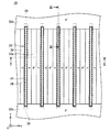
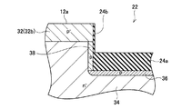
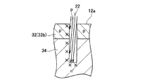
12 :半導体基板
22 :トレンチ
24 :ゲート絶縁層
24a :底部絶縁層
24b :側面絶縁膜
26 :ゲート電極
28 :層間絶縁膜
30 :ソース領域
32 :ボディ領域
34 :ドリフト領域
35 :ドレイン領域
36 :底部領域
38 :接続領域
70 :上部電極
72 :下部電極
Claims (1)
- スイッチング素子であって、
半導体基板と、
前記半導体基板の上面に設けられたトレンチと、
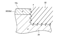
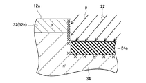
前記トレンチの底部に配置されており、前記トレンチの底面と前記底面近傍の前記トレンチの側面を覆っている底部絶縁層と、
前記底部絶縁層の上部で前記トレンチの前記側面を覆っており、前記底部絶縁層の上面と下面の間の幅よりも小さい厚みを備える側面絶縁膜と、
前記トレンチ内に配置されており、前記底部絶縁層と前記側面絶縁膜によって前記半導体基板から絶縁されているゲート電極、
を有しており、
前記半導体基板が、
前記側面絶縁膜に接している第1導電型の第1領域と、
前記第1領域の下側で前記側面絶縁膜に接している第2導電型のボディ領域と、
前記ボディ領域の下側で前記側面絶縁膜と前記底部絶縁層に接しており、前記ボディ領域によって前記第1領域から分離されている第1導電型の第2領域と、
前記トレンチの前記底面において前記底部絶縁層に接している第2導電型の底部領域と、
前記トレンチの前記側面に沿って伸びており、前記底部絶縁層と前記側面絶縁膜に接しており、前記ボディ領域と前記底部領域とを接続している第2導電型の接続領域、
を有しており、
前記接続領域が、前記トレンチの前記側面のうちの前記トレンチの短手方向の端部に位置する側面の一部において前記底部絶縁層と前記側面絶縁膜に接しており、
前記接続領域に接している範囲の前記側面絶縁膜が、前記第2領域に接している範囲の前記側面絶縁膜よりも厚く、
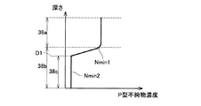
前記底部絶縁層と前記接続領域が接している深さ範囲内の前記接続領域に、前記側面絶縁膜と前記接続領域が接している深さ範囲内の前記接続領域における第2導電型不純物濃度の最低値よりも低い第2導電型不純物濃度を有する深さ範囲が存在する、
スイッチング素子。
Priority Applications (3)
| Application Number | Priority Date | Filing Date | Title |
|---|---|---|---|
| JP2016082975A JP6606007B2 (ja) | 2016-04-18 | 2016-04-18 | スイッチング素子 |
| US16/093,882 US20190109187A1 (en) | 2016-04-18 | 2017-04-18 | Semiconductor switching element |
| PCT/IB2017/000425 WO2017182864A1 (en) | 2016-04-18 | 2017-04-18 | Semiconductor switching element |
Applications Claiming Priority (1)
| Application Number | Priority Date | Filing Date | Title |
|---|---|---|---|
| JP2016082975A JP6606007B2 (ja) | 2016-04-18 | 2016-04-18 | スイッチング素子 |
Publications (2)
| Publication Number | Publication Date |
|---|---|
| JP2017195224A JP2017195224A (ja) | 2017-10-26 |
| JP6606007B2 true JP6606007B2 (ja) | 2019-11-13 |
Family
ID=58664740
Family Applications (1)
| Application Number | Title | Priority Date | Filing Date |
|---|---|---|---|
| JP2016082975A Expired - Fee Related JP6606007B2 (ja) | 2016-04-18 | 2016-04-18 | スイッチング素子 |
Country Status (3)
| Country | Link |
|---|---|
| US (1) | US20190109187A1 (ja) |
| JP (1) | JP6606007B2 (ja) |
| WO (1) | WO2017182864A1 (ja) |
Families Citing this family (10)
| Publication number | Priority date | Publication date | Assignee | Title |
|---|---|---|---|---|
| JP2019087612A (ja) * | 2017-11-06 | 2019-06-06 | トヨタ自動車株式会社 | 半導体装置の製造方法 |
| JP2019087611A (ja) * | 2017-11-06 | 2019-06-06 | トヨタ自動車株式会社 | スイッチング素子とその製造方法 |
| JP2019125625A (ja) * | 2018-01-12 | 2019-07-25 | トヨタ自動車株式会社 | 半導体装置及び半導体装置の製造方法 |
| JP2019129290A (ja) * | 2018-01-26 | 2019-08-01 | トヨタ自動車株式会社 | 半導体素子 |
| JP7107718B2 (ja) * | 2018-03-28 | 2022-07-27 | 株式会社デンソー | スイッチング素子の製造方法 |
| IT201900013416A1 (it) * | 2019-07-31 | 2021-01-31 | St Microelectronics Srl | Dispositivo di potenza a bilanciamento di carica e procedimento di fabbricazione del dispositivo di potenza a bilanciamento di carica |
| JP7207361B2 (ja) * | 2020-04-22 | 2023-01-18 | 株式会社デンソー | 半導体装置 |
| US12080790B2 (en) * | 2020-10-28 | 2024-09-03 | Wolfspeed, Inc. | Power semiconductor devices including angled gate trenches |
| JP7717010B2 (ja) * | 2022-03-08 | 2025-08-01 | 株式会社デンソー | 半導体装置 |
| JP7756607B2 (ja) | 2022-08-22 | 2025-10-20 | 株式会社東芝 | 半導体装置及びその製造方法 |
Family Cites Families (8)
| Publication number | Priority date | Publication date | Assignee | Title |
|---|---|---|---|---|
| US6342709B1 (en) * | 1997-12-10 | 2002-01-29 | The Kansai Electric Power Co., Inc. | Insulated gate semiconductor device |
| JP4453671B2 (ja) * | 2006-03-08 | 2010-04-21 | トヨタ自動車株式会社 | 絶縁ゲート型半導体装置およびその製造方法 |
| JP5206107B2 (ja) * | 2007-09-06 | 2013-06-12 | トヨタ自動車株式会社 | 半導体装置 |
| JP2011134910A (ja) * | 2009-12-24 | 2011-07-07 | Rohm Co Ltd | SiC電界効果トランジスタ |
| JP5920970B2 (ja) * | 2011-11-30 | 2016-05-24 | ローム株式会社 | 半導体装置 |
| JP5751213B2 (ja) * | 2012-06-14 | 2015-07-22 | 株式会社デンソー | 炭化珪素半導体装置およびその製造方法 |
| EP2924739B1 (en) * | 2012-11-21 | 2019-08-14 | Toyota Jidosha Kabushiki Kaisha | Semiconductor device |
| DE102014107325B4 (de) * | 2014-05-23 | 2023-08-10 | Infineon Technologies Ag | Halbleiterbauelement und verfahren zum herstellen eines halbleiterbauelements |
-
2016
- 2016-04-18 JP JP2016082975A patent/JP6606007B2/ja not_active Expired - Fee Related
-
2017
- 2017-04-18 US US16/093,882 patent/US20190109187A1/en not_active Abandoned
- 2017-04-18 WO PCT/IB2017/000425 patent/WO2017182864A1/en not_active Ceased
Also Published As
| Publication number | Publication date |
|---|---|
| JP2017195224A (ja) | 2017-10-26 |
| WO2017182864A1 (en) | 2017-10-26 |
| US20190109187A1 (en) | 2019-04-11 |
Similar Documents
| Publication | Publication Date | Title |
|---|---|---|
| JP6606007B2 (ja) | スイッチング素子 | |
| CN104054179B (zh) | 半导体装置 | |
| JP6763727B2 (ja) | スイッチング装置とその製造方法 | |
| JP5480084B2 (ja) | 半導体装置 | |
| JP2019087611A (ja) | スイッチング素子とその製造方法 | |
| JP5537359B2 (ja) | 半導体装置 | |
| CN104900690A (zh) | 半导体装置 | |
| US20120068221A1 (en) | Semiconductor device | |
| JP6720818B2 (ja) | 半導体装置 | |
| CN107210299A (zh) | 半导体装置 | |
| JP2019079833A (ja) | スイッチング素子とその製造方法 | |
| WO2016009736A1 (ja) | スイッチング素子 | |
| JP2018056304A (ja) | スイッチング装置とその製造方法 | |
| CN108292680B (zh) | 碳化硅半导体装置 | |
| JP2017191817A (ja) | スイッチング素子の製造方法 | |
| CN102468298A (zh) | 带有集成箝位电路的累积型场效应管 | |
| JP2022139077A (ja) | 電界効果トランジスタ | |
| JP6560141B2 (ja) | スイッチング素子 | |
| JP2017174961A (ja) | スイッチング素子の製造方法 | |
| JP6560142B2 (ja) | スイッチング素子 | |
| JP2020064910A (ja) | スイッチング素子 | |
| JP7147510B2 (ja) | スイッチング素子 | |
| JP2024137200A (ja) | 電界効果トランジスタ | |
| JP7326991B2 (ja) | スイッチング素子 | |
| KR20190100598A (ko) | 향상된 채널 이동도를 갖는 전력 반도체 및 그 제조 방법 |
Legal Events
| Date | Code | Title | Description |
|---|---|---|---|
| A621 | Written request for application examination |
Free format text: JAPANESE INTERMEDIATE CODE: A621 Effective date: 20180605 |
|
| A977 | Report on retrieval |
Free format text: JAPANESE INTERMEDIATE CODE: A971007 Effective date: 20190225 |
|
| A131 | Notification of reasons for refusal |
Free format text: JAPANESE INTERMEDIATE CODE: A131 Effective date: 20190305 |
|
| A521 | Request for written amendment filed |
Free format text: JAPANESE INTERMEDIATE CODE: A523 Effective date: 20190424 |
|
| TRDD | Decision of grant or rejection written | ||
| A01 | Written decision to grant a patent or to grant a registration (utility model) |
Free format text: JAPANESE INTERMEDIATE CODE: A01 Effective date: 20190924 |
|
| A61 | First payment of annual fees (during grant procedure) |
Free format text: JAPANESE INTERMEDIATE CODE: A61 Effective date: 20191017 |
|
| R151 | Written notification of patent or utility model registration |
Ref document number: 6606007 Country of ref document: JP Free format text: JAPANESE INTERMEDIATE CODE: R151 |
|
| S111 | Request for change of ownership or part of ownership |
Free format text: JAPANESE INTERMEDIATE CODE: R313117 |
|
| R350 | Written notification of registration of transfer |
Free format text: JAPANESE INTERMEDIATE CODE: R350 |
|
| R250 | Receipt of annual fees |
Free format text: JAPANESE INTERMEDIATE CODE: R250 |
|
| R250 | Receipt of annual fees |
Free format text: JAPANESE INTERMEDIATE CODE: R250 |
|
| LAPS | Cancellation because of no payment of annual fees |