JP6604911B2 - エッチング処理方法 - Google Patents
エッチング処理方法 Download PDFInfo
- Publication number
- JP6604911B2 JP6604911B2 JP2016124600A JP2016124600A JP6604911B2 JP 6604911 B2 JP6604911 B2 JP 6604911B2 JP 2016124600 A JP2016124600 A JP 2016124600A JP 2016124600 A JP2016124600 A JP 2016124600A JP 6604911 B2 JP6604911 B2 JP 6604911B2
- Authority
- JP
- Japan
- Prior art keywords
- etching
- gas
- frequency power
- containing gas
- plasma
- Prior art date
- Legal status (The legal status is an assumption and is not a legal conclusion. Google has not performed a legal analysis and makes no representation as to the accuracy of the status listed.)
- Active
Links
Images


Classifications
-
- H—ELECTRICITY
- H01—ELECTRIC ELEMENTS
- H01L—SEMICONDUCTOR DEVICES NOT COVERED BY CLASS H10
- H01L21/00—Processes or apparatus adapted for the manufacture or treatment of semiconductor or solid state devices or of parts thereof
- H01L21/02—Manufacture or treatment of semiconductor devices or of parts thereof
- H01L21/04—Manufacture or treatment of semiconductor devices or of parts thereof the devices having at least one potential-jump barrier or surface barrier, e.g. PN junction, depletion layer or carrier concentration layer
- H01L21/18—Manufacture or treatment of semiconductor devices or of parts thereof the devices having at least one potential-jump barrier or surface barrier, e.g. PN junction, depletion layer or carrier concentration layer the devices having semiconductor bodies comprising elements of Group IV of the Periodic System or AIIIBV compounds with or without impurities, e.g. doping materials
- H01L21/30—Treatment of semiconductor bodies using processes or apparatus not provided for in groups H01L21/20 - H01L21/26
- H01L21/31—Treatment of semiconductor bodies using processes or apparatus not provided for in groups H01L21/20 - H01L21/26 to form insulating layers thereon, e.g. for masking or by using photolithographic techniques; After treatment of these layers; Selection of materials for these layers
- H01L21/3105—After-treatment
- H01L21/311—Etching the insulating layers by chemical or physical means
- H01L21/31105—Etching inorganic layers
- H01L21/31111—Etching inorganic layers by chemical means
- H01L21/31116—Etching inorganic layers by chemical means by dry-etching
-
- H—ELECTRICITY
- H01—ELECTRIC ELEMENTS
- H01J—ELECTRIC DISCHARGE TUBES OR DISCHARGE LAMPS
- H01J37/00—Discharge tubes with provision for introducing objects or material to be exposed to the discharge, e.g. for the purpose of examination or processing thereof
- H01J37/32—Gas-filled discharge tubes
- H01J37/32009—Arrangements for generation of plasma specially adapted for examination or treatment of objects, e.g. plasma sources
- H01J37/32082—Radio frequency generated discharge
- H01J37/32091—Radio frequency generated discharge the radio frequency energy being capacitively coupled to the plasma
-
- H—ELECTRICITY
- H01—ELECTRIC ELEMENTS
- H01J—ELECTRIC DISCHARGE TUBES OR DISCHARGE LAMPS
- H01J37/00—Discharge tubes with provision for introducing objects or material to be exposed to the discharge, e.g. for the purpose of examination or processing thereof
- H01J37/32—Gas-filled discharge tubes
- H01J37/32009—Arrangements for generation of plasma specially adapted for examination or treatment of objects, e.g. plasma sources
- H01J37/32082—Radio frequency generated discharge
- H01J37/32137—Radio frequency generated discharge controlling of the discharge by modulation of energy
- H01J37/32155—Frequency modulation
- H01J37/32165—Plural frequencies
-
- H—ELECTRICITY
- H01—ELECTRIC ELEMENTS
- H01J—ELECTRIC DISCHARGE TUBES OR DISCHARGE LAMPS
- H01J37/00—Discharge tubes with provision for introducing objects or material to be exposed to the discharge, e.g. for the purpose of examination or processing thereof
- H01J37/32—Gas-filled discharge tubes
- H01J37/32431—Constructional details of the reactor
- H01J37/3244—Gas supply means
-
- H—ELECTRICITY
- H01—ELECTRIC ELEMENTS
- H01J—ELECTRIC DISCHARGE TUBES OR DISCHARGE LAMPS
- H01J37/00—Discharge tubes with provision for introducing objects or material to be exposed to the discharge, e.g. for the purpose of examination or processing thereof
- H01J37/32—Gas-filled discharge tubes
- H01J37/32431—Constructional details of the reactor
- H01J37/32715—Workpiece holder
- H01J37/32724—Temperature
-
- H—ELECTRICITY
- H01—ELECTRIC ELEMENTS
- H01J—ELECTRIC DISCHARGE TUBES OR DISCHARGE LAMPS
- H01J37/00—Discharge tubes with provision for introducing objects or material to be exposed to the discharge, e.g. for the purpose of examination or processing thereof
- H01J37/32—Gas-filled discharge tubes
- H01J37/32431—Constructional details of the reactor
- H01J37/32798—Further details of plasma apparatus not provided for in groups H01J37/3244 - H01J37/32788; special provisions for cleaning or maintenance of the apparatus
- H01J37/32816—Pressure
-
- H—ELECTRICITY
- H01—ELECTRIC ELEMENTS
- H01L—SEMICONDUCTOR DEVICES NOT COVERED BY CLASS H10
- H01L21/00—Processes or apparatus adapted for the manufacture or treatment of semiconductor or solid state devices or of parts thereof
- H01L21/02—Manufacture or treatment of semiconductor devices or of parts thereof
- H01L21/02104—Forming layers
- H01L21/02107—Forming insulating materials on a substrate
- H01L21/02109—Forming insulating materials on a substrate characterised by the type of layer, e.g. type of material, porous/non-porous, pre-cursors, mixtures or laminates
- H01L21/022—Forming insulating materials on a substrate characterised by the type of layer, e.g. type of material, porous/non-porous, pre-cursors, mixtures or laminates the layer being a laminate, i.e. composed of sublayers, e.g. stacks of alternating high-k metal oxides
-
- H—ELECTRICITY
- H01—ELECTRIC ELEMENTS
- H01L—SEMICONDUCTOR DEVICES NOT COVERED BY CLASS H10
- H01L21/00—Processes or apparatus adapted for the manufacture or treatment of semiconductor or solid state devices or of parts thereof
- H01L21/02—Manufacture or treatment of semiconductor devices or of parts thereof
- H01L21/04—Manufacture or treatment of semiconductor devices or of parts thereof the devices having at least one potential-jump barrier or surface barrier, e.g. PN junction, depletion layer or carrier concentration layer
- H01L21/18—Manufacture or treatment of semiconductor devices or of parts thereof the devices having at least one potential-jump barrier or surface barrier, e.g. PN junction, depletion layer or carrier concentration layer the devices having semiconductor bodies comprising elements of Group IV of the Periodic System or AIIIBV compounds with or without impurities, e.g. doping materials
- H01L21/30—Treatment of semiconductor bodies using processes or apparatus not provided for in groups H01L21/20 - H01L21/26
- H01L21/302—Treatment of semiconductor bodies using processes or apparatus not provided for in groups H01L21/20 - H01L21/26 to change their surface-physical characteristics or shape, e.g. etching, polishing, cutting
- H01L21/306—Chemical or electrical treatment, e.g. electrolytic etching
- H01L21/3065—Plasma etching; Reactive-ion etching
-
- H—ELECTRICITY
- H01—ELECTRIC ELEMENTS
- H01L—SEMICONDUCTOR DEVICES NOT COVERED BY CLASS H10
- H01L21/00—Processes or apparatus adapted for the manufacture or treatment of semiconductor or solid state devices or of parts thereof
- H01L21/02—Manufacture or treatment of semiconductor devices or of parts thereof
- H01L21/04—Manufacture or treatment of semiconductor devices or of parts thereof the devices having at least one potential-jump barrier or surface barrier, e.g. PN junction, depletion layer or carrier concentration layer
- H01L21/18—Manufacture or treatment of semiconductor devices or of parts thereof the devices having at least one potential-jump barrier or surface barrier, e.g. PN junction, depletion layer or carrier concentration layer the devices having semiconductor bodies comprising elements of Group IV of the Periodic System or AIIIBV compounds with or without impurities, e.g. doping materials
- H01L21/30—Treatment of semiconductor bodies using processes or apparatus not provided for in groups H01L21/20 - H01L21/26
- H01L21/31—Treatment of semiconductor bodies using processes or apparatus not provided for in groups H01L21/20 - H01L21/26 to form insulating layers thereon, e.g. for masking or by using photolithographic techniques; After treatment of these layers; Selection of materials for these layers
- H01L21/3205—Deposition of non-insulating-, e.g. conductive- or resistive-, layers on insulating layers; After-treatment of these layers
- H01L21/321—After treatment
- H01L21/3213—Physical or chemical etching of the layers, e.g. to produce a patterned layer from a pre-deposited extensive layer
- H01L21/32133—Physical or chemical etching of the layers, e.g. to produce a patterned layer from a pre-deposited extensive layer by chemical means only
- H01L21/32135—Physical or chemical etching of the layers, e.g. to produce a patterned layer from a pre-deposited extensive layer by chemical means only by vapour etching only
- H01L21/32136—Physical or chemical etching of the layers, e.g. to produce a patterned layer from a pre-deposited extensive layer by chemical means only by vapour etching only using plasmas
-
- H—ELECTRICITY
- H01—ELECTRIC ELEMENTS
- H01L—SEMICONDUCTOR DEVICES NOT COVERED BY CLASS H10
- H01L21/00—Processes or apparatus adapted for the manufacture or treatment of semiconductor or solid state devices or of parts thereof
- H01L21/02—Manufacture or treatment of semiconductor devices or of parts thereof
- H01L21/04—Manufacture or treatment of semiconductor devices or of parts thereof the devices having at least one potential-jump barrier or surface barrier, e.g. PN junction, depletion layer or carrier concentration layer
- H01L21/18—Manufacture or treatment of semiconductor devices or of parts thereof the devices having at least one potential-jump barrier or surface barrier, e.g. PN junction, depletion layer or carrier concentration layer the devices having semiconductor bodies comprising elements of Group IV of the Periodic System or AIIIBV compounds with or without impurities, e.g. doping materials
- H01L21/30—Treatment of semiconductor bodies using processes or apparatus not provided for in groups H01L21/20 - H01L21/26
- H01L21/324—Thermal treatment for modifying the properties of semiconductor bodies, e.g. annealing, sintering
-
- H—ELECTRICITY
- H01—ELECTRIC ELEMENTS
- H01L—SEMICONDUCTOR DEVICES NOT COVERED BY CLASS H10
- H01L21/00—Processes or apparatus adapted for the manufacture or treatment of semiconductor or solid state devices or of parts thereof
- H01L21/67—Apparatus specially adapted for handling semiconductor or electric solid state devices during manufacture or treatment thereof; Apparatus specially adapted for handling wafers during manufacture or treatment of semiconductor or electric solid state devices or components ; Apparatus not specifically provided for elsewhere
- H01L21/67005—Apparatus not specifically provided for elsewhere
- H01L21/67011—Apparatus for manufacture or treatment
- H01L21/67017—Apparatus for fluid treatment
- H01L21/67063—Apparatus for fluid treatment for etching
- H01L21/67069—Apparatus for fluid treatment for etching for drying etching
-
- H—ELECTRICITY
- H01—ELECTRIC ELEMENTS
- H01L—SEMICONDUCTOR DEVICES NOT COVERED BY CLASS H10
- H01L21/00—Processes or apparatus adapted for the manufacture or treatment of semiconductor or solid state devices or of parts thereof
- H01L21/67—Apparatus specially adapted for handling semiconductor or electric solid state devices during manufacture or treatment thereof; Apparatus specially adapted for handling wafers during manufacture or treatment of semiconductor or electric solid state devices or components ; Apparatus not specifically provided for elsewhere
- H01L21/67005—Apparatus not specifically provided for elsewhere
- H01L21/67242—Apparatus for monitoring, sorting or marking
- H01L21/67248—Temperature monitoring
-
- H—ELECTRICITY
- H01—ELECTRIC ELEMENTS
- H01J—ELECTRIC DISCHARGE TUBES OR DISCHARGE LAMPS
- H01J2237/00—Discharge tubes exposing object to beam, e.g. for analysis treatment, etching, imaging
- H01J2237/20—Positioning, supporting, modifying or maintaining the physical state of objects being observed or treated
- H01J2237/2001—Maintaining constant desired temperature
-
- H—ELECTRICITY
- H01—ELECTRIC ELEMENTS
- H01J—ELECTRIC DISCHARGE TUBES OR DISCHARGE LAMPS
- H01J2237/00—Discharge tubes exposing object to beam, e.g. for analysis treatment, etching, imaging
- H01J2237/32—Processing objects by plasma generation
- H01J2237/33—Processing objects by plasma generation characterised by the type of processing
- H01J2237/334—Etching
-
- H—ELECTRICITY
- H01—ELECTRIC ELEMENTS
- H01J—ELECTRIC DISCHARGE TUBES OR DISCHARGE LAMPS
- H01J37/00—Discharge tubes with provision for introducing objects or material to be exposed to the discharge, e.g. for the purpose of examination or processing thereof
- H01J37/32—Gas-filled discharge tubes
- H01J37/32431—Constructional details of the reactor
- H01J37/32623—Mechanical discharge control means
- H01J37/32642—Focus rings
-
- H—ELECTRICITY
- H01—ELECTRIC ELEMENTS
- H01J—ELECTRIC DISCHARGE TUBES OR DISCHARGE LAMPS
- H01J37/00—Discharge tubes with provision for introducing objects or material to be exposed to the discharge, e.g. for the purpose of examination or processing thereof
- H01J37/32—Gas-filled discharge tubes
- H01J37/32431—Constructional details of the reactor
- H01J37/32798—Further details of plasma apparatus not provided for in groups H01J37/3244 - H01J37/32788; special provisions for cleaning or maintenance of the apparatus
- H01J37/32816—Pressure
- H01J37/32834—Exhausting
Description
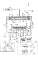
まず、プラズマ処理装置1の一例について、図1を参照しながら説明する。本実施形態にかかるプラズマ処理装置1は、平行平板型のプラズマ処理装置であり、略円筒形の処理容器10を有している。処理容器10の内面には、アルマイト処理(陽極酸化処理)が施されている。処理容器10の内部は、プラズマによりエッチング処理や成膜処理等のプラズマ処理が行われる処理室となっている。
<第1実施形態>
[極低温におけるエッチング]
以下では、第1実施形態に係る極低温におけるエッチング処理について説明し、そのエッチング処理の結果の一例を、比較例1,2に係るエッチング処理の結果の一例と比較する。
比較例1では、以下のプロセス条件にてシリコン酸化膜(SiO2)とシリコン窒化膜(SiN)とを積層させた積層膜12がエッチングされる。積層膜12は、組成の異なるシリコン含有膜を積層した積層膜の一例である。積層膜12の上部にはアモルファスカーボン膜11が形成され、マスクとして機能する。ただし、マスクは、アモルファスカーボン膜に限らず、有機膜であってもよい。
・プロセス条件(比較例1)
ウェハ温度 −40℃以下(チラー温度 −60℃)
ガス CF4(四フッ化炭素)/CH4(メタン)/O2(酸素)
第1高周波電力HF 2500W、連続波
第2高周波電力LF 4000W、連続波
(比較例2)
比較例2では、以下のプロセス条件にて積層膜12がエッチングされる。
・プロセス条件(比較例2)
ウェハ温度 −40℃以下(チラー温度 −60℃)
ガス H2(水素)/CF4(四フッ化炭素)/CHF3(三フッ化メタン)
第1高周波電力HF 2500W、連続波
第2高周波電力LF 4000W、連続波
図2(a)は、比較例1のエッチング結果の一例を示す。図2(b)は、比較例2のエッチング結果の一例を示す。図2(a)及び図2(b)のそれぞれの結果は、アモルファスカーボン膜11をマスクとして積層膜12をエッチングしたときのホールの縦断面のエッチング形状と、アモルファスカーボン膜11を上方から見たときのアモルファスカーボン膜11の間口の形状を示す。また、各形状の下の数値は、エッチングの深さ(Depth)、マスク選択比、エッチングレート(ER)、ボーイング(Bowing)を示す。ボーイングは、ホールの横方向の幅が最も広い部分の数値である。
第1実施形態では、以下のプロセス条件にて積層膜12のエッチングが行われる。
・プロセス条件(第1実施形態)
ウェハ温度 −40℃以下(チラー温度 −60℃)
ガス SF6(六フッ化硫黄)/H2(水素)
第1高周波電力HF 2500W、連続波
第2高周波電力LF 4000W、連続波
処理容器内の圧力 15〜25mTorr(2.0〜3.3Pa)
なお、第1実施形態及び後述する実施形態のプロセス条件では、第1高周波電力HF及び第2高周波電力LFが印加されているが、これに限らず、第1高周波電力HFのみを印加するようにしてもよい。
第2実施形態では、以下のプロセス条件にて積層膜12がエッチングされる。
・プロセス条件(第2実施形態)
ウェハ温度 −40℃以下(チラー温度 −60℃)
ガス SF6(六フッ化硫黄)/CH4(メタン)
第1高周波電力HF 2500W、連続波
第2高周波電力LF 4000W、連続波
処理容器内の圧力 15〜25mTorr(2.0〜3.3Pa)
図3(c)は、第2実施形態のエッチング結果の一例を示す。図3(a)及び図3(b)は、図2(a)及び図2(b)の比較例1,2と同じエッチング結果を図示している。図3(c)に示す第2実施形態のエッチング結果では、図3(a)及び図3(b)の比較例1,2と比べて、エッチングの深さ(Depth)とエッチングレート(ER)とを維持しつつ、サイドエッチングが抑制され、エッチング形状が改善されている。
次に、変形例に係るエッチング処理の一例について、図4を参照して説明する。図4は、変形例に係るエッチング処理の一例を示すフローチャートである。本処理が開始されると、制御部100は、ウェハ表面の温度を−35℃以下の極低温に制御する(ステップS10)。次に、制御部100は、フッ化硫黄含有ガス及び水素含有ガスを処理容器10の内部に供給する(ステップS12)。ここで供給するガスは、例えば、第1実施形態において供給した六フッ化硫黄(SF6)ガス及び水素(H2)ガスであってもよいし、第2実施形態において供給した六フッ化硫黄(SF6)ガス及びCH4(メタン)ガスであってもよい。
図5は、図4の第1高周波電力HFのオン・オフを繰り返して行われる間欠エッチングにおけるウェハW表面の温度の遷移の一例を示す。ウェハWが静電チャック106に保持された状態で第1高周波電力HFを印加すると、プラズマが生成され、エッチング処理が開始される。このようにして第1高周波電力HFを印加し、プラズマが生成されると、そのプラズマからの入熱(プラズマオン)によりウェハWの温度は緩やかに上昇する。しかしながら、チラー107の温度を−60℃以下に制御することでウェハWの温度を−35℃以下に維持できることがわかる。
図6(c)は、チラー107の温度を−70℃に制御することで、ウェハWの温度を−40℃以下に制御したときの一実施形態に係る極低温プロセスにおけるエッチング結果の一例を示す。本実施形態では、以下のプロセス条件にて、アモルファスカーボン膜11をマスクとして、シリコン酸化膜とシリコン窒化膜とを積層した積層膜12のエッチングが行われる。
・プロセス条件(第1実施形態)
ウェハ温度 −40℃以下(チラー温度 −70℃)
ガス SF6(六フッ化硫黄)/H2(水素)/CH4(メタン)
第1高周波電力HF 2500W、連続波
第2高周波電力LF 4000W、連続波
処理容器内の圧力 15〜25mTorr(2.0〜3.3Pa)
上記各実施形態及び変形例に係るエッチング処理では、水素含有ガスの一例としてH2ガス及びCH4ガスの少なくともいずれかが供給され、フッ化硫黄含有ガスの一例としてSF6ガスが供給された。その結果、H2ガス及びCH4ガスに含まれるH(水素)と、積層膜12中のシリコン酸化膜に含まれるO(酸素)により、H2Oが反応生成物として発生される。
10 処理容器
11 アモルファスカーボン膜
12 積層膜
15 ガス供給源
20 載置台
25 ガスシャワーヘッド
32 第1高周波電源
34 第2高周波電源
65 排気装置
70 可変直流電源
100 制御部
104 支持体
104a 冷媒流路
106 静電チャック
106a チャック電極
107 チラー
108 フォーカスリング
Claims (10)
- エッチング処理方法であって、
シリコン酸化膜及びシリコン窒化膜が交互に積層する積層膜を有する基板を提供する工程と、
前記基板の温度を−35℃以下に設定する工程と、
第1高周波の電力を出力し、フッ化硫黄含有ガス及び水素含有ガスを含み、フルオロカーボンガスを含まないガスからプラズマを生成し、前記積層膜をエッチングする工程と、を備える、エッチング処理方法。 - 水素含有ガスは、ハイドロカーボン含有ガスである、
請求項1に記載のエッチング処理方法。 - 前記ハイドロカーボン含有ガスは、CH4(メタン)、C2H8、C2H2(アセチレン)、C2H4(エチレン)、C2H6(エタン)、C3H6(プロピレン)、C3H8(プロパン)、C3H4(プロピン)の少なくともいずれかである、
請求項2に記載のエッチング処理方法。 - 水素含有ガスは、ハイドロフルオロカーボン含有ガスである、
請求項1に記載のエッチング処理方法。 - 前記ハイドロフルオロカーボン含有ガスは、CH2F2(二フッ化メタン)、CH3F(フルオロメタン)、CHF3(三フッ化メタン)の少なくともいずれかである、
請求項4に記載のエッチング処理方法。 - 前記プラズマは、容量結合型プラズマ(CCP)である、
請求項1〜5のいずれか一項に記載のエッチング処理方法。 - 前記フッ化硫黄含有ガスは、SF6(六フッ化硫黄)である、
請求項1〜6のいずれか一項に記載のエッチング処理方法。 - 前記基板のエッチングが行われる処理容器の内部を、15〜25mTorr(2.0〜3.3Pa)に制御する、
請求項1〜7のいずれか一項に記載のエッチング処理方法。 - エッチング処理方法であって、
組成の異なるシリコン含有膜を積層した積層膜を有する基板を提供する工程と、
前記基板の温度を−35℃以下に設定する工程と、
第1高周波の電力を出力し、フッ化硫黄含有ガス及びハイドロカーボンガスを含み、フルオロカーボンガスを含まないガスからプラズマを生成し、前記積層膜をエッチングする工程と、を含む、エッチング処理方法。 - 前記プラズマは、容量結合型プラズマ(CCP)である、
請求項9に記載のエッチング処理方法。
Priority Applications (4)
| Application Number | Priority Date | Filing Date | Title |
|---|---|---|---|
| JP2016124600A JP6604911B2 (ja) | 2016-06-23 | 2016-06-23 | エッチング処理方法 |
| TW106119401A TWI731101B (zh) | 2016-06-23 | 2017-06-12 | 蝕刻處理方法 |
| US15/625,165 US10692729B2 (en) | 2016-06-23 | 2017-06-16 | Etching process method |
| KR1020170079056A KR102584336B1 (ko) | 2016-06-23 | 2017-06-22 | 에칭 처리 방법 |
Applications Claiming Priority (1)
| Application Number | Priority Date | Filing Date | Title |
|---|---|---|---|
| JP2016124600A JP6604911B2 (ja) | 2016-06-23 | 2016-06-23 | エッチング処理方法 |
Publications (3)
| Publication Number | Publication Date |
|---|---|
| JP2017228690A JP2017228690A (ja) | 2017-12-28 |
| JP2017228690A5 JP2017228690A5 (ja) | 2019-02-21 |
| JP6604911B2 true JP6604911B2 (ja) | 2019-11-13 |
Family
ID=60677880
Family Applications (1)
| Application Number | Title | Priority Date | Filing Date |
|---|---|---|---|
| JP2016124600A Active JP6604911B2 (ja) | 2016-06-23 | 2016-06-23 | エッチング処理方法 |
Country Status (4)
| Country | Link |
|---|---|
| US (1) | US10692729B2 (ja) |
| JP (1) | JP6604911B2 (ja) |
| KR (1) | KR102584336B1 (ja) |
| TW (1) | TWI731101B (ja) |
Families Citing this family (16)
| Publication number | Priority date | Publication date | Assignee | Title |
|---|---|---|---|---|
| KR20190098922A (ko) * | 2018-02-15 | 2019-08-23 | 도쿄엘렉트론가부시키가이샤 | 플라즈마 에칭 방법 및 플라즈마 에칭 장치 |
| JP7158252B2 (ja) * | 2018-02-15 | 2022-10-21 | 東京エレクトロン株式会社 | プラズマエッチング方法及びプラズマエッチング装置 |
| JP2019179889A (ja) | 2018-03-30 | 2019-10-17 | 東京エレクトロン株式会社 | エッチング方法及びプラズマ処理装置 |
| TWI804638B (zh) * | 2018-06-22 | 2023-06-11 | 日商關東電化工業股份有限公司 | 使用含硫原子之氣體分子之電漿蝕刻方法 |
| KR102608957B1 (ko) | 2018-08-27 | 2023-12-01 | 삼성전자주식회사 | 플라즈마 처리 장치 |
| JP7229033B2 (ja) * | 2019-02-01 | 2023-02-27 | 東京エレクトロン株式会社 | 基板処理方法及び基板処理装置 |
| JP7222940B2 (ja) * | 2019-02-18 | 2023-02-15 | 東京エレクトロン株式会社 | エッチング方法及びプラズマ処理装置 |
| JP2020177958A (ja) * | 2019-04-15 | 2020-10-29 | 東京エレクトロン株式会社 | 基板処理方法及び基板処理装置 |
| TW202105514A (zh) * | 2019-06-13 | 2021-02-01 | 日商東京威力科創股份有限公司 | 蝕刻方法以及蝕刻裝置 |
| JP7413093B2 (ja) * | 2019-07-18 | 2024-01-15 | キオクシア株式会社 | エッチング方法、半導体製造装置、および半導体装置の製造方法 |
| US11651969B2 (en) | 2019-07-18 | 2023-05-16 | Kioxia Corporation | Etching method, semiconductor manufacturing apparatus, and method of manufacturing semiconductor device |
| CN113785382B (zh) * | 2020-04-10 | 2023-10-27 | 株式会社日立高新技术 | 蚀刻方法 |
| US11171012B1 (en) | 2020-05-27 | 2021-11-09 | Tokyo Electron Limited | Method and apparatus for formation of protective sidewall layer for bow reduction |
| US11087989B1 (en) | 2020-06-18 | 2021-08-10 | Applied Materials, Inc. | Cryogenic atomic layer etch with noble gases |
| WO2022041198A1 (zh) * | 2020-08-31 | 2022-03-03 | 深圳大学 | 一种三维堆叠存储芯片的温度变化计算方法 |
| US20220404247A1 (en) * | 2021-06-21 | 2022-12-22 | Fei Company | Vibration-free cryogenic cooling |
Family Cites Families (16)
| Publication number | Priority date | Publication date | Assignee | Title |
|---|---|---|---|---|
| JPS512096A (ja) * | 1974-06-03 | 1976-01-09 | Tipton Mfg Co | Zenjidoreshipurokenmaki |
| JPH0316210A (ja) | 1989-06-14 | 1991-01-24 | Hitachi Ltd | 低温ドライエッチング方法 |
| KR910010516A (ko) * | 1989-11-15 | 1991-06-29 | 아오이 죠이치 | 반도체 메모리장치 |
| JP3006048B2 (ja) | 1990-07-27 | 2000-02-07 | ソニー株式会社 | ドライエッチング方法 |
| JPH04354331A (ja) * | 1991-05-31 | 1992-12-08 | Sony Corp | ドライエッチング方法 |
| JPH07147273A (ja) * | 1993-11-24 | 1995-06-06 | Tokyo Electron Ltd | エッチング処理方法 |
| JPH07263415A (ja) * | 1994-03-18 | 1995-10-13 | Fujitsu Ltd | 半導体装置の製造方法 |
| US6211092B1 (en) * | 1998-07-09 | 2001-04-03 | Applied Materials, Inc. | Counterbore dielectric plasma etch process particularly useful for dual damascene |
| JP4538209B2 (ja) | 2003-08-28 | 2010-09-08 | 株式会社日立ハイテクノロジーズ | 半導体装置の製造方法 |
| JP4653603B2 (ja) * | 2005-09-13 | 2011-03-16 | 株式会社日立ハイテクノロジーズ | プラズマエッチング方法 |
| US8771539B2 (en) * | 2011-02-22 | 2014-07-08 | Applied Materials, Inc. | Remotely-excited fluorine and water vapor etch |
| JP2013030531A (ja) * | 2011-07-27 | 2013-02-07 | Central Glass Co Ltd | ドライエッチング剤 |
| US8598040B2 (en) * | 2011-09-06 | 2013-12-03 | Lam Research Corporation | ETCH process for 3D flash structures |
| JP6211947B2 (ja) * | 2013-07-31 | 2017-10-11 | 東京エレクトロン株式会社 | 半導体装置の製造方法 |
| JP6454492B2 (ja) * | 2014-08-08 | 2019-01-16 | 東京エレクトロン株式会社 | 多層膜をエッチングする方法 |
| JP6423643B2 (ja) * | 2014-08-08 | 2018-11-14 | 東京エレクトロン株式会社 | 多層膜をエッチングする方法 |
-
2016
- 2016-06-23 JP JP2016124600A patent/JP6604911B2/ja active Active
-
2017
- 2017-06-12 TW TW106119401A patent/TWI731101B/zh active
- 2017-06-16 US US15/625,165 patent/US10692729B2/en active Active
- 2017-06-22 KR KR1020170079056A patent/KR102584336B1/ko active IP Right Grant
Also Published As
| Publication number | Publication date |
|---|---|
| US20170372916A1 (en) | 2017-12-28 |
| KR102584336B1 (ko) | 2023-10-04 |
| KR20180000692A (ko) | 2018-01-03 |
| US10692729B2 (en) | 2020-06-23 |
| JP2017228690A (ja) | 2017-12-28 |
| TWI731101B (zh) | 2021-06-21 |
| TW201810429A (zh) | 2018-03-16 |
Similar Documents
| Publication | Publication Date | Title |
|---|---|---|
| JP6604911B2 (ja) | エッチング処理方法 | |
| TWI743072B (zh) | 蝕刻方法及蝕刻裝置 | |
| EP3086359B1 (en) | Etching method | |
| US9966273B2 (en) | Plasma etching method | |
| JP6587580B2 (ja) | エッチング処理方法 | |
| JP2016122774A (ja) | エッチング処理方法及びエッチング処理装置 | |
| US20210050222A1 (en) | Plasma etching method | |
| JP6180824B2 (ja) | プラズマエッチング方法及びプラズマエッチング装置 | |
| TWI703414B (zh) | 蝕刻方法 | |
| US10128085B2 (en) | Method of plasma etching | |
| JP2016213427A (ja) | エッチング方法及びエッチング装置 | |
| JP5264383B2 (ja) | ドライエッチング方法 | |
| JP2015106587A (ja) | 静電チャックのコーティング方法及びプラズマ処理装置 |
Legal Events
| Date | Code | Title | Description |
|---|---|---|---|
| A621 | Written request for application examination |
Free format text: JAPANESE INTERMEDIATE CODE: A621 Effective date: 20180905 |
|
| A521 | Request for written amendment filed |
Free format text: JAPANESE INTERMEDIATE CODE: A523 Effective date: 20190108 |
|
| A871 | Explanation of circumstances concerning accelerated examination |
Free format text: JAPANESE INTERMEDIATE CODE: A871 Effective date: 20190108 |
|
| A975 | Report on accelerated examination |
Free format text: JAPANESE INTERMEDIATE CODE: A971005 Effective date: 20190226 |
|
| A131 | Notification of reasons for refusal |
Free format text: JAPANESE INTERMEDIATE CODE: A131 Effective date: 20190416 |
|
| A521 | Request for written amendment filed |
Free format text: JAPANESE INTERMEDIATE CODE: A523 Effective date: 20190613 |
|
| TRDD | Decision of grant or rejection written | ||
| A01 | Written decision to grant a patent or to grant a registration (utility model) |
Free format text: JAPANESE INTERMEDIATE CODE: A01 Effective date: 20190917 |
|
| A61 | First payment of annual fees (during grant procedure) |
Free format text: JAPANESE INTERMEDIATE CODE: A61 Effective date: 20191015 |
|
| R150 | Certificate of patent or registration of utility model |
Ref document number: 6604911 Country of ref document: JP Free format text: JAPANESE INTERMEDIATE CODE: R150 |
|
| R250 | Receipt of annual fees |
Free format text: JAPANESE INTERMEDIATE CODE: R250 |
|
| R250 | Receipt of annual fees |
Free format text: JAPANESE INTERMEDIATE CODE: R250 |