JP6370279B2 - ブートストラップ補償回路およびパワーモジュール - Google Patents
ブートストラップ補償回路およびパワーモジュール Download PDFInfo
- Publication number
- JP6370279B2 JP6370279B2 JP2015177234A JP2015177234A JP6370279B2 JP 6370279 B2 JP6370279 B2 JP 6370279B2 JP 2015177234 A JP2015177234 A JP 2015177234A JP 2015177234 A JP2015177234 A JP 2015177234A JP 6370279 B2 JP6370279 B2 JP 6370279B2
- Authority
- JP
- Japan
- Prior art keywords
- circuit
- potential
- mosfet
- bootstrap
- control circuit
- Prior art date
- Legal status (The legal status is an assumption and is not a legal conclusion. Google has not performed a legal analysis and makes no representation as to the accuracy of the status listed.)
- Active
Links
Images


Classifications
-
- H—ELECTRICITY
- H02—GENERATION; CONVERSION OR DISTRIBUTION OF ELECTRIC POWER
- H02M—APPARATUS FOR CONVERSION BETWEEN AC AND AC, BETWEEN AC AND DC, OR BETWEEN DC AND DC, AND FOR USE WITH MAINS OR SIMILAR POWER SUPPLY SYSTEMS; CONVERSION OF DC OR AC INPUT POWER INTO SURGE OUTPUT POWER; CONTROL OR REGULATION THEREOF
- H02M1/00—Details of apparatus for conversion
-
- H—ELECTRICITY
- H02—GENERATION; CONVERSION OR DISTRIBUTION OF ELECTRIC POWER
- H02M—APPARATUS FOR CONVERSION BETWEEN AC AND AC, BETWEEN AC AND DC, OR BETWEEN DC AND DC, AND FOR USE WITH MAINS OR SIMILAR POWER SUPPLY SYSTEMS; CONVERSION OF DC OR AC INPUT POWER INTO SURGE OUTPUT POWER; CONTROL OR REGULATION THEREOF
- H02M7/00—Conversion of ac power input into dc power output; Conversion of dc power input into ac power output
- H02M7/42—Conversion of dc power input into ac power output without possibility of reversal
- H02M7/44—Conversion of dc power input into ac power output without possibility of reversal by static converters
- H02M7/48—Conversion of dc power input into ac power output without possibility of reversal by static converters using discharge tubes with control electrode or semiconductor devices with control electrode
- H02M7/53—Conversion of dc power input into ac power output without possibility of reversal by static converters using discharge tubes with control electrode or semiconductor devices with control electrode using devices of a triode or transistor type requiring continuous application of a control signal
- H02M7/537—Conversion of dc power input into ac power output without possibility of reversal by static converters using discharge tubes with control electrode or semiconductor devices with control electrode using devices of a triode or transistor type requiring continuous application of a control signal using semiconductor devices only, e.g. single switched pulse inverters
- H02M7/5387—Conversion of dc power input into ac power output without possibility of reversal by static converters using discharge tubes with control electrode or semiconductor devices with control electrode using devices of a triode or transistor type requiring continuous application of a control signal using semiconductor devices only, e.g. single switched pulse inverters in a bridge configuration
-
- H—ELECTRICITY
- H03—ELECTRONIC CIRCUITRY
- H03K—PULSE TECHNIQUE
- H03K17/00—Electronic switching or gating, i.e. not by contact-making and –breaking
- H03K17/06—Modifications for ensuring a fully conducting state
- H03K17/063—Modifications for ensuring a fully conducting state in field-effect transistor switches
-
- H—ELECTRICITY
- H03—ELECTRONIC CIRCUITRY
- H03K—PULSE TECHNIQUE
- H03K17/00—Electronic switching or gating, i.e. not by contact-making and –breaking
- H03K17/51—Electronic switching or gating, i.e. not by contact-making and –breaking characterised by the components used
- H03K17/56—Electronic switching or gating, i.e. not by contact-making and –breaking characterised by the components used by the use, as active elements, of semiconductor devices
- H03K17/687—Electronic switching or gating, i.e. not by contact-making and –breaking characterised by the components used by the use, as active elements, of semiconductor devices the devices being field-effect transistors
- H03K17/689—Electronic switching or gating, i.e. not by contact-making and –breaking characterised by the components used by the use, as active elements, of semiconductor devices the devices being field-effect transistors with galvanic isolation between the control circuit and the output circuit
- H03K17/691—Electronic switching or gating, i.e. not by contact-making and –breaking characterised by the components used by the use, as active elements, of semiconductor devices the devices being field-effect transistors with galvanic isolation between the control circuit and the output circuit using transformer coupling
-
- H—ELECTRICITY
- H02—GENERATION; CONVERSION OR DISTRIBUTION OF ELECTRIC POWER
- H02M—APPARATUS FOR CONVERSION BETWEEN AC AND AC, BETWEEN AC AND DC, OR BETWEEN DC AND DC, AND FOR USE WITH MAINS OR SIMILAR POWER SUPPLY SYSTEMS; CONVERSION OF DC OR AC INPUT POWER INTO SURGE OUTPUT POWER; CONTROL OR REGULATION THEREOF
- H02M1/00—Details of apparatus for conversion
- H02M1/0003—Details of control, feedback or regulation circuits
-
- H—ELECTRICITY
- H03—ELECTRONIC CIRCUITRY
- H03K—PULSE TECHNIQUE
- H03K2217/00—Indexing scheme related to electronic switching or gating, i.e. not by contact-making or -breaking covered by H03K17/00
- H03K2217/0063—High side switches, i.e. the higher potential [DC] or life wire [AC] being directly connected to the switch and not via the load
-
- H—ELECTRICITY
- H03—ELECTRONIC CIRCUITRY
- H03K—PULSE TECHNIQUE
- H03K2217/00—Indexing scheme related to electronic switching or gating, i.e. not by contact-making or -breaking covered by H03K17/00
- H03K2217/0072—Low side switches, i.e. the lower potential [DC] or neutral wire [AC] being directly connected to the switch and not via the load
-
- H—ELECTRICITY
- H03—ELECTRONIC CIRCUITRY
- H03K—PULSE TECHNIQUE
- H03K2217/00—Indexing scheme related to electronic switching or gating, i.e. not by contact-making or -breaking covered by H03K17/00
- H03K2217/0081—Power supply means, e.g. to the switch driver
Landscapes
- Engineering & Computer Science (AREA)
- Power Engineering (AREA)
- Power Conversion In General (AREA)
- Electronic Switches (AREA)
- Dc-Dc Converters (AREA)
- Inverter Devices (AREA)
Description
以下、本実施形態に関するブートストラップ補償回路およびパワーモジュールについて説明する。説明の便宜上、まず、インバータ回路などのトーテムポール接続されたパワーデバイスのそれぞれを駆動するパワーデバイス制御回路について説明する。
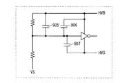
図1は、本実施形態に関するブートストラップ補償回路を例示する図である。
図4は、本実施形態に関するブートストラップ補償回路の動作を示すタイムチャートである。図4においては、基準電位VS、分圧電位取り出し点VMONの電位、および、出力回路611の出力信号の電位がそれぞれ例示される。なお、分圧電位取り出し点VMONの電位は、コンデンサ701を設けた場合が太線で示され、コンデンサ701を設けない場合が細線で示される。
本実施形態に関するブートストラップ補償回路およびパワーモジュールについて説明する。以下では、上記の実施形態で説明された構成と同様の構成については同じ符号を付して図示し、その詳細な説明については適宜省略する。
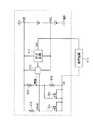
図5は、本実施形態に関するブートストラップ補償回路を例示する図である。
本実施形態に関するブートストラップ補償回路およびパワーモジュールについて説明する。以下では、上記の実施形態で説明された構成と同様の構成については同じ符号を付して図示し、その詳細な説明については適宜省略する。
図6に、本実施形態に関するブートストラップ補償回路を例示する図である。
本実施形態に関するブートストラップ補償回路およびパワーモジュールについて説明する。以下では、上記の実施形態で説明された構成と同様の構成については同じ符号を付して図示し、その詳細な説明については適宜省略する。
図8は、本実施形態に関するブートストラップ補償回路を例示する図である。
本実施形態に関するブートストラップ補償回路およびパワーモジュールについて説明する。以下では、上記の実施形態で説明された構成と同様の構成については同じ符号を付して図示し、その詳細な説明については適宜省略する。
図9は、本実施形態に関するブートストラップ補償回路を例示する図である。
本実施形態に関するブートストラップ補償回路およびパワーモジュールについて説明する。以下では、上記の実施形態で説明された構成と同様の構成については同じ符号を付して図示し、その詳細な説明については適宜省略する。
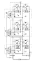
図10は、本実施形態に関する単相インバータを制御するパワーデバイス制御回路を例示する図である。図10に例示されるように、当該回路においては、MOSFET101と、MOSFET101のソース側にトーテムポール接続されたMOSFET102と、MOSFET103と、MOSFET103のソース側にトーテムポール接続されたMOSFET104と、MOSFET101のゲート電圧を制御するハイサイド制御回路201と、MOSFET102のゲート電圧を制御するローサイド制御回路202と、MOSFET103のゲート電圧を制御するハイサイド制御回路203と、MOSFET104のゲート電圧を制御するローサイド制御回路204と、ハイサイド制御回路201に接続されたブートストラップ回路401と、ハイサイド制御回路203に接続されたブートストラップ回路403と、ハイサイド制御回路201およびブートストラップ回路401に接続されたブートストラップ補償回路601と、ハイサイド制御回路203およびブートストラップ回路403に接続されたブートストラップ補償回路603とを備える。
以下に、上記の実施形態による効果を例示する。なお、以下では、上記の実施形態に例示された具体的な構成に基づく効果が記載されるが、同様の効果が生じる範囲で、本明細書に例示される他の具体的な構成と置き換えられてもよい。また、当該置き換えは、複数の実施形態に跨ってなされてもよい。すなわち、異なる実施形態において例示された各構成が組み合わされて、同様の効果が生じる場合であってもよい。
上記実施形態では、各構成要素の寸法、形状、相対的配置関係または実施の条件などについても記載する場合があるが、これらはすべての局面において例示であって、本明細書に記載されたものに限られることはない。よって、例示されていない無数の変形例が、本明細書に開示される技術の範囲内において想定される。たとえば、少なくとも1つの構成要素を変形する場合、追加する場合または省略する場合、さらには、少なくとも1つの実施形態における少なくとも1つの構成要素を抽出し、他の実施形態の構成要素と組み合わせる場合が含まれる。
Claims (9)
- ブートストラップ回路に電流を供給するブートストラップ補償回路であり、
前記ブートストラップ回路は、
高電圧側電位と低電圧側電位との間に高電圧側から順にトーテムポール接続されたハイサイドスイッチング素子およびローサイドスイッチング素子の駆動をそれぞれ制御するハイサイド制御回路およびローサイド制御回路のうちの、前記ハイサイド制御回路に電圧を供給するため、前記ハイサイドスイッチング素子と前記ローサイドスイッチング素子との接続点である基準電位と、前記ハイサイド制御回路との間に接続される第1コンデンサを備え、
前記ブートストラップ補償回路は、
前記高電圧側電位に対するフローティング電位と、前記基準電位との間に直列に接続される複数の抵抗と、
一端が、複数の前記抵抗の間の点である分圧電位取り出し点に接続され、他端が、前記基準電位に接続される第2コンデンサと、
前記分圧電位取り出し点の電位に基づいて、前記第1コンデンサに電流を供給する出力回路とを備える、
ブートストラップ補償回路。 - カソードが、前記フローティング電位に接続され、アノードが、前記分圧電位取り出し点に接続されるダイオードをさらに備える、
請求項1に記載のブートストラップ補償回路。 - カソードが、前記フローティング電位に接続され、アノードが、前記分圧電位取り出し点に接続されるツェナーダイオードをさらに備える、
請求項1に記載のブートストラップ補償回路。 - 請求項1から請求項3のうちのいずれか1項に記載のブートストラップ補償回路と、
前記ハイサイドスイッチング素子と、
前記ローサイドスイッチング素子と、
前記ハイサイド制御回路と、
前記ローサイド制御回路と、
前記ブートストラップ回路とを備える、
パワーモジュール。 - ブートストラップ回路に電流を供給するブートストラップ補償回路であり、
前記ブートストラップ回路は、
高電圧側電位と低電圧側電位との間に高電圧側から順にトーテムポール接続されたハイサイドスイッチング素子およびローサイドスイッチング素子の駆動をそれぞれ制御するハイサイド制御回路およびローサイド制御回路のうちの、前記ハイサイド制御回路に電圧を供給するため、前記ハイサイドスイッチング素子と前記ローサイドスイッチング素子との接続点である基準電位と、前記ハイサイド制御回路との間に接続されるコンデンサを備え、
前記ブートストラップ補償回路は、
前記高電圧側電位に対するフローティング電位と、前記基準電位との間に直列に接続される複数の第1抵抗と、
ドレインが、複数の前記第1抵抗の間の点である分圧電位取り出し点に接続され、ソースおよびゲートが、前記基準電位に接続される第1MOSFETと、
前記分圧電位取り出し点の電位に基づいて、前記コンデンサに電流を供給する出力回路とを備える、
ブートストラップ補償回路。 - 一端が、前記フローティング電位に接続される第2抵抗と、
ドレインが、前記第2抵抗の他端に接続される第2MOSFETと、
ドレインが、前記第2MOSFETのソースに接続され、ソースが、前記基準電位に接続される第3MOSFETとをさらに備え、
前記第1MOSFETのゲートと、前記第2MOSFETのゲートと、前記第3MOSFETのゲートとは、互いに接続され、
前記第2MOSFETのゲートと、前記第2MOSFETのソースとは、互いに接続される、
請求項5に記載のブートストラップ補償回路。 - カソードが、前記フローティング電位に接続され、アノードが、前記分圧電位取り出し点に接続されるダイオードをさらに備える、
請求項5または請求項6に記載のブートストラップ補償回路。 - カソードが、前記フローティング電位に接続され、アノードが、前記分圧電位取り出し点に接続されるツェナーダイオードをさらに備える、
請求項5または請求項6に記載のブートストラップ補償回路。 - 請求項5から請求項8のうちのいずれか1項に記載のブートストラップ補償回路と、
前記ハイサイドスイッチング素子と、
前記ローサイドスイッチング素子と、
前記ハイサイド制御回路と、
前記ローサイド制御回路と、
前記ブートストラップ回路とを備える、
パワーモジュール。
Priority Applications (4)
| Application Number | Priority Date | Filing Date | Title |
|---|---|---|---|
| JP2015177234A JP6370279B2 (ja) | 2015-09-09 | 2015-09-09 | ブートストラップ補償回路およびパワーモジュール |
| US15/130,164 US9755548B2 (en) | 2015-09-09 | 2016-04-15 | Bootstrap compensation circuit and power module |
| DE102016216993.9A DE102016216993A1 (de) | 2015-09-09 | 2016-09-07 | Bootstrap-Kompensierungsschaltung und Leistungsmodul |
| CN201610814823.7A CN106533129B (zh) | 2015-09-09 | 2016-09-09 | 自举补偿电路及功率模块 |
Applications Claiming Priority (1)
| Application Number | Priority Date | Filing Date | Title |
|---|---|---|---|
| JP2015177234A JP6370279B2 (ja) | 2015-09-09 | 2015-09-09 | ブートストラップ補償回路およびパワーモジュール |
Publications (3)
| Publication Number | Publication Date |
|---|---|
| JP2017055542A JP2017055542A (ja) | 2017-03-16 |
| JP2017055542A5 JP2017055542A5 (ja) | 2017-12-14 |
| JP6370279B2 true JP6370279B2 (ja) | 2018-08-08 |
Family
ID=58054828
Family Applications (1)
| Application Number | Title | Priority Date | Filing Date |
|---|---|---|---|
| JP2015177234A Active JP6370279B2 (ja) | 2015-09-09 | 2015-09-09 | ブートストラップ補償回路およびパワーモジュール |
Country Status (4)
| Country | Link |
|---|---|
| US (1) | US9755548B2 (ja) |
| JP (1) | JP6370279B2 (ja) |
| CN (1) | CN106533129B (ja) |
| DE (1) | DE102016216993A1 (ja) |
Families Citing this family (6)
| Publication number | Priority date | Publication date | Assignee | Title |
|---|---|---|---|---|
| WO2015187482A1 (en) * | 2014-06-03 | 2015-12-10 | Yale University | Bootstrapping circuit and unipolar logic circuits using the same |
| CN107437890B (zh) * | 2016-05-25 | 2020-09-01 | 松下知识产权经营株式会社 | 电力变换电路及电力传输系统 |
| US9966837B1 (en) | 2016-07-08 | 2018-05-08 | Vpt, Inc. | Power converter with circuits for providing gate driving |
| JP6784607B2 (ja) * | 2017-02-06 | 2020-11-11 | 株式会社京三製作所 | 絶縁電源、及び電力変換装置 |
| DE102019111996B3 (de) * | 2019-05-08 | 2020-07-09 | Webasto SE | Vorrichtung zur Ansteuerung von Halbleiter-Leistungsschaltern im Hochvoltbereich |
| CN110620493A (zh) * | 2019-10-25 | 2019-12-27 | 南京埃斯顿自动化股份有限公司 | 一种高位补能型自举电路及其控制方法 |
Family Cites Families (22)
| Publication number | Priority date | Publication date | Assignee | Title |
|---|---|---|---|---|
| US7301288B2 (en) * | 2004-04-08 | 2007-11-27 | International Rectifier Corporation | LED buck regulator control IC |
| US7145316B1 (en) * | 2005-06-06 | 2006-12-05 | Micrel, Inc. | Control circuit for monitoring and maintaining a bootstrap voltage in an N-channel buck regulator |
| ITMI20052051A1 (it) * | 2005-10-27 | 2007-04-28 | St Microelectronics Srl | Dispositivo di controllo di un convertitore a commutazione con circuito di protezione contro le sovraccorenti e relativo convertitore a commutazione |
| ITMI20052055A1 (it) * | 2005-10-27 | 2007-04-28 | St Microelectronics Srl | Dispositivo di controllo per un convertitore a commutazione e relativo convertitore a commutazione |
| US7911812B2 (en) * | 2007-01-22 | 2011-03-22 | Power Integrations, Inc. | Control arrangement for a PFC power converter |
| TWI371157B (en) * | 2008-11-19 | 2012-08-21 | Delta Electronics Inc | H-bridge circuit having energy compensation circuit and controlling method thereof |
| JP5359918B2 (ja) * | 2010-02-16 | 2013-12-04 | 三菱電機株式会社 | 半導体装置 |
| JP5499877B2 (ja) * | 2010-04-23 | 2014-05-21 | 三菱電機株式会社 | 電力用半導体装置 |
| JP2013062717A (ja) * | 2011-09-14 | 2013-04-04 | Mitsubishi Electric Corp | 半導体装置 |
| JP5910395B2 (ja) * | 2011-09-16 | 2016-04-27 | サンケン電気株式会社 | ドライブ回路 |
| CN103023469B (zh) * | 2011-09-23 | 2015-12-02 | 国民技术股份有限公司 | 一种栅压自举开关电路 |
| US9048747B2 (en) * | 2011-11-23 | 2015-06-02 | Zahid Ansari | Switched-mode power supply startup circuit, method, and system incorporating same |
| US9479055B2 (en) * | 2012-12-03 | 2016-10-25 | Panasonic Intellectual Property Management Co., Ltd. | DC-DC converter |
| JP2014147189A (ja) * | 2013-01-28 | 2014-08-14 | Fuji Electric Co Ltd | 電力変換装置の駆動回路 |
| JPWO2014119307A1 (ja) * | 2013-01-31 | 2017-01-26 | パナソニックIpマネジメント株式会社 | Dc/dcコンバータ |
| TWM472362U (zh) * | 2013-08-07 | 2014-02-11 | Richtek Technology Corp | 降壓型切換式電源供應器 |
| JP6065808B2 (ja) * | 2013-10-24 | 2017-01-25 | 三菱電機株式会社 | 半導体装置及び半導体モジュール |
| US9647476B2 (en) * | 2014-09-16 | 2017-05-09 | Navitas Semiconductor Inc. | Integrated bias supply, reference and bias current circuits for GaN devices |
| US9571093B2 (en) * | 2014-09-16 | 2017-02-14 | Navitas Semiconductor, Inc. | Half bridge driver circuits |
| CN110429804A (zh) * | 2014-10-24 | 2019-11-08 | 意法半导体研发(深圳)有限公司 | 反相升降压型变换器驱动电路和方法 |
| US9270177B1 (en) * | 2014-11-20 | 2016-02-23 | Sanken Electric Co., Ltd. | Switching power-supply device |
| US9577505B1 (en) * | 2015-07-28 | 2017-02-21 | Dell Products L.P. | Bootstrap controller for switching power supply |
-
2015
- 2015-09-09 JP JP2015177234A patent/JP6370279B2/ja active Active
-
2016
- 2016-04-15 US US15/130,164 patent/US9755548B2/en active Active
- 2016-09-07 DE DE102016216993.9A patent/DE102016216993A1/de active Pending
- 2016-09-09 CN CN201610814823.7A patent/CN106533129B/zh active Active
Also Published As
| Publication number | Publication date |
|---|---|
| CN106533129A (zh) | 2017-03-22 |
| US20170070220A1 (en) | 2017-03-09 |
| JP2017055542A (ja) | 2017-03-16 |
| US9755548B2 (en) | 2017-09-05 |
| CN106533129B (zh) | 2019-06-21 |
| DE102016216993A1 (de) | 2017-03-09 |
Similar Documents
| Publication | Publication Date | Title |
|---|---|---|
| JP6370279B2 (ja) | ブートストラップ補償回路およびパワーモジュール | |
| JP6209205B2 (ja) | GaNFETのゲートの保護のためのドライバ回路のためのシステム及び装置 | |
| US20190393871A1 (en) | Cascode switches including normally-off and normally-on devices and circuits comprising the switches | |
| KR101062265B1 (ko) | 강압형 스위칭 레귤레이터 | |
| JP5315026B2 (ja) | 半導体装置 | |
| JP5934925B2 (ja) | ゲートドライバおよびこれを備えたパワーモジュール | |
| CN107980199B (zh) | 电源开关装置 | |
| US20140285241A1 (en) | Driver circuit | |
| JP5488550B2 (ja) | ゲート駆動回路および電力変換装置 | |
| US20110080205A1 (en) | Switch Driving Circuit And Driving Method Thereof | |
| JP2011234430A (ja) | 電力用半導体装置 | |
| KR20150071339A (ko) | 게이트 구동 회로 | |
| JP6323834B2 (ja) | 同期整流装置およびこれを用いたオルタネータ | |
| US10715027B2 (en) | Driver circuit | |
| CN105575960B (zh) | 用于芯片上静电放电保护方案的方法及电路 | |
| JP2015080335A (ja) | ゲート駆動回路 | |
| JP2009075957A (ja) | 電源回路および半導体装置 | |
| CN105991052B (zh) | 具有减小的反向恢复时间的整流器电路 | |
| JP2012205356A (ja) | 整流スイッチユニット、整流回路及びスイッチング電源装置 | |
| JP2018074676A (ja) | ゲート駆動回路 | |
| JP2021150532A (ja) | 半導体装置 | |
| JP2020096444A (ja) | スイッチング回路 | |
| JP2009095166A (ja) | 電圧制御形スイッチングデバイスのゲート駆動装置 | |
| JP5226474B2 (ja) | 半導体出力回路 | |
| JP2021082879A (ja) | 論理回路および回路チップ |
Legal Events
| Date | Code | Title | Description |
|---|---|---|---|
| A521 | Request for written amendment filed |
Free format text: JAPANESE INTERMEDIATE CODE: A523 Effective date: 20171101 |
|
| A621 | Written request for application examination |
Free format text: JAPANESE INTERMEDIATE CODE: A621 Effective date: 20171101 |
|
| TRDD | Decision of grant or rejection written | ||
| A01 | Written decision to grant a patent or to grant a registration (utility model) |
Free format text: JAPANESE INTERMEDIATE CODE: A01 Effective date: 20180612 |
|
| A977 | Report on retrieval |
Free format text: JAPANESE INTERMEDIATE CODE: A971007 Effective date: 20180613 |
|
| A61 | First payment of annual fees (during grant procedure) |
Free format text: JAPANESE INTERMEDIATE CODE: A61 Effective date: 20180710 |
|
| R150 | Certificate of patent or registration of utility model |
Ref document number: 6370279 Country of ref document: JP Free format text: JAPANESE INTERMEDIATE CODE: R150 |
|
| R250 | Receipt of annual fees |
Free format text: JAPANESE INTERMEDIATE CODE: R250 |
|
| R250 | Receipt of annual fees |
Free format text: JAPANESE INTERMEDIATE CODE: R250 |
|
| R250 | Receipt of annual fees |
Free format text: JAPANESE INTERMEDIATE CODE: R250 |