JP6233033B2 - 半導体装置の製造方法 - Google Patents
半導体装置の製造方法 Download PDFInfo
- Publication number
- JP6233033B2 JP6233033B2 JP2014004253A JP2014004253A JP6233033B2 JP 6233033 B2 JP6233033 B2 JP 6233033B2 JP 2014004253 A JP2014004253 A JP 2014004253A JP 2014004253 A JP2014004253 A JP 2014004253A JP 6233033 B2 JP6233033 B2 JP 6233033B2
- Authority
- JP
- Japan
- Prior art keywords
- silicon oxide
- oxide film
- film
- polysilicon film
- semiconductor device
- Prior art date
- Legal status (The legal status is an assumption and is not a legal conclusion. Google has not performed a legal analysis and makes no representation as to the accuracy of the status listed.)
- Active
Links
Images


Landscapes
- Bipolar Transistors (AREA)
Description
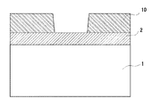
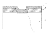
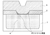
本発明の実施の形態1に係る半導体装置の製造方法について、図1から図8を参照して説明する。
Claims (3)
- 不純物拡散領域を有する半導体装置の製造方法であって、
シリコン基板上に第一のシリコン酸化膜を形成する工程と、
不純物拡散領域を形成するシリコン基板上の前記第一のシリコン酸化膜を除去する工程と、
前記シリコン基板上および前記第一のシリコン酸化膜上に不純物が導入されたポリシリコン膜を形成する工程と、
熱酸化処理により前記ポリシリコン膜を所定の膜厚を残して第二のシリコン酸化膜にすると同時に、前記ポリシリコン膜中の不純物を前記シリコン基板中に拡散させる工程と、
前記ポリシリコン膜上に形成された前記第二のシリコン酸化膜を除去する工程と、
残された前記ポリシリコン膜を熱酸化処理により第三のシリコン酸化膜にする工程と、
シリコン基板上の前記第三のシリコン酸化膜および前記第一のシリコン酸化膜を一度に除去する工程とを含むことを特徴とする半導体装置の製造方法。 - 前記ポリシリコン膜を第二のシリコン酸化膜にする工程において、残される前記ポリシリコン膜の所定の膜厚を100nmとすることを特徴とする請求項1記載の半導体装置の製造方法。
- 前記ポリシリコン膜は、その形成時の膜厚が200nm以上で、かつその不純物濃度が5.0×10²⁰/cm3以上のリンが導入されていることを特徴とする請求項1または請求項2に記載の半導体装置の製造方法。
Priority Applications (1)
| Application Number | Priority Date | Filing Date | Title |
|---|---|---|---|
| JP2014004253A JP6233033B2 (ja) | 2014-01-14 | 2014-01-14 | 半導体装置の製造方法 |
Applications Claiming Priority (1)
| Application Number | Priority Date | Filing Date | Title |
|---|---|---|---|
| JP2014004253A JP6233033B2 (ja) | 2014-01-14 | 2014-01-14 | 半導体装置の製造方法 |
Publications (2)
| Publication Number | Publication Date |
|---|---|
| JP2015133412A JP2015133412A (ja) | 2015-07-23 |
| JP6233033B2 true JP6233033B2 (ja) | 2017-11-22 |
Family
ID=53900407
Family Applications (1)
| Application Number | Title | Priority Date | Filing Date |
|---|---|---|---|
| JP2014004253A Active JP6233033B2 (ja) | 2014-01-14 | 2014-01-14 | 半導体装置の製造方法 |
Country Status (1)
| Country | Link |
|---|---|
| JP (1) | JP6233033B2 (ja) |
Family Cites Families (5)
| Publication number | Priority date | Publication date | Assignee | Title |
|---|---|---|---|---|
| JPS55151332A (en) * | 1979-05-14 | 1980-11-25 | Pioneer Electronic Corp | Fabricating method of semiconductor device |
| JPS571226A (en) * | 1980-06-03 | 1982-01-06 | Nippon Telegr & Teleph Corp <Ntt> | Manufacture of semiconductor substrate with buried diffusion layer |
| JPS58184738A (ja) * | 1982-03-30 | 1983-10-28 | レイセオン カンパニ− | 半導体製造方法 |
| JPH0233932A (ja) * | 1988-07-23 | 1990-02-05 | Nec Corp | 半導体装置の製造方法 |
| JP2008066436A (ja) * | 2006-09-06 | 2008-03-21 | Yokogawa Electric Corp | 半導体素子とその製造方法 |
-
2014
- 2014-01-14 JP JP2014004253A patent/JP6233033B2/ja active Active
Also Published As
| Publication number | Publication date |
|---|---|
| JP2015133412A (ja) | 2015-07-23 |
Similar Documents
| Publication | Publication Date | Title |
|---|---|---|
| JP4825402B2 (ja) | 半導体装置の製造方法 | |
| JPH10209168A (ja) | 半導体装置の製造方法 | |
| JP2006108646A (ja) | 半導体装置及びその製造方法 | |
| JP2006269551A (ja) | 半導体装置及びその製造方法 | |
| JP6233033B2 (ja) | 半導体装置の製造方法 | |
| JP5723483B2 (ja) | 半導体装置の製造方法 | |
| JP3575408B2 (ja) | トレンチ素子分離領域を有する半導体装置の製造方法 | |
| JP6413938B2 (ja) | 半導体基板の評価方法 | |
| JP2009252842A (ja) | 半導体装置及びその製造方法 | |
| JP2010050145A (ja) | 素子分離構造の製造方法および素子分離構造 | |
| JP2007103492A (ja) | 半導体装置の製造方法及び半導体装置 | |
| JPH088262A (ja) | 半導体装置の製造方法 | |
| CN108630605B (zh) | 半导体装置及其制造方法 | |
| JP5003857B2 (ja) | 半導体装置の製造方法 | |
| JP2006294959A (ja) | 半導体装置の製造方法及び半導体基板 | |
| JP2008047691A (ja) | 半導体装置の製法 | |
| JP2763216B2 (ja) | 半導体装置の製造方法 | |
| JP2021064747A (ja) | 半導体装置の製造方法 | |
| JP2010098152A (ja) | 半導体装置の製造方法 | |
| JP2010109049A (ja) | 半導体装置の製造方法 | |
| JP2010028008A (ja) | 半導体装置の製造方法 | |
| JP5245327B2 (ja) | 半導体装置の製造方法 | |
| JP5458547B2 (ja) | 半導体装置の製造方法 | |
| JP2006093185A (ja) | メサ型半導体装置の製造方法 | |
| KR20090123692A (ko) | 반도체 소자의 제조방법 |
Legal Events
| Date | Code | Title | Description |
|---|---|---|---|
| A621 | Written request for application examination |
Free format text: JAPANESE INTERMEDIATE CODE: A621 Effective date: 20160520 |
|
| A977 | Report on retrieval |
Free format text: JAPANESE INTERMEDIATE CODE: A971007 Effective date: 20170206 |
|
| A131 | Notification of reasons for refusal |
Free format text: JAPANESE INTERMEDIATE CODE: A131 Effective date: 20170214 |
|
| TRDD | Decision of grant or rejection written | ||
| A01 | Written decision to grant a patent or to grant a registration (utility model) |
Free format text: JAPANESE INTERMEDIATE CODE: A01 Effective date: 20170926 |
|
| A61 | First payment of annual fees (during grant procedure) |
Free format text: JAPANESE INTERMEDIATE CODE: A61 Effective date: 20171009 |
|
| R151 | Written notification of patent or utility model registration |
Ref document number: 6233033 Country of ref document: JP Free format text: JAPANESE INTERMEDIATE CODE: R151 |
|
| R250 | Receipt of annual fees |
Free format text: JAPANESE INTERMEDIATE CODE: R250 |
|
| R250 | Receipt of annual fees |
Free format text: JAPANESE INTERMEDIATE CODE: R250 |
|
| R250 | Receipt of annual fees |
Free format text: JAPANESE INTERMEDIATE CODE: R250 |
|
| R250 | Receipt of annual fees |
Free format text: JAPANESE INTERMEDIATE CODE: R250 |