JP6233033B2 - Manufacturing method of semiconductor device - Google Patents
Manufacturing method of semiconductor device Download PDFInfo
- Publication number
- JP6233033B2 JP6233033B2 JP2014004253A JP2014004253A JP6233033B2 JP 6233033 B2 JP6233033 B2 JP 6233033B2 JP 2014004253 A JP2014004253 A JP 2014004253A JP 2014004253 A JP2014004253 A JP 2014004253A JP 6233033 B2 JP6233033 B2 JP 6233033B2
- Authority
- JP
- Japan
- Prior art keywords
- silicon oxide
- oxide film
- film
- polysilicon film
- semiconductor device
- Prior art date
- Legal status (The legal status is an assumption and is not a legal conclusion. Google has not performed a legal analysis and makes no representation as to the accuracy of the status listed.)
- Active
Links
Images


Landscapes
- Bipolar Transistors (AREA)
Description
本発明は、半導体装置の製造方法に関して、特に半導体装置における所定の領域に高濃度の不純物拡散領域を形成する方法に関する。 The present invention relates to a method for manufacturing a semiconductor device, and more particularly to a method for forming a high concentration impurity diffusion region in a predetermined region in a semiconductor device.
従来の半導体装置の製造方法においては、不純物が導入されたポリシリコン膜を、シリコン酸化膜がマスクとして表面に設けられたシリコン基板上に成膜し、このポリシリコン膜を熱酸化する過程で不純物をシリコン基板に導入した後、マスクと共に除去することで、同基板内に不純物拡散領域を形成する技術があった。そしてこの方法は、バイポーラトランジスタの埋め込みコレクタ層の形成に適用されている(たとえば、特許文献1参照)。 In a conventional method for manufacturing a semiconductor device, a polysilicon film into which an impurity has been introduced is formed on a silicon substrate provided on the surface using a silicon oxide film as a mask, and the polysilicon film is subjected to thermal oxidation in the process of thermal oxidation. There is a technique for forming an impurity diffusion region in the substrate by removing it together with the mask after introducing it into the silicon substrate. This method is applied to the formation of a buried collector layer of a bipolar transistor (see, for example, Patent Document 1).
従来の半導体装置の製造方法では、例えば、バイポーラトランジスタのコレクタウォール領域などで必要とされる表面部において1.0×10¹⁹〜1.0×10²⁰/cm3の高濃度で、かつ10μm以上と深い不純物拡散領域を形成しようとした場合、成膜されるポリシリコン膜の膜厚を厚くする必要がある。しかしながらこの場合熱酸化の過程で形成されるシリコン酸化膜の膜厚も厚くなることから、次第に形成されたシリコン酸化膜とポリシリコン膜との界面に酸化種が到達し難くなる。 In the conventional method for manufacturing a semiconductor device, for example, a high concentration of 1.0 × 10 19 to 1.0 × 10 20 / cm 3 and 10 μm or more in a surface portion required for a collector wall region of a bipolar transistor or the like. When a deep impurity diffusion region is to be formed, it is necessary to increase the thickness of the polysilicon film to be formed. However, in this case, since the thickness of the silicon oxide film formed in the process of thermal oxidation is also increased, it is difficult for the oxidized species to reach the interface between the silicon oxide film and the polysilicon film formed gradually.
したがって、特に不純物拡散のマスクとして使用するシリコン酸化膜の開口部に生じる段差部ではポリシリコン膜の厚みが平坦部より大きくなるため、マスクの開口部であるシリコン酸化膜端部とポリシリコン膜、そしてシリコン基板との界面付近において、ポリシリコン膜が部分的に酸化されずにポリシリコン膜のまま一部が残る場合があった(図9参照)。 Therefore, since the thickness of the polysilicon film is larger than the flat portion in the step portion generated in the opening portion of the silicon oxide film used as a mask for impurity diffusion in particular, the end portion of the silicon oxide film that is the opening portion of the mask, In the vicinity of the interface with the silicon substrate, the polysilicon film is not partially oxidized and a part of the polysilicon film may remain (see FIG. 9).
このような場合、このポリシリコン膜の残渣がエッチング加工等によりシリコン酸化膜を除去する際、発塵源となる可能性があった。 In such a case, the residue of the polysilicon film may become a dust generation source when the silicon oxide film is removed by etching or the like.
この発塵を回避するための方法として、熱酸化処理を長時間行うことでポリシリコン膜の残渣が生じないようにすることも可能であるが、過剰な熱酸化により、シリコン酸化膜およびシリコン酸化膜の界面付近のシリコン基板に局所的に応力が発生し、リーク電流不良などのデバイス特性不良を引き起こす場合があった。 As a method for avoiding this dust generation, it is possible to prevent the residue of the polysilicon film from being generated by performing the thermal oxidation process for a long time. However, excessive thermal oxidation causes the silicon oxide film and the silicon oxide to remain. In some cases, stress is locally generated in the silicon substrate near the interface of the film, causing a device characteristic failure such as a leakage current failure.
本発明は上述のような課題を解決するためになされたもので、ポリシリコン残渣の発生を無くすとともに、デバイス特性不良の要因となり得る局所的に発生する応力を抑制することのできる半導体装置の製造方法を提供することを目的とする。 SUMMARY OF THE INVENTION The present invention has been made to solve the above-described problems, and the manufacture of a semiconductor device capable of eliminating the generation of polysilicon residues and suppressing locally generated stress that may cause device characteristic defects. It aims to provide a method.
本発明に係る半導体装置の製造方法は、シリコン基板上に第一のシリコン酸化膜を形成する工程と、不純物拡散領域を形成するシリコン基板上の第一のシリコン酸化膜を除去する工程と、シリコン基板上および第一のシリコン酸化膜上に不純物が導入されたポリシリコン膜を形成する工程と、熱処理によりポリシリコン膜を所定の膜厚を残して第二のシリコン酸化膜にすると同時に、ポリシリコン膜中の不純物をシリコン基板中に拡散させる工程と、ポリシリコン膜上に形成された第二のシリコン酸化膜を除去する工程と、残されたポリシリコン膜を熱処理により第三のシリコン酸化膜にする工程と、シリコン基板上に形成された第一と第三のシリコン酸化膜を除去する工程とを含むことを特徴とするものである。 A method of manufacturing a semiconductor device according to the present invention includes a step of forming a first silicon oxide film on a silicon substrate, a step of removing the first silicon oxide film on the silicon substrate on which an impurity diffusion region is to be formed, and silicon A step of forming a polysilicon film doped with impurities on the substrate and the first silicon oxide film; and a heat treatment to leave the polysilicon film to a second silicon oxide film while leaving a predetermined film thickness; The step of diffusing impurities in the film into the silicon substrate, the step of removing the second silicon oxide film formed on the polysilicon film, and the remaining polysilicon film by heat treatment into a third silicon oxide film And a step of removing the first and third silicon oxide films formed on the silicon substrate.
本発明は。不純物の拡散源となるポリシリコン膜を2回に分けて熱酸化処理することにより、発塵源となり得るポリシリコン残渣を無くし、且つデバイス特性不良の要因となり得る応力の発生を緩和することができる。 The present invention. By subjecting the polysilicon film, which is an impurity diffusion source, to thermal oxidation in two steps, it is possible to eliminate polysilicon residues that can be a dust generation source and to reduce the generation of stress that can cause device characteristic defects. .
実施の形態1.
本発明の実施の形態1に係る半導体装置の製造方法について、図1から図8を参照して説明する。
A method for manufacturing a semiconductor device according to the first embodiment of the present invention will be described with reference to FIGS.
本発明の実施の形態1における不純物拡散領域は、バイポーラトランジスタのコレクタウォール領域の形成について説明するものとし、その表面部における不純物濃度は1.0×10¹⁹〜1.0×10²⁰/cm3で、深さ10μm以上のN型不純物拡散領域を形成するものとする。 The impurity diffusion region in the first embodiment of the present invention will be described with reference to the formation of the collector wall region of the bipolar transistor, and the impurity concentration in the surface portion is 1.0 × 10 19 to 1.0 × 10 20 / cm 3. Thus, an N-type impurity diffusion region having a depth of 10 μm or more is formed.
まず、図1に示すようにシリコン基板1に1000℃程度の温度で熱酸化処理(ウエット酸化の場合で、約3時間)を施すことで、シリコン基板1の表面に厚さ500nmの第一のシリコン酸化膜2を形成する。なお、シリコン基板1はN型でその不純物濃度は3.0×10¹⁵/cm3(比抵抗1.5Ω-cm)であり、これはエピタキシャル層の場合であってもよい。
First, as shown in FIG. 1, the
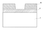
次に、形成する不純物拡散領域上の第一のシリコン酸化膜2の一部分を除去するため、写真製版処理により図2に示すように第一のシリコン酸化膜2上にレジストマスク10を形成する。
Next, in order to remove a part of the first
次に、図3に示すようにドライエッチング処理を施し、レジストマスク10がない部分の第一のシリコン酸化膜2を除去して、シリコン基板1の表面を露出(A0)させる。
Next, as shown in FIG. 3, a dry etching process is performed to remove the portion of the first
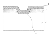
次に、レジストマスク10を除去して後、図4に示すように第一のシリコン酸化膜2上および第一のシリコン酸化膜2が除去されたシリコン基板1上に、例えばCVD法によって厚さ200nmのポリシリコン膜3を形成し、これに高濃度(5.0×10²⁰〜6.5×10²⁰/cm3程度)のリンを導入するためのイオン注入を行う。高濃度のリンが導入されたポリシリコン膜3は、不純物拡散領域形成における拡散源となる。
Next, after removing the
なお、ポリシリコン膜3中への不純物の導入に関しては、CVD法による膜形成時に不純物をドーピングガスとして添加・反応させる方法でも導入可能である。また、不純物拡散領域の濃度、あるいは深さについてその値を更に大きくする必要がある場合は、ポリシリコン膜3の膜厚を厚くすることにより対応が可能となる。
The introduction of impurities into the
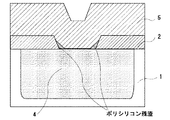
次に、第一のシリコン酸化膜2およびリンが導入されたポリシリコン膜3が形成されたシリコン基板1は1000℃程度の温度で熱酸化処理(ウエット酸化の場合で、約15分)を施す。この処理によって、図5に示すように、ポリシリコン膜3の上面部より酸化されて第二のシリコン酸化膜5が形成されると同時に、ポリシリコン膜3中のリンがポリシリコン膜3とシリコン基板1との界面部を通してシリコン基板1に拡散され、N型不純物拡散領域4が形成される。
Next, the
そして、この熱酸化処理によりポリシリコン膜3の膜厚は時間と共に薄くなるが、熱酸化処理はポリシリコン膜3の厚さが100nm 程度になった時点で、一旦を終了する。
The thermal oxidation process reduces the thickness of the
またこのとき、ポリシリコン膜3が酸化されたことにより表面に形成された第二のシリコン酸化膜5は、270nm程度の厚さになっている。
At this time, the second
次に、表面に形成された第二のシリコン酸化膜5を、例えばウエットエッチング処理により図6に示すように除去する。この際、フッ酸等のエッチング剤がポリシリコン膜3のピンホール等から漏れることで、第一のシリコン酸化膜2も同時に除去されることを防止する必要がある。そのためには、熱酸化をされずに残されるポリシリコン膜3の厚さとして、100nm程度が良好な膜質と制御性の良さなどから最適となる。
Next, the second
すなわち、ポリシリコン膜3の厚さが100nmを下回って80nm以下の厚さとなるとピンホールを生じる可能性が高くなる。
In other words, if the thickness of the
次に図7に示すように、再び1000℃程度の温度で熱酸化処理(ウエット酸化の場合で、約2時間)し、ポリシリコン膜3を酸化種と反応させることでシリコン酸化膜を形成する。この工程によって、ポリシリコン膜3はすべて第三のシリコン酸化膜6に置換される。
Next, as shown in FIG. 7, a thermal oxidation process is again performed at a temperature of about 1000 ° C. (about 2 hours in the case of wet oxidation), and the
ここで、再び熱酸化処理を施す最初の状態においては、ポリシリコン膜3上にはシリコン酸化膜が無く、またこのポリシリコン膜3の膜厚を100nm程度としていることで、ポリシリコン膜3がすべて第三のシリコン酸化膜6に置換されるまでの過程においても、酸化種がポリシリコン膜3へ到達し易い状態が継続されることになる。そのため、従来技術における図9に示すようなポリシリコン膜の残渣が生じることはない。そのことによって、過剰な熱酸化を施す必要がなくなるので、シリコン酸化膜およびシリコン酸化膜の界面付近のシリコン基板において局所的な応力の発生も抑えられ、これを原因とするリーク電流などのデバイス特性への悪影響も抑制することができる。
Here, in the initial state in which the thermal oxidation process is performed again, there is no silicon oxide film on the
その後、図8に示すように、第三のシリコン酸化膜6および第二のシリコン酸化膜2を、例えばウエットエッチング処理により一度に除去する。
Thereafter, as shown in FIG. 8, the third silicon oxide film 6 and the second
以上の工程を経ることにより、表面部の不純物濃度が1.0×10¹⁹〜1.0×10²⁰/cm3で、かつ深さ約10μmのバイポーラトランジスタのコレクタウォール領域として機能するN型不純物拡散領域4が形成される。
Through the above steps, an N-type impurity which functions as a collector wall region of a bipolar transistor having a surface portion impurity concentration of 1.0 × 10 19 to 1.0 × 10 20 / cm 3 and a depth of about 10 μm. A
なお、本発明の実施の形態では、不純物拡散のマスクとして熱酸化処理によるシリコン酸化膜を用いたが、CVD法により形成してもよい。また、同シリコン酸化膜に替えてシリコン窒化膜を使用することも可能である。 In the embodiment of the present invention, a silicon oxide film by thermal oxidation is used as a mask for impurity diffusion, but it may be formed by a CVD method. It is also possible to use a silicon nitride film instead of the silicon oxide film.
1 シリコン基板、2 第一のシリコン酸化膜、3 高濃度のリンが導入されたポリシリコン膜、4 N型不純物拡散領域、5 第二のシリコン酸化膜、6 第三のシリコン酸化膜
DESCRIPTION OF
Claims (3)
シリコン基板上に第一のシリコン酸化膜を形成する工程と、
不純物拡散領域を形成するシリコン基板上の前記第一のシリコン酸化膜を除去する工程と、
前記シリコン基板上および前記第一のシリコン酸化膜上に不純物が導入されたポリシリコン膜を形成する工程と、
熱酸化処理により前記ポリシリコン膜を所定の膜厚を残して第二のシリコン酸化膜にすると同時に、前記ポリシリコン膜中の不純物を前記シリコン基板中に拡散させる工程と、
前記ポリシリコン膜上に形成された前記第二のシリコン酸化膜を除去する工程と、
残された前記ポリシリコン膜を熱酸化処理により第三のシリコン酸化膜にする工程と、
シリコン基板上の前記第三のシリコン酸化膜および前記第一のシリコン酸化膜を一度に除去する工程とを含むことを特徴とする半導体装置の製造方法。 A method of manufacturing a semiconductor device having an impurity diffusion region,
Forming a first silicon oxide film on the silicon substrate;
Removing the first silicon oxide film on the silicon substrate forming the impurity diffusion region;
Forming a polysilicon film doped with impurities on the silicon substrate and the first silicon oxide film;
A step of diffusing impurities in the polysilicon film into the silicon substrate at the same time as making the polysilicon film a second silicon oxide film leaving a predetermined film thickness by thermal oxidation treatment;
Removing the second silicon oxide film formed on the polysilicon film;
A step of converting the remaining polysilicon film into a third silicon oxide film by thermal oxidation;
And a step of removing the third silicon oxide film and the first silicon oxide film on the silicon substrate at a time.
Priority Applications (1)
| Application Number | Priority Date | Filing Date | Title |
|---|---|---|---|
| JP2014004253A JP6233033B2 (en) | 2014-01-14 | 2014-01-14 | Manufacturing method of semiconductor device |
Applications Claiming Priority (1)
| Application Number | Priority Date | Filing Date | Title |
|---|---|---|---|
| JP2014004253A JP6233033B2 (en) | 2014-01-14 | 2014-01-14 | Manufacturing method of semiconductor device |
Publications (2)
| Publication Number | Publication Date |
|---|---|
| JP2015133412A JP2015133412A (en) | 2015-07-23 |
| JP6233033B2 true JP6233033B2 (en) | 2017-11-22 |
Family
ID=53900407
Family Applications (1)
| Application Number | Title | Priority Date | Filing Date |
|---|---|---|---|
| JP2014004253A Active JP6233033B2 (en) | 2014-01-14 | 2014-01-14 | Manufacturing method of semiconductor device |
Country Status (1)
| Country | Link |
|---|---|
| JP (1) | JP6233033B2 (en) |
Family Cites Families (5)
| Publication number | Priority date | Publication date | Assignee | Title |
|---|---|---|---|---|
| JPS55151332A (en) * | 1979-05-14 | 1980-11-25 | Pioneer Electronic Corp | Fabricating method of semiconductor device |
| JPS571226A (en) * | 1980-06-03 | 1982-01-06 | Nippon Telegr & Teleph Corp <Ntt> | Manufacture of semiconductor substrate with buried diffusion layer |
| JPS58184738A (en) * | 1982-03-30 | 1983-10-28 | レイセオン カンパニ− | Method of producing semiconductor |
| JPH0233932A (en) * | 1988-07-23 | 1990-02-05 | Nec Corp | Manufacture of semiconductor device |
| JP2008066436A (en) * | 2006-09-06 | 2008-03-21 | Yokogawa Electric Corp | Semiconductor device and manufacturing method thereof |
-
2014
- 2014-01-14 JP JP2014004253A patent/JP6233033B2/en active Active
Also Published As
| Publication number | Publication date |
|---|---|
| JP2015133412A (en) | 2015-07-23 |
Similar Documents
| Publication | Publication Date | Title |
|---|---|---|
| JP4825402B2 (en) | Manufacturing method of semiconductor device | |
| JPH10209168A (en) | Manufacture of semiconductor device | |
| JP2006108646A (en) | Semiconductor device and method of manufacturing the same | |
| JP2006269551A (en) | Semiconductor device and its manufacturing method | |
| JP6233033B2 (en) | Manufacturing method of semiconductor device | |
| JP5723483B2 (en) | Manufacturing method of semiconductor device | |
| JP3575408B2 (en) | Method of manufacturing semiconductor device having trench element isolation region | |
| JP6413938B2 (en) | Semiconductor substrate evaluation method | |
| JP2009252842A (en) | Semiconductor device and method of manufacturing the same | |
| JP2010050145A (en) | Method for manufacturing element isolation structure, and element isolation structure | |
| JP2007103492A (en) | Semiconductor device and manufacturing method thereof | |
| JPH088262A (en) | Manufacture of semiconductor device | |
| CN108630605B (en) | Semiconductor device and method for manufacturing the same | |
| JP5003857B2 (en) | Manufacturing method of semiconductor device | |
| JP2006294959A (en) | Process for fabricating semiconductor device and semiconductor substrate | |
| JP2008047691A (en) | Semiconductor device manufacturing method | |
| JP2763216B2 (en) | Method for manufacturing semiconductor device | |
| JP2021064747A (en) | Manufacturing method of semiconductor device | |
| JP2010109049A (en) | Method of manufacturing semiconductor device | |
| JP2010028008A (en) | Method for manufacturing semiconductor device | |
| JP5245327B2 (en) | Manufacturing method of semiconductor device | |
| JP5458547B2 (en) | Manufacturing method of semiconductor device | |
| JP2009123861A (en) | Method of manufacturing epitaxial wafer | |
| JP2006093185A (en) | Mesa semiconductor device manufacturing method | |
| KR20090123692A (en) | Method for manufacturing semiconductor device |
Legal Events
| Date | Code | Title | Description |
|---|---|---|---|
| A621 | Written request for application examination |
Free format text: JAPANESE INTERMEDIATE CODE: A621 Effective date: 20160520 |
|
| A977 | Report on retrieval |
Free format text: JAPANESE INTERMEDIATE CODE: A971007 Effective date: 20170206 |
|
| A131 | Notification of reasons for refusal |
Free format text: JAPANESE INTERMEDIATE CODE: A131 Effective date: 20170214 |
|
| TRDD | Decision of grant or rejection written | ||
| A01 | Written decision to grant a patent or to grant a registration (utility model) |
Free format text: JAPANESE INTERMEDIATE CODE: A01 Effective date: 20170926 |
|
| A61 | First payment of annual fees (during grant procedure) |
Free format text: JAPANESE INTERMEDIATE CODE: A61 Effective date: 20171009 |
|
| R151 | Written notification of patent or utility model registration |
Ref document number: 6233033 Country of ref document: JP Free format text: JAPANESE INTERMEDIATE CODE: R151 |
|
| R250 | Receipt of annual fees |
Free format text: JAPANESE INTERMEDIATE CODE: R250 |
|
| R250 | Receipt of annual fees |
Free format text: JAPANESE INTERMEDIATE CODE: R250 |
|
| R250 | Receipt of annual fees |
Free format text: JAPANESE INTERMEDIATE CODE: R250 |
|
| R250 | Receipt of annual fees |
Free format text: JAPANESE INTERMEDIATE CODE: R250 |