JP6228381B2 - 半導体装置 - Google Patents
半導体装置 Download PDFInfo
- Publication number
- JP6228381B2 JP6228381B2 JP2013092167A JP2013092167A JP6228381B2 JP 6228381 B2 JP6228381 B2 JP 6228381B2 JP 2013092167 A JP2013092167 A JP 2013092167A JP 2013092167 A JP2013092167 A JP 2013092167A JP 6228381 B2 JP6228381 B2 JP 6228381B2
- Authority
- JP
- Japan
- Prior art keywords
- configuration data
- transistor
- function
- data
- memory
- Prior art date
- Legal status (The legal status is an assumption and is not a legal conclusion. Google has not performed a legal analysis and makes no representation as to the accuracy of the status listed.)
- Expired - Fee Related
Links
- 239000004065 semiconductor Substances 0.000 title claims description 97
- 230000006870 function Effects 0.000 claims description 68
- 238000003860 storage Methods 0.000 claims description 68
- 239000003990 capacitor Substances 0.000 claims description 31
- 230000015572 biosynthetic process Effects 0.000 claims description 20
- 229910052733 gallium Inorganic materials 0.000 claims description 5
- 229910052738 indium Inorganic materials 0.000 claims description 5
- 229910052725 zinc Inorganic materials 0.000 claims description 4
- 239000011701 zinc Substances 0.000 description 34
- 239000013078 crystal Substances 0.000 description 31
- 238000012545 processing Methods 0.000 description 21
- 238000000034 method Methods 0.000 description 15
- 229910052710 silicon Inorganic materials 0.000 description 11
- 239000010703 silicon Substances 0.000 description 11
- 238000010586 diagram Methods 0.000 description 10
- 239000000758 substrate Substances 0.000 description 9
- 239000012535 impurity Substances 0.000 description 8
- 229910052751 metal Inorganic materials 0.000 description 8
- 238000012546 transfer Methods 0.000 description 8
- 239000002184 metal Substances 0.000 description 7
- 239000000843 powder Substances 0.000 description 7
- XLOMVQKBTHCTTD-UHFFFAOYSA-N Zinc monoxide Chemical compound [Zn]=O XLOMVQKBTHCTTD-UHFFFAOYSA-N 0.000 description 6
- 239000003381 stabilizer Substances 0.000 description 6
- 229910020994 Sn-Zn Inorganic materials 0.000 description 5
- 229910009069 Sn—Zn Inorganic materials 0.000 description 5
- 125000004429 atom Chemical group 0.000 description 5
- 230000008859 change Effects 0.000 description 5
- AJNVQOSZGJRYEI-UHFFFAOYSA-N digallium;oxygen(2-) Chemical compound [O-2].[O-2].[O-2].[Ga+3].[Ga+3] AJNVQOSZGJRYEI-UHFFFAOYSA-N 0.000 description 5
- 229910001195 gallium oxide Inorganic materials 0.000 description 5
- 238000010438 heat treatment Methods 0.000 description 5
- 239000002245 particle Substances 0.000 description 5
- 229910002601 GaN Inorganic materials 0.000 description 4
- JMASRVWKEDWRBT-UHFFFAOYSA-N Gallium nitride Chemical compound [Ga]#N JMASRVWKEDWRBT-UHFFFAOYSA-N 0.000 description 4
- QVGXLLKOCUKJST-UHFFFAOYSA-N atomic oxygen Chemical compound [O] QVGXLLKOCUKJST-UHFFFAOYSA-N 0.000 description 4
- 239000007789 gas Substances 0.000 description 4
- 239000001301 oxygen Substances 0.000 description 4
- 229910052760 oxygen Inorganic materials 0.000 description 4
- 229910010271 silicon carbide Inorganic materials 0.000 description 4
- HBMJWWWQQXIZIP-UHFFFAOYSA-N silicon carbide Chemical compound [Si+]#[C-] HBMJWWWQQXIZIP-UHFFFAOYSA-N 0.000 description 4
- 229910018137 Al-Zn Inorganic materials 0.000 description 3
- 229910018573 Al—Zn Inorganic materials 0.000 description 3
- 230000007547 defect Effects 0.000 description 3
- 238000000151 deposition Methods 0.000 description 3
- 230000008021 deposition Effects 0.000 description 3
- 229910052732 germanium Inorganic materials 0.000 description 3
- GNPVGFCGXDBREM-UHFFFAOYSA-N germanium atom Chemical compound [Ge] GNPVGFCGXDBREM-UHFFFAOYSA-N 0.000 description 3
- 239000001257 hydrogen Substances 0.000 description 3
- 229910052739 hydrogen Inorganic materials 0.000 description 3
- 239000000463 material Substances 0.000 description 3
- 229910044991 metal oxide Inorganic materials 0.000 description 3
- 150000004706 metal oxides Chemical class 0.000 description 3
- 230000008569 process Effects 0.000 description 3
- 239000011787 zinc oxide Substances 0.000 description 3
- 229910018120 Al-Ga-Zn Inorganic materials 0.000 description 2
- IJGRMHOSHXDMSA-UHFFFAOYSA-N Atomic nitrogen Chemical compound N#N IJGRMHOSHXDMSA-UHFFFAOYSA-N 0.000 description 2
- CURLTUGMZLYLDI-UHFFFAOYSA-N Carbon dioxide Chemical compound O=C=O CURLTUGMZLYLDI-UHFFFAOYSA-N 0.000 description 2
- 229910020833 Sn-Al-Zn Inorganic materials 0.000 description 2
- 229910020868 Sn-Ga-Zn Inorganic materials 0.000 description 2
- 238000004458 analytical method Methods 0.000 description 2
- 230000007423 decrease Effects 0.000 description 2
- 230000003111 delayed effect Effects 0.000 description 2
- 238000007599 discharging Methods 0.000 description 2
- 125000004435 hydrogen atom Chemical class [H]* 0.000 description 2
- 230000001788 irregular Effects 0.000 description 2
- 230000014759 maintenance of location Effects 0.000 description 2
- 238000005259 measurement Methods 0.000 description 2
- 230000005012 migration Effects 0.000 description 2
- 238000013508 migration Methods 0.000 description 2
- 238000002156 mixing Methods 0.000 description 2
- 239000000203 mixture Substances 0.000 description 2
- 238000004544 sputter deposition Methods 0.000 description 2
- 229910052684 Cerium Inorganic materials 0.000 description 1
- 229910052692 Dysprosium Inorganic materials 0.000 description 1
- 229910052691 Erbium Inorganic materials 0.000 description 1
- 229910052693 Europium Inorganic materials 0.000 description 1
- 229910052688 Gadolinium Inorganic materials 0.000 description 1
- GYHNNYVSQQEPJS-UHFFFAOYSA-N Gallium Chemical compound [Ga] GYHNNYVSQQEPJS-UHFFFAOYSA-N 0.000 description 1
- 229910052689 Holmium Inorganic materials 0.000 description 1
- UFHFLCQGNIYNRP-UHFFFAOYSA-N Hydrogen Chemical compound [H][H] UFHFLCQGNIYNRP-UHFFFAOYSA-N 0.000 description 1
- -1 In—Zn oxide Chemical class 0.000 description 1
- 229910052765 Lutetium Inorganic materials 0.000 description 1
- 229910052779 Neodymium Inorganic materials 0.000 description 1
- 229910052777 Praseodymium Inorganic materials 0.000 description 1
- 229910052772 Samarium Inorganic materials 0.000 description 1
- 229910020944 Sn-Mg Inorganic materials 0.000 description 1
- 229910052771 Terbium Inorganic materials 0.000 description 1
- 229910052775 Thulium Inorganic materials 0.000 description 1
- ATJFFYVFTNAWJD-UHFFFAOYSA-N Tin Chemical compound [Sn] ATJFFYVFTNAWJD-UHFFFAOYSA-N 0.000 description 1
- 238000002441 X-ray diffraction Methods 0.000 description 1
- 229910052769 Ytterbium Inorganic materials 0.000 description 1
- 229910052782 aluminium Inorganic materials 0.000 description 1
- XAGFODPZIPBFFR-UHFFFAOYSA-N aluminium Chemical compound [Al] XAGFODPZIPBFFR-UHFFFAOYSA-N 0.000 description 1
- 230000008901 benefit Effects 0.000 description 1
- 230000005540 biological transmission Effects 0.000 description 1
- 239000001569 carbon dioxide Substances 0.000 description 1
- 229910002092 carbon dioxide Inorganic materials 0.000 description 1
- GWXLDORMOJMVQZ-UHFFFAOYSA-N cerium Chemical compound [Ce] GWXLDORMOJMVQZ-UHFFFAOYSA-N 0.000 description 1
- 238000006243 chemical reaction Methods 0.000 description 1
- 229910021419 crystalline silicon Inorganic materials 0.000 description 1
- 238000002425 crystallisation Methods 0.000 description 1
- 230000008025 crystallization Effects 0.000 description 1
- 230000001934 delay Effects 0.000 description 1
- KBQHZAAAGSGFKK-UHFFFAOYSA-N dysprosium atom Chemical compound [Dy] KBQHZAAAGSGFKK-UHFFFAOYSA-N 0.000 description 1
- 230000000694 effects Effects 0.000 description 1
- 230000005684 electric field Effects 0.000 description 1
- UYAHIZSMUZPPFV-UHFFFAOYSA-N erbium Chemical compound [Er] UYAHIZSMUZPPFV-UHFFFAOYSA-N 0.000 description 1
- 238000005530 etching Methods 0.000 description 1
- OGPBJKLSAFTDLK-UHFFFAOYSA-N europium atom Chemical compound [Eu] OGPBJKLSAFTDLK-UHFFFAOYSA-N 0.000 description 1
- 238000002474 experimental method Methods 0.000 description 1
- 230000005669 field effect Effects 0.000 description 1
- UIWYJDYFSGRHKR-UHFFFAOYSA-N gadolinium atom Chemical compound [Gd] UIWYJDYFSGRHKR-UHFFFAOYSA-N 0.000 description 1
- 229910052735 hafnium Inorganic materials 0.000 description 1
- VBJZVLUMGGDVMO-UHFFFAOYSA-N hafnium atom Chemical compound [Hf] VBJZVLUMGGDVMO-UHFFFAOYSA-N 0.000 description 1
- KJZYNXUDTRRSPN-UHFFFAOYSA-N holmium atom Chemical compound [Ho] KJZYNXUDTRRSPN-UHFFFAOYSA-N 0.000 description 1
- APFVFJFRJDLVQX-UHFFFAOYSA-N indium atom Chemical compound [In] APFVFJFRJDLVQX-UHFFFAOYSA-N 0.000 description 1
- 229910003437 indium oxide Inorganic materials 0.000 description 1
- PJXISJQVUVHSOJ-UHFFFAOYSA-N indium(iii) oxide Chemical compound [O-2].[O-2].[O-2].[In+3].[In+3] PJXISJQVUVHSOJ-UHFFFAOYSA-N 0.000 description 1
- 230000010365 information processing Effects 0.000 description 1
- 150000002500 ions Chemical class 0.000 description 1
- 229910052747 lanthanoid Inorganic materials 0.000 description 1
- 150000002602 lanthanoids Chemical class 0.000 description 1
- 229910052746 lanthanum Inorganic materials 0.000 description 1
- FZLIPJUXYLNCLC-UHFFFAOYSA-N lanthanum atom Chemical compound [La] FZLIPJUXYLNCLC-UHFFFAOYSA-N 0.000 description 1
- 239000004973 liquid crystal related substance Substances 0.000 description 1
- OHSVLFRHMCKCQY-UHFFFAOYSA-N lutetium atom Chemical compound [Lu] OHSVLFRHMCKCQY-UHFFFAOYSA-N 0.000 description 1
- 238000004519 manufacturing process Methods 0.000 description 1
- 239000013081 microcrystal Substances 0.000 description 1
- 229910021421 monocrystalline silicon Inorganic materials 0.000 description 1
- 239000002159 nanocrystal Substances 0.000 description 1
- QEFYFXOXNSNQGX-UHFFFAOYSA-N neodymium atom Chemical compound [Nd] QEFYFXOXNSNQGX-UHFFFAOYSA-N 0.000 description 1
- 229910052757 nitrogen Inorganic materials 0.000 description 1
- 229910021420 polycrystalline silicon Inorganic materials 0.000 description 1
- 229920001690 polydopamine Polymers 0.000 description 1
- PUDIUYLPXJFUGB-UHFFFAOYSA-N praseodymium atom Chemical compound [Pr] PUDIUYLPXJFUGB-UHFFFAOYSA-N 0.000 description 1
- 230000000717 retained effect Effects 0.000 description 1
- KZUNJOHGWZRPMI-UHFFFAOYSA-N samarium atom Chemical compound [Sm] KZUNJOHGWZRPMI-UHFFFAOYSA-N 0.000 description 1
- VSZWPYCFIRKVQL-UHFFFAOYSA-N selanylidenegallium;selenium Chemical compound [Se].[Se]=[Ga].[Se]=[Ga] VSZWPYCFIRKVQL-UHFFFAOYSA-N 0.000 description 1
- 238000012916 structural analysis Methods 0.000 description 1
- JBQYATWDVHIOAR-UHFFFAOYSA-N tellanylidenegermanium Chemical compound [Te]=[Ge] JBQYATWDVHIOAR-UHFFFAOYSA-N 0.000 description 1
- GZCRRIHWUXGPOV-UHFFFAOYSA-N terbium atom Chemical compound [Tb] GZCRRIHWUXGPOV-UHFFFAOYSA-N 0.000 description 1
- FRNOGLGSGLTDKL-UHFFFAOYSA-N thulium atom Chemical compound [Tm] FRNOGLGSGLTDKL-UHFFFAOYSA-N 0.000 description 1
- XOLBLPGZBRYERU-UHFFFAOYSA-N tin dioxide Chemical compound O=[Sn]=O XOLBLPGZBRYERU-UHFFFAOYSA-N 0.000 description 1
- 229910001887 tin oxide Inorganic materials 0.000 description 1
- XLYOFNOQVPJJNP-UHFFFAOYSA-N water Substances O XLYOFNOQVPJJNP-UHFFFAOYSA-N 0.000 description 1
- 229910001868 water Inorganic materials 0.000 description 1
- 239000013585 weight reducing agent Substances 0.000 description 1
- NAWDYIZEMPQZHO-UHFFFAOYSA-N ytterbium Chemical compound [Yb] NAWDYIZEMPQZHO-UHFFFAOYSA-N 0.000 description 1
Images


Classifications
-
- H—ELECTRICITY
- H03—ELECTRONIC CIRCUITRY
- H03K—PULSE TECHNIQUE
- H03K19/00—Logic circuits, i.e. having at least two inputs acting on one output; Inverting circuits
- H03K19/0008—Arrangements for reducing power consumption
-
- H—ELECTRICITY
- H03—ELECTRONIC CIRCUITRY
- H03K—PULSE TECHNIQUE
- H03K19/00—Logic circuits, i.e. having at least two inputs acting on one output; Inverting circuits
- H03K19/02—Logic circuits, i.e. having at least two inputs acting on one output; Inverting circuits using specified components
- H03K19/173—Logic circuits, i.e. having at least two inputs acting on one output; Inverting circuits using specified components using elementary logic circuits as components
- H03K19/177—Logic circuits, i.e. having at least two inputs acting on one output; Inverting circuits using specified components using elementary logic circuits as components arranged in matrix form
- H03K19/17748—Structural details of configuration resources
- H03K19/17756—Structural details of configuration resources for partial configuration or partial reconfiguration
-
- H—ELECTRICITY
- H03—ELECTRONIC CIRCUITRY
- H03K—PULSE TECHNIQUE
- H03K19/00—Logic circuits, i.e. having at least two inputs acting on one output; Inverting circuits
- H03K19/02—Logic circuits, i.e. having at least two inputs acting on one output; Inverting circuits using specified components
- H03K19/173—Logic circuits, i.e. having at least two inputs acting on one output; Inverting circuits using specified components using elementary logic circuits as components
- H03K19/177—Logic circuits, i.e. having at least two inputs acting on one output; Inverting circuits using specified components using elementary logic circuits as components arranged in matrix form
- H03K19/1778—Structural details for adapting physical parameters
- H03K19/17784—Structural details for adapting physical parameters for supply voltage
Landscapes
- Mathematical Physics (AREA)
- Physics & Mathematics (AREA)
- Engineering & Computer Science (AREA)
- Computer Hardware Design (AREA)
- Computing Systems (AREA)
- General Engineering & Computer Science (AREA)
- Logic Circuits (AREA)
- Microcomputers (AREA)
- Stored Programmes (AREA)
- Thin Film Transistor (AREA)
- Design And Manufacture Of Integrated Circuits (AREA)
- Advance Control (AREA)
- Memory System (AREA)
Description
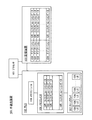
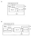
図1に、本発明の一態様に係る半導体装置100の構成を、ブロック図で例示する。なお、本明細書のブロック図では、回路を機能ごとに分類し、互いに独立したブロックとして示しているが、実際の回路は機能ごとに完全に切り分けることが難しく、一つの回路が複数の機能に係わることもあり得る。
本発明の一態様に係る半導体装置は、表示機器、パーソナルコンピュータ、記録媒体を備えた画像再生装置(代表的にはDVD:Digital Versatile Disc等の記録媒体を再生し、その画像を表示しうるディスプレイを有する装置)に用いることができる。その他に、本発明の一態様に係る半導体装置を用いることができる電子機器として、携帯電話、携帯型を含むゲーム機、携帯情報端末、電子書籍、ビデオカメラ、デジタルスチルカメラ、ゴーグル型ディスプレイ(ヘッドマウントディスプレイ)、ナビゲーションシステム、音響再生装置(カーオーディオ、デジタルオーディオプレイヤー等)、複写機、ファクシミリ、プリンター、プリンター複合機、現金自動預け入れ払い機(ATM)、自動販売機などが挙げられる。これら電子機器の具体例を図14に示す。
32 マルチプレクサ
33 マルチプレクサ
34 マルチプレクサ
35 マルチプレクサ
36 マルチプレクサ
37 マルチプレクサ
41 マルチプレクサ
42 マルチプレクサ
43 マルチプレクサ
44 OR回路
100 半導体装置
101 プロセッサ
102 PLD
103 記憶装置
104 アプリケーション
105 コンフィギュレーションデータ
106 LE
107 ロジックアレイ
108 メモリエレメント
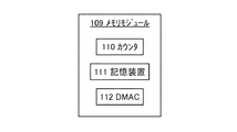
109 メモリモジュール
110 カウンタ
111 記憶装置
112 DMAC
120 メモリセル
120A スレッド
120B スレッド
120C スレッド
120D スレッド
121 記憶素子
122 スイッチ
122a トランジスタ
130 ゲート電極
131 ゲート絶縁膜
132 導電膜
133 導電膜
134 酸化物半導体膜
135 絶縁膜
150 メモリセル
151 トランジスタ
152 容量素子
153 メモリセル
154 トランジスタ
155 トランジスタ
156 容量素子
157 メモリセル
158 トランジスタ
159 トランジスタ
160 容量素子
161 駆動回路
162 入出力バッファ
163 メインアンプ
164 カラムデコーダ
165 ローデコーダ
166 スイッチ回路
167 プリチャージ回路
168 センスアンプ
169 回路
170 メモリセル
175 セルアレイ
180 LUT
181 レジスタ
182 コンフィギュレーションメモリ
310 ゲート電極
321 配線群
322 スイッチ
323 配線エレメント
324 出力端子
325 配線
326 配線
327 トランジスタ
328 トランジスタ
329 トランジスタ
330 トランジスタ
331 トランジスタ
332 トランジスタ
515 トランジスタ
516 トランジスタ
517 トランジスタ
518 トランジスタ
519 トランジスタ
520 トランジスタ
521 トランジスタ
522 トランジスタ
523 トランジスタ
601 制御装置
602 演算装置
603 メインメモリ
604 入力装置
605 出力装置
606 IF
607 緩衝記憶装置
5001 筐体
5002 筐体
5003 表示部
5004 表示部
5005 マイクロホン
5006 スピーカー
5007 操作キー
5008 スタイラス
5401 筐体
5402 表示部
5403 キーボード
5404 ポインティングデバイス
5601 筐体
5602 筐体
5603 表示部
5604 表示部
5605 接続部
5606 操作キー
5801 筐体
5802 筐体
5803 表示部
5804 操作キー
5805 レンズ
5806 接続部
Claims (7)
- 複数のアプリケーションプログラムと、前記複数のアプリケーションプログラムの各々に関連づけられた複数のコンフィギュレーションデータとが記憶された記憶装置と、
前記複数のアプリケーションプログラムの各々が有する第1スレッドを実行する機能を有するプロセッサと、
プログラマブルロジックデバイスと、を有し、
前記プログラマブルロジックデバイスは、メモリモジュールと、メモリエレメントと、複数のロジックエレメントと、を有し、
前記メモリエレメントは、前記複数のコンフィギュレーションデータのうち、前記メモリモジュールにより選択された複数のコンフィギュレーションデータを格納する機能を有し、
前記複数のロジックエレメントは、格納された前記複数のコンフィギュレーションデータに従って論理回路の定義を行う機能と、前記複数のアプリケーションプログラムの各々が有する第2スレッドを前記論理回路おいて実行する機能と、を有し、
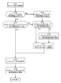
前記メモリモジュールは、前記複数のロジックエレメントにおいて前記論理回路の定義が行われるのに用いられた回数を、格納された前記複数のコンフィギュレーションデータごとにカウントする機能と、前記回数のデータを用いて、使用頻度が高いと見込まれるコンフィギュレーションデータの選択を行う機能と、を有し、
前記メモリエレメントは、記憶素子と、格納された前記複数のコンフィギュレーションデータによって定められた量の電荷を前記記憶素子に供給、保持、又は放出するためのスイッチとを、複数のメモリセルのそれぞれに有する半導体装置。 - 複数のアプリケーションプログラムと、前記複数のアプリケーションプログラムの各々に関連づけられた複数のコンフィギュレーションデータとが記憶された記憶装置と、
前記複数のアプリケーションプログラムの各々が有する第1スレッドを実行する機能を有するプロセッサと、
プログラマブルロジックデバイスと、を有し、
前記プログラマブルロジックデバイスは、メモリモジュールと、メモリエレメントと、複数のロジックエレメントと、を有し、
前記メモリエレメントは、前記複数のコンフィギュレーションデータのうち、前記メモリモジュールにより選択された複数のコンフィギュレーションデータを格納する機能を有し、
前記複数のロジックエレメントは、格納された前記複数のコンフィギュレーションデータに従って論理回路の定義を行う機能と、前記複数のアプリケーションプログラムの各々が有する第2スレッドを前記論理回路おいて実行する機能と、を有し、
前記メモリモジュールは、前記複数のロジックエレメントにおいて前記論理回路の定義が行われた時間のデータを取得する機能と、前記時間のデータを用いて、使用頻度が低いと見込まれるコンフィギュレーションデータの選択を行う機能と、を有し、
前記メモリエレメントは、記憶素子と、格納された前記複数のコンフィギュレーションデータによって定められた量の電荷を前記記憶素子に供給、保持、又は放出するためのスイッチとを、複数のメモリセルのそれぞれに有する半導体装置。 - 請求項2において、
前記時間のデータは、格納された前記複数のコンフィギュレーションデータの各々が、前記複数のロジックエレメントに書き込まれたときの時間を示すデータである半導体装置。 - 請求項2又は3において、
前記メモリモジュールは、前記使用頻度が低いと見込まれるコンフィギュレーションデータが格納されている記憶領域を特定し、別のコンフィギュレーションデータで上書きする機能を有する半導体装置。 - 請求項1乃至4のいずれか一において、
前記記憶素子は、トランジスタまたは容量素子である半導体装置。 - 請求項1乃至5のいずれか1項において、
前記スイッチは、チャネル形成領域に酸化物半導体を含むトランジスタを有する半導体装置。 - 請求項6において、
前記酸化物半導体は、In、Ga、及びZnを含む半導体装置。
Priority Applications (1)
| Application Number | Priority Date | Filing Date | Title |
|---|---|---|---|
| JP2013092167A JP6228381B2 (ja) | 2012-04-30 | 2013-04-25 | 半導体装置 |
Applications Claiming Priority (3)
| Application Number | Priority Date | Filing Date | Title |
|---|---|---|---|
| JP2012104282 | 2012-04-30 | ||
| JP2012104282 | 2012-04-30 | ||
| JP2013092167A JP6228381B2 (ja) | 2012-04-30 | 2013-04-25 | 半導体装置 |
Related Child Applications (1)
| Application Number | Title | Priority Date | Filing Date |
|---|---|---|---|
| JP2017199328A Division JP6554153B2 (ja) | 2012-04-30 | 2017-10-13 | 半導体装置の動作方法 |
Publications (3)
| Publication Number | Publication Date |
|---|---|
| JP2013251889A JP2013251889A (ja) | 2013-12-12 |
| JP2013251889A5 JP2013251889A5 (ja) | 2016-06-16 |
| JP6228381B2 true JP6228381B2 (ja) | 2017-11-08 |
Family
ID=49476706
Family Applications (3)
| Application Number | Title | Priority Date | Filing Date |
|---|---|---|---|
| JP2013092167A Expired - Fee Related JP6228381B2 (ja) | 2012-04-30 | 2013-04-25 | 半導体装置 |
| JP2017199328A Active JP6554153B2 (ja) | 2012-04-30 | 2017-10-13 | 半導体装置の動作方法 |
| JP2019001989A Expired - Fee Related JP6725709B2 (ja) | 2012-04-30 | 2019-01-09 | 半導体装置の動作方法 |
Family Applications After (2)
| Application Number | Title | Priority Date | Filing Date |
|---|---|---|---|
| JP2017199328A Active JP6554153B2 (ja) | 2012-04-30 | 2017-10-13 | 半導体装置の動作方法 |
| JP2019001989A Expired - Fee Related JP6725709B2 (ja) | 2012-04-30 | 2019-01-09 | 半導体装置の動作方法 |
Country Status (2)
| Country | Link |
|---|---|
| US (1) | US8896345B2 (ja) |
| JP (3) | JP6228381B2 (ja) |
Families Citing this family (12)
| Publication number | Priority date | Publication date | Assignee | Title |
|---|---|---|---|---|
| CN104321967B (zh) | 2012-05-25 | 2018-01-09 | 株式会社半导体能源研究所 | 可编程逻辑装置及半导体装置 |
| JP6377317B2 (ja) | 2012-05-30 | 2018-08-22 | 株式会社半導体エネルギー研究所 | プログラマブルロジックデバイス |
| JP6478562B2 (ja) | 2013-11-07 | 2019-03-06 | 株式会社半導体エネルギー研究所 | 半導体装置 |
| US9721968B2 (en) | 2014-02-06 | 2017-08-01 | Semiconductor Energy Laboratory Co., Ltd. | Semiconductor device, electronic component, and electronic appliance |
| CN105960633B (zh) * | 2014-02-07 | 2020-06-19 | 株式会社半导体能源研究所 | 半导体装置、装置及电子设备 |
| KR102267237B1 (ko) * | 2014-03-07 | 2021-06-18 | 가부시키가이샤 한도오따이 에네루기 켄큐쇼 | 반도체 장치 및 전자 기기 |
| JP6541376B2 (ja) | 2014-03-13 | 2019-07-10 | 株式会社半導体エネルギー研究所 | プログラマブルロジックデバイスの動作方法 |
| TWI643457B (zh) | 2014-04-25 | 2018-12-01 | 日商半導體能源研究所股份有限公司 | 半導體裝置 |
| KR102643895B1 (ko) | 2015-10-30 | 2024-03-05 | 가부시키가이샤 한도오따이 에네루기 켄큐쇼 | 반도체 장치, 전자 부품, 및 전자 기기 |
| JP2017135698A (ja) * | 2015-12-29 | 2017-08-03 | 株式会社半導体エネルギー研究所 | 半導体装置、コンピュータ及び電子機器 |
| CN107766090A (zh) * | 2016-08-15 | 2018-03-06 | 天津科畅慧通信息技术有限公司 | 一种基于epld协助cpu启动的方法及装置 |
| US11256520B2 (en) * | 2019-09-18 | 2022-02-22 | Xilinx, Inc. | Tracing status of a programmable device |
Family Cites Families (117)
| Publication number | Priority date | Publication date | Assignee | Title |
|---|---|---|---|---|
| JPS60198861A (ja) | 1984-03-23 | 1985-10-08 | Fujitsu Ltd | 薄膜トランジスタ |
| JPH0244256B2 (ja) | 1987-01-28 | 1990-10-03 | Kagaku Gijutsucho Mukizaishitsu Kenkyushocho | Ingazn2o5deshimesarerurotsuhoshokeinosojokozoojusurukagobutsuoyobisonoseizoho |
| JPH0244260B2 (ja) | 1987-02-24 | 1990-10-03 | Kagaku Gijutsucho Mukizaishitsu Kenkyushocho | Ingazn5o8deshimesarerurotsuhoshokeinosojokozoojusurukagobutsuoyobisonoseizoho |
| JPH0244258B2 (ja) | 1987-02-24 | 1990-10-03 | Kagaku Gijutsucho Mukizaishitsu Kenkyushocho | Ingazn3o6deshimesarerurotsuhoshokeinosojokozoojusurukagobutsuoyobisonoseizoho |
| JPS63210023A (ja) | 1987-02-24 | 1988-08-31 | Natl Inst For Res In Inorg Mater | InGaZn↓4O↓7で示される六方晶系の層状構造を有する化合物およびその製造法 |
| JPH0244262B2 (ja) | 1987-02-27 | 1990-10-03 | Kagaku Gijutsucho Mukizaishitsu Kenkyushocho | Ingazn6o9deshimesarerurotsuhoshokeinosojokozoojusurukagobutsuoyobisonoseizoho |
| JPH0244263B2 (ja) | 1987-04-22 | 1990-10-03 | Kagaku Gijutsucho Mukizaishitsu Kenkyushocho | Ingazn7o10deshimesarerurotsuhoshokeinosojokozoojusurukagobutsuoyobisonoseizoho |
| JPH02291720A (ja) * | 1989-05-01 | 1990-12-03 | Kawasaki Steel Corp | プログラム可能な論理デバイス |
| GB9108599D0 (en) * | 1991-04-22 | 1991-06-05 | Pilkington Micro Electronics | Peripheral controller |
| JPH05251705A (ja) | 1992-03-04 | 1993-09-28 | Fuji Xerox Co Ltd | 薄膜トランジスタ |
| JP3479375B2 (ja) | 1995-03-27 | 2003-12-15 | 科学技術振興事業団 | 亜酸化銅等の金属酸化物半導体による薄膜トランジスタとpn接合を形成した金属酸化物半導体装置およびそれらの製造方法 |
| US5646544A (en) * | 1995-06-05 | 1997-07-08 | International Business Machines Corporation | System and method for dynamically reconfiguring a programmable gate array |
| DE69635107D1 (de) | 1995-08-03 | 2005-09-29 | Koninkl Philips Electronics Nv | Halbleiteranordnung mit einem transparenten schaltungselement |
| JP3625598B2 (ja) | 1995-12-30 | 2005-03-02 | 三星電子株式会社 | 液晶表示装置の製造方法 |
| JP4170454B2 (ja) | 1998-07-24 | 2008-10-22 | Hoya株式会社 | 透明導電性酸化物薄膜を有する物品及びその製造方法 |
| JP2000150861A (ja) | 1998-11-16 | 2000-05-30 | Tdk Corp | 酸化物薄膜 |
| JP3276930B2 (ja) | 1998-11-17 | 2002-04-22 | 科学技術振興事業団 | トランジスタ及び半導体装置 |
| JP3684901B2 (ja) | 1999-03-02 | 2005-08-17 | 富士ゼロックス株式会社 | 情報処理システム |
| JP3743487B2 (ja) * | 1999-07-14 | 2006-02-08 | 富士ゼロックス株式会社 | プログラマブル論理回路装置、情報処理システム、プログラマブル論理回路装置への回路の再構成方法、プログラマブル論理回路装置用の回路情報の圧縮方法 |
| TW460731B (en) | 1999-09-03 | 2001-10-21 | Ind Tech Res Inst | Electrode structure and production method of wide viewing angle LCD |
| US6851047B1 (en) * | 1999-10-15 | 2005-02-01 | Xilinx, Inc. | Configuration in a configurable system on a chip |
| JP4089858B2 (ja) | 2000-09-01 | 2008-05-28 | 国立大学法人東北大学 | 半導体デバイス |
| KR20020038482A (ko) | 2000-11-15 | 2002-05-23 | 모리시타 요이찌 | 박막 트랜지스터 어레이, 그 제조방법 및 그것을 이용한표시패널 |
| JP3636986B2 (ja) * | 2000-12-06 | 2005-04-06 | 松下電器産業株式会社 | 半導体集積回路 |
| JP3997731B2 (ja) | 2001-03-19 | 2007-10-24 | 富士ゼロックス株式会社 | 基材上に結晶性半導体薄膜を形成する方法 |
| JP2002289859A (ja) | 2001-03-23 | 2002-10-04 | Minolta Co Ltd | 薄膜トランジスタ |
| JP4090716B2 (ja) | 2001-09-10 | 2008-05-28 | 雅司 川崎 | 薄膜トランジスタおよびマトリクス表示装置 |
| JP3925839B2 (ja) | 2001-09-10 | 2007-06-06 | シャープ株式会社 | 半導体記憶装置およびその試験方法 |
| JP4164562B2 (ja) | 2002-09-11 | 2008-10-15 | 独立行政法人科学技術振興機構 | ホモロガス薄膜を活性層として用いる透明薄膜電界効果型トランジスタ |
| WO2003040441A1 (fr) | 2001-11-05 | 2003-05-15 | Japan Science And Technology Agency | Film mince monocristallin homologue a super-reseau naturel, procede de preparation et dispositif dans lequel est utilise ledit film mince monocristallin |
| JP4083486B2 (ja) | 2002-02-21 | 2008-04-30 | 独立行政法人科学技術振興機構 | LnCuO(S,Se,Te)単結晶薄膜の製造方法 |
| US7049190B2 (en) | 2002-03-15 | 2006-05-23 | Sanyo Electric Co., Ltd. | Method for forming ZnO film, method for forming ZnO semiconductor layer, method for fabricating semiconductor device, and semiconductor device |
| JP3933591B2 (ja) | 2002-03-26 | 2007-06-20 | 淳二 城戸 | 有機エレクトロルミネッセント素子 |
| US7339187B2 (en) | 2002-05-21 | 2008-03-04 | State Of Oregon Acting By And Through The Oregon State Board Of Higher Education On Behalf Of Oregon State University | Transistor structures |
| JP3952856B2 (ja) * | 2002-05-28 | 2007-08-01 | コニカミノルタホールディングス株式会社 | キャッシュ方法 |
| JP4088763B2 (ja) * | 2002-06-13 | 2008-05-21 | コニカミノルタホールディングス株式会社 | コンピュータシステム及び該コンピュータシステムに適したハードウェア/ソフトウェアロジック並びにキャッシュ方法 |
| JP2004022625A (ja) | 2002-06-13 | 2004-01-22 | Murata Mfg Co Ltd | 半導体デバイス及び該半導体デバイスの製造方法 |
| US7105868B2 (en) | 2002-06-24 | 2006-09-12 | Cermet, Inc. | High-electron mobility transistor with zinc oxide |
| US7067843B2 (en) | 2002-10-11 | 2006-06-27 | E. I. Du Pont De Nemours And Company | Transparent oxide semiconductor thin film transistors |
| JP4166105B2 (ja) | 2003-03-06 | 2008-10-15 | シャープ株式会社 | 半導体装置およびその製造方法 |
| JP2004273732A (ja) | 2003-03-07 | 2004-09-30 | Sharp Corp | アクティブマトリクス基板およびその製造方法 |
| JP4108633B2 (ja) | 2003-06-20 | 2008-06-25 | シャープ株式会社 | 薄膜トランジスタおよびその製造方法ならびに電子デバイス |
| US7262463B2 (en) | 2003-07-25 | 2007-08-28 | Hewlett-Packard Development Company, L.P. | Transistor including a deposited channel region having a doped portion |
| JP4174402B2 (ja) * | 2003-09-26 | 2008-10-29 | 株式会社東芝 | 制御回路及びリコンフィギャラブル論理ブロック |
| US7282782B2 (en) | 2004-03-12 | 2007-10-16 | Hewlett-Packard Development Company, L.P. | Combined binary oxide semiconductor device |
| EP1737044B1 (en) | 2004-03-12 | 2014-12-10 | Japan Science and Technology Agency | Amorphous oxide and thin film transistor |
| US7297977B2 (en) | 2004-03-12 | 2007-11-20 | Hewlett-Packard Development Company, L.P. | Semiconductor device |
| US7145174B2 (en) | 2004-03-12 | 2006-12-05 | Hewlett-Packard Development Company, Lp. | Semiconductor device |
| US7211825B2 (en) | 2004-06-14 | 2007-05-01 | Yi-Chi Shih | Indium oxide-based thin film transistors and circuits |
| JP2006100760A (ja) | 2004-09-02 | 2006-04-13 | Casio Comput Co Ltd | 薄膜トランジスタおよびその製造方法 |
| US7285501B2 (en) | 2004-09-17 | 2007-10-23 | Hewlett-Packard Development Company, L.P. | Method of forming a solution processed device |
| JP3900499B2 (ja) * | 2004-10-27 | 2007-04-04 | インターナショナル・ビジネス・マシーンズ・コーポレーション | 再構成可能な、命令レベルのハードウェアによる高速化のためにマイクロプロセッサとともにfpgaテクノロジを使用する方法および装置 |
| US7298084B2 (en) | 2004-11-02 | 2007-11-20 | 3M Innovative Properties Company | Methods and displays utilizing integrated zinc oxide row and column drivers in conjunction with organic light emitting diodes |
| RU2358354C2 (ru) | 2004-11-10 | 2009-06-10 | Кэнон Кабусики Кайся | Светоизлучающее устройство |
| US7791072B2 (en) | 2004-11-10 | 2010-09-07 | Canon Kabushiki Kaisha | Display |
| US7863611B2 (en) | 2004-11-10 | 2011-01-04 | Canon Kabushiki Kaisha | Integrated circuits utilizing amorphous oxides |
| US7829444B2 (en) | 2004-11-10 | 2010-11-09 | Canon Kabushiki Kaisha | Field effect transistor manufacturing method |
| US7453065B2 (en) | 2004-11-10 | 2008-11-18 | Canon Kabushiki Kaisha | Sensor and image pickup device |
| WO2006051995A1 (en) | 2004-11-10 | 2006-05-18 | Canon Kabushiki Kaisha | Field effect transistor employing an amorphous oxide |
| CN102945857B (zh) | 2004-11-10 | 2015-06-03 | 佳能株式会社 | 无定形氧化物和场效应晶体管 |
| US7579224B2 (en) | 2005-01-21 | 2009-08-25 | Semiconductor Energy Laboratory Co., Ltd. | Method for manufacturing a thin film semiconductor device |
| TWI505473B (zh) | 2005-01-28 | 2015-10-21 | 半導體能源研究所股份有限公司 | 半導體裝置,電子裝置,和半導體裝置的製造方法 |
| TWI569441B (zh) | 2005-01-28 | 2017-02-01 | 半導體能源研究所股份有限公司 | 半導體裝置,電子裝置,和半導體裝置的製造方法 |
| US7858451B2 (en) | 2005-02-03 | 2010-12-28 | Semiconductor Energy Laboratory Co., Ltd. | Electronic device, semiconductor device and manufacturing method thereof |
| US7948171B2 (en) | 2005-02-18 | 2011-05-24 | Semiconductor Energy Laboratory Co., Ltd. | Light emitting device |
| US20060197092A1 (en) | 2005-03-03 | 2006-09-07 | Randy Hoffman | System and method for forming conductive material on a substrate |
| US8681077B2 (en) | 2005-03-18 | 2014-03-25 | Semiconductor Energy Laboratory Co., Ltd. | Semiconductor device, and display device, driving method and electronic apparatus thereof |
| US7544967B2 (en) | 2005-03-28 | 2009-06-09 | Massachusetts Institute Of Technology | Low voltage flexible organic/transparent transistor for selective gas sensing, photodetecting and CMOS device applications |
| US7645478B2 (en) | 2005-03-31 | 2010-01-12 | 3M Innovative Properties Company | Methods of making displays |
| US8300031B2 (en) | 2005-04-20 | 2012-10-30 | Semiconductor Energy Laboratory Co., Ltd. | Semiconductor device comprising transistor having gate and drain connected through a current-voltage conversion element |
| JP2006344849A (ja) | 2005-06-10 | 2006-12-21 | Casio Comput Co Ltd | 薄膜トランジスタ |
| US7691666B2 (en) | 2005-06-16 | 2010-04-06 | Eastman Kodak Company | Methods of making thin film transistors comprising zinc-oxide-based semiconductor materials and transistors made thereby |
| US7402506B2 (en) | 2005-06-16 | 2008-07-22 | Eastman Kodak Company | Methods of making thin film transistors comprising zinc-oxide-based semiconductor materials and transistors made thereby |
| US7507618B2 (en) | 2005-06-27 | 2009-03-24 | 3M Innovative Properties Company | Method for making electronic devices using metal oxide nanoparticles |
| KR100711890B1 (ko) | 2005-07-28 | 2007-04-25 | 삼성에스디아이 주식회사 | 유기 발광표시장치 및 그의 제조방법 |
| JP2007059128A (ja) | 2005-08-23 | 2007-03-08 | Canon Inc | 有機el表示装置およびその製造方法 |
| JP4280736B2 (ja) | 2005-09-06 | 2009-06-17 | キヤノン株式会社 | 半導体素子 |
| JP5116225B2 (ja) | 2005-09-06 | 2013-01-09 | キヤノン株式会社 | 酸化物半導体デバイスの製造方法 |
| JP4850457B2 (ja) | 2005-09-06 | 2012-01-11 | キヤノン株式会社 | 薄膜トランジスタ及び薄膜ダイオード |
| JP2007073705A (ja) | 2005-09-06 | 2007-03-22 | Canon Inc | 酸化物半導体チャネル薄膜トランジスタおよびその製造方法 |
| EP1995787A3 (en) | 2005-09-29 | 2012-01-18 | Semiconductor Energy Laboratory Co, Ltd. | Semiconductor device having oxide semiconductor layer and manufacturing method therof |
| JP5037808B2 (ja) | 2005-10-20 | 2012-10-03 | キヤノン株式会社 | アモルファス酸化物を用いた電界効果型トランジスタ、及び該トランジスタを用いた表示装置 |
| KR101050767B1 (ko) | 2005-11-15 | 2011-07-20 | 가부시키가이샤 한도오따이 에네루기 켄큐쇼 | 반도체장치 제조방법 |
| TWI292281B (en) | 2005-12-29 | 2008-01-01 | Ind Tech Res Inst | Pixel structure of active organic light emitting diode and method of fabricating the same |
| JP4978006B2 (ja) * | 2006-01-05 | 2012-07-18 | 日本電気株式会社 | データ処理装置及びデータ処理方法 |
| US7867636B2 (en) | 2006-01-11 | 2011-01-11 | Murata Manufacturing Co., Ltd. | Transparent conductive film and method for manufacturing the same |
| JP4977478B2 (ja) | 2006-01-21 | 2012-07-18 | 三星電子株式会社 | ZnOフィルム及びこれを用いたTFTの製造方法 |
| US7576394B2 (en) | 2006-02-02 | 2009-08-18 | Kochi Industrial Promotion Center | Thin film transistor including low resistance conductive thin films and manufacturing method thereof |
| JP2007207136A (ja) * | 2006-02-06 | 2007-08-16 | Nec Corp | データ処理装置、データ処理方法、及びデータ処理プログラム |
| US7977169B2 (en) | 2006-02-15 | 2011-07-12 | Kochi Industrial Promotion Center | Semiconductor device including active layer made of zinc oxide with controlled orientations and manufacturing method thereof |
| KR20070101595A (ko) | 2006-04-11 | 2007-10-17 | 삼성전자주식회사 | ZnO TFT |
| US20070252928A1 (en) | 2006-04-28 | 2007-11-01 | Toppan Printing Co., Ltd. | Structure, transmission type liquid crystal display, reflection type display and manufacturing method thereof |
| JP5028033B2 (ja) | 2006-06-13 | 2012-09-19 | キヤノン株式会社 | 酸化物半導体膜のドライエッチング方法 |
| JP4609797B2 (ja) | 2006-08-09 | 2011-01-12 | Nec液晶テクノロジー株式会社 | 薄膜デバイス及びその製造方法 |
| JP4999400B2 (ja) | 2006-08-09 | 2012-08-15 | キヤノン株式会社 | 酸化物半導体膜のドライエッチング方法 |
| JP4853185B2 (ja) * | 2006-08-29 | 2012-01-11 | 富士ゼロックス株式会社 | 情報処理システム |
| JP4332545B2 (ja) | 2006-09-15 | 2009-09-16 | キヤノン株式会社 | 電界効果型トランジスタ及びその製造方法 |
| JP5164357B2 (ja) | 2006-09-27 | 2013-03-21 | キヤノン株式会社 | 半導体装置及び半導体装置の製造方法 |
| JP4274219B2 (ja) | 2006-09-27 | 2009-06-03 | セイコーエプソン株式会社 | 電子デバイス、有機エレクトロルミネッセンス装置、有機薄膜半導体装置 |
| US7622371B2 (en) | 2006-10-10 | 2009-11-24 | Hewlett-Packard Development Company, L.P. | Fused nanocrystal thin film semiconductor and method |
| US7772021B2 (en) | 2006-11-29 | 2010-08-10 | Samsung Electronics Co., Ltd. | Flat panel displays comprising a thin-film transistor having a semiconductive oxide in its channel and methods of fabricating the same for use in flat panel displays |
| JP2008140684A (ja) | 2006-12-04 | 2008-06-19 | Toppan Printing Co Ltd | カラーelディスプレイおよびその製造方法 |
| KR101303578B1 (ko) | 2007-01-05 | 2013-09-09 | 삼성전자주식회사 | 박막 식각 방법 |
| US8207063B2 (en) | 2007-01-26 | 2012-06-26 | Eastman Kodak Company | Process for atomic layer deposition |
| JP4659774B2 (ja) * | 2007-03-07 | 2011-03-30 | 三菱電機株式会社 | 電気機器 |
| KR100851215B1 (ko) | 2007-03-14 | 2008-08-07 | 삼성에스디아이 주식회사 | 박막 트랜지스터 및 이를 이용한 유기 전계 발광표시장치 |
| US7795613B2 (en) | 2007-04-17 | 2010-09-14 | Toppan Printing Co., Ltd. | Structure with transistor |
| KR101325053B1 (ko) | 2007-04-18 | 2013-11-05 | 삼성디스플레이 주식회사 | 박막 트랜지스터 기판 및 이의 제조 방법 |
| KR20080094300A (ko) | 2007-04-19 | 2008-10-23 | 삼성전자주식회사 | 박막 트랜지스터 및 그 제조 방법과 박막 트랜지스터를포함하는 평판 디스플레이 |
| KR101334181B1 (ko) | 2007-04-20 | 2013-11-28 | 삼성전자주식회사 | 선택적으로 결정화된 채널층을 갖는 박막 트랜지스터 및 그제조 방법 |
| US8274078B2 (en) | 2007-04-25 | 2012-09-25 | Canon Kabushiki Kaisha | Metal oxynitride semiconductor containing zinc |
| KR101345376B1 (ko) | 2007-05-29 | 2013-12-24 | 삼성전자주식회사 | ZnO 계 박막 트랜지스터 및 그 제조방법 |
| JP5215158B2 (ja) | 2007-12-17 | 2013-06-19 | 富士フイルム株式会社 | 無機結晶性配向膜及びその製造方法、半導体デバイス |
| JP4623179B2 (ja) | 2008-09-18 | 2011-02-02 | ソニー株式会社 | 薄膜トランジスタおよびその製造方法 |
| JP5451280B2 (ja) | 2008-10-09 | 2014-03-26 | キヤノン株式会社 | ウルツ鉱型結晶成長用基板およびその製造方法ならびに半導体装置 |
| KR101978106B1 (ko) * | 2010-01-20 | 2019-05-13 | 가부시키가이샤 한도오따이 에네루기 켄큐쇼 | 반도체 장치 |
| KR101899880B1 (ko) | 2011-02-17 | 2018-09-18 | 가부시키가이샤 한도오따이 에네루기 켄큐쇼 | 프로그래머블 lsi |
-
2013
- 2013-04-25 JP JP2013092167A patent/JP6228381B2/ja not_active Expired - Fee Related
- 2013-04-29 US US13/872,469 patent/US8896345B2/en not_active Expired - Fee Related
-
2017
- 2017-10-13 JP JP2017199328A patent/JP6554153B2/ja active Active
-
2019
- 2019-01-09 JP JP2019001989A patent/JP6725709B2/ja not_active Expired - Fee Related
Also Published As
| Publication number | Publication date |
|---|---|
| JP6554153B2 (ja) | 2019-07-31 |
| JP2018038052A (ja) | 2018-03-08 |
| US20130285698A1 (en) | 2013-10-31 |
| JP2019088012A (ja) | 2019-06-06 |
| US8896345B2 (en) | 2014-11-25 |
| JP2013251889A (ja) | 2013-12-12 |
| JP6725709B2 (ja) | 2020-07-22 |
Similar Documents
| Publication | Publication Date | Title |
|---|---|---|
| JP6725709B2 (ja) | 半導体装置の動作方法 | |
| JP6908663B2 (ja) | 記憶装置 | |
| JP6815446B2 (ja) | 半導体装置 | |
| JP6697023B2 (ja) | 半導体装置 | |
| US9165632B2 (en) | Memory device and semiconductor device | |
| US10090023B2 (en) | Memory device including memory circuit and selection circuit | |
| US9154136B2 (en) | Programmable logic device and semiconductor device | |
| JP6611851B2 (ja) | 記憶装置及び半導体装置 | |
| JP2020010354A (ja) | 半導体装置 | |
| US9257173B2 (en) | Arithmetic processing unit and driving method thereof | |
| JP6333589B2 (ja) | 半導体装置 | |
| US8873308B2 (en) | Signal processing circuit | |
| JP2021101556A (ja) | 半導体装置及び電子機器 |
Legal Events
| Date | Code | Title | Description |
|---|---|---|---|
| A521 | Request for written amendment filed |
Free format text: JAPANESE INTERMEDIATE CODE: A523 Effective date: 20160422 |
|
| A621 | Written request for application examination |
Free format text: JAPANESE INTERMEDIATE CODE: A621 Effective date: 20160422 |
|
| A977 | Report on retrieval |
Free format text: JAPANESE INTERMEDIATE CODE: A971007 Effective date: 20161206 |
|
| A131 | Notification of reasons for refusal |
Free format text: JAPANESE INTERMEDIATE CODE: A131 Effective date: 20161213 |
|
| A601 | Written request for extension of time |
Free format text: JAPANESE INTERMEDIATE CODE: A601 Effective date: 20170207 |
|
| A521 | Request for written amendment filed |
Free format text: JAPANESE INTERMEDIATE CODE: A523 Effective date: 20170407 |
|
| TRDD | Decision of grant or rejection written | ||
| A01 | Written decision to grant a patent or to grant a registration (utility model) |
Free format text: JAPANESE INTERMEDIATE CODE: A01 Effective date: 20170919 |
|
| A61 | First payment of annual fees (during grant procedure) |
Free format text: JAPANESE INTERMEDIATE CODE: A61 Effective date: 20171013 |
|
| R150 | Certificate of patent or registration of utility model |
Ref document number: 6228381 Country of ref document: JP Free format text: JAPANESE INTERMEDIATE CODE: R150 |
|
| R250 | Receipt of annual fees |
Free format text: JAPANESE INTERMEDIATE CODE: R250 |
|
| LAPS | Cancellation because of no payment of annual fees |