JP6157998B2 - 半導体装置 - Google Patents
半導体装置 Download PDFInfo
- Publication number
- JP6157998B2 JP6157998B2 JP2013182363A JP2013182363A JP6157998B2 JP 6157998 B2 JP6157998 B2 JP 6157998B2 JP 2013182363 A JP2013182363 A JP 2013182363A JP 2013182363 A JP2013182363 A JP 2013182363A JP 6157998 B2 JP6157998 B2 JP 6157998B2
- Authority
- JP
- Japan
- Prior art keywords
- wiring board
- view
- plan
- semiconductor device
- corner
- Prior art date
- Legal status (The legal status is an assumption and is not a legal conclusion. Google has not performed a legal analysis and makes no representation as to the accuracy of the status listed.)
- Active
Links
- 239000004065 semiconductor Substances 0.000 title claims description 174
- 239000000758 substrate Substances 0.000 claims description 22
- 229910000679 solder Inorganic materials 0.000 claims description 8
- 239000004020 conductor Substances 0.000 claims description 6
- 229910052751 metal Inorganic materials 0.000 claims description 4
- 239000002184 metal Substances 0.000 claims description 4
- 230000002093 peripheral effect Effects 0.000 claims 20
- 239000000853 adhesive Substances 0.000 claims 2
- 230000001070 adhesive effect Effects 0.000 claims 2
- 239000000463 material Substances 0.000 claims 2
- 101100260207 Schizosaccharomyces pombe (strain 972 / ATCC 24843) sfc2 gene Proteins 0.000 description 49
- 230000004048 modification Effects 0.000 description 35
- 238000012986 modification Methods 0.000 description 35
- 101150031442 sfc1 gene Proteins 0.000 description 33
- 101001050240 Arabidopsis thaliana Adenylate kinase 2, chloroplastic Proteins 0.000 description 26
- 239000011347 resin Substances 0.000 description 22
- 229920005989 resin Polymers 0.000 description 22
- 102100039246 Elongator complex protein 1 Human genes 0.000 description 13
- 101710167754 Elongator complex protein 1 Proteins 0.000 description 13
- 238000007789 sealing Methods 0.000 description 13
- 238000000034 method Methods 0.000 description 11
- 238000004519 manufacturing process Methods 0.000 description 10
- 238000010586 diagram Methods 0.000 description 9
- 239000010410 layer Substances 0.000 description 8
- 101001057036 Arabidopsis thaliana Adenylate kinase 1, chloroplastic Proteins 0.000 description 6
- 101100365570 Schizosaccharomyces pombe (strain 972 / ATCC 24843) sfc3 gene Proteins 0.000 description 6
- 101100365571 Schizosaccharomyces pombe (strain 972 / ATCC 24843) sfc4 gene Proteins 0.000 description 6
- 239000012790 adhesive layer Substances 0.000 description 6
- 230000000694 effects Effects 0.000 description 5
- 230000015572 biosynthetic process Effects 0.000 description 4
- 238000002955 isolation Methods 0.000 description 4
- 229910021420 polycrystalline silicon Inorganic materials 0.000 description 4
- 229920005591 polysilicon Polymers 0.000 description 4
- 101100256921 Ajellomyces capsulatus SID3 gene Proteins 0.000 description 3
- 101100064323 Arabidopsis thaliana DTX47 gene Proteins 0.000 description 3
- 101000840469 Arabidopsis thaliana Isochorismate synthase 1, chloroplastic Proteins 0.000 description 3
- 102100034241 Elongator complex protein 2 Human genes 0.000 description 3
- 101710167764 Elongator complex protein 2 Proteins 0.000 description 3
- 101150026676 SID1 gene Proteins 0.000 description 3
- 101100366400 Schizosaccharomyces pombe (strain 972 / ATCC 24843) spg1 gene Proteins 0.000 description 3
- VYPSYNLAJGMNEJ-UHFFFAOYSA-N Silicium dioxide Chemical compound O=[Si]=O VYPSYNLAJGMNEJ-UHFFFAOYSA-N 0.000 description 3
- 101150096768 sid4 gene Proteins 0.000 description 3
- 229910052814 silicon oxide Inorganic materials 0.000 description 3
- 101001021281 Homo sapiens Protein HEXIM1 Proteins 0.000 description 2
- 101000693265 Homo sapiens Sphingosine 1-phosphate receptor 1 Proteins 0.000 description 2
- 101000693269 Homo sapiens Sphingosine 1-phosphate receptor 3 Proteins 0.000 description 2
- 102100025750 Sphingosine 1-phosphate receptor 1 Human genes 0.000 description 2
- 102100025747 Sphingosine 1-phosphate receptor 3 Human genes 0.000 description 2
- 239000003990 capacitor Substances 0.000 description 2
- 230000004907 flux Effects 0.000 description 2
- 230000001681 protective effect Effects 0.000 description 2
- BPQQTUXANYXVAA-UHFFFAOYSA-N Orthosilicate Chemical compound [O-][Si]([O-])([O-])[O-] BPQQTUXANYXVAA-UHFFFAOYSA-N 0.000 description 1
- XUIMIQQOPSSXEZ-UHFFFAOYSA-N Silicon Chemical compound [Si] XUIMIQQOPSSXEZ-UHFFFAOYSA-N 0.000 description 1
- ATJFFYVFTNAWJD-UHFFFAOYSA-N Tin Chemical compound [Sn] ATJFFYVFTNAWJD-UHFFFAOYSA-N 0.000 description 1
- 238000005520 cutting process Methods 0.000 description 1
- 230000014509 gene expression Effects 0.000 description 1
- 229910052735 hafnium Inorganic materials 0.000 description 1
- VBJZVLUMGGDVMO-UHFFFAOYSA-N hafnium atom Chemical compound [Hf] VBJZVLUMGGDVMO-UHFFFAOYSA-N 0.000 description 1
- 239000012535 impurity Substances 0.000 description 1
- 238000002161 passivation Methods 0.000 description 1
- 238000007650 screen-printing Methods 0.000 description 1
- 229910052710 silicon Inorganic materials 0.000 description 1
- 239000010703 silicon Substances 0.000 description 1
- 238000005728 strengthening Methods 0.000 description 1
Images


Classifications
-
- H—ELECTRICITY
- H01—ELECTRIC ELEMENTS
- H01L—SEMICONDUCTOR DEVICES NOT COVERED BY CLASS H10
- H01L23/00—Details of semiconductor or other solid state devices
- H01L23/02—Containers; Seals
- H01L23/04—Containers; Seals characterised by the shape of the container or parts, e.g. caps, walls
-
- H—ELECTRICITY
- H01—ELECTRIC ELEMENTS
- H01L—SEMICONDUCTOR DEVICES NOT COVERED BY CLASS H10
- H01L21/00—Processes or apparatus adapted for the manufacture or treatment of semiconductor or solid state devices or of parts thereof
- H01L21/02—Manufacture or treatment of semiconductor devices or of parts thereof
- H01L21/04—Manufacture or treatment of semiconductor devices or of parts thereof the devices having potential barriers, e.g. a PN junction, depletion layer or carrier concentration layer
- H01L21/50—Assembly of semiconductor devices using processes or apparatus not provided for in a single one of the subgroups H01L21/06 - H01L21/326, e.g. sealing of a cap to a base of a container
-
- H—ELECTRICITY
- H01—ELECTRIC ELEMENTS
- H01L—SEMICONDUCTOR DEVICES NOT COVERED BY CLASS H10
- H01L23/00—Details of semiconductor or other solid state devices
- H01L23/34—Arrangements for cooling, heating, ventilating or temperature compensation ; Temperature sensing arrangements
- H01L23/36—Selection of materials, or shaping, to facilitate cooling or heating, e.g. heatsinks
- H01L23/367—Cooling facilitated by shape of device
- H01L23/3675—Cooling facilitated by shape of device characterised by the shape of the housing
-
- H—ELECTRICITY
- H01—ELECTRIC ELEMENTS
- H01L—SEMICONDUCTOR DEVICES NOT COVERED BY CLASS H10
- H01L23/00—Details of semiconductor or other solid state devices
- H01L23/34—Arrangements for cooling, heating, ventilating or temperature compensation ; Temperature sensing arrangements
- H01L23/36—Selection of materials, or shaping, to facilitate cooling or heating, e.g. heatsinks
- H01L23/373—Cooling facilitated by selection of materials for the device or materials for thermal expansion adaptation, e.g. carbon
- H01L23/3736—Metallic materials
-
- H—ELECTRICITY
- H01—ELECTRIC ELEMENTS
- H01L—SEMICONDUCTOR DEVICES NOT COVERED BY CLASS H10
- H01L23/00—Details of semiconductor or other solid state devices
- H01L23/48—Arrangements for conducting electric current to or from the solid state body in operation, e.g. leads, terminal arrangements ; Selection of materials therefor
- H01L23/488—Arrangements for conducting electric current to or from the solid state body in operation, e.g. leads, terminal arrangements ; Selection of materials therefor consisting of soldered or bonded constructions
- H01L23/498—Leads, i.e. metallisations or lead-frames on insulating substrates, e.g. chip carriers
- H01L23/49838—Geometry or layout
-
- H—ELECTRICITY
- H01—ELECTRIC ELEMENTS
- H01L—SEMICONDUCTOR DEVICES NOT COVERED BY CLASS H10
- H01L23/00—Details of semiconductor or other solid state devices
- H01L23/544—Marks applied to semiconductor devices or parts, e.g. registration marks, alignment structures, wafer maps
-
- H—ELECTRICITY
- H01—ELECTRIC ELEMENTS
- H01L—SEMICONDUCTOR DEVICES NOT COVERED BY CLASS H10
- H01L24/00—Arrangements for connecting or disconnecting semiconductor or solid-state bodies; Methods or apparatus related thereto
- H01L24/01—Means for bonding being attached to, or being formed on, the surface to be connected, e.g. chip-to-package, die-attach, "first-level" interconnects; Manufacturing methods related thereto
- H01L24/02—Bonding areas ; Manufacturing methods related thereto
- H01L24/07—Structure, shape, material or disposition of the bonding areas after the connecting process
- H01L24/09—Structure, shape, material or disposition of the bonding areas after the connecting process of a plurality of bonding areas
-
- H—ELECTRICITY
- H01—ELECTRIC ELEMENTS
- H01L—SEMICONDUCTOR DEVICES NOT COVERED BY CLASS H10
- H01L24/00—Arrangements for connecting or disconnecting semiconductor or solid-state bodies; Methods or apparatus related thereto
- H01L24/74—Apparatus for manufacturing arrangements for connecting or disconnecting semiconductor or solid-state bodies
-
- H—ELECTRICITY
- H01—ELECTRIC ELEMENTS
- H01L—SEMICONDUCTOR DEVICES NOT COVERED BY CLASS H10
- H01L24/00—Arrangements for connecting or disconnecting semiconductor or solid-state bodies; Methods or apparatus related thereto
- H01L24/93—Batch processes
- H01L24/95—Batch processes at chip-level, i.e. with connecting carried out on a plurality of singulated devices, i.e. on diced chips
- H01L24/97—Batch processes at chip-level, i.e. with connecting carried out on a plurality of singulated devices, i.e. on diced chips the devices being connected to a common substrate, e.g. interposer, said common substrate being separable into individual assemblies after connecting
-
- H—ELECTRICITY
- H01—ELECTRIC ELEMENTS
- H01L—SEMICONDUCTOR DEVICES NOT COVERED BY CLASS H10
- H01L25/00—Assemblies consisting of a plurality of individual semiconductor or other solid state devices ; Multistep manufacturing processes thereof
- H01L25/16—Assemblies consisting of a plurality of individual semiconductor or other solid state devices ; Multistep manufacturing processes thereof the devices being of types provided for in two or more different main groups of groups H01L27/00 - H01L33/00, or in a single subclass of H10K, H10N, e.g. forming hybrid circuits
- H01L25/165—Containers
-
- H—ELECTRICITY
- H05—ELECTRIC TECHNIQUES NOT OTHERWISE PROVIDED FOR
- H05K—PRINTED CIRCUITS; CASINGS OR CONSTRUCTIONAL DETAILS OF ELECTRIC APPARATUS; MANUFACTURE OF ASSEMBLAGES OF ELECTRICAL COMPONENTS
- H05K1/00—Printed circuits
- H05K1/02—Details
- H05K1/0266—Marks, test patterns or identification means
-
- H—ELECTRICITY
- H01—ELECTRIC ELEMENTS
- H01L—SEMICONDUCTOR DEVICES NOT COVERED BY CLASS H10
- H01L2223/00—Details relating to semiconductor or other solid state devices covered by the group H01L23/00
- H01L2223/544—Marks applied to semiconductor devices or parts
- H01L2223/5442—Marks applied to semiconductor devices or parts comprising non digital, non alphanumeric information, e.g. symbols
-
- H—ELECTRICITY
- H01—ELECTRIC ELEMENTS
- H01L—SEMICONDUCTOR DEVICES NOT COVERED BY CLASS H10
- H01L2223/00—Details relating to semiconductor or other solid state devices covered by the group H01L23/00
- H01L2223/544—Marks applied to semiconductor devices or parts
- H01L2223/54426—Marks applied to semiconductor devices or parts for alignment
-
- H—ELECTRICITY
- H01—ELECTRIC ELEMENTS
- H01L—SEMICONDUCTOR DEVICES NOT COVERED BY CLASS H10
- H01L2223/00—Details relating to semiconductor or other solid state devices covered by the group H01L23/00
- H01L2223/544—Marks applied to semiconductor devices or parts
- H01L2223/54473—Marks applied to semiconductor devices or parts for use after dicing
- H01L2223/54486—Located on package parts, e.g. encapsulation, leads, package substrate
-
- H—ELECTRICITY
- H01—ELECTRIC ELEMENTS
- H01L—SEMICONDUCTOR DEVICES NOT COVERED BY CLASS H10
- H01L2224/00—Indexing scheme for arrangements for connecting or disconnecting semiconductor or solid-state bodies and methods related thereto as covered by H01L24/00
- H01L2224/01—Means for bonding being attached to, or being formed on, the surface to be connected, e.g. chip-to-package, die-attach, "first-level" interconnects; Manufacturing methods related thereto
- H01L2224/02—Bonding areas; Manufacturing methods related thereto
- H01L2224/04—Structure, shape, material or disposition of the bonding areas prior to the connecting process
- H01L2224/0401—Bonding areas specifically adapted for bump connectors, e.g. under bump metallisation [UBM]
-
- H—ELECTRICITY
- H01—ELECTRIC ELEMENTS
- H01L—SEMICONDUCTOR DEVICES NOT COVERED BY CLASS H10
- H01L2224/00—Indexing scheme for arrangements for connecting or disconnecting semiconductor or solid-state bodies and methods related thereto as covered by H01L24/00
- H01L2224/01—Means for bonding being attached to, or being formed on, the surface to be connected, e.g. chip-to-package, die-attach, "first-level" interconnects; Manufacturing methods related thereto
- H01L2224/02—Bonding areas; Manufacturing methods related thereto
- H01L2224/04—Structure, shape, material or disposition of the bonding areas prior to the connecting process
- H01L2224/04042—Bonding areas specifically adapted for wire connectors, e.g. wirebond pads
-
- H—ELECTRICITY
- H01—ELECTRIC ELEMENTS
- H01L—SEMICONDUCTOR DEVICES NOT COVERED BY CLASS H10
- H01L2224/00—Indexing scheme for arrangements for connecting or disconnecting semiconductor or solid-state bodies and methods related thereto as covered by H01L24/00
- H01L2224/01—Means for bonding being attached to, or being formed on, the surface to be connected, e.g. chip-to-package, die-attach, "first-level" interconnects; Manufacturing methods related thereto
- H01L2224/02—Bonding areas; Manufacturing methods related thereto
- H01L2224/07—Structure, shape, material or disposition of the bonding areas after the connecting process
- H01L2224/09—Structure, shape, material or disposition of the bonding areas after the connecting process of a plurality of bonding areas
- H01L2224/091—Disposition
- H01L2224/0912—Layout
- H01L2224/0913—Square or rectangular array
-
- H—ELECTRICITY
- H01—ELECTRIC ELEMENTS
- H01L—SEMICONDUCTOR DEVICES NOT COVERED BY CLASS H10
- H01L2224/00—Indexing scheme for arrangements for connecting or disconnecting semiconductor or solid-state bodies and methods related thereto as covered by H01L24/00
- H01L2224/01—Means for bonding being attached to, or being formed on, the surface to be connected, e.g. chip-to-package, die-attach, "first-level" interconnects; Manufacturing methods related thereto
- H01L2224/10—Bump connectors; Manufacturing methods related thereto
- H01L2224/12—Structure, shape, material or disposition of the bump connectors prior to the connecting process
- H01L2224/13—Structure, shape, material or disposition of the bump connectors prior to the connecting process of an individual bump connector
- H01L2224/13001—Core members of the bump connector
- H01L2224/13099—Material
- H01L2224/131—Material with a principal constituent of the material being a metal or a metalloid, e.g. boron [B], silicon [Si], germanium [Ge], arsenic [As], antimony [Sb], tellurium [Te] and polonium [Po], and alloys thereof
- H01L2224/13101—Material with a principal constituent of the material being a metal or a metalloid, e.g. boron [B], silicon [Si], germanium [Ge], arsenic [As], antimony [Sb], tellurium [Te] and polonium [Po], and alloys thereof the principal constituent melting at a temperature of less than 400°C
-
- H—ELECTRICITY
- H01—ELECTRIC ELEMENTS
- H01L—SEMICONDUCTOR DEVICES NOT COVERED BY CLASS H10
- H01L2224/00—Indexing scheme for arrangements for connecting or disconnecting semiconductor or solid-state bodies and methods related thereto as covered by H01L24/00
- H01L2224/01—Means for bonding being attached to, or being formed on, the surface to be connected, e.g. chip-to-package, die-attach, "first-level" interconnects; Manufacturing methods related thereto
- H01L2224/10—Bump connectors; Manufacturing methods related thereto
- H01L2224/12—Structure, shape, material or disposition of the bump connectors prior to the connecting process
- H01L2224/13—Structure, shape, material or disposition of the bump connectors prior to the connecting process of an individual bump connector
- H01L2224/13001—Core members of the bump connector
- H01L2224/13099—Material
- H01L2224/131—Material with a principal constituent of the material being a metal or a metalloid, e.g. boron [B], silicon [Si], germanium [Ge], arsenic [As], antimony [Sb], tellurium [Te] and polonium [Po], and alloys thereof
- H01L2224/13138—Material with a principal constituent of the material being a metal or a metalloid, e.g. boron [B], silicon [Si], germanium [Ge], arsenic [As], antimony [Sb], tellurium [Te] and polonium [Po], and alloys thereof the principal constituent melting at a temperature of greater than or equal to 950°C and less than 1550°C
- H01L2224/13144—Gold [Au] as principal constituent
-
- H—ELECTRICITY
- H01—ELECTRIC ELEMENTS
- H01L—SEMICONDUCTOR DEVICES NOT COVERED BY CLASS H10
- H01L2224/00—Indexing scheme for arrangements for connecting or disconnecting semiconductor or solid-state bodies and methods related thereto as covered by H01L24/00
- H01L2224/01—Means for bonding being attached to, or being formed on, the surface to be connected, e.g. chip-to-package, die-attach, "first-level" interconnects; Manufacturing methods related thereto
- H01L2224/10—Bump connectors; Manufacturing methods related thereto
- H01L2224/12—Structure, shape, material or disposition of the bump connectors prior to the connecting process
- H01L2224/13—Structure, shape, material or disposition of the bump connectors prior to the connecting process of an individual bump connector
- H01L2224/13001—Core members of the bump connector
- H01L2224/13099—Material
- H01L2224/131—Material with a principal constituent of the material being a metal or a metalloid, e.g. boron [B], silicon [Si], germanium [Ge], arsenic [As], antimony [Sb], tellurium [Te] and polonium [Po], and alloys thereof
- H01L2224/13138—Material with a principal constituent of the material being a metal or a metalloid, e.g. boron [B], silicon [Si], germanium [Ge], arsenic [As], antimony [Sb], tellurium [Te] and polonium [Po], and alloys thereof the principal constituent melting at a temperature of greater than or equal to 950°C and less than 1550°C
- H01L2224/13147—Copper [Cu] as principal constituent
-
- H—ELECTRICITY
- H01—ELECTRIC ELEMENTS
- H01L—SEMICONDUCTOR DEVICES NOT COVERED BY CLASS H10
- H01L2224/00—Indexing scheme for arrangements for connecting or disconnecting semiconductor or solid-state bodies and methods related thereto as covered by H01L24/00
- H01L2224/01—Means for bonding being attached to, or being formed on, the surface to be connected, e.g. chip-to-package, die-attach, "first-level" interconnects; Manufacturing methods related thereto
- H01L2224/10—Bump connectors; Manufacturing methods related thereto
- H01L2224/15—Structure, shape, material or disposition of the bump connectors after the connecting process
- H01L2224/16—Structure, shape, material or disposition of the bump connectors after the connecting process of an individual bump connector
- H01L2224/161—Disposition
- H01L2224/16151—Disposition the bump connector connecting between a semiconductor or solid-state body and an item not being a semiconductor or solid-state body, e.g. chip-to-substrate, chip-to-passive
- H01L2224/16221—Disposition the bump connector connecting between a semiconductor or solid-state body and an item not being a semiconductor or solid-state body, e.g. chip-to-substrate, chip-to-passive the body and the item being stacked
- H01L2224/16225—Disposition the bump connector connecting between a semiconductor or solid-state body and an item not being a semiconductor or solid-state body, e.g. chip-to-substrate, chip-to-passive the body and the item being stacked the item being non-metallic, e.g. insulating substrate with or without metallisation
-
- H—ELECTRICITY
- H01—ELECTRIC ELEMENTS
- H01L—SEMICONDUCTOR DEVICES NOT COVERED BY CLASS H10
- H01L2224/00—Indexing scheme for arrangements for connecting or disconnecting semiconductor or solid-state bodies and methods related thereto as covered by H01L24/00
- H01L2224/01—Means for bonding being attached to, or being formed on, the surface to be connected, e.g. chip-to-package, die-attach, "first-level" interconnects; Manufacturing methods related thereto
- H01L2224/26—Layer connectors, e.g. plate connectors, solder or adhesive layers; Manufacturing methods related thereto
- H01L2224/31—Structure, shape, material or disposition of the layer connectors after the connecting process
- H01L2224/32—Structure, shape, material or disposition of the layer connectors after the connecting process of an individual layer connector
- H01L2224/321—Disposition
- H01L2224/32151—Disposition the layer connector connecting between a semiconductor or solid-state body and an item not being a semiconductor or solid-state body, e.g. chip-to-substrate, chip-to-passive
- H01L2224/32221—Disposition the layer connector connecting between a semiconductor or solid-state body and an item not being a semiconductor or solid-state body, e.g. chip-to-substrate, chip-to-passive the body and the item being stacked
- H01L2224/32225—Disposition the layer connector connecting between a semiconductor or solid-state body and an item not being a semiconductor or solid-state body, e.g. chip-to-substrate, chip-to-passive the body and the item being stacked the item being non-metallic, e.g. insulating substrate with or without metallisation
-
- H—ELECTRICITY
- H01—ELECTRIC ELEMENTS
- H01L—SEMICONDUCTOR DEVICES NOT COVERED BY CLASS H10
- H01L2224/00—Indexing scheme for arrangements for connecting or disconnecting semiconductor or solid-state bodies and methods related thereto as covered by H01L24/00
- H01L2224/01—Means for bonding being attached to, or being formed on, the surface to be connected, e.g. chip-to-package, die-attach, "first-level" interconnects; Manufacturing methods related thereto
- H01L2224/42—Wire connectors; Manufacturing methods related thereto
- H01L2224/47—Structure, shape, material or disposition of the wire connectors after the connecting process
- H01L2224/48—Structure, shape, material or disposition of the wire connectors after the connecting process of an individual wire connector
- H01L2224/4805—Shape
- H01L2224/4809—Loop shape
- H01L2224/48091—Arched
-
- H—ELECTRICITY
- H01—ELECTRIC ELEMENTS
- H01L—SEMICONDUCTOR DEVICES NOT COVERED BY CLASS H10
- H01L2224/00—Indexing scheme for arrangements for connecting or disconnecting semiconductor or solid-state bodies and methods related thereto as covered by H01L24/00
- H01L2224/01—Means for bonding being attached to, or being formed on, the surface to be connected, e.g. chip-to-package, die-attach, "first-level" interconnects; Manufacturing methods related thereto
- H01L2224/42—Wire connectors; Manufacturing methods related thereto
- H01L2224/47—Structure, shape, material or disposition of the wire connectors after the connecting process
- H01L2224/48—Structure, shape, material or disposition of the wire connectors after the connecting process of an individual wire connector
- H01L2224/481—Disposition
- H01L2224/48151—Connecting between a semiconductor or solid-state body and an item not being a semiconductor or solid-state body, e.g. chip-to-substrate, chip-to-passive
- H01L2224/48221—Connecting between a semiconductor or solid-state body and an item not being a semiconductor or solid-state body, e.g. chip-to-substrate, chip-to-passive the body and the item being stacked
- H01L2224/48225—Connecting between a semiconductor or solid-state body and an item not being a semiconductor or solid-state body, e.g. chip-to-substrate, chip-to-passive the body and the item being stacked the item being non-metallic, e.g. insulating substrate with or without metallisation
- H01L2224/48227—Connecting between a semiconductor or solid-state body and an item not being a semiconductor or solid-state body, e.g. chip-to-substrate, chip-to-passive the body and the item being stacked the item being non-metallic, e.g. insulating substrate with or without metallisation connecting the wire to a bond pad of the item
-
- H—ELECTRICITY
- H01—ELECTRIC ELEMENTS
- H01L—SEMICONDUCTOR DEVICES NOT COVERED BY CLASS H10
- H01L2224/00—Indexing scheme for arrangements for connecting or disconnecting semiconductor or solid-state bodies and methods related thereto as covered by H01L24/00
- H01L2224/01—Means for bonding being attached to, or being formed on, the surface to be connected, e.g. chip-to-package, die-attach, "first-level" interconnects; Manufacturing methods related thereto
- H01L2224/42—Wire connectors; Manufacturing methods related thereto
- H01L2224/47—Structure, shape, material or disposition of the wire connectors after the connecting process
- H01L2224/48—Structure, shape, material or disposition of the wire connectors after the connecting process of an individual wire connector
- H01L2224/484—Connecting portions
- H01L2224/48463—Connecting portions the connecting portion on the bonding area of the semiconductor or solid-state body being a ball bond
- H01L2224/48465—Connecting portions the connecting portion on the bonding area of the semiconductor or solid-state body being a ball bond the other connecting portion not on the bonding area being a wedge bond, i.e. ball-to-wedge, regular stitch
-
- H—ELECTRICITY
- H01—ELECTRIC ELEMENTS
- H01L—SEMICONDUCTOR DEVICES NOT COVERED BY CLASS H10
- H01L2224/00—Indexing scheme for arrangements for connecting or disconnecting semiconductor or solid-state bodies and methods related thereto as covered by H01L24/00
- H01L2224/01—Means for bonding being attached to, or being formed on, the surface to be connected, e.g. chip-to-package, die-attach, "first-level" interconnects; Manufacturing methods related thereto
- H01L2224/42—Wire connectors; Manufacturing methods related thereto
- H01L2224/47—Structure, shape, material or disposition of the wire connectors after the connecting process
- H01L2224/49—Structure, shape, material or disposition of the wire connectors after the connecting process of a plurality of wire connectors
- H01L2224/491—Disposition
- H01L2224/4912—Layout
- H01L2224/49171—Fan-out arrangements
-
- H—ELECTRICITY
- H01—ELECTRIC ELEMENTS
- H01L—SEMICONDUCTOR DEVICES NOT COVERED BY CLASS H10
- H01L2224/00—Indexing scheme for arrangements for connecting or disconnecting semiconductor or solid-state bodies and methods related thereto as covered by H01L24/00
- H01L2224/73—Means for bonding being of different types provided for in two or more of groups H01L2224/10, H01L2224/18, H01L2224/26, H01L2224/34, H01L2224/42, H01L2224/50, H01L2224/63, H01L2224/71
- H01L2224/732—Location after the connecting process
- H01L2224/73201—Location after the connecting process on the same surface
- H01L2224/73203—Bump and layer connectors
- H01L2224/73204—Bump and layer connectors the bump connector being embedded into the layer connector
-
- H—ELECTRICITY
- H01—ELECTRIC ELEMENTS
- H01L—SEMICONDUCTOR DEVICES NOT COVERED BY CLASS H10
- H01L2224/00—Indexing scheme for arrangements for connecting or disconnecting semiconductor or solid-state bodies and methods related thereto as covered by H01L24/00
- H01L2224/73—Means for bonding being of different types provided for in two or more of groups H01L2224/10, H01L2224/18, H01L2224/26, H01L2224/34, H01L2224/42, H01L2224/50, H01L2224/63, H01L2224/71
- H01L2224/732—Location after the connecting process
- H01L2224/73251—Location after the connecting process on different surfaces
- H01L2224/73265—Layer and wire connectors
-
- H—ELECTRICITY
- H01—ELECTRIC ELEMENTS
- H01L—SEMICONDUCTOR DEVICES NOT COVERED BY CLASS H10
- H01L2224/00—Indexing scheme for arrangements for connecting or disconnecting semiconductor or solid-state bodies and methods related thereto as covered by H01L24/00
- H01L2224/91—Methods for connecting semiconductor or solid state bodies including different methods provided for in two or more of groups H01L2224/80 - H01L2224/90
- H01L2224/92—Specific sequence of method steps
- H01L2224/921—Connecting a surface with connectors of different types
- H01L2224/9212—Sequential connecting processes
- H01L2224/92122—Sequential connecting processes the first connecting process involving a bump connector
- H01L2224/92125—Sequential connecting processes the first connecting process involving a bump connector the second connecting process involving a layer connector
-
- H—ELECTRICITY
- H01—ELECTRIC ELEMENTS
- H01L—SEMICONDUCTOR DEVICES NOT COVERED BY CLASS H10
- H01L23/00—Details of semiconductor or other solid state devices
- H01L23/48—Arrangements for conducting electric current to or from the solid state body in operation, e.g. leads, terminal arrangements ; Selection of materials therefor
- H01L23/50—Arrangements for conducting electric current to or from the solid state body in operation, e.g. leads, terminal arrangements ; Selection of materials therefor for integrated circuit devices, e.g. power bus, number of leads
-
- H—ELECTRICITY
- H01—ELECTRIC ELEMENTS
- H01L—SEMICONDUCTOR DEVICES NOT COVERED BY CLASS H10
- H01L23/00—Details of semiconductor or other solid state devices
- H01L23/562—Protection against mechanical damage
-
- H—ELECTRICITY
- H01—ELECTRIC ELEMENTS
- H01L—SEMICONDUCTOR DEVICES NOT COVERED BY CLASS H10
- H01L24/00—Arrangements for connecting or disconnecting semiconductor or solid-state bodies; Methods or apparatus related thereto
- H01L24/01—Means for bonding being attached to, or being formed on, the surface to be connected, e.g. chip-to-package, die-attach, "first-level" interconnects; Manufacturing methods related thereto
- H01L24/10—Bump connectors ; Manufacturing methods related thereto
- H01L24/12—Structure, shape, material or disposition of the bump connectors prior to the connecting process
- H01L24/13—Structure, shape, material or disposition of the bump connectors prior to the connecting process of an individual bump connector
-
- H—ELECTRICITY
- H01—ELECTRIC ELEMENTS
- H01L—SEMICONDUCTOR DEVICES NOT COVERED BY CLASS H10
- H01L24/00—Arrangements for connecting or disconnecting semiconductor or solid-state bodies; Methods or apparatus related thereto
- H01L24/01—Means for bonding being attached to, or being formed on, the surface to be connected, e.g. chip-to-package, die-attach, "first-level" interconnects; Manufacturing methods related thereto
- H01L24/10—Bump connectors ; Manufacturing methods related thereto
- H01L24/15—Structure, shape, material or disposition of the bump connectors after the connecting process
- H01L24/16—Structure, shape, material or disposition of the bump connectors after the connecting process of an individual bump connector
-
- H—ELECTRICITY
- H01—ELECTRIC ELEMENTS
- H01L—SEMICONDUCTOR DEVICES NOT COVERED BY CLASS H10
- H01L24/00—Arrangements for connecting or disconnecting semiconductor or solid-state bodies; Methods or apparatus related thereto
- H01L24/01—Means for bonding being attached to, or being formed on, the surface to be connected, e.g. chip-to-package, die-attach, "first-level" interconnects; Manufacturing methods related thereto
- H01L24/42—Wire connectors; Manufacturing methods related thereto
- H01L24/47—Structure, shape, material or disposition of the wire connectors after the connecting process
- H01L24/48—Structure, shape, material or disposition of the wire connectors after the connecting process of an individual wire connector
-
- H—ELECTRICITY
- H01—ELECTRIC ELEMENTS
- H01L—SEMICONDUCTOR DEVICES NOT COVERED BY CLASS H10
- H01L24/00—Arrangements for connecting or disconnecting semiconductor or solid-state bodies; Methods or apparatus related thereto
- H01L24/01—Means for bonding being attached to, or being formed on, the surface to be connected, e.g. chip-to-package, die-attach, "first-level" interconnects; Manufacturing methods related thereto
- H01L24/42—Wire connectors; Manufacturing methods related thereto
- H01L24/47—Structure, shape, material or disposition of the wire connectors after the connecting process
- H01L24/49—Structure, shape, material or disposition of the wire connectors after the connecting process of a plurality of wire connectors
-
- H—ELECTRICITY
- H01—ELECTRIC ELEMENTS
- H01L—SEMICONDUCTOR DEVICES NOT COVERED BY CLASS H10
- H01L2924/00—Indexing scheme for arrangements or methods for connecting or disconnecting semiconductor or solid-state bodies as covered by H01L24/00
- H01L2924/0001—Technical content checked by a classifier
- H01L2924/00014—Technical content checked by a classifier the subject-matter covered by the group, the symbol of which is combined with the symbol of this group, being disclosed without further technical details
-
- H—ELECTRICITY
- H01—ELECTRIC ELEMENTS
- H01L—SEMICONDUCTOR DEVICES NOT COVERED BY CLASS H10
- H01L2924/00—Indexing scheme for arrangements or methods for connecting or disconnecting semiconductor or solid-state bodies as covered by H01L24/00
- H01L2924/01—Chemical elements
- H01L2924/01029—Copper [Cu]
-
- H—ELECTRICITY
- H01—ELECTRIC ELEMENTS
- H01L—SEMICONDUCTOR DEVICES NOT COVERED BY CLASS H10
- H01L2924/00—Indexing scheme for arrangements or methods for connecting or disconnecting semiconductor or solid-state bodies as covered by H01L24/00
- H01L2924/01—Chemical elements
- H01L2924/01079—Gold [Au]
-
- H—ELECTRICITY
- H01—ELECTRIC ELEMENTS
- H01L—SEMICONDUCTOR DEVICES NOT COVERED BY CLASS H10
- H01L2924/00—Indexing scheme for arrangements or methods for connecting or disconnecting semiconductor or solid-state bodies as covered by H01L24/00
- H01L2924/013—Alloys
- H01L2924/0132—Binary Alloys
-
- H—ELECTRICITY
- H01—ELECTRIC ELEMENTS
- H01L—SEMICONDUCTOR DEVICES NOT COVERED BY CLASS H10
- H01L2924/00—Indexing scheme for arrangements or methods for connecting or disconnecting semiconductor or solid-state bodies as covered by H01L24/00
- H01L2924/10—Details of semiconductor or other solid state devices to be connected
- H01L2924/11—Device type
- H01L2924/13—Discrete devices, e.g. 3 terminal devices
- H01L2924/1304—Transistor
- H01L2924/1306—Field-effect transistor [FET]
- H01L2924/13091—Metal-Oxide-Semiconductor Field-Effect Transistor [MOSFET]
-
- H—ELECTRICITY
- H01—ELECTRIC ELEMENTS
- H01L—SEMICONDUCTOR DEVICES NOT COVERED BY CLASS H10
- H01L2924/00—Indexing scheme for arrangements or methods for connecting or disconnecting semiconductor or solid-state bodies as covered by H01L24/00
- H01L2924/15—Details of package parts other than the semiconductor or other solid state devices to be connected
- H01L2924/151—Die mounting substrate
- H01L2924/153—Connection portion
- H01L2924/1531—Connection portion the connection portion being formed only on the surface of the substrate opposite to the die mounting surface
- H01L2924/15311—Connection portion the connection portion being formed only on the surface of the substrate opposite to the die mounting surface being a ball array, e.g. BGA
-
- H—ELECTRICITY
- H01—ELECTRIC ELEMENTS
- H01L—SEMICONDUCTOR DEVICES NOT COVERED BY CLASS H10
- H01L2924/00—Indexing scheme for arrangements or methods for connecting or disconnecting semiconductor or solid-state bodies as covered by H01L24/00
- H01L2924/15—Details of package parts other than the semiconductor or other solid state devices to be connected
- H01L2924/161—Cap
- H01L2924/1615—Shape
- H01L2924/16152—Cap comprising a cavity for hosting the device, e.g. U-shaped cap
-
- H—ELECTRICITY
- H01—ELECTRIC ELEMENTS
- H01L—SEMICONDUCTOR DEVICES NOT COVERED BY CLASS H10
- H01L2924/00—Indexing scheme for arrangements or methods for connecting or disconnecting semiconductor or solid-state bodies as covered by H01L24/00
- H01L2924/15—Details of package parts other than the semiconductor or other solid state devices to be connected
- H01L2924/181—Encapsulation
-
- H—ELECTRICITY
- H01—ELECTRIC ELEMENTS
- H01L—SEMICONDUCTOR DEVICES NOT COVERED BY CLASS H10
- H01L2924/00—Indexing scheme for arrangements or methods for connecting or disconnecting semiconductor or solid-state bodies as covered by H01L24/00
- H01L2924/19—Details of hybrid assemblies other than the semiconductor or other solid state devices to be connected
- H01L2924/191—Disposition
- H01L2924/19101—Disposition of discrete passive components
- H01L2924/19105—Disposition of discrete passive components in a side-by-side arrangement on a common die mounting substrate
-
- H—ELECTRICITY
- H01—ELECTRIC ELEMENTS
- H01L—SEMICONDUCTOR DEVICES NOT COVERED BY CLASS H10
- H01L2924/00—Indexing scheme for arrangements or methods for connecting or disconnecting semiconductor or solid-state bodies as covered by H01L24/00
- H01L2924/19—Details of hybrid assemblies other than the semiconductor or other solid state devices to be connected
- H01L2924/191—Disposition
- H01L2924/19101—Disposition of discrete passive components
- H01L2924/19106—Disposition of discrete passive components in a mirrored arrangement on two different side of a common die mounting substrate
-
- H—ELECTRICITY
- H05—ELECTRIC TECHNIQUES NOT OTHERWISE PROVIDED FOR
- H05K—PRINTED CIRCUITS; CASINGS OR CONSTRUCTIONAL DETAILS OF ELECTRIC APPARATUS; MANUFACTURE OF ASSEMBLAGES OF ELECTRICAL COMPONENTS
- H05K2201/00—Indexing scheme relating to printed circuits covered by H05K1/00
- H05K2201/06—Thermal details
- H05K2201/066—Heatsink mounted on the surface of the printed circuit board [PCB]
-
- H—ELECTRICITY
- H05—ELECTRIC TECHNIQUES NOT OTHERWISE PROVIDED FOR
- H05K—PRINTED CIRCUITS; CASINGS OR CONSTRUCTIONAL DETAILS OF ELECTRIC APPARATUS; MANUFACTURE OF ASSEMBLAGES OF ELECTRICAL COMPONENTS
- H05K2201/00—Indexing scheme relating to printed circuits covered by H05K1/00
- H05K2201/09—Shape and layout
- H05K2201/09209—Shape and layout details of conductors
- H05K2201/09654—Shape and layout details of conductors covering at least two types of conductors provided for in H05K2201/09218 - H05K2201/095
- H05K2201/09781—Dummy conductors, i.e. not used for normal transport of current; Dummy electrodes of components
-
- H—ELECTRICITY
- H05—ELECTRIC TECHNIQUES NOT OTHERWISE PROVIDED FOR
- H05K—PRINTED CIRCUITS; CASINGS OR CONSTRUCTIONAL DETAILS OF ELECTRIC APPARATUS; MANUFACTURE OF ASSEMBLAGES OF ELECTRICAL COMPONENTS
- H05K2201/00—Indexing scheme relating to printed circuits covered by H05K1/00
- H05K2201/10—Details of components or other objects attached to or integrated in a printed circuit board
- H05K2201/10431—Details of mounted components
- H05K2201/1056—Metal over component, i.e. metal plate over component mounted on or embedded in PCB
-
- H—ELECTRICITY
- H05—ELECTRIC TECHNIQUES NOT OTHERWISE PROVIDED FOR
- H05K—PRINTED CIRCUITS; CASINGS OR CONSTRUCTIONAL DETAILS OF ELECTRIC APPARATUS; MANUFACTURE OF ASSEMBLAGES OF ELECTRICAL COMPONENTS
- H05K2201/00—Indexing scheme relating to printed circuits covered by H05K1/00
- H05K2201/10—Details of components or other objects attached to or integrated in a printed circuit board
- H05K2201/10613—Details of electrical connections of non-printed components, e.g. special leads
- H05K2201/10621—Components characterised by their electrical contacts
- H05K2201/10636—Leadless chip, e.g. chip capacitor or resistor
-
- H—ELECTRICITY
- H05—ELECTRIC TECHNIQUES NOT OTHERWISE PROVIDED FOR
- H05K—PRINTED CIRCUITS; CASINGS OR CONSTRUCTIONAL DETAILS OF ELECTRIC APPARATUS; MANUFACTURE OF ASSEMBLAGES OF ELECTRICAL COMPONENTS
- H05K2203/00—Indexing scheme relating to apparatus or processes for manufacturing printed circuits covered by H05K3/00
- H05K2203/01—Tools for processing; Objects used during processing
- H05K2203/0147—Carriers and holders
- H05K2203/0169—Using a temporary frame during processing
-
- H—ELECTRICITY
- H05—ELECTRIC TECHNIQUES NOT OTHERWISE PROVIDED FOR
- H05K—PRINTED CIRCUITS; CASINGS OR CONSTRUCTIONAL DETAILS OF ELECTRIC APPARATUS; MANUFACTURE OF ASSEMBLAGES OF ELECTRICAL COMPONENTS
- H05K2203/00—Indexing scheme relating to apparatus or processes for manufacturing printed circuits covered by H05K3/00
- H05K2203/01—Tools for processing; Objects used during processing
- H05K2203/0147—Carriers and holders
- H05K2203/0173—Template for holding a PCB having mounted components thereon
-
- H—ELECTRICITY
- H05—ELECTRIC TECHNIQUES NOT OTHERWISE PROVIDED FOR
- H05K—PRINTED CIRCUITS; CASINGS OR CONSTRUCTIONAL DETAILS OF ELECTRIC APPARATUS; MANUFACTURE OF ASSEMBLAGES OF ELECTRICAL COMPONENTS
- H05K2203/00—Indexing scheme relating to apparatus or processes for manufacturing printed circuits covered by H05K3/00
- H05K2203/16—Inspection; Monitoring; Aligning
- H05K2203/167—Using mechanical means for positioning, alignment or registration, e.g. using rod-in-hole alignment
-
- H—ELECTRICITY
- H05—ELECTRIC TECHNIQUES NOT OTHERWISE PROVIDED FOR
- H05K—PRINTED CIRCUITS; CASINGS OR CONSTRUCTIONAL DETAILS OF ELECTRIC APPARATUS; MANUFACTURE OF ASSEMBLAGES OF ELECTRICAL COMPONENTS
- H05K2203/00—Indexing scheme relating to apparatus or processes for manufacturing printed circuits covered by H05K3/00
- H05K2203/16—Inspection; Monitoring; Aligning
- H05K2203/168—Wrong mounting prevention
-
- H—ELECTRICITY
- H05—ELECTRIC TECHNIQUES NOT OTHERWISE PROVIDED FOR
- H05K—PRINTED CIRCUITS; CASINGS OR CONSTRUCTIONAL DETAILS OF ELECTRIC APPARATUS; MANUFACTURE OF ASSEMBLAGES OF ELECTRICAL COMPONENTS
- H05K3/00—Apparatus or processes for manufacturing printed circuits
- H05K3/30—Assembling printed circuits with electric components, e.g. with resistor
- H05K3/32—Assembling printed circuits with electric components, e.g. with resistor electrically connecting electric components or wires to printed circuits
- H05K3/34—Assembling printed circuits with electric components, e.g. with resistor electrically connecting electric components or wires to printed circuits by soldering
- H05K3/341—Surface mounted components
- H05K3/3431—Leadless components
- H05K3/3442—Leadless components having edge contacts, e.g. leadless chip capacitors, chip carriers
-
- H—ELECTRICITY
- H05—ELECTRIC TECHNIQUES NOT OTHERWISE PROVIDED FOR
- H05K—PRINTED CIRCUITS; CASINGS OR CONSTRUCTIONAL DETAILS OF ELECTRIC APPARATUS; MANUFACTURE OF ASSEMBLAGES OF ELECTRICAL COMPONENTS
- H05K3/00—Apparatus or processes for manufacturing printed circuits
- H05K3/30—Assembling printed circuits with electric components, e.g. with resistor
- H05K3/32—Assembling printed circuits with electric components, e.g. with resistor electrically connecting electric components or wires to printed circuits
- H05K3/34—Assembling printed circuits with electric components, e.g. with resistor electrically connecting electric components or wires to printed circuits by soldering
- H05K3/3489—Composition of fluxes; Methods of application thereof; Other methods of activating the contact surfaces
-
- Y—GENERAL TAGGING OF NEW TECHNOLOGICAL DEVELOPMENTS; GENERAL TAGGING OF CROSS-SECTIONAL TECHNOLOGIES SPANNING OVER SEVERAL SECTIONS OF THE IPC; TECHNICAL SUBJECTS COVERED BY FORMER USPC CROSS-REFERENCE ART COLLECTIONS [XRACs] AND DIGESTS
- Y02—TECHNOLOGIES OR APPLICATIONS FOR MITIGATION OR ADAPTATION AGAINST CLIMATE CHANGE
- Y02P—CLIMATE CHANGE MITIGATION TECHNOLOGIES IN THE PRODUCTION OR PROCESSING OF GOODS
- Y02P70/00—Climate change mitigation technologies in the production process for final industrial or consumer products
- Y02P70/50—Manufacturing or production processes characterised by the final manufactured product
Landscapes
- Engineering & Computer Science (AREA)
- Microelectronics & Electronic Packaging (AREA)
- Power Engineering (AREA)
- Computer Hardware Design (AREA)
- Physics & Mathematics (AREA)
- General Physics & Mathematics (AREA)
- Condensed Matter Physics & Semiconductors (AREA)
- Chemical & Material Sciences (AREA)
- Materials Engineering (AREA)
- Manufacturing & Machinery (AREA)
- Geometry (AREA)
- Structures Or Materials For Encapsulating Or Coating Semiconductor Devices Or Solid State Devices (AREA)
- Wire Bonding (AREA)
Description
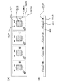
図1は、実施形態に係る半導体装置SDの構成を示す平面図である。図2は、図1のA−A´断面図である。なお、図2において、図を見やすくするために、外部接続端子SB及び電子部品ELP1の数は少なくなっている。
LABC>r+Ac+Ap・・・(1)
LBBC>r+Bc+Bp・・・(2)
LBBC>r+G+Bp・・・(3)
図15は、変形例1に係る半導体装置SDの構成を示す平面図である。図16は、図15に示した半導体装置SDからリッドLIDを取り除いた状態を示す平面図である。本変形例に係る半導体装置SDは、以下の点を除いて、実施形態に係る半導体装置SDと同様の構成である。
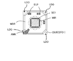
図23は、変形例2に係る半導体装置SDにおける配線基板ISUBの裏面SFC2を示す図である。本変形例に係る半導体装置SDは、裏面SFC2に、少なくとも一つの第2裏面電極AMK2(導体パターン)を有している点を除いて、実施形態に係る半導体装置SDと同様の構成である。
本変形例に係る半導体装置SDは、リッドLIDの代わりに封止樹脂MDRを有している。そして、第1半導体チップSC1は、ボンディングワイヤWIRを用いて配線基板ISUBに搭載されている。
AMK2 第2裏面電極(導体パターン)
BMP 端子
CNT 中央部
EDG 縁
EL 電極パッド
ELB 端子
ELP 電子部品
FNG 電極
HLD 保持治具
ISUB 配線基板
LDO 非被覆領域
LID リッド
LND 電極
MDR 封止樹脂
MINC 多層配線層
MMD 金型
OP 開口
PRJ 支持部
SB 外部接続端子
SC1 第1半導体チップ
SC2 第2半導体チップ
SD 半導体装置
SFC1 主面
SFC2 裏面
SFC3 主面
SFC4 裏面
SID1 第1辺
SID2 第2辺
SID3 第3辺
SID4 第4辺
SLP 傾斜部
SUB 基板
UFR1 アンダーフィル樹脂
UFR2 アンダーフィル樹脂
WIR ボンディングワイヤ
Claims (13)
- 第1面、前記第1面の反対側の第2面、および前記第1面上に形成された複数のバンプ電極を有する半導体チップと、
主面、および前記主面の反対側の裏面を有し、前記主面と前記半導体チップの前記第1面が対向するように、前記半導体チップが搭載された矩形状の配線基板と、
前記配線基板の前記主面及び前記半導体チップを覆い、前記主面上に接着材を介して固定された金属製のリッドと、
前記配線基板の前記裏面に配置された複数のはんだボールと、
前記配線基板の前記裏面に搭載され、且つ前記複数のはんだボールに囲まれた領域に配置された複数の電子部品と、
を備え、
前記リッドは、中央部、前記中央部の周辺に配置された周縁部、および前記中央部と前記周縁部を連続して接続する傾斜部を含み、
前記中央部と前記周縁部は、平面状に延在しており、
前記周縁部は、平面視において前記中央部を取り囲み、且つ前記中央部の周辺に沿って連続しており、
前記傾斜部は、前記配線基板に近づくように傾斜しており、
前記中央部は、平面視において4つの長辺と4つの短辺を有する8角形の形状を有しており、
前記中央部の4つの長辺のそれぞれは、平面視において前記配線基板の4つの辺のそれぞれと対向しており、
前記中央部の4つの短辺のそれぞれは、平面視において前記配線基板の4つの角のそれぞれと対向しており、
前記配線基板の4つの辺は、第1辺、第2辺、第3辺、および第4辺を含み、
前記配線基板の4つの角は、前記第1辺と前記第2辺とが交差する第1角、および前記第1角と対向し、且つ前記第3辺と前記第4辺とが交差する第2角、前記第1辺と前記第4辺とが交差する第3角、前記第3角と対向し、且つ前記第2辺と前記第3辺とが交差する第4角を含み、
前記中央部の4つの短辺は、前記第1角と対向する第1短辺、前記第2角と対向する第2短辺、前記第3角と対向する第3短辺、および前記第4角と対向する第4短辺を含み、
平面視において、前記配線基板の前記主面は、前記第1および第2辺と前記中央部の前記第1短辺に沿って延在する前記周縁部とで取り囲まれた第1領域、並びに前記第3および第4辺と前記中央部の前記第2短辺に沿って延在する前記周縁部とで取り囲まれた第2領域を有しており、
前記第1領域は、平面視において前記第2領域と対向しており、
前記第1および第2領域は、平面視において前記リッドで覆われておらず、
平面視において、前記リッドは、前記第1および前記第2領域を除き前記配線基板の前記主面の全面を実質的に覆っており、
平面視において前記第1領域に第1アライメントマークが配置されている半導体装置。 - 請求項1に記載の半導体装置において、
前記第1アライメントマークは、平面視において前記配線基板の第1辺と対向する第1辺、前記配線基板の前記第2辺に対向する第2辺、および前記リッドの前記周縁部と対向する第3辺を有している半導体装置。 - 請求項2に記載の半導体装置において、
平面視において、前記配線基板の前記主面上の前記リッドと重なり、且つ前記半導体チップの周りに配置された複数の第2アライメントマークを有する半導体装置。 - 請求項1に記載の半導体装置において、
前記配線基板は、平面視において前記裏面上に形成された複数の第3アライメントマークを有しており、
前記複数の第3アライメントマークは、平面視において前記複数のはんだボールに取り囲まれており、
前記複数の第3アライメントマークは、平面視において前記複数の電子部品の周りに配置されている半導体装置。 - 請求項4に記載の半導体装置において、
前記第1アライメントマークは、前記配線基板の前記主面上に形成された配線と同一の導体で形成されたパターンである半導体装置。 - 請求項1に記載の半導体装置において、
前記リッドの前記周縁部は、平面視において前記配線基板の前記第1辺と対向する第1縁部および前記配線基板の前記第2辺と対向する第2縁部を含み、
断面視において、前記第1縁部の第1幅は、前記第2辺の延在する第1方向において前記第1辺から前記第1縁部の端までの幅より大きく、
断面視において、前記第2縁部の第2幅は、前記第1方向と直交する第2方向において前記第2辺から前記第2縁部の端までの幅より大きく、
前記第2縁部の前記第2幅は、平面視において前記第1縁部の前記第1幅よりも大きい半導体装置。 - 第1面、前記第1面の反対側の第2面、および前記第1面上に形成された複数の第1バンプ電極を有する半導体チップと、
主面、および前記主面の反対側の裏面を有し、前記主面と前記半導体チップの前記第1面が対向するように、前記半導体チップが搭載されている矩形状の配線基板と、
前記配線基板の前記主面及び前記半導体チップを覆い、前記主面上に接着材を介して固定された金属製のリッドと、
前記配線基板の前記裏面に配置された複数のはんだボールと、
前記配線基板の前記裏面に搭載され、且つ前記複数のはんだボールに囲まれた領域に配置された複数の電子部品と、
を備え、
前記リッドは、中央部、前記中央部の周辺に配置された周縁部、および前記中央部と前記周縁部を連続して接続する傾斜部を含み、
前記中央部と前記周縁部は、平面状に延在し、
前記周縁部は、前記中央部を取り囲み、且つ前記中央部の周辺に沿って連続しており、
前記傾斜部は、前記配線基板に近づくように傾斜しており、
前記中央部は、平面視において4つの長辺と4つの短辺を有する8角形の形状を有しており、
前記中央部の4つの長辺のそれぞれは、平面視において前記配線基板の4つの辺のそれぞれと対向しており、
前記中央部の4つの短辺のそれぞれは、平面視において前記配線基板の4つの角のそれぞれと対向しており、
前記配線基板の4つの辺は、第1辺、第2辺、第3辺、および第4辺を含み、
前記配線基板の4つの角は、前記第1辺と前記第2辺とが交差する第1角、および前記第1角と対向し、且つ前記第3辺と前記第4辺とが交差する第2角、前記第1辺と前記第4辺とが交差する第3角、前記第3角と対向し、且つ前記第2辺と前記第3辺とが交差する第4角を含み、
前記中央部の4つの短辺は、前記第1角と対向する第1短辺、前記第2角と対向する第2短辺、前記第3角と対向する第3短辺、および前記第4角と対向する第4短辺を含み、
平面視において、前記配線基板の前記主面は、前記第1および第2辺と前記中央部の前記第1短辺に沿って延在する前記周縁部とで取り囲まれた第1領域、並びに前記第3および第4辺と前記中央部の前記第2短辺に沿って延在する前記周縁部とで取り囲まれた第2領域、前記第1および第4辺と前記中央部の前記第3短辺に沿って延在する前記周縁部とで取り囲まれた第3領域、並びに前記第2および第3辺と前記中央部の前記第4短辺に沿って延在する前記周縁部とで取り囲まれた第4領域を有しており、
前記第1領域は、平面視において前記第2領域と対向しており、
前記第3領域は、平面視において前記第4領域と対向しており、
前記第1、第2,第3および第4領域は、平面視において前記リッドで覆われておらず、
平面視において、前記リッドは、前記第1、第2、第3および第4領域を除き前記配線基板の前記主面の全面を実質的に覆っており、
平面視において前記第1、第2、第3および第4領域のうち少なくとも一つの領域に第1アライメントマークが配置されている半導体装置。 - 請求項7に記載の半導体装置において、
前記第1アライメントマークは、平面視において前記配線基板の第1辺と対向する第1辺、前記配線基板の前記第2辺に対向する第2辺、および前記リッドの前記周縁部と対向する第3辺を有している半導体装置。 - 請求項8に記載の半導体装置において、
平面視において、前記配線基板の前記主面上の前記リッドと重なり、且つ前記半導体チップの周りに配置された複数の第2アライメントマークを有する半導体装置。 - 請求項9に記載の半導体装置において、
前記配線基板は、平面視において前記裏面上に形成された複数の第3アライメントマークを有しており、
前記複数の第3アライメントマークは、平面視において前記複数のはんだボールに取り囲まれており、且つ前記複数の電子部品の周りに配置されている半導体装置。 - 請求項10に記載の半導体装置において、
前記第1アライメントマークは、前記配線基板の前記主面上に形成された配線と同一の導体で形成されたパターンである半導体装置。 - 請求項7に記載の半導体装置において、
前記リッドの前記周縁部は、平面視において前記配線基板の前記第1辺と対向する第1縁部および前記配線基板の前記第2辺と対向する第2縁部を含み、
断面視において、前記第1縁部の第1幅は、前記第2辺の延在する第1方向において前記第1辺から前記第1縁部の端までの幅より大きく、
断面視において、前記第2縁部の第2幅は、前記第1方向と直交する第2方向において前記第2辺から前記第2縁部の端までの幅より大きく、
前記第2縁部の前記第2幅は、平面視において前記第1縁部の前記第1幅よりも大きい半導体装置。 - 請求項1に記載の半導体装置において、
平面視において、
前記配線基板の前記第1角と前記第2角を結ぶ仮想の第1対角線と重なる前記リッドの前記周縁部から前記第1角までの前記第1領域上の幅は、前記配線基板の前記第3角と前記第4角を結ぶ仮想の第2対角線と重なる前記リッドの前記周縁部から前記第3角までの幅より大きい半導体装置。
Priority Applications (5)
| Application Number | Priority Date | Filing Date | Title |
|---|---|---|---|
| JP2013182363A JP6157998B2 (ja) | 2013-09-03 | 2013-09-03 | 半導体装置 |
| US14/447,181 US9142519B2 (en) | 2013-09-03 | 2014-07-30 | Semiconductor device with covering member that partially covers wiring substrate |
| CN201410446862.7A CN104517907A (zh) | 2013-09-03 | 2014-09-03 | 半导体器件 |
| US14/833,341 US20150364392A1 (en) | 2013-09-03 | 2015-08-24 | Semiconductor device with covering member that partially covers wiring substrate |
| HK15109477.6A HK1208958A1 (en) | 2013-09-03 | 2015-09-25 | Semiconductor device |
Applications Claiming Priority (1)
| Application Number | Priority Date | Filing Date | Title |
|---|---|---|---|
| JP2013182363A JP6157998B2 (ja) | 2013-09-03 | 2013-09-03 | 半導体装置 |
Publications (3)
| Publication Number | Publication Date |
|---|---|
| JP2015050384A JP2015050384A (ja) | 2015-03-16 |
| JP2015050384A5 JP2015050384A5 (ja) | 2016-03-24 |
| JP6157998B2 true JP6157998B2 (ja) | 2017-07-05 |
Family
ID=52582057
Family Applications (1)
| Application Number | Title | Priority Date | Filing Date |
|---|---|---|---|
| JP2013182363A Active JP6157998B2 (ja) | 2013-09-03 | 2013-09-03 | 半導体装置 |
Country Status (4)
| Country | Link |
|---|---|
| US (2) | US9142519B2 (ja) |
| JP (1) | JP6157998B2 (ja) |
| CN (1) | CN104517907A (ja) |
| HK (1) | HK1208958A1 (ja) |
Families Citing this family (8)
| Publication number | Priority date | Publication date | Assignee | Title |
|---|---|---|---|---|
| WO2016044179A2 (en) * | 2014-09-15 | 2016-03-24 | Invensas Corporation | Electronic structures strengthened by porous and non-porous layers, and methods of fabrication |
| TWI545714B (zh) * | 2015-03-06 | 2016-08-11 | 矽品精密工業股份有限公司 | 電子封裝件及其製法 |
| US10607958B2 (en) * | 2015-08-28 | 2020-03-31 | Texas Instruments Incorporated | Flip chip backside die grounding techniques |
| WO2018088293A1 (ja) | 2016-11-14 | 2018-05-17 | 株式会社村田製作所 | 電子部品及び三端子コンデンサ |
| KR102633142B1 (ko) * | 2019-08-26 | 2024-02-02 | 삼성전자주식회사 | 반도체 패키지 |
| FR3109466B1 (fr) * | 2020-04-16 | 2024-05-17 | St Microelectronics Grenoble 2 | Dispositif de support d’une puce électronique et procédé de fabrication correspondant |
| KR20210150658A (ko) * | 2020-06-03 | 2021-12-13 | 삼성전자주식회사 | 반도체 패키지 |
| JP7528557B2 (ja) * | 2020-06-19 | 2024-08-06 | 日本電気株式会社 | 量子デバイス及びその製造方法 |
Family Cites Families (17)
| Publication number | Priority date | Publication date | Assignee | Title |
|---|---|---|---|---|
| JP2851745B2 (ja) | 1992-03-27 | 1999-01-27 | 京セラ株式会社 | 電子部品収納用パッケージ |
| US5789810A (en) * | 1995-12-21 | 1998-08-04 | International Business Machines Corporation | Semiconductor cap |
| JPH10270815A (ja) * | 1997-03-21 | 1998-10-09 | Ngk Spark Plug Co Ltd | 配線基板及びその製造方法 |
| US5898219A (en) * | 1997-04-02 | 1999-04-27 | Intel Corporation | Custom corner attach heat sink design for a plastic ball grid array integrated circuit package |
| JP2861981B2 (ja) * | 1997-04-11 | 1999-02-24 | 日本電気株式会社 | 半導体装置の冷却構造 |
| JP3834426B2 (ja) * | 1997-09-02 | 2006-10-18 | 沖電気工業株式会社 | 半導体装置 |
| JP3462979B2 (ja) * | 1997-12-01 | 2003-11-05 | 株式会社東芝 | 半導体装置 |
| TW388976B (en) * | 1998-10-21 | 2000-05-01 | Siliconware Precision Industries Co Ltd | Semiconductor package with fully exposed heat sink |
| US6218730B1 (en) * | 1999-01-06 | 2001-04-17 | International Business Machines Corporation | Apparatus for controlling thermal interface gap distance |
| JP3467454B2 (ja) * | 2000-06-05 | 2003-11-17 | Necエレクトロニクス株式会社 | 半導体装置の製造方法 |
| KR100375720B1 (ko) * | 2000-10-09 | 2003-03-15 | 삼성전자주식회사 | 반도체 패키지 및 그의 제조 방법 |
| US6653730B2 (en) * | 2000-12-14 | 2003-11-25 | Intel Corporation | Electronic assembly with high capacity thermal interface |
| JP4473141B2 (ja) * | 2005-01-04 | 2010-06-02 | 日立オートモティブシステムズ株式会社 | 電子制御装置 |
| JP4768314B2 (ja) * | 2005-05-16 | 2011-09-07 | 株式会社東芝 | 半導体装置 |
| JP2007042719A (ja) | 2005-08-01 | 2007-02-15 | Nec Electronics Corp | 半導体装置 |
| US8202765B2 (en) * | 2009-01-22 | 2012-06-19 | International Business Machines Corporation | Achieving mechanical and thermal stability in a multi-chip package |
| JP2012054597A (ja) | 2011-11-07 | 2012-03-15 | Renesas Electronics Corp | 半導体装置 |
-
2013
- 2013-09-03 JP JP2013182363A patent/JP6157998B2/ja active Active
-
2014
- 2014-07-30 US US14/447,181 patent/US9142519B2/en not_active Expired - Fee Related
- 2014-09-03 CN CN201410446862.7A patent/CN104517907A/zh active Pending
-
2015
- 2015-08-24 US US14/833,341 patent/US20150364392A1/en not_active Abandoned
- 2015-09-25 HK HK15109477.6A patent/HK1208958A1/xx unknown
Also Published As
| Publication number | Publication date |
|---|---|
| CN104517907A (zh) | 2015-04-15 |
| US20150364392A1 (en) | 2015-12-17 |
| JP2015050384A (ja) | 2015-03-16 |
| US9142519B2 (en) | 2015-09-22 |
| US20150061104A1 (en) | 2015-03-05 |
| HK1208958A1 (en) | 2016-03-18 |
Similar Documents
| Publication | Publication Date | Title |
|---|---|---|
| JP6157998B2 (ja) | 半導体装置 | |
| US10431556B2 (en) | Semiconductor device including semiconductor chips mounted over both surfaces of substrate | |
| US10734367B2 (en) | Semiconductor package and method of fabricating the same | |
| KR102591624B1 (ko) | 반도체 패키지 | |
| US8710647B2 (en) | Semiconductor device having a first conductive member connecting a chip to a wiring board pad and a second conductive member connecting the wiring board pad to a land on an insulator covering the chip and the wiring board | |
| JP6110734B2 (ja) | 半導体装置 | |
| US10971425B2 (en) | Semiconductor device | |
| US9054093B2 (en) | Semiconductor device | |
| US20150102484A1 (en) | Package structure and fabrication method thereof | |
| JP2011155203A (ja) | 半導体装置 | |
| JP2010147070A (ja) | 半導体装置 | |
| JP2002231859A (ja) | 半導体装置、及び、半導体装置の製造方法 | |
| US20090196003A1 (en) | Wiring board for semiconductor devices, semiconductor device, electronic device, and motherboard | |
| JP2012099610A (ja) | 配線基板およびその製造方法、並びに半導体パッケージの製造方法 | |
| JP2009111279A (ja) | 半導体装置の配線基板、半導体装置、電子装置、マザーボード、半導体装置の配線基板の製造方法、マザーボードの製造方法、電子装置の製造方法 | |
| JP4556671B2 (ja) | 半導体パッケージ及びフレキシブルサーキット基板 | |
| KR101376396B1 (ko) | 반도체 디바이스 및 그 제조 방법 | |
| JP2004247464A (ja) | 半導体装置及びその製造方法 | |
| EP3182449A1 (en) | Semiconductor package | |
| JP2006147921A (ja) | 半導体装置及びその製造方法 | |
| US8039941B2 (en) | Circuit board, lead frame, semiconductor device, and method for fabricating the same | |
| WO2014103855A1 (ja) | 半導体装置およびその製造方法 | |
| JP2014236197A (ja) | 半導体装置 | |
| KR101096457B1 (ko) | 멀티 패키지 | |
| JP2014236196A (ja) | 半導体装置 |
Legal Events
| Date | Code | Title | Description |
|---|---|---|---|
| A521 | Request for written amendment filed |
Free format text: JAPANESE INTERMEDIATE CODE: A523 Effective date: 20160202 |
|
| A621 | Written request for application examination |
Free format text: JAPANESE INTERMEDIATE CODE: A621 Effective date: 20160202 |
|
| A977 | Report on retrieval |
Free format text: JAPANESE INTERMEDIATE CODE: A971007 Effective date: 20161216 |
|
| A131 | Notification of reasons for refusal |
Free format text: JAPANESE INTERMEDIATE CODE: A131 Effective date: 20161227 |
|
| A521 | Request for written amendment filed |
Free format text: JAPANESE INTERMEDIATE CODE: A523 Effective date: 20170208 |
|
| TRDD | Decision of grant or rejection written | ||
| A01 | Written decision to grant a patent or to grant a registration (utility model) |
Free format text: JAPANESE INTERMEDIATE CODE: A01 Effective date: 20170530 |
|
| A61 | First payment of annual fees (during grant procedure) |
Free format text: JAPANESE INTERMEDIATE CODE: A61 Effective date: 20170607 |
|
| R150 | Certificate of patent or registration of utility model |
Ref document number: 6157998 Country of ref document: JP Free format text: JAPANESE INTERMEDIATE CODE: R150 |