JP6144098B2 - プログラマブルlsi - Google Patents
プログラマブルlsi Download PDFInfo
- Publication number
- JP6144098B2 JP6144098B2 JP2013091916A JP2013091916A JP6144098B2 JP 6144098 B2 JP6144098 B2 JP 6144098B2 JP 2013091916 A JP2013091916 A JP 2013091916A JP 2013091916 A JP2013091916 A JP 2013091916A JP 6144098 B2 JP6144098 B2 JP 6144098B2
- Authority
- JP
- Japan
- Prior art keywords
- transistor
- film
- oxide
- electrically connected
- insulating film
- Prior art date
- Legal status (The legal status is an assumption and is not a legal conclusion. Google has not performed a legal analysis and makes no representation as to the accuracy of the status listed.)
- Expired - Fee Related
Links
Images


Classifications
-
- H—ELECTRICITY
- H03—ELECTRONIC CIRCUITRY
- H03K—PULSE TECHNIQUE
- H03K19/00—Logic circuits, i.e. having at least two inputs acting on one output; Inverting circuits
- H03K19/02—Logic circuits, i.e. having at least two inputs acting on one output; Inverting circuits using specified components
- H03K19/173—Logic circuits, i.e. having at least two inputs acting on one output; Inverting circuits using specified components using elementary logic circuits as components
-
- H—ELECTRICITY
- H03—ELECTRONIC CIRCUITRY
- H03K—PULSE TECHNIQUE
- H03K19/00—Logic circuits, i.e. having at least two inputs acting on one output; Inverting circuits
- H03K19/0008—Arrangements for reducing power consumption
- H03K19/0013—Arrangements for reducing power consumption in field effect transistor circuits
-
- H—ELECTRICITY
- H03—ELECTRONIC CIRCUITRY
- H03K—PULSE TECHNIQUE
- H03K19/00—Logic circuits, i.e. having at least two inputs acting on one output; Inverting circuits
- H03K19/02—Logic circuits, i.e. having at least two inputs acting on one output; Inverting circuits using specified components
- H03K19/173—Logic circuits, i.e. having at least two inputs acting on one output; Inverting circuits using specified components using elementary logic circuits as components
- H03K19/177—Logic circuits, i.e. having at least two inputs acting on one output; Inverting circuits using specified components using elementary logic circuits as components arranged in matrix form
- H03K19/1778—Structural details for adapting physical parameters
- H03K19/17784—Structural details for adapting physical parameters for supply voltage
-
- H—ELECTRICITY
- H03—ELECTRONIC CIRCUITRY
- H03K—PULSE TECHNIQUE
- H03K19/00—Logic circuits, i.e. having at least two inputs acting on one output; Inverting circuits
- H03K19/02—Logic circuits, i.e. having at least two inputs acting on one output; Inverting circuits using specified components
- H03K19/173—Logic circuits, i.e. having at least two inputs acting on one output; Inverting circuits using specified components using elementary logic circuits as components
- H03K19/177—Logic circuits, i.e. having at least two inputs acting on one output; Inverting circuits using specified components using elementary logic circuits as components arranged in matrix form
- H03K19/1778—Structural details for adapting physical parameters
- H03K19/17792—Structural details for adapting physical parameters for operating speed
Landscapes
- Physics & Mathematics (AREA)
- Mathematical Physics (AREA)
- Engineering & Computer Science (AREA)
- Computer Hardware Design (AREA)
- Computing Systems (AREA)
- General Engineering & Computer Science (AREA)
- Thin Film Transistor (AREA)
- Logic Circuits (AREA)
- Static Random-Access Memory (AREA)
- Dram (AREA)
- Semiconductor Integrated Circuits (AREA)
Description
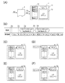
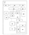
図1(A)は、本発明の一態様に係るプログラマブルLSI1の構成例を示す図である。プログラマブルLSI1は、コンフィギュレーションデータ(CD_x)を保持することが可能なコンフィギュレーションメモリ11と、コンフィギュレーションメモリ11に保持されるコンフィギュレーションデータ(CD_x)に基づいて回路構成(LC(CD_x))が決定される論理回路部12とを有する。さらに、プログラマブルLSI1は、それぞれにおいてコンフィギュレーションデータ(CD)を格納することが可能な複数のバンク(Bank_1〜Bank_n)(バンク群10ともいう)を有する。
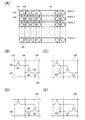
図2(A)は、図1(A)に示すバンク群10の構成例を示す図である。図2(A)に示すバンク群10は、マトリクス状に配設されている複数のメモリセル100と、それぞれが特定の一列に配設されているメモリセル100の全てに電気的に接続されている複数の入力ビット線110と、それぞれが特定の一列に配設されているメモリセル100の全てに電気的に接続されている複数の出力ビット線120と、それぞれが特定の一行に配設されているメモリセル100の全てに電気的に接続されている複数の入力ワード線130と、それぞれが特定の一行に配設されているメモリセル100の全てに電気的に接続されている複数の出力ワード線140と、を有する。
図2(B)〜(E)は、図2(A)に示すメモリセル100の構成例を示す回路図である。
上述したメモリセル100の構造例について説明する。具体的には、図2(C)に示すトランジスタ101及びトランジスタ102並びにキャパシタ104の構造例及びその作製方法例について説明する。なお、以下では、トランジスタ101としてチャネルが酸化物半導体層に形成されるトランジスタを適用し、トランジスタ102としてチャネルが単結晶シリコン層に形成されるトランジスタを適用する場合について説明する。なお、図2(C)に示すトランジスタ103は、トランジスタ102と同様に作製することができる。
論理回路部12は、複数のロジックエレメントと、ロジックエレメント間の配線とで構成される。各ロジックエレメントの機能を変更することで、論理回路部12の機能を変更することができる。また、ロジックエレメント間の配線の電気的な接続関係を変更することで、論理回路部12の機能を変更することができる。
スイッチ600は、論理回路部12におけるロジックエレメント612とロジックエレメント618との接続を制御する。そして、図9に示すロジックエレメント612、ロジックエレメント618はそれぞれ、ルックアップテーブル613、619、フリップフロップ614、620、AND回路615、621により構成されている。
2 コンパイラ
10 バンク群
11 コンフィギュレーションメモリ
12 論理回路部
100 メモリセル
101 トランジスタ
102 トランジスタ
103 トランジスタ
104 キャパシタ
110 入力ビット線
120 出力ビット線
130 入力ワード線
140 出力ワード線
150 基準電位線
421 RF回路
422 アナログベースバンド回路
423 デジタルベースバンド回路
424 バッテリー
425 電源回路
426 アプリケーションプロセッサ
427 CPU
428 DSP
429 インターフェース
430 フラッシュメモリ
431 ディスプレイコントローラ
432 メモリ回路
433 ディスプレイ
434 表示部
435 ソースドライバ
436 ゲートドライバ
437 音声回路
438 キーボード
439 タッチセンサ
451 バッテリー
452 電源回路
453 マイクロプロセッサ
454 フラッシュメモリ
455 音声回路
456 キーボード
457 メモリ回路
458 タッチパネル
459 ディスプレイ
460 ディスプレイコントローラ
600 スイッチ
601a トランジスタ
601b トランジスタ
601c トランジスタ
602a トランジスタ
602b トランジスタ
602c トランジスタ
603a ノード
603b ノード
603c ノード
605a 配線
605b 配線
605c 配線
606a 配線
606b 配線
606c 配線
607 配線
608a トランジスタ
608b トランジスタ
608c トランジスタ
610 配線
611 配線
612 ロジックエレメント
613 ルックアップテーブル
614 フリップフロップ
615 AND回路
618 ロジックエレメント
619 ルックアップテーブル
620 フリップフロップ
621 AND回路
630 組
631 組
632 組
700 基板
701 絶縁膜
702 半導体膜
703 ゲート絶縁膜
707 ゲート電極
709 不純物領域
710 チャネル形成領域
712 絶縁膜
713 絶縁膜
716 酸化物半導体層
719 導電膜
720 導電膜
721 ゲート絶縁膜
722 ゲート電極
723 導電膜
724 絶縁膜
725 開口部
726 配線
727 絶縁膜
Claims (6)
- 論理回路部と、
コンフィグレーションデータを保持することで前記論理回路部の構成を決定するコンフィグレーションメモリと、
複数のコンフィグレーションデータを格納することが可能なバンク群と、を有し、
外部から供給されるタイムスケジュールに基づいて、前記バンク群に、外部から供給される複数のコンフィグレーションデータを逐次格納する動作と、
前記タイムスケジュールに基づいて、前記コンフィグレーションメモリを、前記バンク群に格納されている複数のコンフィグレーションデータの一と書き換える動作と、を有し、
前記格納する動作と、前記書き換える動作とを、前記論理回路部の動作が継続中に、独立且つ併行して行うことを特徴とするプログラマブルLSI。 - 前記バンク群は、マトリクス状に配設された複数のメモリセルを有し、
前記メモリセルは、
入力ワード線と、
出力ワード線と、
基準電位線と、
ゲートが前記入力ワード線に電気的に接続され、ソース及びドレインの一方が前記入力ビット線に電気的に接続されている第1のトランジスタと、
ゲートが前記第1のトランジスタのソース及びドレインの他方に電気的に接続され、ソース及びドレインの一方が前記基準電位線に電気的に接続されている第2のトランジスタと、
ゲートが前記出力ワード線に電気的に接続され、ソース及びドレインの一方が前記第2のトランジスタのソース及びドレインの他方に電気的に接続され、ソース及びドレインの他方が前記出力ビット線に電気的に接続されている第3のトランジスタと、を有することを特徴とする請求項1に記載のプログラマブルLSI。 - 前記バンク群は、マトリクス状に配設された複数のメモリセルを有し、
前記メモリセルは、
入力ワード線と、
出力ワード線と、
基準電位線と、
ゲートが前記入力ワード線に電気的に接続され、ソース及びドレインの一方が前記入力ビット線に電気的に接続されている第1のトランジスタと、
ゲートが前記出力ワード線に電気的に接続され、ソース及びドレインの一方が前記基準電位線に電気的に接続されている第2のトランジスタと、
ゲートが前記第1のトランジスタのソース及びドレインの他方に電気的に接続され、ソース及びドレインの一方が前記第2のトランジスタのソース及びドレインの他方に電気的に接続され、ソース及びドレインの他方が前記出力ビット線に電気的に接続されている第3のトランジスタと、を有することを特徴とする請求項1に記載のプログラマブルLSI。 - 前記メモリセルは、
一方の電極が前記第1のトランジスタのソース及びドレインの他方に電気的に接続され、他方の電極が接地されているキャパシタを有することを特徴とする請求項2又は請求項3に記載のプログラマブルLSI。 - 前記第1のトランジスタは、チャネルとして酸化物半導体層を有することを特徴とする請求項2乃至請求項4のいずれか一項に記載のプログラマブルLSI。
- 前記メモリセルは、多値のデータを格納することが可能であることを特徴とする請求項2乃至請求項5のいずれか一項に記載のプログラマブルLSI。
Priority Applications (1)
| Application Number | Priority Date | Filing Date | Title |
|---|---|---|---|
| JP2013091916A JP6144098B2 (ja) | 2012-04-27 | 2013-04-25 | プログラマブルlsi |
Applications Claiming Priority (3)
| Application Number | Priority Date | Filing Date | Title |
|---|---|---|---|
| JP2012102014 | 2012-04-27 | ||
| JP2012102014 | 2012-04-27 | ||
| JP2013091916A JP6144098B2 (ja) | 2012-04-27 | 2013-04-25 | プログラマブルlsi |
Publications (3)
| Publication Number | Publication Date |
|---|---|
| JP2013243657A JP2013243657A (ja) | 2013-12-05 |
| JP2013243657A5 JP2013243657A5 (ja) | 2016-05-26 |
| JP6144098B2 true JP6144098B2 (ja) | 2017-06-07 |
Family
ID=49323418
Family Applications (1)
| Application Number | Title | Priority Date | Filing Date |
|---|---|---|---|
| JP2013091916A Expired - Fee Related JP6144098B2 (ja) | 2012-04-27 | 2013-04-25 | プログラマブルlsi |
Country Status (4)
| Country | Link |
|---|---|
| US (1) | US9654107B2 (ja) |
| JP (1) | JP6144098B2 (ja) |
| KR (1) | KR102047553B1 (ja) |
| DE (1) | DE102013207217A1 (ja) |
Families Citing this family (35)
| Publication number | Priority date | Publication date | Assignee | Title |
|---|---|---|---|---|
| KR101978932B1 (ko) | 2012-05-02 | 2019-05-16 | 가부시키가이샤 한도오따이 에네루기 켄큐쇼 | 프로그램 가능한 로직 디바이스 |
| CN104321967B (zh) | 2012-05-25 | 2018-01-09 | 株式会社半导体能源研究所 | 可编程逻辑装置及半导体装置 |
| JP6377317B2 (ja) | 2012-05-30 | 2018-08-22 | 株式会社半導体エネルギー研究所 | プログラマブルロジックデバイス |
| KR102102589B1 (ko) | 2012-10-17 | 2020-04-22 | 가부시키가이샤 한도오따이 에네루기 켄큐쇼 | 프로그램 가능한 논리 장치 |
| KR102112364B1 (ko) | 2012-12-06 | 2020-05-18 | 가부시키가이샤 한도오따이 에네루기 켄큐쇼 | 반도체 장치 |
| TWI611419B (zh) * | 2012-12-24 | 2018-01-11 | 半導體能源研究所股份有限公司 | 可程式邏輯裝置及半導體裝置 |
| US8952723B2 (en) | 2013-02-13 | 2015-02-10 | Semiconductor Energy Laboratory Co., Ltd. | Programmable logic device and semiconductor device |
| WO2014125979A1 (en) | 2013-02-13 | 2014-08-21 | Semiconductor Energy Laboratory Co., Ltd. | Programmable logic device and semiconductor device |
| US8947121B2 (en) | 2013-03-12 | 2015-02-03 | Semiconductor Energy Laboratory Co., Ltd. | Programmable logic device |
| JP6272713B2 (ja) | 2013-03-25 | 2018-01-31 | 株式会社半導体エネルギー研究所 | プログラマブルロジックデバイス及び半導体装置 |
| TWI621337B (zh) | 2013-05-14 | 2018-04-11 | 半導體能源研究所股份有限公司 | 信號處理裝置 |
| US9172369B2 (en) | 2013-05-17 | 2015-10-27 | Semiconductor Energy Laboratory Co., Ltd. | Programmable logic device and semiconductor device |
| JP6368155B2 (ja) | 2013-06-18 | 2018-08-01 | 株式会社半導体エネルギー研究所 | プログラマブルロジックデバイス |
| JP6352070B2 (ja) | 2013-07-05 | 2018-07-04 | 株式会社半導体エネルギー研究所 | 半導体装置 |
| JP6483402B2 (ja) | 2013-11-01 | 2019-03-13 | 株式会社半導体エネルギー研究所 | 記憶装置、及び記憶装置を有する電子機器 |
| JP6478562B2 (ja) | 2013-11-07 | 2019-03-06 | 株式会社半導体エネルギー研究所 | 半導体装置 |
| JP6393590B2 (ja) | 2013-11-22 | 2018-09-19 | 株式会社半導体エネルギー研究所 | 半導体装置 |
| JP6444723B2 (ja) | 2014-01-09 | 2018-12-26 | 株式会社半導体エネルギー研究所 | 装置 |
| US9379713B2 (en) | 2014-01-17 | 2016-06-28 | Semiconductor Energy Laboratory Co., Ltd. | Data processing device and driving method thereof |
| JP6521643B2 (ja) | 2014-01-24 | 2019-05-29 | 株式会社半導体エネルギー研究所 | 半導体装置 |
| US9721968B2 (en) | 2014-02-06 | 2017-08-01 | Semiconductor Energy Laboratory Co., Ltd. | Semiconductor device, electronic component, and electronic appliance |
| WO2015118436A1 (en) | 2014-02-07 | 2015-08-13 | Semiconductor Energy Laboratory Co., Ltd. | Semiconductor device, device, and electronic device |
| JP2015165226A (ja) | 2014-02-07 | 2015-09-17 | 株式会社半導体エネルギー研究所 | 装置 |
| US9869716B2 (en) | 2014-02-07 | 2018-01-16 | Semiconductor Energy Laboratory Co., Ltd. | Device comprising programmable logic element |
| JP6442321B2 (ja) | 2014-03-07 | 2018-12-19 | 株式会社半導体エネルギー研究所 | 半導体装置及びその駆動方法、並びに電子機器 |
| JP6677449B2 (ja) * | 2014-03-13 | 2020-04-08 | 株式会社半導体エネルギー研究所 | 半導体装置の駆動方法 |
| JP6541376B2 (ja) | 2014-03-13 | 2019-07-10 | 株式会社半導体エネルギー研究所 | プログラマブルロジックデバイスの動作方法 |
| TWI643457B (zh) | 2014-04-25 | 2018-12-01 | 日商半導體能源研究所股份有限公司 | 半導體裝置 |
| JP6645793B2 (ja) | 2014-10-17 | 2020-02-14 | 株式会社半導体エネルギー研究所 | 半導体装置 |
| WO2016092416A1 (en) * | 2014-12-11 | 2016-06-16 | Semiconductor Energy Laboratory Co., Ltd. | Semiconductor device, memory device, and electronic device |
| JP2017102904A (ja) * | 2015-10-23 | 2017-06-08 | 株式会社半導体エネルギー研究所 | 半導体装置および電子機器 |
| KR102643895B1 (ko) | 2015-10-30 | 2024-03-05 | 가부시키가이샤 한도오따이 에네루기 켄큐쇼 | 반도체 장치, 전자 부품, 및 전자 기기 |
| KR20180081732A (ko) | 2015-11-13 | 2018-07-17 | 가부시키가이샤 한도오따이 에네루기 켄큐쇼 | 반도체 장치, 전자 부품, 및 전자 기기 |
| US9998119B2 (en) | 2016-05-20 | 2018-06-12 | Semiconductor Energy Laboratory Co., Ltd. | Semiconductor device, electronic component, and electronic device |
| DE112017004148T5 (de) | 2016-08-19 | 2019-05-23 | Semiconductor Energy Laboratory Co., Ltd. | Verfahren zum Steuern der Stromzufuhr in einer Halbleitervorrichtung |
Family Cites Families (37)
| Publication number | Priority date | Publication date | Assignee | Title |
|---|---|---|---|---|
| US4870302A (en) | 1984-03-12 | 1989-09-26 | Xilinx, Inc. | Configurable electrical circuit having configurable logic elements and configurable interconnects |
| US4609986A (en) | 1984-06-14 | 1986-09-02 | Altera Corporation | Programmable logic array device using EPROM technology |
| US4642487A (en) | 1984-09-26 | 1987-02-10 | Xilinx, Inc. | Special interconnect for configurable logic array |
| JPH0563551A (ja) | 1991-08-29 | 1993-03-12 | Kawasaki Steel Corp | プログラマブル論理回路装置 |
| JP4103968B2 (ja) | 1996-09-18 | 2008-06-18 | 株式会社半導体エネルギー研究所 | 絶縁ゲイト型半導体装置 |
| JP3106998B2 (ja) | 1997-04-11 | 2000-11-06 | 日本電気株式会社 | メモリ付加型プログラマブルロジックlsi |
| WO2002037264A2 (en) * | 2000-11-06 | 2002-05-10 | Broadcom Corporation | Reconfigurable processing system and method |
| JP2003122638A (ja) * | 2001-10-18 | 2003-04-25 | Fujitsu Ltd | 半導体集積回路装置 |
| US7221586B2 (en) * | 2002-07-08 | 2007-05-22 | Micron Technology, Inc. | Memory utilizing oxide nanolaminates |
| US7088606B2 (en) * | 2004-03-10 | 2006-08-08 | Altera Corporation | Dynamic RAM storage techniques |
| ITMI20041675A1 (it) * | 2004-08-30 | 2004-11-30 | St Microelectronics Srl | Blocco di commutazione e relativa matrice di commutazione, in particolare per architetture fpga. |
| JP2006287675A (ja) | 2005-04-01 | 2006-10-19 | Renesas Technology Corp | 半導体集積回路 |
| US7793040B2 (en) * | 2005-06-01 | 2010-09-07 | Microsoft Corporation | Content addressable memory architecture |
| EP1998373A3 (en) | 2005-09-29 | 2012-10-31 | Semiconductor Energy Laboratory Co, Ltd. | Semiconductor device having oxide semiconductor layer and manufacturing method thereof |
| JP2007251329A (ja) | 2006-03-14 | 2007-09-27 | Matsushita Electric Ind Co Ltd | プログラマブルロジックデバイス |
| JP4866194B2 (ja) | 2006-09-29 | 2012-02-01 | 富士通セミコンダクター株式会社 | 集積回路及びリコンフィギュラブル回路の入力データ制御方法 |
| JP2008152409A (ja) | 2006-12-15 | 2008-07-03 | Renesas Technology Corp | 半導体集積回路 |
| JP4847585B2 (ja) | 2007-06-12 | 2011-12-28 | 富士通株式会社 | コンフィグレーション装置 |
| US7928761B2 (en) * | 2007-09-06 | 2011-04-19 | Tabula, Inc. | Configuration context switcher with a latch |
| JP2009129046A (ja) * | 2007-11-21 | 2009-06-11 | Panasonic Corp | リコンフィギュラブル回路,リコンフィギュラブル回路の機能変更方法および通信装置 |
| JP5781720B2 (ja) | 2008-12-15 | 2015-09-24 | ルネサスエレクトロニクス株式会社 | 半導体装置及び半導体装置の製造方法 |
| KR101581882B1 (ko) * | 2009-04-20 | 2015-12-31 | 삼성전자주식회사 | 재구성 가능한 프로세서 및 그 재구성 방법 |
| US8359448B1 (en) * | 2009-07-17 | 2013-01-22 | Xilinx, Inc. | Specific memory controller implemented using reconfiguration |
| CN102612741B (zh) | 2009-11-06 | 2014-11-12 | 株式会社半导体能源研究所 | 半导体装置 |
| MY187143A (en) | 2010-01-20 | 2021-09-03 | Semiconductor Energy Lab | Semiconductor device |
| JP5735503B2 (ja) | 2010-06-24 | 2015-06-17 | 太陽誘電株式会社 | 半導体装置 |
| KR20120036208A (ko) * | 2010-10-07 | 2012-04-17 | 삼성전자주식회사 | 재구성 기반 컴퓨팅 장치 및 이의 메모리 의존성 보정방법 |
| KR101899880B1 (ko) | 2011-02-17 | 2018-09-18 | 가부시키가이샤 한도오따이 에네루기 켄큐쇼 | 프로그래머블 lsi |
| US8542032B1 (en) * | 2012-01-06 | 2013-09-24 | Altera Corporation | Integrated circuits with interconnect selection circuitry |
| JP5613694B2 (ja) | 2012-01-19 | 2014-10-29 | ユーオーピー エルエルシー | 結晶性アルミノシリケートゼオライト質組成物:uzm−15 |
| JP6125850B2 (ja) | 2012-02-09 | 2017-05-10 | 株式会社半導体エネルギー研究所 | 半導体装置及び半導体装置の作製方法 |
| KR101978932B1 (ko) | 2012-05-02 | 2019-05-16 | 가부시키가이샤 한도오따이 에네루기 켄큐쇼 | 프로그램 가능한 로직 디바이스 |
| JP6377317B2 (ja) | 2012-05-30 | 2018-08-22 | 株式会社半導体エネルギー研究所 | プログラマブルロジックデバイス |
| JP2014030110A (ja) * | 2012-07-31 | 2014-02-13 | Toshiba Corp | リコンフィギャラブル集積回路装置およびその書き込み方法 |
| US9323544B2 (en) * | 2013-10-09 | 2016-04-26 | International Business Machines Corporation | Dynamic reconfiguration of queue pairs |
| US9727460B2 (en) * | 2013-11-01 | 2017-08-08 | Samsung Electronics Co., Ltd. | Selecting a memory mapping scheme by determining a number of functional units activated in each cycle of a loop based on analyzing parallelism of a loop |
| KR102149509B1 (ko) * | 2014-03-27 | 2020-08-28 | 삼성전자주식회사 | 구성 데이터를 압축 및 복원하는 방법 |
-
2013
- 2013-04-17 US US13/864,461 patent/US9654107B2/en active Active
- 2013-04-22 DE DE102013207217A patent/DE102013207217A1/de not_active Withdrawn
- 2013-04-24 KR KR1020130045208A patent/KR102047553B1/ko not_active Expired - Fee Related
- 2013-04-25 JP JP2013091916A patent/JP6144098B2/ja not_active Expired - Fee Related
Also Published As
| Publication number | Publication date |
|---|---|
| JP2013243657A (ja) | 2013-12-05 |
| KR102047553B1 (ko) | 2019-11-21 |
| US9654107B2 (en) | 2017-05-16 |
| KR20130121730A (ko) | 2013-11-06 |
| DE102013207217A1 (de) | 2013-10-31 |
| US20130285697A1 (en) | 2013-10-31 |
Similar Documents
| Publication | Publication Date | Title |
|---|---|---|
| JP6144098B2 (ja) | プログラマブルlsi | |
| KR101899881B1 (ko) | 프로그래머블 lsi | |
| JP6488037B2 (ja) | 半導体装置 | |
| JP5859839B2 (ja) | 記憶素子の駆動方法、及び、記憶素子 | |
| JP6223668B2 (ja) | 半導体装置 | |
| KR20120075411A (ko) | 신호 처리 회로 | |
| JP6145140B2 (ja) | 信号処理回路の作製方法 | |
| JP6031252B2 (ja) | 半導体装置、記憶装置および半導体装置の作製方法 | |
| JP2012238372A (ja) | 半導体記憶装置 | |
| US8630110B2 (en) | Semiconductor memory device |
Legal Events
| Date | Code | Title | Description |
|---|---|---|---|
| A521 | Request for written amendment filed |
Free format text: JAPANESE INTERMEDIATE CODE: A523 Effective date: 20160330 |
|
| A621 | Written request for application examination |
Free format text: JAPANESE INTERMEDIATE CODE: A621 Effective date: 20160330 |
|
| A977 | Report on retrieval |
Free format text: JAPANESE INTERMEDIATE CODE: A971007 Effective date: 20161226 |
|
| A131 | Notification of reasons for refusal |
Free format text: JAPANESE INTERMEDIATE CODE: A131 Effective date: 20170110 |
|
| A521 | Request for written amendment filed |
Free format text: JAPANESE INTERMEDIATE CODE: A523 Effective date: 20170302 |
|
| TRDD | Decision of grant or rejection written | ||
| A01 | Written decision to grant a patent or to grant a registration (utility model) |
Free format text: JAPANESE INTERMEDIATE CODE: A01 Effective date: 20170418 |
|
| A61 | First payment of annual fees (during grant procedure) |
Free format text: JAPANESE INTERMEDIATE CODE: A61 Effective date: 20170510 |
|
| R150 | Certificate of patent or registration of utility model |
Ref document number: 6144098 Country of ref document: JP Free format text: JAPANESE INTERMEDIATE CODE: R150 |
|
| R250 | Receipt of annual fees |
Free format text: JAPANESE INTERMEDIATE CODE: R250 |
|
| LAPS | Cancellation because of no payment of annual fees |