JP6000560B2 - Semiconductor memory device - Google Patents
Semiconductor memory device Download PDFInfo
- Publication number
- JP6000560B2 JP6000560B2 JP2012019406A JP2012019406A JP6000560B2 JP 6000560 B2 JP6000560 B2 JP 6000560B2 JP 2012019406 A JP2012019406 A JP 2012019406A JP 2012019406 A JP2012019406 A JP 2012019406A JP 6000560 B2 JP6000560 B2 JP 6000560B2
- Authority
- JP
- Japan
- Prior art keywords
- bit line
- sub
- semiconductor
- capacitor
- potential
- Prior art date
- Legal status (The legal status is an assumption and is not a legal conclusion. Google has not performed a legal analysis and makes no representation as to the accuracy of the status listed.)
- Active
Links
Images


Classifications
-
- G—PHYSICS
- G11—INFORMATION STORAGE
- G11C—STATIC STORES
- G11C11/00—Digital stores characterised by the use of particular electric or magnetic storage elements; Storage elements therefor
- G11C11/21—Digital stores characterised by the use of particular electric or magnetic storage elements; Storage elements therefor using electric elements
- G11C11/34—Digital stores characterised by the use of particular electric or magnetic storage elements; Storage elements therefor using electric elements using semiconductor devices
- G11C11/40—Digital stores characterised by the use of particular electric or magnetic storage elements; Storage elements therefor using electric elements using semiconductor devices using transistors
- G11C11/401—Digital stores characterised by the use of particular electric or magnetic storage elements; Storage elements therefor using electric elements using semiconductor devices using transistors forming cells needing refreshing or charge regeneration, i.e. dynamic cells
- G11C11/403—Digital stores characterised by the use of particular electric or magnetic storage elements; Storage elements therefor using electric elements using semiconductor devices using transistors forming cells needing refreshing or charge regeneration, i.e. dynamic cells with charge regeneration common to a multiplicity of memory cells, i.e. external refresh
- G11C11/404—Digital stores characterised by the use of particular electric or magnetic storage elements; Storage elements therefor using electric elements using semiconductor devices using transistors forming cells needing refreshing or charge regeneration, i.e. dynamic cells with charge regeneration common to a multiplicity of memory cells, i.e. external refresh with one charge-transfer gate, e.g. MOS transistor, per cell
-
- G—PHYSICS
- G11—INFORMATION STORAGE
- G11C—STATIC STORES
- G11C11/00—Digital stores characterised by the use of particular electric or magnetic storage elements; Storage elements therefor
- G11C11/21—Digital stores characterised by the use of particular electric or magnetic storage elements; Storage elements therefor using electric elements
- G11C11/34—Digital stores characterised by the use of particular electric or magnetic storage elements; Storage elements therefor using electric elements using semiconductor devices
- G11C11/40—Digital stores characterised by the use of particular electric or magnetic storage elements; Storage elements therefor using electric elements using semiconductor devices using transistors
- G11C11/401—Digital stores characterised by the use of particular electric or magnetic storage elements; Storage elements therefor using electric elements using semiconductor devices using transistors forming cells needing refreshing or charge regeneration, i.e. dynamic cells
- G11C11/4063—Auxiliary circuits, e.g. for addressing, decoding, driving, writing, sensing or timing
- G11C11/407—Auxiliary circuits, e.g. for addressing, decoding, driving, writing, sensing or timing for memory cells of the field-effect type
- G11C11/409—Read-write [R-W] circuits
- G11C11/4097—Bit-line organisation, e.g. bit-line layout, folded bit lines
Landscapes
- Engineering & Computer Science (AREA)
- Microelectronics & Electronic Packaging (AREA)
- Computer Hardware Design (AREA)
- Semiconductor Memories (AREA)
- Dram (AREA)
- Thin Film Transistor (AREA)
Description
本発明は、半導体メモリ装置に関する。 The present invention relates to a semiconductor memory device.
1つのトランジスタ(セルトランジスタ)と1つのキャパシタを用いてメモリセルを形成するDRAMは、高集積化でき、原理的に無制限に書き込みでき、さらに、書き込み読み出しの速度も比較的高速でおこなえるため、多くの電子機器で使用されている。DRAMはより集積度を高めるためにさまざまな工夫がなされてきた(特許文献1参照)。 A DRAM that forms a memory cell using one transistor (cell transistor) and one capacitor can be highly integrated, can be written unlimitedly in principle, and can be written and read at a relatively high speed. Used in electronic equipment. Various attempts have been made to increase the degree of integration of DRAMs (see Patent Document 1).
DRAMは、各メモリセルのキャパシタに電荷を蓄積することにより、データを記憶し、この電荷をビット線に放出することによりデータを読み出す。 The DRAM stores data by accumulating electric charge in the capacitor of each memory cell, and reads out data by discharging the electric charge to the bit line.
電荷の放出に伴うビット線の電位の変動は、キャパシタの容量とビット線の寄生容量との比率で決定される。ビット線の寄生容量はビット線の長さにほぼ比例するため、ビット線の長さが変わらなければキャパシタの容量も一定の値が要求される。現在、広く用いられているDRAMではキャパシタは30fF程度の容量が必要とされる。 The fluctuation of the potential of the bit line accompanying the discharge of electric charge is determined by the ratio between the capacitance of the capacitor and the parasitic capacitance of the bit line. Since the parasitic capacitance of the bit line is almost proportional to the length of the bit line, if the length of the bit line does not change, the capacitance of the capacitor is required to be constant. Currently, in a widely used DRAM, a capacitor needs a capacity of about 30 fF.
微細化とともに、メモリセルの大きさは縮小する傾向にあるが、上記のようにキャパシタの容量を一定以上に保つ必要から、キャパシタを形成する面積が縮小する中で、従来と同じ容量のキャパシタを形成することが求められてきた。 With the miniaturization, the size of the memory cell tends to be reduced. However, since the capacitance of the capacitor needs to be maintained above a certain level as described above, a capacitor having the same capacity as the conventional capacitor is reduced as the area for forming the capacitor is reduced. It has been sought to form.
現在、キャパシタはシリコンウェハーに深い穴を掘るトレンチ構造、あるいは、煙突状の突起を設けるスタック構造によって形成されている(非特許文献1、非特許文献2参照)。いずれもアスペクト比は50以上とすることが求められている。すなわち、深さや高さが2μm以上の極めて細長い構造物を限られた面積に形成する必要があり、これらを歩留まりよく形成することは難しい。
Currently, a capacitor is formed by a trench structure in which a deep hole is formed in a silicon wafer or a stack structure in which a chimney-like protrusion is provided (see Non-Patent
このような困難を克服するために、ビット線の支線であるサブビット線を設け、かつ、サブビット線にそれぞれフリップフロップ回路型のセンスアンプを接続し、キャパシタの容量を低減する方法が提案されている(特許文献2参照)。 In order to overcome such difficulties, a method has been proposed in which a sub-bit line that is a branch line of the bit line is provided and a flip-flop type sense amplifier is connected to each sub-bit line to reduce the capacitance of the capacitor. (See Patent Document 2).
しかしながら、従来の構造のDRAMでは、ワード線上に、ビット線とサブビット線を重ねて設けることが求められる。スタックキャパシタを採用した場合、ワード線上にはこのように多くの構造物が設けられることから、回路設計や作製が困難となる。 However, in a DRAM having a conventional structure, it is required to provide a bit line and a sub-bit line on a word line. When the stack capacitor is employed, since many structures are provided on the word line in this manner, circuit design and production becomes difficult.
また、キャパシタの容量を低減すると、その分、リフレッシュの間隔が短くなることも問題である。例えば、容量を1/10とした場合、セルトランジスタのオフ抵抗が不変であれば、キャパシタに電荷が保持される時間も1/10となるので、通常の場合の1/10の間隔でリフレッシュをおこなう(すなわち、10倍の頻度でリフレッシュをおこなう)必要がある。特許文献2をはじめとする分割ビット線構造に関する提案は多いが、この点に関して明確な解決策を示している例は見られない。
In addition, when the capacitance of the capacitor is reduced, the refresh interval is shortened accordingly. For example, when the capacitance is 1/10, if the off-resistance of the cell transistor is not changed, the time for which the capacitor holds the charge is also 1/10. Therefore, refreshing is performed at an interval of 1/10 as usual. It is necessary to perform (that is, refresh 10 times more frequently). Although there are many proposals regarding the divided bit line structure including
本発明の一は、キャパシタの容量を従来のDRAMに用いられている値以下、具体的には1fF以下、好ましくは0.1fF以下としても十分に機能するメモリ装置を提供することを課題とする。また、本発明の一は、キャパシタに必要な深さあるいは高さを1μm以下、好ましくは、0.3μm以下であるメモリ装置を提供することを課題とする。 An object of the present invention is to provide a memory device that functions satisfactorily even when the capacitance of the capacitor is less than the value used in a conventional DRAM, specifically, 1 fF or less, preferably 0.1 fF or less. . Another object of the present invention is to provide a memory device having a depth or height required for a capacitor of 1 μm or less, preferably 0.3 μm or less.
また、本発明の一は、新規な構造のメモリ装置あるいはその駆動方法を提供することを課題とする。特に消費電力を低減できるメモリ装置あるいはメモリ装置の駆動方法を提供することを課題とする。 Another object of the present invention is to provide a memory device having a novel structure or a driving method thereof. In particular, it is an object to provide a memory device or a driving method of the memory device that can reduce power consumption.
以下、本発明の説明をおこなうが、本明細書で用いる用語について簡単に説明する。まず、トランジスタのソースとドレインについては、本明細書においては、一方をドレインと呼ぶとき他方をソースとする。すなわち、電位の高低によって、それらを区別しない。したがって、本明細書において、ソースとされている部分をドレインと読み替えることもできる。 Hereinafter, the present invention will be described, but terms used in this specification will be briefly described. First, regarding the source and drain of a transistor, in this specification, when one is called a drain, the other is a source. That is, they are not distinguished depending on the potential level. Accordingly, in this specification, a portion which is a source can be read as a drain.
さらに、本明細書においては、「接続する」と表現される場合であっても、現実の回路においては、物理的な接続部分が明確でなく、配線が延在している場合だけのこともある。例えば、絶縁ゲート型電界効果トランジスタ(MISFET)の回路では、一本の配線が複数のMISFETのゲートを兼ねている場合もある。その場合、回路図では、一本の配線からゲートに何本もの分岐が生じるように書かれることもある。本明細書では、そのような場合でも、「配線がゲートに接続する」という表現を用いることがある。 Furthermore, in this specification, even when the expression “connect” is used, in an actual circuit, the physical connection portion is not clear, and only when the wiring is extended. is there. For example, in an insulated gate field effect transistor (MISFET) circuit, a single wiring may also serve as the gates of a plurality of MISFETs. In that case, the circuit diagram may be written such that many branches are generated from a single wiring to the gate. In this specification, the expression “a wiring is connected to a gate” may be used even in such a case.
なお、本明細書では、マトリクスにおいて特定の行や列、位置を扱う場合には、符号に座標を示す記号をつけて、例えば、「選択トランジスタSTr_n_m」、「ビット線MBL_m」、「サブビット線SBL_n_m」というように表記するが、特に、行や列、位置を特定しない場合や集合的に扱う場合、あるいはどの位置にあるか明らかである場合には、「選択トランジスタSTr」、「ビット線MBL」、「サブビット線SBL」、あるいは、単に「選択トランジスタ」、「ビット線」、「サブビット線」というように表記することもある。 Note that in this specification, when a specific row, column, or position is handled in a matrix, a symbol indicating a coordinate is attached to the code, for example, “select transistor STr_n_m”, “bit line MBL_m”, “sub-bit line SBL_n_m”. In particular, when a row, a column, and a position are not specified or when they are handled collectively, or when it is clear which position is located, “select transistor STr”, “bit line MBL” , “Sub-bit line SBL”, or simply “select transistor”, “bit line”, “sub-bit line”.
本発明の一態様は、基板上に形成されたセンスアンプ回路と、センスアンプ回路上に形成されたサブビット線と、サブビット線上に形成された島状の半導体領域と、島状の半導体領域上に形成されたワード線およびキャパシタと、キャパシタを覆うビット線を有することを特徴とする半導体メモリ装置である。 One embodiment of the present invention includes a sense amplifier circuit formed over a substrate, a sub-bit line formed over the sense amplifier circuit, an island-shaped semiconductor region formed over the sub-bit line, and an island-shaped semiconductor region A semiconductor memory device having a formed word line and capacitor, and a bit line covering the capacitor.
また、本発明の一態様は、1以上のビット線と4以上のワード線と2以上のメモリブロックと1以上のセンスアンプ回路とを有する半導体メモリ装置であって、各メモリブロックは、2以上のメモリセルと、サブビット線とを有し、各メモリセルは1以上の島状の半導体領域とキャパシタを有し、センスアンプ回路の第1の端子は第1のメモリブロックのサブビット線に接続し、センスアンプ回路の第2の端子は第2のメモリブロックのサブビット線に接続する回路構成を有し、第1のメモリブロックのサブビット線と第2のメモリブロックのサブビット線はワード線の下にあり、ビット線はワード線の上にあることを特徴とする半導体メモリ装置である。 Another embodiment of the present invention is a semiconductor memory device including one or more bit lines, four or more word lines, two or more memory blocks, and one or more sense amplifier circuits, and each memory block includes two or more memory blocks. Memory cells and sub-bit lines, each memory cell has one or more island-shaped semiconductor regions and capacitors, and the first terminal of the sense amplifier circuit is connected to the sub-bit lines of the first memory block. The second terminal of the sense amplifier circuit is connected to the sub bit line of the second memory block, and the sub bit line of the first memory block and the sub bit line of the second memory block are under the word line. A semiconductor memory device is characterized in that the bit line is on the word line.
ここで、サブビット線の下にはセンスアンプ回路以外に上記のビット線やワード線に信号を送るための回路(デコーダ等)が設けられていてもよい。また、島状の半導体領域は平坦面以外に凹部あるいは凸部に設けられていてもよい。隣接するサブビット線の高さあるいは深さは異なってもよい。 Here, in addition to the sense amplifier circuit, a circuit (decoder or the like) for sending a signal to the bit line or the word line may be provided under the sub bit line. Further, the island-shaped semiconductor region may be provided in a concave portion or a convex portion other than the flat surface. Adjacent sub-bit lines may have different heights or depths.
また、キャパシタの容量は0.1fF以上1fF以下であってもよい。さらに、1つのメモリブロックが有するメモリセルは64個以内とすることが望ましい。なお、エラーを防止する観点からは、キャパシタの容量は、センスアンプ回路の容量の10倍以上であることが望ましい。 Further, the capacitance of the capacitor may be not less than 0.1 fF and not more than 1 fF. Further, it is desirable that one memory block has 64 or less memory cells. From the viewpoint of preventing errors, the capacitance of the capacitor is preferably 10 times or more the capacitance of the sense amplifier circuit.
また、上記の半導体メモリ装置に用いられるセルトランジスタのオフ抵抗は、1×10¹⁸Ω以上、好ましくは1×10²²Ω以上とするとよい。また、このような高いオフ抵抗を得るためには、半導体として酸化物半導体等のワイドバンドギャップ半導体を用いてもよい。あるいは、半導体領域の厚さを5nm以下、好ましくは1nm以下の超薄膜としてもよい。 The off resistance of the cell transistor used in the semiconductor memory device is 1 × 10 18 Ω or more, preferably 1 × 10 22 Ω or more. In order to obtain such a high off-resistance, a wide band gap semiconductor such as an oxide semiconductor may be used as the semiconductor. Alternatively, the thickness of the semiconductor region may be an ultrathin film of 5 nm or less, preferably 1 nm or less.
上記の構成においては、島状の半導体領域とワード線によってセルトランジスタが構成される。上記のように、サブビット線はセルトランジスタの下方にあり、また、ワード線およびキャパシタはセルトランジスタの上方にある。このため、キャパシタの位置に関係なくサブビット線を配置できるため、極めて効率的なレイアウトとなり、1メモリセルの面積は理想的には6F2(Fは最小加工寸法、Featured Size)まで縮小できる。 In the above configuration, the cell transistor is configured by the island-shaped semiconductor region and the word line. As described above, the sub-bit line is below the cell transistor, and the word line and capacitor are above the cell transistor. For this reason, since the sub-bit lines can be arranged regardless of the position of the capacitor, the layout becomes extremely efficient, and the area of one memory cell can be ideally reduced to 6F 2 (F is the minimum processing dimension, Feature Size).
また、島状の半導体領域を凹部に設ける場合、ワード線は主に凹部の側面に形成されるが、サブビット線へのコンタクトプラグを凹部の底面形成したコンタクトホール中に設ければよいので、1メモリセルの面積は理想的には4F2まで縮小できる。島状の半導体領域を凸部に設ける場合も同様である。 When the island-shaped semiconductor region is provided in the recess, the word line is mainly formed on the side surface of the recess. However, the contact plug to the sub bit line may be provided in the contact hole formed on the bottom surface of the recess. the area of the memory cell is ideally can be reduced to 4F 2. The same applies to the case where the island-shaped semiconductor region is provided on the protrusion.
なお、凹部あるいは凸部の側面にワード線が形成される場合は、ワード線をゲートとするトランジスタのチャネル長は、概略、凹部あるいは凸部の側面の高さあるいは深さ程度である。したがって、例えば、そのような高さや深さを適切に設定することにより、集積度を損ねること無く、最小加工寸法よりチャネル長を大きくでき、短チャネル効果を抑制できる。 Note that in the case where a word line is formed on the side surface of the concave portion or the convex portion, the channel length of the transistor having the word line as a gate is approximately the height or depth of the side surface of the concave portion or the convex portion. Therefore, for example, by appropriately setting such height and depth, the channel length can be made larger than the minimum processing dimension without impairing the degree of integration, and the short channel effect can be suppressed.
また、上記の構成では、サブビット線はキャパシタやワード線とは離れた位置にあるため、それらとの間での寄生容量も削減できる。サブビット線の寄生容量が小さくなれば、メモリセルに設けるキャパシタの容量もそれに比例して小さくすることができる。 In the above configuration, since the sub bit line is located away from the capacitor and the word line, the parasitic capacitance between them can be reduced. If the parasitic capacitance of the sub-bit line is reduced, the capacitance of the capacitor provided in the memory cell can be reduced proportionally.
特に上記の構成では、ビット線の寄生容量よりも、サブビット線の寄生容量を小さくすると効果が顕著である。すなわち、ビット線の寄生容量は上記構成においては信号遅延にのみ関与するのに対し、サブビット線の寄生容量は、キャパシタの容量をも決定するからである。 Particularly in the above configuration, the effect is remarkable when the parasitic capacitance of the sub-bit line is made smaller than the parasitic capacitance of the bit line. That is, the parasitic capacitance of the bit line is involved only in signal delay in the above configuration, whereas the parasitic capacitance of the sub bit line also determines the capacitance of the capacitor.
上記の構成を採用すれば、ビット線の寄生容量は従来の構造のDRAMの2倍であっても読み出しに要する時間はほとんど変わらない。従来の構造のDRAMではキャパシタの電荷をビット線に開放して、その電位変動を観測するが、ビット線の電位が安定するまで、信号遅延時間の2倍以上の時間を要する。その後、センスアンプを稼動させるため、読み出しには信号遅延時間の数倍の時間が必要である。 If the above configuration is adopted, the time required for reading hardly changes even if the parasitic capacitance of the bit line is twice that of the conventional DRAM. In a DRAM having a conventional structure, the charge of the capacitor is released to the bit line and the potential fluctuation is observed. However, it takes more than twice the signal delay time until the potential of the bit line is stabilized. Thereafter, in order to operate the sense amplifier, reading requires several times the signal delay time.
一方、上記の構成では、キャパシタの電荷はサブビット線に開放されるが、サブビット線の寄生容量は、従来の構造のDRAMのビット線に比べてはるかに小さい。従来の構造のDRAMでは、1つのビット線に2千個程度のメモリセルが設けられ、ビット線の寄生容量は200fF程度である。 On the other hand, in the above configuration, the capacitor charge is released to the sub-bit line, but the parasitic capacitance of the sub-bit line is much smaller than that of the DRAM bit line of the conventional structure. In a DRAM having a conventional structure, about 2000 memory cells are provided in one bit line, and the parasitic capacitance of the bit line is about 200 fF.
これに対し、例えば、1つのメモリブロックに64個のメモリセルがある場合、サブビット線の寄生容量は8fF程度であるため、センスアンプを稼動させるまでの時間は、従来の構造のDRAMの4%程度であり、無視できる。 On the other hand, for example, when there are 64 memory cells in one memory block, the parasitic capacity of the sub-bit line is about 8 fF, so the time until the sense amplifier is operated is 4% of that of a DRAM having a conventional structure. It can be ignored.
サブビット線からビット線に信号を取り出すのに要する時間はビット線の寄生容量に依存し、これが、従来の構造のDRAMの2倍であるとしても、従来の構造のDRAMにおいてセンスアンプが稼動するタイミングで、すでにデータを取り出すことができるのである。 The time required to extract a signal from the sub-bit line to the bit line depends on the parasitic capacitance of the bit line. Even if this is twice that of the conventional DRAM, the timing at which the sense amplifier operates in the conventional DRAM So we can already retrieve the data.
また、キャパシタの容量が小さいということは、従来のDRAMのようなアスペクト比の大きな構造物が不要ということである。そのため、キャパシタ上にビット線を配置することも容易にできる。 Further, the small capacitance of the capacitor means that a structure having a large aspect ratio such as a conventional DRAM is unnecessary. Therefore, the bit line can be easily arranged on the capacitor.
なお、上記の構成では、サブビット線はセルトランジスタの下方にあり、特に障害となるような構造物が設けられていないことから、サブビット線を配置する深さは任意に設定できる。もちろん、サブビット線を他の配線から離れて形成することでより寄生容量を低減できる。また、隣接するサブビット線の深さを異なるものとすることによって、隣接するサブビット線間に生じる寄生容量をも低減できる。 In the above configuration, the sub bit line is located below the cell transistor, and there is no particular obstacle, so that the depth at which the sub bit line is disposed can be arbitrarily set. Of course, the parasitic capacitance can be further reduced by forming the sub-bit line away from other wirings. In addition, by making the depths of adjacent sub-bit lines different, the parasitic capacitance generated between adjacent sub-bit lines can be reduced.
また、サブビット線の下にはワード線やビット線、サブビット線等を駆動するための回路(駆動回路)を設けることにより、チップ面積を削減できる。一般に従来のDRAMのチップの表面の2割乃至5割はセンスアンプを含む駆動回路である。駆動回路とメモリセルの形成された回路(メモリセルアレイ)を重ねることにより、チップ面積を削減することができ、また、同じチップ面積であれば、より多くのメモリセルを形成できる。 In addition, a chip area can be reduced by providing a circuit (drive circuit) for driving a word line, a bit line, a sub bit line, and the like under the sub bit line. Generally, 20% to 50% of the surface of a conventional DRAM chip is a drive circuit including a sense amplifier. By stacking the drive circuit and the circuit (memory cell array) in which the memory cells are formed, the chip area can be reduced, and more memory cells can be formed if the chip area is the same.
以下、実施の形態について図面を参照しながら説明する。但し、実施の形態は多くの異なる態様で実施することが可能であり、趣旨及びその範囲から逸脱することなくその形態及び詳細を様々に変更し得ることは当業者であれば容易に理解される。従って、本発明は、以下の実施の形態の記載内容に限定して解釈されるものではない。 Hereinafter, embodiments will be described with reference to the drawings. However, the embodiments can be implemented in many different modes, and it is easily understood by those skilled in the art that the modes and details can be variously changed without departing from the spirit and scope thereof. . Therefore, the present invention should not be construed as being limited to the description of the following embodiments.
また、第1、第2という序数は構成物の混同をさけるために付記するものであり、必ずしも順序を意味するものではない。例えば、第1層間絶縁体の下層に別の層間絶縁体があってもよく、第1コンタクトプラグと第2コンタクトプラグの中間の層に別のコンタクトプラグを設けることもできる。 In addition, the ordinal numbers “first” and “second” are added to avoid confusion between components, and do not necessarily mean the order. For example, another interlayer insulator may be provided under the first interlayer insulator, and another contact plug may be provided in an intermediate layer between the first contact plug and the second contact plug.
(実施の形態1)
図4(A)、図4(B)、図5および図6は本実施の形態が適用されるDRAMの回路の例を示す。図4(A)は1つのメモリブロックおよびそれに関連するセンスアンプ回路の配置を示す。図4(A)に示すように、第n行第m列のメモリブロックMBK_n_mは、選択トランジスタSTr_n_mとサブビット線SBL_n_mと複数(図4(A)では4つ)のメモリセルMC_n_m_1乃至MC_n_m_4を有する。
(Embodiment 1)
4A, 4B, 5 and 6 show examples of DRAM circuits to which the present embodiment is applied. FIG. 4A shows an arrangement of one memory block and its associated sense amplifier circuit. As shown in FIG. 4A, the memory block MBK_n_m in the n-th row and m-th column includes a selection transistor STr_n_m, a sub bit line SBL_n_m, and a plurality (four in FIG. 4A) of memory cells MC_n_m_1 to MC_n_m_4.
図4(A)では、メモリセルMCはメモリブロックMBKに4つ設けられているが、より多くのメモリセルを設けてもよい。例えば、1つのメモリブロックMBKに含まれるメモリセルMCの数は2乃至64とするとよい。メモリセルの数が多くなるとサブビット線SBLが長くなり、それに伴って、寄生容量も増加する。メモリセルMCのキャパシタの容量が一定であると、サブビット線SBLの寄生容量に対する比率が低下するため、信号をセンスアンプ回路SAで増幅する際の誤動作が発生しやすくなる。 In FIG. 4A, four memory cells MC are provided in the memory block MBK, but more memory cells may be provided. For example, the number of memory cells MC included in one memory block MBK may be 2 to 64. As the number of memory cells increases, the sub-bit line SBL becomes longer, and the parasitic capacitance increases accordingly. If the capacitance of the capacitor of the memory cell MC is constant, the ratio of the sub-bit line SBL to the parasitic capacitance is reduced, so that a malfunction is likely to occur when the signal is amplified by the sense amplifier circuit SA.
選択トランジスタSTr_n_mのゲートは選択線SL_nに、ソースはビット線MBL_mに、ドレインはサブビット線SBL_n_mに、それぞれ接続する。また、個々のメモリセルは1つのセルトランジスタと1つのキャパシタを有し、セルトランジスタのゲートはワード線WL_n_1乃至WL_n_4に、ドレインはサブビット線SBL_n_mに、ソースはキャパシタの一電極にそれぞれ接続する。なお、1つのメモリセルが2つ以上のセルトランジスタや2つ以上のキャパシタを有してもよい。 The gate of the selection transistor STr_n_m is connected to the selection line SL_n, the source is connected to the bit line MBL_m, and the drain is connected to the sub bit line SBL_n_m. Each memory cell has one cell transistor and one capacitor. The gate of the cell transistor is connected to the word lines WL_n_1 to WL_n_4, the drain is connected to the sub bit line SBL_n_m, and the source is connected to one electrode of the capacitor. Note that one memory cell may have two or more cell transistors or two or more capacitors.
また、センスアンプ回路SA_n_mは、例えば、インバータを2つ組み合わせたフリップフロップ回路で構成できるが、これに限らない。さらに、センスアンプ回路SA_n_mの第1電極はサブビット線SBL_n_mと接続し、センスアンプ回路SA_n_mの第2電極は参照電位V_REFに保持される。参照電位V_REFとしては、他のサブビット線等を用いることができるが、それについては後述する。 Further, the sense amplifier circuit SA_n_m can be configured by, for example, a flip-flop circuit in which two inverters are combined, but is not limited thereto. Further, the first electrode of the sense amplifier circuit SA_n_m is connected to the sub bit line SBL_n_m, and the second electrode of the sense amplifier circuit SA_n_m is held at the reference potential V_REF. As the reference potential V_REF, another sub-bit line or the like can be used, which will be described later.
このようなメモリブロックMBKを図4(B)に示すようにマトリクス状に形成する。なお、図4(B)ではワード線は表記していない。 Such memory blocks MBK are formed in a matrix as shown in FIG. Note that word lines are not shown in FIG.
選択トランジスタSTr、各メモリセルMCのセルトランジスタ、センスアンプ回路SAに用いられるトランジスタにはさまざまな半導体を用いることができる。例えば、これら全てを同種の半導体材料としてもよい。また、例えば、選択トランジスタSTrおよびセンスアンプ回路SAに用いられるトランジスタは単結晶シリコン半導体基板を用いて作製し、各メモリセルMCのトランジスタには薄膜の半導体層を用いて形成してもよい。その場合、薄膜の半導体層としては、単結晶シリコンあるいは多結晶シリコンを用いてもよいし、シリコン以外の半導体、例えば、酸化物半導体や窒化物半導体、硫化物半導体を用いてもよい。 Various semiconductors can be used for the selection transistor STr, the cell transistor of each memory cell MC, and the transistor used in the sense amplifier circuit SA. For example, all of these may be the same type of semiconductor material. Further, for example, the transistors used for the selection transistor STr and the sense amplifier circuit SA may be formed using a single crystal silicon semiconductor substrate, and the transistors of each memory cell MC may be formed using a thin semiconductor layer. In that case, as the thin semiconductor layer, single crystal silicon or polycrystalline silicon may be used, or a semiconductor other than silicon, for example, an oxide semiconductor, a nitride semiconductor, or a sulfide semiconductor may be used.
特に、酸化物半導体の中でも、バンドギャップが3電子ボルト以上のものでは、ドナーあるいはアクセプタの濃度を1×1012cm−3以下とすることにより、オフ時の抵抗を極めて高くできる。すなわち、ゲートの電位を最適化することにより、オフ状態でのソースとドレイン間の抵抗(オフ抵抗)を1×1024Ω以上とすることができる。 In particular, among oxide semiconductors, when the band gap is 3 electron volts or more, the resistance at the time of off can be extremely increased by setting the donor or acceptor concentration to 1 × 10 12 cm −3 or less. In other words, by optimizing the gate potential, the resistance between the source and the drain in the off state (off resistance) can be 1 × 10 24 Ω or more.
セルトランジスタのオフ抵抗が1×1024Ωであれば、例えば、メモリセルのキャパシタの容量を従来のDRAMの1/100以下の1×10−16Fとしても、時定数が1×108秒(約3年)であり、従来のDRAMでは想定できない期間にわたってデータを保持できる。すなわち、従来のDRAMでは1秒間に10回以上も必要であったリフレッシュ(キャパシタに蓄えられた電荷が減少することを補うために、データを再書き込みすること)が通常の使用では不要となることである。 If the off resistance of the cell transistor is 1 × 10 24 Ω, for example, even if the capacitance of the memory cell capacitor is 1 × 10 −16 F, which is 1/100 or less that of a conventional DRAM, the time constant is 1 × 10 8 seconds. (About 3 years), and data can be held for a period that cannot be assumed by a conventional DRAM. In other words, the refresh (rewriting data to compensate for the decrease in the charge stored in the capacitor), which is required 10 times or more per second in the conventional DRAM, is not necessary in normal use. It is.
DRAMのデータの書き込みに際しては、ビット線に流れる電流の多くは、メモリセルのキャパシタの充電以外に、ビット線間の寄生容量の充放電に使用されている。ビット線間の寄生容量は、配線幅が縮小するに伴って増大するため、集積化の進んだ現状ではメモリセルのキャパシタの充電の10倍以上の電流がビット線間の寄生容量の充放電に使用されている。 When writing data in the DRAM, most of the current flowing in the bit line is used for charging / discharging the parasitic capacitance between the bit lines in addition to charging the capacitor of the memory cell. Since the parasitic capacitance between the bit lines increases as the wiring width is reduced, a current more than 10 times the charge of the capacitor of the memory cell is charged / discharged by the parasitic capacitance between the bit lines in the present state of integration. It is used.
言うまでもなく、ビット線間の寄生容量の充放電はデータの保持とは無関係な現象であり、リフレッシュをおこなうことは消費電力の増大を意味する。その意味で、リフレッシュ回数を減らす、あるいはリフレッシュを不要とすることは、消費電力を抑制する上で効果がある。 Needless to say, charging / discharging of the parasitic capacitance between the bit lines is a phenomenon unrelated to data retention, and refreshing means an increase in power consumption. In that sense, reducing the number of refreshes or eliminating the need for refreshing is effective in reducing power consumption.
図4(A)の半導体メモリ装置の動作について説明する。最初に書き込みについて説明する。例えば、第n行第m列のメモリブロックの2番目のメモリセルMC_n_m_2にデータを書き込む場合およびメモリセルMC_n_m_2からデータを読み出す場合を考える。ここでは、ビット線MBL_mの電位は、データに応じて、0Vあるいは+1Vとする。なお、書き込む電位は適宜設定できる。 An operation of the semiconductor memory device in FIG. First, writing will be described. For example, consider the case where data is written to the second memory cell MC_n_m_2 of the memory block in the nth row and the mth column and the case where data is read from the memory cell MC_n_m_2. Here, the potential of the bit line MBL_m is set to 0 V or +1 V depending on data. Note that the potential to be written can be set as appropriate.
また、ワード線や選択線に接続するトランジスタをオンとするようにそれらに電位を与える場合を「(ワード線や選択線の)電位をHとする」と表現し、トランジスタをオフとするようにそれらに電位を与える場合を「(ワード線や選択線の)電位をLとする」と表現する。 Further, a case where a potential is applied to a transistor connected to a word line or a selection line so as to be turned on is expressed as “the potential of the word line or the selection line is set to H” so that the transistor is turned off. The case where a potential is applied to them is expressed as “the potential (of a word line or a selection line) is L”.
また、センスアンプ回路SA_n_mの参照電位V_REFは+0.5Vであり、増幅する対象であるサブビット線SBL_n_mの電位が参照電位V_REFはより高ければサブビット線SBL_n_mに+1Vを出力し、低ければ0Vを出力するものとする。 Further, the reference potential V_REF of the sense amplifier circuit SA_n_m is + 0.5V, and if the potential of the sub bit line SBL_n_m to be amplified is higher than the reference potential V_REF, + 1V is output to the sub bit line SBL_n_m, and 0V is output if it is lower. Shall.
最初に書き込みについて説明する。選択線SL_nとワード線WL_n_2の電位をHとし、選択トランジスタSTr_n_mとメモリセルMC_n_m_2のセルトランジスタをオンとする。また、ビット線MBL_mを書き込むデータに応じたものとする。この結果、メモリセルMC_n_m_2のキャパシタがビット線MBL_mの電位に充電される。 First, writing will be described. The potentials of the selection line SL_n and the word line WL_n_2 are set to H, and the selection transistor STr_n_m and the cell transistor of the memory cell MC_n_m_2 are turned on. It is assumed that the bit line MBL_m corresponds to data to be written. As a result, the capacitor of the memory cell MC_n_m_2 is charged to the potential of the bit line MBL_m.
充電が完了すると、選択線SL_nとワード線WL_n_2の電位をLとし、選択トランジスタSTr_n_mとメモリセルMC_n_m_2のセルトランジスタをオフとする。以上でデータの書き込みが完了する。 When charging is completed, the potentials of the selection line SL_n and the word line WL_n_2 are set to L, and the selection transistor STr_n_m and the cell transistors of the memory cell MC_n_m_2 are turned off. This completes the data writing.
次に、メモリセルMC_n_m_2の読み出しについて説明する。ここで、メモリセルMC_n_m_2のキャパシタの容量はサブビット線SBL_n_mの寄生容量およびセンスアンプ回路SA_n_mの容量(ゲート容量と寄生容量を含む)の和の1/4であるとする。なお、本実施の形態のメモリ装置を作製するにあたって、メモリセルMCのキャパシタの容量はサブビット線SBLの寄生容量およびセンスアンプ回路SAの容量(ゲート容量と寄生容量を含む)の和の10%以上であることが好ましい。 Next, reading of the memory cell MC_n_m_2 is described. Here, the capacitance of the capacitor of the memory cell MC_n_m_2 is ¼ of the sum of the parasitic capacitance of the sub bit line SBL_n_m and the capacitance (including gate capacitance and parasitic capacitance) of the sense amplifier circuit SA_n_m. Note that in manufacturing the memory device of this embodiment, the capacitance of the capacitor of the memory cell MC is 10% or more of the sum of the parasitic capacitance of the sub-bit line SBL and the capacitance of the sense amplifier circuit SA (including gate capacitance and parasitic capacitance). It is preferable that
また、キャパシタの容量が小さい場合には、セルトランジスタのゲート容量も無視できなくなるので注意が必要であるが、必要なとき以外はセルトランジスタをオフとすることでゲート容量を回路から消去できる。ただし、その場合には、セルトランジスタを少なくとも2回オフとする操作が必要であり、その分、消費電力が多くなる。 In addition, when the capacitance of the capacitor is small, the gate capacitance of the cell transistor cannot be ignored, so care must be taken. However, the gate capacitance can be erased from the circuit by turning off the cell transistor except when necessary. However, in that case, it is necessary to turn off the cell transistor at least twice, and the power consumption increases accordingly.
まず、ビット線MBL_mの電位を+0.5Vとし、選択線SL_nの電位をHとして、選択トランジスタSTr_n_mをオンとする。この結果、サブビット線SBL_n_mの電位は+0.5Vとなる。 First, the potential of the bit line MBL_m is set to +0.5 V, the potential of the selection line SL_n is set to H, and the selection transistor STr_n_m is turned on. As a result, the potential of the sub bit line SBL_n_m becomes + 0.5V.
次に、選択線SL_nの電位をLとして、選択トランジスタSTr_n_mをオフとする。その後、ワード線WL_n_2の電位をHとして、メモリセルMC_n_m_2のセルトランジスタをオンとする。その結果、サブビット線SBL_n_mの電位が変動する。選択トランジスタSTr_n_mがオフであるので、電位の変動に関しては、ここでは、メモリセルMC_n_m_2のキャパシタの容量、サブビット線SBL_n_mの寄生容量およびセンスアンプ回路SA_n_mの容量のみを考慮すればよい。 Next, the potential of the selection line SL_n is set to L, and the selection transistor STr_n_m is turned off. After that, the potential of the word line WL_n_2 is set to H, and the cell transistor of the memory cell MC_n_m_2 is turned on. As a result, the potential of the sub bit line SBL_n_m varies. Since the selection transistor STr_n_m is off, regarding the potential variation, only the capacitance of the capacitor of the memory cell MC_n_m_2, the parasitic capacitance of the sub bit line SBL_n_m, and the capacitance of the sense amplifier circuit SA_n_m need to be considered here.
上記のように、メモリセルMC_n_m_2のキャパシタの容量はサブビット線SBL_n_mの寄生容量およびセンスアンプ回路SA_n_mの容量の和の1/4であるので、サブビット線SBL_n_mの電位は、+0.4Vもしくは+0.6Vのいずれかとなる。 As described above, since the capacitance of the capacitor of the memory cell MC_n_m_2 is ¼ of the sum of the parasitic capacitance of the sub bit line SBL_n_m and the capacitance of the sense amplifier circuit SA_n_m, the potential of the sub bit line SBL_n_m is + 0.4V or + 0.6V. Either.
その後、センスアンプ回路SA_n_mを作動させ、サブビット線SBL_n_mと参照電位V_REFの電位差を増幅する。すなわち、当初、参照電位V_REFよりも低い+0.4Vであれば、サブビット線SBL_n_mの電位は0Vとなり、参照電位V_REFよりも高い+0.6Vであれば、サブビット線SBL_n_mの電位は+1Vとなる。 After that, the sense amplifier circuit SA_n_m is activated to amplify the potential difference between the sub bit line SBL_n_m and the reference potential V_REF. That is, if the voltage is + 0.4V lower than the reference potential V_REF, the potential of the sub bit line SBL_n_m is 0V. If the voltage is + 0.6V higher than the reference potential V_REF, the potential of the sub bit line SBL_n_m is + 1V.
なお、メモリセルMC_n_m_2のセルトランジスタはオンであるので、そのキャパシタは自動的にサブビット線SBL_n_mの電位に充電されるが、その電位は書き込み時の電位と同じである。キャパシタへの充電後は、ワード線WL_n_2の電位をLとして、メモリセルMC_n_m_2のセルトランジスタをオフとしてもよい。 Note that since the cell transistor of the memory cell MC_n_m_2 is on, the capacitor is automatically charged to the potential of the sub bit line SBL_n_m, but the potential is the same as the potential at the time of writing. After the capacitor is charged, the potential of the word line WL_n_2 may be set to L and the cell transistor of the memory cell MC_n_m_2 may be turned off.
また、選択線SL_nの電位をHとして、選択トランジスタSTr_n_mをオンとし、ビット線MBL_mの電位をサブビット線SBL_n_mの電位と等しくする。このビット線MBL_mの電位を読み取ることでデータの読み出しができる。 In addition, the potential of the selection line SL_n is set to H, the selection transistor STr_n_m is turned on, and the potential of the bit line MBL_m is made equal to the potential of the sub bit line SBL_n_m. Data can be read by reading the potential of the bit line MBL_m.
上記の参照電位V_REFとして、他のサブビット線の電位を用いることができる。例えば、図5はオープンビット線型DRAMに本発明の技術思想の1つを反映させたものであるが、ここでは、第(n+1)行第(m+1)列のメモリブロックMBK_n+1_m+1のサブビット線SBL_n+1_m+1を参照電位としたものである。 As the reference potential V_REF, a potential of another sub-bit line can be used. For example, FIG. 5 reflects one of the technical ideas of the present invention in an open bit line type DRAM. Here, reference is made to the sub bit line SBL_n + 1_m + 1 of the memory block MBK_n + 1_m + 1 in the (n + 1) th row and the (m + 1) th column. It is a potential.
言うまでもなく、フリップフロップ型のセンスアンプ回路においては、第1電極と第2電極(すなわち、2つの入出力端子)は等価であるため、逆にサブビット線SBL_n_mの電位が、サブビット線SBL_n+1_m+1の参照電位としても用いられることもある。すなわち、この例のように、フリップフロップ型のセンスアンプ回路は、サブビット線SBL_n_mの電位とサブビット線SBL_n+1_m+1の電位の差の増幅に用いられる。このような特性のため、ここではセンスアンプ回路SA_n_m/n+1_m+1と表記する。
Needless to say, in the flip-flop type sense amplifier circuit, since the first electrode and the second electrode (that is, two input / output terminals) are equivalent, the potential of the sub bit line SBL_n_m is conversely the reference potential of the sub bit line SBL_n
同様に、第(n+1)行第m列のメモリブロックMBK_n+1_mのサブビット線SBL_n+1_mと第(n+2)行第(m+1)列のメモリブロックMBK_n+2_m+1のサブビット線SBL_n+2_m+1との電位の差を増幅するために、それらに接続するセンスアンプ回路SA_n+1_m/n+2_m+1が設けられる。また、第n行第(m+1)列のメモリブロックMBK_n_m+1のサブビット線SBL_n_m+1の電位は、センスアンプ回路SA_n−1_m/n_m+1によって、第(n−1)行第m列のメモリブロックMBK_n−1_mのサブビット線SBL_n−1_mの電位と比較、増幅される。
Similarly, in order to amplify the potential difference between the sub-bit line SBL_n + 1_m of the memory block MBK_n + 1_m in the (n + 1) th row and m-th column and the sub-bit line SBL_n + 2_m + 1 in the (n + 2) -th (m + 1) -th row memory block MBK_n + 2_m + 1, Sense amplifier circuit SA_n + 1_m / n + 2_m + 1 connected to is provided. Further, the potential of the sub bit
図5の回路の動作について説明する。書き込みは図4(A)に示した場合と同じであるので省略し、以下では読み出しについて説明する。例えば、メモリセルMC_n_m_2のデータを読み出す場合を考える。 The operation of the circuit of FIG. 5 will be described. Since writing is the same as that shown in FIG. 4A, it will be omitted, and reading will be described below. For example, consider a case where data in the memory cell MC_n_m_2 is read.
まず、ビット線MBL_mおよびビット線MBL_m+1の電位を+0.5Vとする。また、選択線SL_nおよび選択線SL_n+1の電位をHとして、選択トランジスタSTr_n_mと選択トランジスタSTr_n+1_m+1をオンとする。その後、選択線SL_nおよび選択線SL_n+1の電位をLとして、選択トランジスタSTr_n_mと選択トランジスタSTr_n+1_m+1をオフとする。この結果、サブビット線SBL_n_mとサブビット線SBL_n+1_m+1の電位は+0.5Vとなる。
First, the potentials of the bit line MBL_m and the bit
次に、ワード線WL_n_2の電位をHとして、メモリセルMC_n_m_2のセルトランジスタをオンとする。その結果、サブビット線SBL_n_mの電位、+0.4Vもしくは+0.6Vのいずれかとなる。一方、サブビット線SBL_n+1_m+1に接続するメモリセルではオンとなるセルトランジスタがないため、サブビット線SBL_n+1_m+1の電位は+0.5Vのままである。 Next, the potential of the word line WL_n_2 is set to H, and the cell transistor of the memory cell MC_n_m_2 is turned on. As a result, the potential of the sub bit line SBL_n_m becomes either + 0.4V or + 0.6V. On the other hand, in the memory cell connected to the sub bit line SBL_n + 1_m + 1, since there is no cell transistor that is turned on, the potential of the sub bit line SBL_n + 1_m + 1 remains + 0.5V.
その後、センスアンプ回路SA_n_m/n+1_m+1を作動させ、サブビット線SBL_n_mの電位を増幅する。すなわち、当初、サブビット線SBL_n+1_m+1の電位(+0.5V)よりも低い+0.4Vであれば、サブビット線SBL_n_mの電位は0Vとなり、サブビット線SBL_n+1_m+1の電位よりも高い+0.6Vであれば、サブビット線SBL_n_mの電位は+1Vとなる。 After that, the sense amplifier circuit SA_n_m / n + 1_m + 1 is activated to amplify the potential of the sub bit line SBL_n_m. That is, initially, if the potential is + 0.4V lower than the potential (+ 0.5V) of the sub bit line SBL_n + 1_m + 1, the potential of the sub bit line SBL_n_m becomes 0V, and if the potential is + 0.6V higher than the potential of the sub bit line SBL_n + 1_m + 1, The potential of SBL_n_m is + 1V.
その後、選択線SL_nの電位をHとして、選択トランジスタSTr_n_mをオンとし、ビット線MBL_mの電位をサブビット線SBL_n_mの電位と等しくする。このビット線MBL_mの電位を読み取ることでデータの読み出しができる。 After that, the potential of the selection line SL_n is set to H, the selection transistor STr_n_m is turned on, and the potential of the bit line MBL_m is made equal to the potential of the sub bit line SBL_n_m. Data can be read by reading the potential of the bit line MBL_m.
上記の過程においては、ワード線WL_n_2に接続する他のメモリセル(例えば、メモリセルMC_n_m+1_2)のセルトランジスタもオンとなり、キャパシタに蓄えられていた電荷が放出されるので、それを回復するために例えば、センスアンプ回路SA_n−1_m/n_m+1も同様に作動させる必要がある。 In the above process, the cell transistors of other memory cells (for example, memory cell MC_n_m + 1_2) connected to the word line WL_n_2 are also turned on, and the charge stored in the capacitor is released. The sense amplifier circuit SA_n-1_m / n_m + 1 needs to be operated similarly.
図6はフォールデッドビット線型DRAMに本発明の技術思想の1つを反映させたものであるが、ここでは、第n行第m列のメモリブロックMBK_n_mのサブビット線SBL_n_mの電位と第n行第(m+1)列のメモリブロックMBK_n_m+1のサブビット線SBL_n_m+1の電位差を、センスアンプ回路SA_n_m/n_m+1で増幅する。
FIG. 6 reflects one of the technical ideas of the present invention in the folded bit line type DRAM. Here, the potential of the sub bit line SBL_n_m of the memory block MBK_n_m in the nth row and mth column and the nth row The potential difference of the sub bit
なお、フォールデッドビット線型DRAMでは、ワード線とサブビット線の交点の半分にのみメモリセルが設けられる構造であるため、集積度はオープンビット線型に比較して集積度が低下する。 Note that the folded bit line type DRAM has a structure in which memory cells are provided only at half the intersection of the word line and the sub bit line, and therefore the degree of integration is lower than that of the open bit line type.
図6の回路の動作について説明する。書き込みは図4(A)に示した場合と同じであるので省略し、以下では読み出しについて説明する。例えば、メモリセルMC_n_m_3のデータを読み出す場合を考える。 The operation of the circuit of FIG. 6 will be described. Since writing is the same as that shown in FIG. 4A, it will be omitted, and reading will be described below. For example, consider a case where data in the memory cell MC_n_m_3 is read.
まず、ビット線MBL_mおよびビット線MBL_m+1の電位を+0.5Vとする。また、選択線SL_nの電位をHとして、選択トランジスタSTr_n_mと選択トランジスタSTr_n_m+1をオンとする。その後、選択線SL_nの電位をLとして、選択トランジスタSTr_n_mと選択トランジスタSTr_n_m+1をオフとする。この結果、サブビット線SBL_n_mとサブビット線SBL_n_m+1の電位は+0.5Vとなる。
First, the potentials of the bit line MBL_m and the bit
次に、ワード線WL_n_3の電位をHとして、メモリセルMC_n_m_3のセルトランジスタをオンとする。その結果、サブビット線SBL_n_mの電位は+0.4Vもしくは+0.6Vのいずれかとなる。一方、サブビット線SBL_n_m+1に接続するメモリセルではオンとなるセルトランジスタがないため、サブビット線SBL_n+1_m+1の電位は+0.5Vのままである。
Next, the potential of the word line WL_n_3 is set to H, and the cell transistor of the memory cell MC_n_m_3 is turned on. As a result, the potential of the sub bit line SBL_n_m is either + 0.4V or + 0.6V. On the other hand, in the memory cell connected to the sub bit
その後、センスアンプ回路SA_n_m/n_m+1を作動させ、サブビット線SBL_n_mの電位を増幅する。その後、選択線SL_nの電位をHとして、選択トランジスタSTr_n_mと選択トランジスタSTr_n_m+1をオンとし、ビット線MBL_mの電位をサブビット線SBL_n_mの電位と等しくする。このビット線MBL_mの電位を読み取ることでデータの読み出しができる。
After that, the sense amplifier circuit SA_n_m /
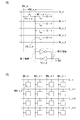
図5あるいは図6に使用できるセンスアンプ回路SAおよび選択トランジスタSTrの回路レイアウトの例を図7(A)乃至図7(F)に示す。図7(A)乃至図7(C)は、図6のフォールデッドビット線型DRAMの回路に用いることのできるセンスアンプの配線等のレイアウトを、図7(D)乃至図7(F)は、図5のオープンビット線型の回路に用いることのできるセンスアンプの配線等のレイアウトを示す。詳細は公知の半導体集積回路技術を参照できる。 Examples of circuit layouts of the sense amplifier circuit SA and the selection transistor STr that can be used in FIG. 5 or FIG. 6 are shown in FIGS. 7A to 7C show layouts of the wiring and the like of the sense amplifier that can be used in the folded bit line type DRAM circuit of FIG. 6, and FIGS. 6 shows a layout of a sense amplifier wiring and the like that can be used in the open bit line type circuit of FIG. For details, known semiconductor integrated circuit technology can be referred to.
図7(A)は半導体基板等に形成される素子形成領域とその上に設けられる第1配線等の例を示している。すなわち、素子形成領域302nと素子形成領域302pを設け、その上に重ねて第1配線301a乃至301cを形成する。これらはいずれもトランジスタのゲートとして機能する。例えば、第1配線301aは選択線SLとして機能する。また、第1配線301bおよび301cはセンスアンプ回路SA内のインバータのゲートとなる。
FIG. 7A shows an example of an element formation region formed on a semiconductor substrate or the like and a first wiring or the like provided thereon. That is, the
第1配線301a乃至301cを用いて自己整合的にn型あるいはp型の不純物をドーピングできる。ここでは、素子形成領域302nにn型トランジスタを、素子形成領域302pにp型トランジスタを形成する。さらに、素子形成領域302nと素子形成領域302pには図に示すように上層への接続に用いる第1コンタクトプラグを設ける。
The
図7(B)は、図7(A)に示した回路の上に形成される第2配線303a、303b、303n、303pと上層への第2コンタクトプラグのレイアウトを示す。第2配線303aおよび303bはn型トランジスタのドレインとp型トランジスタのドレインを接続するために設けられ、第2配線303nおよび303pは、それぞれ、n型トランジスタおよびp型トランジスタのソースに接続して、センスアンプに電源を供給するために用いられる。
FIG. 7B shows the layout of the
さらに、第1配線301bと上層、第1配線301cと上層、第2配線303aと上層、および第2配線303bと上層等への接続のために第2コンタクトプラグが設けられる。
Further, a second contact plug is provided for connection to the
図7(C)は、図7(B)に示した回路の上に形成される第3配線304a、304bと上層への第3コンタクトプラグのレイアウトを示す。第3配線304a、304bはサブビット線である。また、第3コンタクトプラグ305aおよび305bはさらに上層に設けられるビット線に接続するためのものである。上層では、ビット線はサブビット線と平行に設けられるとよいが、45°未満の角度を有してもよい。
FIG. 7C shows a layout of the
なお、第3配線304aは図の上方に形成されるインバータのゲートと下方に形成されるインバータの出力を接続し、第3配線304bは図の下方に形成されるインバータのゲートと上方に形成されるインバータの出力を接続する。
The
図7(D)は半導体基板等に形成される素子形成領域とその上に設けられる第1配線等の例を示している。すなわち、素子形成領域352nと素子形成領域352pを設け、その上に重ねて第1配線351a乃至351dを形成する。第1配線351aは例えば、選択線SL_nとして、また、第1配線351bは次の行の選択線SL_n+1として機能する。
FIG. 7D shows an example of an element formation region formed on a semiconductor substrate or the like and a first wiring or the like provided thereon. That is, the element formation region 352n and the
ここでは、素子形成領域352nにn型トランジスタを、素子形成領域352pにp型トランジスタを形成する。さらに、素子形成領域352nと素子形成領域352pには図に示すように上層への接続に用いる第1コンタクトプラグを設ける。
Here, an n-type transistor is formed in the element formation region 352n, and a p-type transistor is formed in the
図7(E)は、図7(D)に示した回路の上に形成される第2配線353a、353b、353n、353pと上層への第2コンタクトプラグのレイアウトを示す。第2配線353aおよび353bはn型トランジスタのドレインとp型トランジスタのドレインを接続するために設けられ、第2配線353nおよび353pは、それぞれ、n型トランジスタおよびp型トランジスタのソースに接続して、センスアンプに電源を供給するために用いられる。
FIG. 7E shows a layout of the
さらに、第1配線351cと上層、第1配線351dと上層、第2配線353aと上層、および第2配線353bと上層等への接続のために第2コンタクトプラグが設けられる。
Further, a second contact plug is provided for connection to the
図7(F)は、図7(E)に示した回路の上に形成される第3配線354a、354bと上層への第3コンタクトプラグのレイアウトを示す。第3配線354a、354bはサブビット線である。また、第3コンタクトプラグ355aおよび355bはさらに上層に設けられるビット線に接続するためのものである。
FIG. 7F shows a layout of the
なお、第3配線354aは図の上方に形成されるインバータのゲートと下方に形成されるインバータの出力を接続し、第3配線354bは図の下方に形成されるインバータのゲートと上方に形成されるインバータの出力を接続する。
The
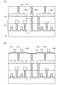
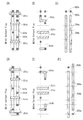
本実施の形態の半導体メモリ装置では、メモリセルは上記したセンスアンプ等の回路の上に形成される。その作製工程を図1(A)、図1(B)、図2および図3を用いて説明する。図1(A)、図1(B)、図2および図3は半導体メモリ装置のサブビット線に平行な一断面を示す。 In the semiconductor memory device of this embodiment, the memory cell is formed on a circuit such as the above-described sense amplifier. The manufacturing process will be described with reference to FIGS. 1A, 1B, 2, and 3. FIG. FIG. 1A, FIG. 1B, FIG. 2 and FIG. 3 show one cross section parallel to the sub bit line of the semiconductor memory device.
<図1(A)>
基板101上に、上記のようにトランジスタを含む半導体回路102を形成する。そして、適切な厚さの第1絶縁体103と第1コンタクトプラグ104を形成する。基板101には、表面に単結晶半導体を有するもの(例えば、単結晶半導体基板やSOI基板)を用いることが好ましい。単結晶半導体としては、単結晶シリコン、単結晶ゲルマニウム、単結晶シリコンゲルマニウム、単結晶ガリウム砒素、単結晶インジウム燐、単結晶インジウム砒素等を用いることができる。
<Fig. 1 (A)>
A
そして、第1コンタクトプラグに接するようにサブビット線105a、105c、接続電極105bを形成する。さらに、その上に適切な厚さの第2絶縁体106とサブビット線105a、105c、接続電極105bに接続する第2コンタクトプラグ107を形成する。第1絶縁体103と第2絶縁体106の厚さは、サブビット線の寄生容量を決定する上で重要である。100nm乃至1μmとすることが好ましい。また、第1絶縁体103と第2絶縁体106は酸化シリコン等の比較的誘電率の低い材料で形成するとよい。
Then, the
<図1(B)>
島状の半導体領域108a、108bを形成し、これを覆ってゲート絶縁体109を形成する。半導体領域108a、108bおよびゲート絶縁体109の厚さは適宜、決定できるが、トランジスタのチャネル長が短い場合には、いずれも薄くすることが好ましく、例えば、チャネル長の1/50乃至1/5とするとよい。なお、ゲート絶縁体109の厚さはトンネル電流等が問題とならない程度に薄くするとよい。また、ゲート絶縁体109は比誘電率が10以上の材料で形成してもよい。
<Fig. 1 (B)>
Island-shaped
半導体領域108a、108bに用いる半導体の種類には制約は無いが、移動度が5cm2/Vs以上であることが好ましい。例えば、多結晶シリコン、多結晶ゲルマニウム、多結晶シリコンゲルマニウム、インジウム酸化物あるいはインジウム酸化物に他の金属元素を添加した酸化物、窒化ガリウムあるいは窒化ガリウムに酸素を添加した化合物、砒化ガリウム、砒化インジウム、硫化亜鉛等を用いればよい。
There is no restriction on the type of semiconductor used for the
半導体領域108a、108bはセルトランジスタを構成するものであるが半導体の電界効果移動度は、さほど問題とならず、メモリセルのセルトランジスタのオン抵抗とキャパシタの容量との積が1nsec以下となるように材料を選定し、チャネル長、チャネル幅を決定すればよい。例えば、キャパシタの容量を1fFとするのであれば、オン抵抗は1MΩ以下であればよい。
Although the
本実施の形態の半導体メモリ装置では、オン抵抗よりも、むしろ、オフ抵抗の方が重要である。セルトランジスタのオフ抵抗はメモリセルのキャパシタの容量との比較で決定される。リフレッシュ周期が従来のDRAMと同程度であり、メモリセルのキャパシタの容量が従来のDRAMの1/10であれば、オフ抵抗は従来のDRAMのセルトランジスタの10倍必要である。 In the semiconductor memory device of the present embodiment, the off resistance is more important than the on resistance. The off resistance of the cell transistor is determined by comparison with the capacitance of the capacitor of the memory cell. If the refresh cycle is about the same as that of a conventional DRAM and the capacitance of the capacitor of the memory cell is 1/10 of that of the conventional DRAM, the off-resistance is 10 times that of the cell transistor of the conventional DRAM.
さらにセルトランジスタのオフ抵抗を上昇させるとメモリセルのリフレッシュ周期をより長くできるので好ましい。例えば、従来のセルトランジスタの100万倍のオフ抵抗であれば、実用的にはリフレッシュ動作を必要としないで使用できる。 Further, it is preferable to increase the off resistance of the cell transistor because the refresh cycle of the memory cell can be increased. For example, if the off resistance is 1 million times that of a conventional cell transistor, it can be used practically without requiring a refresh operation.
このような非常に高いオフ抵抗を得るためには、バンドギャップが2.5電子ボルト以上4電子ボルト以下、好ましくは3電子ボルト以上3.8電子ボルト以下のワイドバンドギャップ半導体を使用することが好ましい。例えば、酸化インジウム、酸化亜鉛等の酸化物半導体、窒化ガリウム等の窒化物半導体、硫化亜鉛等の硫化物半導体等を用いればよい。 In order to obtain such an extremely high off-resistance, it is necessary to use a wide band gap semiconductor having a band gap of 2.5 to 4 eV, preferably 3 to 3.8 eV. preferable. For example, an oxide semiconductor such as indium oxide or zinc oxide, a nitride semiconductor such as gallium nitride, a sulfide semiconductor such as zinc sulfide may be used.
オフ抵抗は、熱的に励起するキャリアの濃度に反比例する。ドナーやアクセプタによるキャリアが全く存在しない状態(真性半導体)であっても、シリコンの場合にはバンドギャップが1.1電子ボルトなので、室温(300K)での熱励起キャリアの濃度は1×1011cm−3程度である。 Off-resistance is inversely proportional to the concentration of thermally excited carriers. Even in the case where there is no carrier due to donors or acceptors (intrinsic semiconductor), in the case of silicon, the band gap is 1.1 eV, so the concentration of thermally excited carriers at room temperature (300 K) is 1 × 10 11. It is about cm −3 .
一方、バンドギャップ3.2電子ボルトの半導体では熱励起キャリアの濃度は1×10⁻⁷cm−3程度となる。電子移動度が同じ場合、抵抗率は、キャリア濃度に反比例するので、バンドギャップ3.2電子ボルトの半導体の抵抗率は、シリコンより18桁も大きい。 On the other hand, in a semiconductor with a band gap of 3.2 eV, the concentration of thermally excited carriers is about 1 × 10 −7 cm −3 . If the electron mobility is the same, the resistivity is inversely proportional to the carrier concentration, so the resistivity of a semiconductor with a band gap of 3.2 eV is 18 orders of magnitude greater than that of silicon.
なお、ドナーやアクセプタによるキャリアは極力、低濃度であることが好ましく、その濃度は、1×1012cm−3以下とすることが好ましい。これらのキャリア濃度によりトランジスタのしきい値が決定される。 In addition, it is preferable that the carrier by a donor and an acceptor is as low as possible, and it is preferable that the density | concentration shall be 1 * 10 < 12 > cm < -3 > or less. The threshold value of the transistor is determined by these carrier concentrations.
なお、シリコンを用いても、セルトランジスタのオフ抵抗を従来の100倍程度とすることは可能である。シリコンを用いるトランジスタでは、ソースドレイン間の抵抗はpn接合によって決定される。pn接合は、双方の不純物濃度が高くなると空乏層が薄くなり、トンネル電流が生じるため絶縁性が悪化する。したがって、少なくともチャネルが形成される部分のドナーあるいはアクセプタの濃度は1×1014cm−3以下とすることが好ましい。 Even if silicon is used, the off resistance of the cell transistor can be about 100 times that of the conventional one. In a transistor using silicon, the resistance between the source and the drain is determined by a pn junction. In the pn junction, when both impurity concentrations are high, the depletion layer is thinned and a tunnel current is generated, so that the insulating property is deteriorated. Therefore, it is preferable that the concentration of the donor or acceptor at least in the portion where the channel is formed is 1 × 10 14 cm −3 or less.
しかしながら、チャネルが形成される部分がそのような低濃度では、ソースからキャリアが侵入することにより絶縁性が悪化する。このことに対しては、半導体領域108a、108bを厚さ5nm以下、好ましくは1nm以下に薄膜化することで対応できる。あるいは、チャネルを縦方向に形成し、実質的なチャネル長を長くしてもよい。これらのことは、酸化物半導体等のワイドバンドギャップ半導体を用いる場合にも適用できる。
However, if the portion where the channel is formed is at such a low concentration, the insulating properties deteriorate due to the penetration of carriers from the source. This can be dealt with by reducing the thickness of the
加えて、後に形成するワード線が半導体領域にゲート絶縁体109を介して向かい合う面に、仕事関数が5電子ボルト以上の材料(例えば、白金、パラジウム等の白金族元素や窒化インジウム、窒化亜鉛等の窒化物、あるいはp型シリコン等)を用いるとよい。
In addition, a material having a work function of 5 electron volts or more (for example, a platinum group element such as platinum or palladium, indium nitride, zinc nitride, or the like) is formed on a surface where a word line to be formed later faces the semiconductor region through the
半導体領域108a、108bとゲート絶縁体109を形成した後、ワード線110a乃至110dを形成する。ワード線110a乃至110dはメモリセルのセルトランジスタのゲートとしても機能する。
After the
なお、一般に、下層に半導体集積回路が設けられている場合には、それらによって発生するノイズが上層のトランジスタの動作に支障をもたらすことがある。この問題に対しては、上層のトランジスタの下、特にサブビット線105a、105cの下に何らかのシールド層を設けて、ノイズを吸収させるとよい。
In general, when a semiconductor integrated circuit is provided in the lower layer, noise generated by the semiconductor integrated circuit may interfere with the operation of the upper transistor. In order to solve this problem, it is preferable to provide some shield layer under the upper-layer transistor, particularly under the
<図2>
イオン注入法等により、半導体領域108a、108bにワード線110a乃至110dをマスクとして不純物を注入し、n型あるいはp型のドーピングされた領域111を形成する。なお、第2コンタクトプラグ107が半導体領域108a、108bと接する部分とワード線110a乃至110dとの距離、あるいは、後で形成する第3コンタクトプラグと半導体領域108a、108bと接する部分と110a乃至110dとの距離が20nm以下、好ましくは10nm以下の場合には、ドーピングされた領域111を形成しなくてもよい。
<Figure 2>
Impurities are implanted into the
また、半導体領域108a、108bが予め何らかの導電型を有している場合には、ワード線110a乃至110dを構成する材料との仕事関数差を利用して、トランジスタの制御をおこなえるので、特にドーピングされた領域111を形成することが不要となることもある。
In addition, when the
例えば、酸化シリコン上の多結晶シリコンは特別に不純物をドーピングしなくとも、n型を呈するが、ワード線110a乃至110dに窒化インジウム、窒化亜鉛、p型シリコン等の仕事関数が5電子ボルト以上の材料を用いると、電子を排除することにより、極めて抵抗率の高い領域を形成することができる。
For example, polycrystalline silicon on silicon oxide exhibits n-type without special impurity doping, but the work function of indium nitride, zinc nitride, p-type silicon or the like for
次に、酸化シリコン等の比較的誘電率の低い材料で第3絶縁体112を形成して、第3コンタクトプラグ113を形成する。さらに、誘電率の低い材料で第4絶縁体114を形成し、これにキャパシタを形成するための孔を設ける。なお、本実施の形態では、メモリセルのキャパシタの容量を従来のDRAMの1/10以下とできるので、孔の深さも従来のDRAMの1/10以下、すなわち、0.3μm以下、好ましくは30nm以下とできる。
Next, the
このように孔を浅く形成できることは、その後に形成するキャパシタの電極や絶縁体を孔の内面に形成する上で有利である。すなわち、アスペクト比が50倍を超えるような深い孔の内面にこれらを形成するには技術的に大きな困難が伴い、歩留まりの低下をもたらす。また、より誘電率の高い絶縁体や導電率の高い電極材料はそのような条件では形成できないこともある、これに対し、例えば、アスペクト比が10倍以下であれば、比較的容易に、電極や絶縁体を形成でき、また、より多くの好ましい材料を使用することができる。 The ability to form the hole in such a shallow manner is advantageous in forming the capacitor electrode and insulator to be formed later on the inner surface of the hole. That is, it is technically difficult to form these on the inner surface of a deep hole having an aspect ratio exceeding 50 times, resulting in a decrease in yield. In addition, an insulator having a higher dielectric constant or an electrode material having a higher conductivity may not be formed under such conditions. On the other hand, for example, if the aspect ratio is 10 times or less, the electrode can be formed relatively easily. And insulators can be formed, and more preferred materials can be used.
そして、孔の内面に厚さ2nm乃至20nmの第1キャパシタ電極115a乃至115dを形成する。なお、第1キャパシタ電極115a乃至115dの厚さの上限は最小加工寸法Fに応じて、決定すればよく、Fが20nmであれば、5nm以下とすることが好ましく、Fが10nmであれば、2.5nm以下とすることが好ましい。
Then,
さらに、第4コンタクトプラグ116を形成する。
Further, a
<図3>
厚さ2nm乃至20nmのキャパシタ絶縁体117を形成する。キャパシタ絶縁体117としては各種のhigh−k材料を用いることができるが、酸化ハフニウム、酸化ジルコニウム、酸化タンタル、チタン酸バリウムストロンチウム等が好ましい。
<Figure 3>
A
さらに、第2キャパシタ電極118a、118bを形成する。その後、第5絶縁体119、第5コンタクトプラグ120を形成し、第5コンタクトプラグ120と接するようにビット線121を形成する。
Further,
(実施の形態2)
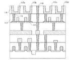
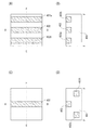
図8(A)乃至図8(D)および図9(A)乃至図9(D)に本実施の形態を示す。なお、本実施の形態でも、実施の形態1と同様にセンスアンプ等の半導体回路上にメモリセルが形成されるが、図8(A)乃至図8(D)、図9(A)乃至図9(D)では、そのような半導体回路は省略する。以下、図面にしたがって説明する。
(Embodiment 2)
8A to 8D and FIGS. 9A to 9D show this embodiment mode. Note that in this embodiment mode as well, memory cells are formed over a semiconductor circuit such as a sense amplifier in the same manner as in
<図8(A)>
第1絶縁体401の上にサブビット線402を形成する。このとき、サブビット線402の配置にはいくつかの方式がある。例えば、図9(A)と図9(B)に示すように、サブビット線402と隣接するサブビット線402a、402bを全て同じ深さあるいは同じ層に形成する方法である。図9(A)はサブビット線402を形成した面を図8(A)の線分CDを含む平面で切断した断面の模式図であり、図9(A)の線分EFの断面を図9(B)に示す。なお、図9(A)および図9(C)の線分ABの断面は図8に示される。
<FIG. 8 (A)>
A
図9(B)に示されるように、サブビット線402に隣接するサブビット線402a、402bとも同じ深さ、あるいは同じ層に形成される。この方法は作製工程が少ないという特徴がある。
As shown in FIG. 9B, the
もうひとつの方法は、図9(C)と図9(D)に示すように、サブビット線402と隣接するサブビット線402a、402bを、異なる深さあるいは異なる層に形成する方法である。図9(C)は図8(A)の線分CDを含む平面で切断した断面の模式図であり、図9(C)の線分EFの断面を図9(D)に示す。
The other method is a method in which the
図9(C)では、隣接するサブビット線402a、402bが見えないが、図9(D)に示されるように、隣接するサブビット線402a、402bはサブビット線402とは異なる深さに形成されている。この方法では追加の作製工程が必要であるが、同じ層にサブビット線を形成する方法より隣接するサブビット線間の寄生容量を低減できる。図9(D)では、サブビット線の深さは2種類としたが、3種類以上とすることもできる。
In FIG. 9C, the adjacent
従来のDRAMではサブビット線が配置される部分にはキャパシタ等の構造物があり、サブビット線の配置はきわめて制限されていたが、本実施の形態では、キャパシタはサブビット線から離れた場所に形成されるため、サブビット線の配置の自由度が高く、上記のような深さの異なるサブビット線を形成することもできる。本実施の形態ではいずれの方法も採用することができる。 In the conventional DRAM, there is a structure such as a capacitor in the portion where the sub bit line is arranged, and the arrangement of the sub bit line is extremely limited. However, in this embodiment, the capacitor is formed at a location away from the sub bit line. Therefore, the degree of freedom of arrangement of the sub bit lines is high, and sub bit lines having different depths as described above can be formed. Any method can be employed in the present embodiment.
上述のように、本発明の一様態においては、メモリセルのキャパシタの容量を低減する上では、ビット線の寄生容量を低減するよりもサブビット線の寄生容量を低減することの方が効果的である。このような方法でサブビット線の寄生容量を低減することによって、キャパシタを小さく形成できれば、工定数の増加に見合う効果が得られる。 As described above, in one embodiment of the present invention, it is more effective to reduce the parasitic capacitance of the sub-bit line than to reduce the parasitic capacitance of the bit line in reducing the capacitance of the memory cell capacitor. is there. If the capacitor can be made small by reducing the parasitic capacitance of the sub-bit line by such a method, an effect commensurate with the increase in the work constant can be obtained.
次に、第2絶縁体403および第3絶縁体404を形成する。第2絶縁体403および第3絶縁体404は異種の材料あるいはエッチングレートの異なる材料とするとよい。例えば、第2絶縁体403として酸化シリコン、第3絶縁体404として、窒化シリコンを用いることができる。そして、第2絶縁体403および第3絶縁体404にサブビット線402に接続する第1コンタクトプラグ405を埋め込む。
Next, the
次に、絶縁体および導電層を形成し、これを溝状にエッチングして、溝408およびこれにより分断される第4絶縁体406、導電層407a、407bを形成する。この際、エッチングは第3絶縁体で停止するようにする。すなわち、第3絶縁体がエッチングストッパーとなる。
Next, an insulator and a conductive layer are formed and etched into a groove shape, whereby a
<図8(B)>
次に、溝408の底面および側面に半導体膜を形成し、半導体膜および導電層407a、407bをエッチングして、島状の半導体領域409を形成する。さらにゲート絶縁体410を半導体領域409上に形成する。
<FIG. 8 (B)>
Next, a semiconductor film is formed on the bottom and side surfaces of the
<図8(C)>
その後、導電性材料の膜を形成し、これを異方性エッチングすることにより、溝408の側面のゲート絶縁体410に接するワード線411a、411bを形成する。溝の側面にこのようなワード線411a、411bを形成する方法は、特許文献1を参照すればよい。また、特許文献1に開示されているように、ワード線411a、411bをマスクとして不純物を半導体領域409にドーピングしてもよい。
<FIG. 8 (C)>
Thereafter, a film of a conductive material is formed and anisotropically etched to form
このように形成されるワード線411a、411bを用いたトランジスタでは、チャネル長を最小加工寸法より大きくすることができる。すなわち、チャネル長はおおよそ、溝408の深さとワード線411a(あるいはワード線411b)の水平方向の長さ(図8(C)中にxで示す)との和である。溝408の深さを最小加工寸法より大きくすると、チャネル長は最小加工寸法より大きくなり、短チャネル効果を抑制できる。
In the transistor using the
また、長さxは最小加工寸法とは無関係に設定できる。例えば、必要な導電性さえ確保できれば、長さxを最小加工寸法の1/2以下、好ましくは1/4以下とできる。すると、溝408の幅は最小加工線幅の2倍以下、好ましくは1倍とできる。その結果、1つのメモリセルの面積を5F2、好ましくは4F2とできる。
The length x can be set regardless of the minimum processing dimension. For example, as long as necessary conductivity can be ensured, the length x can be set to 1/2 or less, preferably 1/4 or less of the minimum processing dimension. Then, the width of the
例えば、溝408の幅を2Fとしたとき、長さxは、好ましくは0.7F以下であれば、同じ溝408に形成されるワード線411aと411bが分離できる。この結果、1つのメモリセルが必要な長さは2.5Fであり、1つのメモリセルの面積は、線分ABに垂直な方向(すなわち、図9の線分EF方向)の長さ(サブビット線間隔)2Fとの積である5F2とできる。
For example, when the width of the
また、溝408の幅をFとしたとき、長さxは、好ましくは0.3F以下であれば、同じ溝408に形成されるワード線411aと411bが分離できる。この結果、1つのメモリセルが必要な長さは2Fであり、1つのメモリセルの面積は4F2とできる。これはマトリクス型のメモリセルアレイでの理論上の下限値である。
When the width of the
なお、このような高密度化、小面積化はサブビット線402が半導体領域409の下にあるために可能であり、サブビット線がワード線の上にあると、溝408の側面にワード線を形成する方法であっても、より大きな面積が必要である。これは、溝408にワード線に加えて、サブビット線とのコンタクトを設ける必要があるためである。コンタクトがワード線と接触してはならないことから、溝408の幅はFより大きく、現実には2Fより大きくすることが必須となる。
Such high density and small area are possible because the
<図8(D)>
第5絶縁体412を形成し、さらに、導電層407a、407bと接続する第2コンタクトプラグ413a、413bを形成する。導電層407a、407bはエッチングストッパーとしての機能を有し、特に半導体領域409が薄い場合には効果的である。第2コンタクトプラグ413a、413b上には実施の形態1で示したようにキャパシタを形成し、さらに、その上にはビット線を形成すればよい。
<FIG. 8 (D)>
A
101 基板
102 半導体回路
103 第1絶縁体
104 第1コンタクトプラグ
105a サブビット線
105b 接続電極
105c サブビット線
106 第2絶縁体
107 第2コンタクトプラグ
108a 半導体領域
108b 半導体領域
109 ゲート絶縁体
110a ワード線
110b ワード線
110c ワード線
110d ワード線
111 ドーピングされた領域
112 第3絶縁体
113 第3コンタクトプラグ
114 第4絶縁体
115a 第1キャパシタ電極
115b 第1キャパシタ電極
115c 第1キャパシタ電極
115d 第1キャパシタ電極
116 第4コンタクトプラグ
117 キャパシタ絶縁体
118a 第2キャパシタ電極
118b 第2キャパシタ電極
119 第5絶縁体
120 第5コンタクトプラグ
121 ビット線
301a 第1配線
301b 第1配線
301c 第1配線
302n 素子形成領域
302p 素子形成領域
303a 第2配線
303b 第2配線
303n 第2配線
303p 第2配線
304a 第3配線
304b 第3配線
305a 第3コンタクトプラグ
305b 第3コンタクトプラグ
351a 第1配線
351b 第1配線
351c 第1配線
351d 第1配線
352n 素子形成領域
352p 素子形成領域
353a 第2配線
353b 第2配線
353n 第2配線
353p 第2配線
354a 第3配線
354b 第3配線
355a 第3コンタクトプラグ
355b 第3コンタクトプラグ
401 第1絶縁体
402 サブビット線
402a サブビット線
402b サブビット線
403 第2絶縁体
404 第3絶縁体
405 第1コンタクトプラグ
406 第4絶縁体
407a 導電層
407b 導電層
408 溝
409 半導体領域
410 ゲート絶縁体
411a ワード線
411b ワード線
412 第5絶縁体
413a 第2コンタクトプラグ
413b 第2コンタクトプラグ
MC メモリセル
MBK メモリブロック
MBL ビット線
SA センスアンプ回路
SBL サブビット線
SL 選択線
STr 選択トランジスタ
V_REF 参照電位
WL ワード線
101 Substrate 102 Semiconductor Circuit 103 First Insulator 104 First Contact Plug 105a Sub Bit Line 105b Connection Electrode 105c Sub Bit Line 106 Second Insulator 107 Second Contact Plug 108a Semiconductor Region 108b Semiconductor Region 109 Gate Insulator 110a Word Line 110b Word Line 110c word line 110d word line 111 doped region 112 third insulator 113 third contact plug 114 fourth insulator 115a first capacitor electrode 115b first capacitor electrode 115c first capacitor electrode 115d first capacitor electrode 116 fourth contact Plug 117 Capacitor insulator 118a Second capacitor electrode 118b Second capacitor electrode 119 Fifth insulator 120 Fifth contact plug 121 Bit line 301a First wiring 01b First wiring 301c First wiring 302n Element formation region 302p Element formation region 303a Second wiring 303b Second wiring 303n Second wiring 303p Second wiring 304a Third wiring 304b Third wiring 305a Third contact plug 305b Third contact plug 351a First wiring 351b First wiring 351c First wiring 351d First wiring 352n Element formation region 352p Element formation region 353a Second wiring 353b Second wiring 353n Second wiring 353p Second wiring 354a Third wiring 354b Third wiring 355a First 3rd contact plug 355b 3rd contact plug 401 1st insulator 402 Sub bit line 402a Sub bit line 402b Sub bit line 403 2nd insulator 404 3rd insulator 405 1st contact plug 406 4th insulator 407a Conductive layer 4 7b Conductive layer 408 Groove 409 Semiconductor region 410 Gate insulator 411a Word line 411b Word line 412 Fifth insulator 413a Second contact plug 413b Second contact plug MC Memory cell MBK Memory block MBL Bit line SA Sense amplifier circuit SBL Sub bit line SL Select line STr Select transistor V_REF Reference potential WL Word line
Claims (6)
前記半導体回路上の、1以上のビット線と4以上のワード線と2以上のメモリブロックと、を有し、
前記半導体回路は、1以上のセンスアンプ回路を有し、
前記メモリブロックは、2以上のメモリセルと、サブビット線とを有し、
前記メモリセルは、1以上のセルトランジスタと、1以上のキャパシタとを有し、
前記セルトランジスタは、前記サブビット線の上にあり、
前記キャパシタは、前記セルトランジスタの上にあり、
前記ビット線は、前記キャパシタの上にあり、
前記セルトランジスタは、半導体層と前記ワード線の一とで構成され、
前記ワード線の一は、前記セルトランジスタのゲート電極として機能し、
前記半導体層のバンドギャップは、3電子ボルト以上3.8電子ボルト以下であり、
前記ビット線は、前記半導体回路と電気的に接続され、
前記センスアンプ回路の第1の端子は第1のメモリブロックのサブビット線に接続され、
前記センスアンプ回路の第2の端子は第2のメモリブロックのサブビット線に接続され、
前記第1のメモリブロックのサブビット線は、該メモリブロックの半導体層と接続され、
前記第2のメモリブロックのサブビット線は、該メモリブロックの半導体層と接続されていることを特徴とする半導体メモリ装置。 A semiconductor circuit provided on a substrate;
Wherein on the semiconductor circuit, having one or more bit lines and 4 or more word lines and two or more memory blocks, and
The semiconductor circuit has one or more sense amplifier circuits,
The memory block includes two or more memory cells and a sub bit line.
The memory cell has a one or more of the cell transistor, and one or more capacitors,
The cell transistor is on the sub-bit line;
The capacitor is on the cell transistor;
The bit line is on the capacitor;
The cell transistor includes a semiconductor layer and one of the word lines,
One of the word lines functions as a gate electrode of the cell transistor,
The band gap of the semiconductor layer is not less than 3 electron volts and not more than 3.8 electron volts,
The bit line is electrically connected to the semiconductor circuit;
A first terminal of the sense amplifier circuit is connected to a sub-bit line of the first memory block;
A second terminal of the sense amplifier circuit is connected to a sub-bit line of a second memory block;
A sub bit line of the first memory block is connected to a semiconductor layer of the memory block;
A semiconductor memory device , wherein the sub-bit line of the second memory block is connected to a semiconductor layer of the memory block .
前記第1のメモリブロックのサブビット線は、前記第2のメモリブロックのサブビット線と異なる層に形成されていることを特徴とする半導体メモリ装置。 In claim 1,
The sub-bit line of the first memory block, a semi-conductor memory device you characterized in that it is formed in a layer different from the sub-bit line of said second memory block.
前記メモリブロックが有するメモリセルは、64以下であることを特徴とする半導体メモリ装置。 In claim 1 or claim 2,
Memory cells wherein the memory block has the semi-conductor memory device you wherein a is 64 or less.
前記半導体回路は、前記センスアンプ回路を駆動するための回路を有することを特徴とする半導体メモリ装置。 In any one of Claim 1 thru | or 3,
The semiconductor circuit, semi-conductor memory device you further comprising a circuit for driving the sense amplifier circuit.
前記半導体層は、凹部あるいは凸部の側面に形成された部分を有することを特徴とする半導体メモリ装置。 In any one of Claims 1 thru | or 4,
2. The semiconductor memory device according to claim 1 , wherein the semiconductor layer includes a portion formed on a side surface of the concave portion or the convex portion.
前記キャパシタの容量は、0.1fF以上1fF以下であることを特徴とする半導体メモリ装置。 In any one of Claims 1 thru | or 5,
Capacitance of the capacitor, the semi-conductor memory device you characterized in that at least 0.1FF 1 fF or less.
Priority Applications (1)
| Application Number | Priority Date | Filing Date | Title |
|---|---|---|---|
| JP2012019406A JP6000560B2 (en) | 2011-02-02 | 2012-02-01 | Semiconductor memory device |
Applications Claiming Priority (3)
| Application Number | Priority Date | Filing Date | Title |
|---|---|---|---|
| JP2011020732 | 2011-02-02 | ||
| JP2011020732 | 2011-02-02 | ||
| JP2012019406A JP6000560B2 (en) | 2011-02-02 | 2012-02-01 | Semiconductor memory device |
Publications (2)
| Publication Number | Publication Date |
|---|---|
| JP2012178554A JP2012178554A (en) | 2012-09-13 |
| JP6000560B2 true JP6000560B2 (en) | 2016-09-28 |
Family
ID=46577237
Family Applications (1)
| Application Number | Title | Priority Date | Filing Date |
|---|---|---|---|
| JP2012019406A Active JP6000560B2 (en) | 2011-02-02 | 2012-02-01 | Semiconductor memory device |
Country Status (2)
| Country | Link |
|---|---|
| US (1) | US8780614B2 (en) |
| JP (1) | JP6000560B2 (en) |
Families Citing this family (21)
| Publication number | Priority date | Publication date | Assignee | Title |
|---|---|---|---|---|
| TWI574259B (en) | 2010-09-29 | 2017-03-11 | 半導體能源研究所股份有限公司 | Semiconductor memory device and driving method thereof |
| TWI539456B (en) * | 2010-10-05 | 2016-06-21 | 半導體能源研究所股份有限公司 | Semiconductor memory device and driving method thereof |
| US8975680B2 (en) | 2011-02-17 | 2015-03-10 | Semiconductor Energy Laboratory Co., Ltd. | Semiconductor memory device and method manufacturing semiconductor memory device |
| JP5901927B2 (en) * | 2011-10-06 | 2016-04-13 | 株式会社半導体エネルギー研究所 | Semiconductor device |
| US9105351B2 (en) | 2011-11-09 | 2015-08-11 | Semiconductor Energy Laboratory Co., Ltd. | Semiconductor memory device including amplifier circuit |
| JP6100559B2 (en) | 2012-03-05 | 2017-03-22 | 株式会社半導体エネルギー研究所 | Semiconductor memory device |
| US9647125B2 (en) * | 2013-05-20 | 2017-05-09 | Semiconductor Energy Laboratory Co., Ltd. | Semiconductor device and method for manufacturing the same |
| US9607991B2 (en) | 2013-09-05 | 2017-03-28 | Semiconductor Energy Laboratory Co., Ltd. | Semiconductor device |
| TWI735206B (en) * | 2014-04-10 | 2021-08-01 | 日商半導體能源研究所股份有限公司 | Memory device and semiconductor device |
| JP6635670B2 (en) | 2014-04-11 | 2020-01-29 | 株式会社半導体エネルギー研究所 | Semiconductor device |
| WO2015170220A1 (en) | 2014-05-09 | 2015-11-12 | Semiconductor Energy Laboratory Co., Ltd. | Memory device and electronic device |
| KR102513517B1 (en) * | 2015-07-30 | 2023-03-22 | 가부시키가이샤 한도오따이 에네루기 켄큐쇼 | Semiconductor device and electronic device |
| US9564217B1 (en) | 2015-10-19 | 2017-02-07 | United Microelectronics Corp. | Semiconductor memory device having integrated DOSRAM and NOSRAM |
| US9749567B2 (en) | 2015-11-29 | 2017-08-29 | United Microelectronics Corp. | Operating method of image sensor |
| JP6917700B2 (en) * | 2015-12-02 | 2021-08-11 | 株式会社半導体エネルギー研究所 | Semiconductor device |
| US9704874B2 (en) * | 2015-12-09 | 2017-07-11 | Easic Corporation | ROM segmented bitline circuit |
| US10032492B2 (en) | 2016-03-18 | 2018-07-24 | Semiconductor Energy Laboratory Co., Ltd. | Semiconductor device, driver IC, computer and electronic device |
| US9991266B2 (en) | 2016-06-13 | 2018-06-05 | United Microelectronics Corp. | Semiconductor memory device and semiconductor memory array comprising the same |
| US10541375B2 (en) | 2016-07-21 | 2020-01-21 | Semiconductor Energy Laboratory Co., Ltd. | Display device and electronic device |
| JP7784381B2 (en) * | 2020-09-22 | 2025-12-11 | 株式会社半導体エネルギー研究所 | Semiconductor device and electronic device |
| US20230389283A1 (en) * | 2022-05-31 | 2023-11-30 | Taiwan Semiconductor Manufacturing Company Ltd. | Memory device with back-gate transistor and method of forming the same |
Family Cites Families (135)
| Publication number | Priority date | Publication date | Assignee | Title |
|---|---|---|---|---|
| JPS60124963A (en) * | 1983-12-12 | 1985-07-04 | Semiconductor Energy Lab Co Ltd | Insulated gate semiconductor device |
| JPS6363197A (en) | 1986-09-03 | 1988-03-19 | Toshiba Corp | Semiconductor storage device |
| JP2618938B2 (en) * | 1987-11-25 | 1997-06-11 | 株式会社東芝 | Semiconductor storage device |
| JP2547615B2 (en) | 1988-06-16 | 1996-10-23 | 三菱電機株式会社 | Read-only semiconductor memory device and semiconductor memory device |
| US5144583A (en) * | 1989-01-09 | 1992-09-01 | Kabushiki Kaisha Toshiba | Dynamic semiconductor memory device with twisted bit-line structure |
| US5302843A (en) | 1990-07-26 | 1994-04-12 | Semiconductor Energy Laboratory Co., Ltd. | Improved vertical channel transistor |
| JP3128829B2 (en) * | 1990-12-26 | 2001-01-29 | ソニー株式会社 | Semiconductor memory device |
| KR100307602B1 (en) * | 1993-08-30 | 2001-12-15 | 가나이 쓰도무 | Semiconductor integrated circuit device and manufacturing method thereof |
| JPH0878635A (en) * | 1994-08-31 | 1996-03-22 | Toshiba Corp | Semiconductor memory device |
| DE69635107D1 (en) | 1995-08-03 | 2005-09-29 | Koninkl Philips Electronics Nv | SEMICONDUCTOR ARRANGEMENT WITH A TRANSPARENT CIRCUIT ELEMENT |
| JP3625598B2 (en) | 1995-12-30 | 2005-03-02 | 三星電子株式会社 | Manufacturing method of liquid crystal display device |
| TW326553B (en) | 1996-01-22 | 1998-02-11 | Handotai Energy Kenkyusho Kk | Semiconductor device and method of fabricating same |
| US7052941B2 (en) * | 2003-06-24 | 2006-05-30 | Sang-Yun Lee | Method for making a three-dimensional integrated circuit structure |
| JP3266850B2 (en) * | 1997-03-27 | 2002-03-18 | 松下電器産業株式会社 | Semiconductor memory |
| KR100259078B1 (en) * | 1997-08-14 | 2000-06-15 | 김영환 | Thin film transistor and its manufacturing method |
| JP4170454B2 (en) | 1998-07-24 | 2008-10-22 | Hoya株式会社 | Article having transparent conductive oxide thin film and method for producing the same |
| JP2000150861A (en) | 1998-11-16 | 2000-05-30 | Tdk Corp | Oxide thin film |
| JP3276930B2 (en) | 1998-11-17 | 2002-04-22 | 科学技術振興事業団 | Transistor and semiconductor device |
| TW460731B (en) | 1999-09-03 | 2001-10-21 | Ind Tech Res Inst | Electrode structure and production method of wide viewing angle LCD |
| TW587252B (en) * | 2000-01-18 | 2004-05-11 | Hitachi Ltd | Semiconductor memory device and data processing device |
| JP4089858B2 (en) | 2000-09-01 | 2008-05-28 | 国立大学法人東北大学 | Semiconductor device |
| KR20020038482A (en) | 2000-11-15 | 2002-05-23 | 모리시타 요이찌 | Thin film transistor array, method for producing the same, and display panel using the same |
| JP3997731B2 (en) | 2001-03-19 | 2007-10-24 | 富士ゼロックス株式会社 | Method for forming a crystalline semiconductor thin film on a substrate |
| JP2002289859A (en) | 2001-03-23 | 2002-10-04 | Minolta Co Ltd | Thin film transistor |
| US6574148B2 (en) | 2001-07-12 | 2003-06-03 | Micron Technology, Inc. | Dual bit line driver for memory |
| JP4090716B2 (en) | 2001-09-10 | 2008-05-28 | 雅司 川崎 | Thin film transistor and matrix display device |
| JP3925839B2 (en) | 2001-09-10 | 2007-06-06 | シャープ株式会社 | Semiconductor memory device and test method thereof |
| JP4164562B2 (en) | 2002-09-11 | 2008-10-15 | 独立行政法人科学技術振興機構 | Transparent thin film field effect transistor using homologous thin film as active layer |
| WO2003040441A1 (en) | 2001-11-05 | 2003-05-15 | Japan Science And Technology Agency | Natural superlattice homologous single crystal thin film, method for preparation thereof, and device using said single crystal thin film |
| JP4083486B2 (en) | 2002-02-21 | 2008-04-30 | 独立行政法人科学技術振興機構 | Method for producing LnCuO (S, Se, Te) single crystal thin film |
| US7049190B2 (en) | 2002-03-15 | 2006-05-23 | Sanyo Electric Co., Ltd. | Method for forming ZnO film, method for forming ZnO semiconductor layer, method for fabricating semiconductor device, and semiconductor device |
| JP3933591B2 (en) | 2002-03-26 | 2007-06-20 | 淳二 城戸 | Organic electroluminescent device |
| US7339187B2 (en) | 2002-05-21 | 2008-03-04 | State Of Oregon Acting By And Through The Oregon State Board Of Higher Education On Behalf Of Oregon State University | Transistor structures |
| JP2004022625A (en) | 2002-06-13 | 2004-01-22 | Murata Mfg Co Ltd | Semiconductor device and method of manufacturing the semiconductor device |
| US7105868B2 (en) | 2002-06-24 | 2006-09-12 | Cermet, Inc. | High-electron mobility transistor with zinc oxide |
| JP2004119457A (en) * | 2002-09-24 | 2004-04-15 | Matsushita Electric Ind Co Ltd | Semiconductor storage device |
| US7067843B2 (en) | 2002-10-11 | 2006-06-27 | E. I. Du Pont De Nemours And Company | Transparent oxide semiconductor thin film transistors |
| JP2004200598A (en) * | 2002-12-20 | 2004-07-15 | Renesas Technology Corp | Semiconductor storage and semiconductor device |
| JP4166105B2 (en) | 2003-03-06 | 2008-10-15 | シャープ株式会社 | Semiconductor device and manufacturing method thereof |
| JP2004273732A (en) | 2003-03-07 | 2004-09-30 | Sharp Corp | Active matrix substrate and manufacturing method thereof |
| US6839258B2 (en) | 2003-05-12 | 2005-01-04 | Micron Technology, Inc. | Folded DRAM CAM cell |
| JP4108633B2 (en) | 2003-06-20 | 2008-06-25 | シャープ株式会社 | THIN FILM TRANSISTOR, MANUFACTURING METHOD THEREOF, AND ELECTRONIC DEVICE |
| US7262463B2 (en) | 2003-07-25 | 2007-08-28 | Hewlett-Packard Development Company, L.P. | Transistor including a deposited channel region having a doped portion |
| US7145174B2 (en) | 2004-03-12 | 2006-12-05 | Hewlett-Packard Development Company, Lp. | Semiconductor device |
| US7282782B2 (en) | 2004-03-12 | 2007-10-16 | Hewlett-Packard Development Company, L.P. | Combined binary oxide semiconductor device |
| EP1737044B1 (en) | 2004-03-12 | 2014-12-10 | Japan Science and Technology Agency | Amorphous oxide and thin film transistor |
| US7297977B2 (en) | 2004-03-12 | 2007-11-20 | Hewlett-Packard Development Company, L.P. | Semiconductor device |
| KR100555564B1 (en) * | 2004-03-31 | 2006-03-03 | 삼성전자주식회사 | Semiconductor element employing square storage electrode and its manufacturing method |
| US7211825B2 (en) | 2004-06-14 | 2007-05-01 | Yi-Chi Shih | Indium oxide-based thin film transistors and circuits |
| JP2006100760A (en) | 2004-09-02 | 2006-04-13 | Casio Comput Co Ltd | Thin film transistor and manufacturing method thereof |
| US7285501B2 (en) | 2004-09-17 | 2007-10-23 | Hewlett-Packard Development Company, L.P. | Method of forming a solution processed device |
| US7298084B2 (en) | 2004-11-02 | 2007-11-20 | 3M Innovative Properties Company | Methods and displays utilizing integrated zinc oxide row and column drivers in conjunction with organic light emitting diodes |
| WO2006051995A1 (en) | 2004-11-10 | 2006-05-18 | Canon Kabushiki Kaisha | Field effect transistor employing an amorphous oxide |
| US7453065B2 (en) | 2004-11-10 | 2008-11-18 | Canon Kabushiki Kaisha | Sensor and image pickup device |
| US7863611B2 (en) | 2004-11-10 | 2011-01-04 | Canon Kabushiki Kaisha | Integrated circuits utilizing amorphous oxides |
| RU2358354C2 (en) | 2004-11-10 | 2009-06-10 | Кэнон Кабусики Кайся | Light-emitting device |
| US7791072B2 (en) | 2004-11-10 | 2010-09-07 | Canon Kabushiki Kaisha | Display |
| CN102945857B (en) | 2004-11-10 | 2015-06-03 | 佳能株式会社 | Amorphous oxide and field effect transistor |
| US7829444B2 (en) | 2004-11-10 | 2010-11-09 | Canon Kabushiki Kaisha | Field effect transistor manufacturing method |
| US7579224B2 (en) | 2005-01-21 | 2009-08-25 | Semiconductor Energy Laboratory Co., Ltd. | Method for manufacturing a thin film semiconductor device |
| TWI505473B (en) | 2005-01-28 | 2015-10-21 | 半導體能源研究所股份有限公司 | Semiconductor device, electronic device, and method of manufacturing semiconductor device |
| TWI569441B (en) | 2005-01-28 | 2017-02-01 | 半導體能源研究所股份有限公司 | Semiconductor device, electronic device, and method of manufacturing semiconductor device |
| US7858451B2 (en) | 2005-02-03 | 2010-12-28 | Semiconductor Energy Laboratory Co., Ltd. | Electronic device, semiconductor device and manufacturing method thereof |
| US7948171B2 (en) | 2005-02-18 | 2011-05-24 | Semiconductor Energy Laboratory Co., Ltd. | Light emitting device |
| US20060197092A1 (en) | 2005-03-03 | 2006-09-07 | Randy Hoffman | System and method for forming conductive material on a substrate |
| US8681077B2 (en) | 2005-03-18 | 2014-03-25 | Semiconductor Energy Laboratory Co., Ltd. | Semiconductor device, and display device, driving method and electronic apparatus thereof |
| US7544967B2 (en) | 2005-03-28 | 2009-06-09 | Massachusetts Institute Of Technology | Low voltage flexible organic/transparent transistor for selective gas sensing, photodetecting and CMOS device applications |
| US7645478B2 (en) | 2005-03-31 | 2010-01-12 | 3M Innovative Properties Company | Methods of making displays |
| US8300031B2 (en) | 2005-04-20 | 2012-10-30 | Semiconductor Energy Laboratory Co., Ltd. | Semiconductor device comprising transistor having gate and drain connected through a current-voltage conversion element |
| JP2006344849A (en) | 2005-06-10 | 2006-12-21 | Casio Comput Co Ltd | Thin film transistor |
| US7402506B2 (en) | 2005-06-16 | 2008-07-22 | Eastman Kodak Company | Methods of making thin film transistors comprising zinc-oxide-based semiconductor materials and transistors made thereby |
| US7691666B2 (en) | 2005-06-16 | 2010-04-06 | Eastman Kodak Company | Methods of making thin film transistors comprising zinc-oxide-based semiconductor materials and transistors made thereby |
| US7499307B2 (en) * | 2005-06-24 | 2009-03-03 | Mosys, Inc. | Scalable embedded DRAM array |
| US7507618B2 (en) | 2005-06-27 | 2009-03-24 | 3M Innovative Properties Company | Method for making electronic devices using metal oxide nanoparticles |
| KR100711890B1 (en) | 2005-07-28 | 2007-04-25 | 삼성에스디아이 주식회사 | OLED display and manufacturing method thereof |
| JP2007042172A (en) | 2005-08-01 | 2007-02-15 | Sony Corp | Semiconductor memory device |
| JP2007059128A (en) | 2005-08-23 | 2007-03-08 | Canon Inc | Organic EL display device and manufacturing method thereof |
| JP4280736B2 (en) | 2005-09-06 | 2009-06-17 | キヤノン株式会社 | Semiconductor element |
| JP2007073705A (en) | 2005-09-06 | 2007-03-22 | Canon Inc | Oxide semiconductor channel thin film transistor and method for manufacturing the same |
| JP4850457B2 (en) | 2005-09-06 | 2012-01-11 | キヤノン株式会社 | Thin film transistor and thin film diode |
| JP5116225B2 (en) | 2005-09-06 | 2013-01-09 | キヤノン株式会社 | Manufacturing method of oxide semiconductor device |
| JP5078246B2 (en) | 2005-09-29 | 2012-11-21 | 株式会社半導体エネルギー研究所 | Semiconductor device and manufacturing method of semiconductor device |
| EP1995787A3 (en) | 2005-09-29 | 2012-01-18 | Semiconductor Energy Laboratory Co, Ltd. | Semiconductor device having oxide semiconductor layer and manufacturing method therof |
| JP5064747B2 (en) | 2005-09-29 | 2012-10-31 | 株式会社半導体エネルギー研究所 | Semiconductor device, electrophoretic display device, display module, electronic device, and method for manufacturing semiconductor device |
| JP5037808B2 (en) | 2005-10-20 | 2012-10-03 | キヤノン株式会社 | Field effect transistor using amorphous oxide, and display device using the transistor |
| KR101050767B1 (en) | 2005-11-15 | 2011-07-20 | 가부시키가이샤 한도오따이 에네루기 켄큐쇼 | Method of Manufacturing a Semiconductor Device |
| JP2007179602A (en) * | 2005-12-27 | 2007-07-12 | Hitachi Ltd | Semiconductor device |
| TWI292281B (en) | 2005-12-29 | 2008-01-01 | Ind Tech Res Inst | Pixel structure of active organic light emitting diode and method of fabricating the same |
| US7867636B2 (en) | 2006-01-11 | 2011-01-11 | Murata Manufacturing Co., Ltd. | Transparent conductive film and method for manufacturing the same |
| JP4977478B2 (en) | 2006-01-21 | 2012-07-18 | 三星電子株式会社 | ZnO film and method of manufacturing TFT using the same |
| US7982252B2 (en) * | 2006-01-27 | 2011-07-19 | Hynix Semiconductor Inc. | Dual-gate non-volatile ferroelectric memory |
| US7576394B2 (en) | 2006-02-02 | 2009-08-18 | Kochi Industrial Promotion Center | Thin film transistor including low resistance conductive thin films and manufacturing method thereof |
| US7977169B2 (en) | 2006-02-15 | 2011-07-12 | Kochi Industrial Promotion Center | Semiconductor device including active layer made of zinc oxide with controlled orientations and manufacturing method thereof |
| KR20070101595A (en) | 2006-04-11 | 2007-10-17 | 삼성전자주식회사 | ZnO TFT |
| US20070252928A1 (en) | 2006-04-28 | 2007-11-01 | Toppan Printing Co., Ltd. | Structure, transmission type liquid crystal display, reflection type display and manufacturing method thereof |
| JP5028033B2 (en) | 2006-06-13 | 2012-09-19 | キヤノン株式会社 | Oxide semiconductor film dry etching method |
| CN101595530B (en) * | 2006-07-27 | 2012-12-05 | 意法半导体有限公司 | Circuit for reading a charge retention element for temporal measurement |
| JP4609797B2 (en) | 2006-08-09 | 2011-01-12 | Nec液晶テクノロジー株式会社 | Thin film device and manufacturing method thereof |
| JP4999400B2 (en) | 2006-08-09 | 2012-08-15 | キヤノン株式会社 | Oxide semiconductor film dry etching method |
| JP4332545B2 (en) | 2006-09-15 | 2009-09-16 | キヤノン株式会社 | Field effect transistor and manufacturing method thereof |
| JP4274219B2 (en) | 2006-09-27 | 2009-06-03 | セイコーエプソン株式会社 | Electronic devices, organic electroluminescence devices, organic thin film semiconductor devices |
| JP5164357B2 (en) | 2006-09-27 | 2013-03-21 | キヤノン株式会社 | Semiconductor device and manufacturing method of semiconductor device |
| US7622371B2 (en) | 2006-10-10 | 2009-11-24 | Hewlett-Packard Development Company, L.P. | Fused nanocrystal thin film semiconductor and method |
| US7376027B1 (en) * | 2006-11-07 | 2008-05-20 | Taiwan Semiconductor Manufacturing Co., Ltd. | DRAM concurrent writing and sensing scheme |
| US7772021B2 (en) | 2006-11-29 | 2010-08-10 | Samsung Electronics Co., Ltd. | Flat panel displays comprising a thin-film transistor having a semiconductive oxide in its channel and methods of fabricating the same for use in flat panel displays |
| JP2008140684A (en) | 2006-12-04 | 2008-06-19 | Toppan Printing Co Ltd | Color EL display and manufacturing method thereof |
| KR101303578B1 (en) | 2007-01-05 | 2013-09-09 | 삼성전자주식회사 | Etching method of thin film |
| US8207063B2 (en) | 2007-01-26 | 2012-06-26 | Eastman Kodak Company | Process for atomic layer deposition |
| KR100851215B1 (en) | 2007-03-14 | 2008-08-07 | 삼성에스디아이 주식회사 | Thin film transistor and organic light emitting display device using same |
| US7795613B2 (en) | 2007-04-17 | 2010-09-14 | Toppan Printing Co., Ltd. | Structure with transistor |
| KR101325053B1 (en) | 2007-04-18 | 2013-11-05 | 삼성디스플레이 주식회사 | Thin film transistor substrate and manufacturing method thereof |
| KR20080094300A (en) | 2007-04-19 | 2008-10-23 | 삼성전자주식회사 | Thin film transistors and methods of manufacturing the same and flat panel displays comprising thin film transistors |
| KR101334181B1 (en) | 2007-04-20 | 2013-11-28 | 삼성전자주식회사 | Thin Film Transistor having selectively crystallized channel layer and method of manufacturing the same |
| US8274078B2 (en) | 2007-04-25 | 2012-09-25 | Canon Kabushiki Kaisha | Metal oxynitride semiconductor containing zinc |
| US20080266925A1 (en) | 2007-04-30 | 2008-10-30 | International Business Machines Corporation | Array Split Across Three-Dimensional Interconnected Chips |
| US7719905B2 (en) * | 2007-05-17 | 2010-05-18 | Hynix Semiconductor, Inc. | Semiconductor memory device |
| KR101345376B1 (en) | 2007-05-29 | 2013-12-24 | 삼성전자주식회사 | Fabrication method of ZnO family Thin film transistor |
| JP5430846B2 (en) * | 2007-12-03 | 2014-03-05 | 株式会社半導体エネルギー研究所 | Method for manufacturing semiconductor device |
| JP5215158B2 (en) | 2007-12-17 | 2013-06-19 | 富士フイルム株式会社 | Inorganic crystalline alignment film, method for manufacturing the same, and semiconductor device |
| US7746680B2 (en) | 2007-12-27 | 2010-06-29 | Sandisk 3D, Llc | Three dimensional hexagonal matrix memory array |
| US7715246B1 (en) * | 2008-06-27 | 2010-05-11 | Juhan Kim | Mask ROM with light bit line architecture |
| JP4623179B2 (en) | 2008-09-18 | 2011-02-02 | ソニー株式会社 | Thin film transistor and manufacturing method thereof |
| JP5451280B2 (en) | 2008-10-09 | 2014-03-26 | キヤノン株式会社 | Wurtzite crystal growth substrate, manufacturing method thereof, and semiconductor device |
| CN104485336B (en) | 2009-10-21 | 2018-01-02 | 株式会社半导体能源研究所 | Semiconductor device with a plurality of transistors |
| EP2494597A4 (en) | 2009-10-30 | 2015-03-18 | Semiconductor Energy Lab | SEMICONDUCTOR DEVICE |
| WO2011062029A1 (en) | 2009-11-18 | 2011-05-26 | Semiconductor Energy Laboratory Co., Ltd. | Memory device |
| WO2012029638A1 (en) | 2010-09-03 | 2012-03-08 | Semiconductor Energy Laboratory Co., Ltd. | Semiconductor device |
| JP2012256821A (en) | 2010-09-13 | 2012-12-27 | Semiconductor Energy Lab Co Ltd | Memory device |
| TWI539453B (en) | 2010-09-14 | 2016-06-21 | 半導體能源研究所股份有限公司 | Memory device and semiconductor device |
| TWI574259B (en) | 2010-09-29 | 2017-03-11 | 半導體能源研究所股份有限公司 | Semiconductor memory device and driving method thereof |
| TWI539456B (en) | 2010-10-05 | 2016-06-21 | 半導體能源研究所股份有限公司 | Semiconductor memory device and driving method thereof |
| KR102130257B1 (en) | 2010-11-05 | 2020-07-03 | 가부시키가이샤 한도오따이 에네루기 켄큐쇼 | Semiconductor device |
| TWI619230B (en) | 2011-01-14 | 2018-03-21 | 半導體能源研究所股份有限公司 | Semiconductor memory device |
| TWI520273B (en) | 2011-02-02 | 2016-02-01 | 半導體能源研究所股份有限公司 | Semiconductor storage device |
| US9431400B2 (en) * | 2011-02-08 | 2016-08-30 | Semiconductor Energy Laboratory Co., Ltd. | Semiconductor memory device and method for manufacturing the same |
-
2012
- 2012-02-01 US US13/363,584 patent/US8780614B2/en active Active
- 2012-02-01 JP JP2012019406A patent/JP6000560B2/en active Active
Also Published As
| Publication number | Publication date |
|---|---|
| JP2012178554A (en) | 2012-09-13 |
| US20120195104A1 (en) | 2012-08-02 |
| US8780614B2 (en) | 2014-07-15 |
Similar Documents
| Publication | Publication Date | Title |
|---|---|---|
| JP6000560B2 (en) | Semiconductor memory device | |
| US12176024B2 (en) | Memory device comprising an electrically floating body transistor | |
| US11348922B2 (en) | Memory cell comprising first and second transistors and methods of operating | |
| JP6224183B2 (en) | Semiconductor memory device | |
| US11974425B2 (en) | Memory cell comprising first and second transistors and methods of operating | |
| JP5651524B2 (en) | Semiconductor memory device | |
| US9472263B2 (en) | Semiconductor memory device | |
| JP6081704B2 (en) | Semiconductor memory device | |
| JP5864058B2 (en) | Semiconductor device | |
| US20080017904A1 (en) | Semiconductor device | |
| JP2016184452A (en) | Semiconductor device | |
| KR101804666B1 (en) | Semiconductor memory device with vertical semiconductor column | |
| US20240243492A1 (en) | Memory Cell Comprising First and Second Transistors and Methods of Operating |
Legal Events
| Date | Code | Title | Description |
|---|---|---|---|
| A621 | Written request for application examination |
Free format text: JAPANESE INTERMEDIATE CODE: A621 Effective date: 20150130 |
|
| A977 | Report on retrieval |
Free format text: JAPANESE INTERMEDIATE CODE: A971007 Effective date: 20151030 |
|
| A131 | Notification of reasons for refusal |
Free format text: JAPANESE INTERMEDIATE CODE: A131 Effective date: 20151104 |
|
| A521 | Request for written amendment filed |
Free format text: JAPANESE INTERMEDIATE CODE: A523 Effective date: 20151109 |
|
| A131 | Notification of reasons for refusal |
Free format text: JAPANESE INTERMEDIATE CODE: A131 Effective date: 20160405 |
|
| A521 | Request for written amendment filed |
Free format text: JAPANESE INTERMEDIATE CODE: A523 Effective date: 20160531 |
|
| TRDD | Decision of grant or rejection written | ||
| A01 | Written decision to grant a patent or to grant a registration (utility model) |
Free format text: JAPANESE INTERMEDIATE CODE: A01 Effective date: 20160802 |
|
| A61 | First payment of annual fees (during grant procedure) |
Free format text: JAPANESE INTERMEDIATE CODE: A61 Effective date: 20160831 |
|
| R150 | Certificate of patent or registration of utility model |
Ref document number: 6000560 Country of ref document: JP Free format text: JAPANESE INTERMEDIATE CODE: R150 |
|
| R250 | Receipt of annual fees |
Free format text: JAPANESE INTERMEDIATE CODE: R250 |
|
| R250 | Receipt of annual fees |
Free format text: JAPANESE INTERMEDIATE CODE: R250 |
|
| R250 | Receipt of annual fees |
Free format text: JAPANESE INTERMEDIATE CODE: R250 |
|
| R250 | Receipt of annual fees |
Free format text: JAPANESE INTERMEDIATE CODE: R250 |
|
| R250 | Receipt of annual fees |
Free format text: JAPANESE INTERMEDIATE CODE: R250 |
|
| R250 | Receipt of annual fees |
Free format text: JAPANESE INTERMEDIATE CODE: R250 |