JP5893351B2 - プリント回路板 - Google Patents
プリント回路板 Download PDFInfo
- Publication number
- JP5893351B2 JP5893351B2 JP2011246716A JP2011246716A JP5893351B2 JP 5893351 B2 JP5893351 B2 JP 5893351B2 JP 2011246716 A JP2011246716 A JP 2011246716A JP 2011246716 A JP2011246716 A JP 2011246716A JP 5893351 B2 JP5893351 B2 JP 5893351B2
- Authority
- JP
- Japan
- Prior art keywords
- semiconductor package
- wiring board
- printed wiring
- region
- solder ball
- Prior art date
- Legal status (The legal status is an assumption and is not a legal conclusion. Google has not performed a legal analysis and makes no representation as to the accuracy of the status listed.)
- Expired - Fee Related
Links
Images


Classifications
-
- H—ELECTRICITY
- H05—ELECTRIC TECHNIQUES NOT OTHERWISE PROVIDED FOR
- H05K—PRINTED CIRCUITS; CASINGS OR CONSTRUCTIONAL DETAILS OF ELECTRIC APPARATUS; MANUFACTURE OF ASSEMBLAGES OF ELECTRICAL COMPONENTS
- H05K1/00—Printed circuits
- H05K1/02—Details
- H05K1/0271—Arrangements for reducing stress or warp in rigid printed circuit boards, e.g. caused by loads, vibrations or differences in thermal expansion
-
- H—ELECTRICITY
- H05—ELECTRIC TECHNIQUES NOT OTHERWISE PROVIDED FOR
- H05K—PRINTED CIRCUITS; CASINGS OR CONSTRUCTIONAL DETAILS OF ELECTRIC APPARATUS; MANUFACTURE OF ASSEMBLAGES OF ELECTRICAL COMPONENTS
- H05K1/00—Printed circuits
- H05K1/18—Printed circuits structurally associated with non-printed electric components
- H05K1/181—Printed circuits structurally associated with non-printed electric components associated with surface mounted components
-
- H—ELECTRICITY
- H05—ELECTRIC TECHNIQUES NOT OTHERWISE PROVIDED FOR
- H05K—PRINTED CIRCUITS; CASINGS OR CONSTRUCTIONAL DETAILS OF ELECTRIC APPARATUS; MANUFACTURE OF ASSEMBLAGES OF ELECTRICAL COMPONENTS
- H05K2201/00—Indexing scheme relating to printed circuits covered by H05K1/00
- H05K2201/06—Thermal details
- H05K2201/068—Thermal details wherein the coefficient of thermal expansion is important
-
- H—ELECTRICITY
- H05—ELECTRIC TECHNIQUES NOT OTHERWISE PROVIDED FOR
- H05K—PRINTED CIRCUITS; CASINGS OR CONSTRUCTIONAL DETAILS OF ELECTRIC APPARATUS; MANUFACTURE OF ASSEMBLAGES OF ELECTRICAL COMPONENTS
- H05K2201/00—Indexing scheme relating to printed circuits covered by H05K1/00
- H05K2201/10—Details of components or other objects attached to or integrated in a printed circuit board
- H05K2201/10431—Details of mounted components
- H05K2201/10507—Involving several components
- H05K2201/10545—Related components mounted on both sides of the PCB
-
- H—ELECTRICITY
- H05—ELECTRIC TECHNIQUES NOT OTHERWISE PROVIDED FOR
- H05K—PRINTED CIRCUITS; CASINGS OR CONSTRUCTIONAL DETAILS OF ELECTRIC APPARATUS; MANUFACTURE OF ASSEMBLAGES OF ELECTRICAL COMPONENTS
- H05K2201/00—Indexing scheme relating to printed circuits covered by H05K1/00
- H05K2201/10—Details of components or other objects attached to or integrated in a printed circuit board
- H05K2201/10613—Details of electrical connections of non-printed components, e.g. special leads
- H05K2201/10621—Components characterised by their electrical contacts
- H05K2201/10734—Ball grid array [BGA]; Bump grid array
-
- H—ELECTRICITY
- H10—SEMICONDUCTOR DEVICES; ELECTRIC SOLID-STATE DEVICES NOT OTHERWISE PROVIDED FOR
- H10W—GENERIC PACKAGES, INTERCONNECTIONS, CONNECTORS OR OTHER CONSTRUCTIONAL DETAILS OF DEVICES COVERED BY CLASS H10
- H10W70/00—Package substrates; Interposers; Redistribution layers [RDL]
- H10W70/60—Insulating or insulated package substrates; Interposers; Redistribution layers
-
- H—ELECTRICITY
- H10—SEMICONDUCTOR DEVICES; ELECTRIC SOLID-STATE DEVICES NOT OTHERWISE PROVIDED FOR
- H10W—GENERIC PACKAGES, INTERCONNECTIONS, CONNECTORS OR OTHER CONSTRUCTIONAL DETAILS OF DEVICES COVERED BY CLASS H10
- H10W90/00—Package configurations
- H10W90/701—Package configurations characterised by the relative positions of pads or connectors relative to package parts
- H10W90/721—Package configurations characterised by the relative positions of pads or connectors relative to package parts of bump connectors
- H10W90/724—Package configurations characterised by the relative positions of pads or connectors relative to package parts of bump connectors between a chip and a stacked insulating package substrate, interposer or RDL
-
- Y—GENERAL TAGGING OF NEW TECHNOLOGICAL DEVELOPMENTS; GENERAL TAGGING OF CROSS-SECTIONAL TECHNOLOGIES SPANNING OVER SEVERAL SECTIONS OF THE IPC; TECHNICAL SUBJECTS COVERED BY FORMER USPC CROSS-REFERENCE ART COLLECTIONS [XRACs] AND DIGESTS
- Y02—TECHNOLOGIES OR APPLICATIONS FOR MITIGATION OR ADAPTATION AGAINST CLIMATE CHANGE
- Y02P—CLIMATE CHANGE MITIGATION TECHNOLOGIES IN THE PRODUCTION OR PROCESSING OF GOODS
- Y02P70/00—Climate change mitigation technologies in the production process for final industrial or consumer products
- Y02P70/50—Manufacturing or production processes characterised by the final manufactured product
Landscapes
- Engineering & Computer Science (AREA)
- Microelectronics & Electronic Packaging (AREA)
- Electric Connection Of Electric Components To Printed Circuits (AREA)
Priority Applications (3)
| Application Number | Priority Date | Filing Date | Title |
|---|---|---|---|
| JP2011246716A JP5893351B2 (ja) | 2011-11-10 | 2011-11-10 | プリント回路板 |
| EP12191363.6A EP2603063A1 (en) | 2011-11-10 | 2012-11-06 | Printed circuit board |
| US13/670,202 US20130119541A1 (en) | 2011-11-10 | 2012-11-06 | Printed circuit board |
Applications Claiming Priority (1)
| Application Number | Priority Date | Filing Date | Title |
|---|---|---|---|
| JP2011246716A JP5893351B2 (ja) | 2011-11-10 | 2011-11-10 | プリント回路板 |
Publications (3)
| Publication Number | Publication Date |
|---|---|
| JP2013105785A JP2013105785A (ja) | 2013-05-30 |
| JP2013105785A5 JP2013105785A5 (https=) | 2014-12-25 |
| JP5893351B2 true JP5893351B2 (ja) | 2016-03-23 |
Family
ID=47143690
Family Applications (1)
| Application Number | Title | Priority Date | Filing Date |
|---|---|---|---|
| JP2011246716A Expired - Fee Related JP5893351B2 (ja) | 2011-11-10 | 2011-11-10 | プリント回路板 |
Country Status (3)
| Country | Link |
|---|---|
| US (1) | US20130119541A1 (https=) |
| EP (1) | EP2603063A1 (https=) |
| JP (1) | JP5893351B2 (https=) |
Families Citing this family (3)
| Publication number | Priority date | Publication date | Assignee | Title |
|---|---|---|---|---|
| JP2014229761A (ja) * | 2013-05-23 | 2014-12-08 | 株式会社東芝 | 電子機器 |
| JP6230520B2 (ja) * | 2014-10-29 | 2017-11-15 | キヤノン株式会社 | プリント回路板及び電子機器 |
| JP6916471B2 (ja) * | 2017-01-19 | 2021-08-11 | 株式会社村田製作所 | 電子部品及び電子部品の製造方法 |
Family Cites Families (8)
| Publication number | Priority date | Publication date | Assignee | Title |
|---|---|---|---|---|
| JP2004273617A (ja) | 2003-03-06 | 2004-09-30 | Canon Inc | 半導体装置 |
| US7979721B2 (en) * | 2004-11-15 | 2011-07-12 | Microsoft Corporation | Enhanced packaging for PC security |
| JP4738996B2 (ja) * | 2004-12-13 | 2011-08-03 | キヤノン株式会社 | 半導体装置 |
| US8643163B2 (en) * | 2005-08-08 | 2014-02-04 | Stats Chippac Ltd. | Integrated circuit package-on-package stacking system and method of manufacture thereof |
| JP4719009B2 (ja) * | 2006-01-13 | 2011-07-06 | ルネサスエレクトロニクス株式会社 | 基板および半導体装置 |
| US20090039490A1 (en) * | 2007-08-08 | 2009-02-12 | Powertech Technology Inc. | Mounting assembly of semiconductor packages prevent soldering defects caused by substrate warpage |
| WO2011048862A1 (ja) * | 2009-10-23 | 2011-04-28 | 株式会社フジクラ | デバイス実装構造およびデバイス実装方法 |
| KR101665556B1 (ko) * | 2009-11-19 | 2016-10-13 | 삼성전자 주식회사 | 멀티 피치 볼 랜드를 갖는 반도체 패키지 |
-
2011
- 2011-11-10 JP JP2011246716A patent/JP5893351B2/ja not_active Expired - Fee Related
-
2012
- 2012-11-06 US US13/670,202 patent/US20130119541A1/en not_active Abandoned
- 2012-11-06 EP EP12191363.6A patent/EP2603063A1/en not_active Withdrawn
Also Published As
| Publication number | Publication date |
|---|---|
| US20130119541A1 (en) | 2013-05-16 |
| EP2603063A1 (en) | 2013-06-12 |
| JP2013105785A (ja) | 2013-05-30 |
Similar Documents
| Publication | Publication Date | Title |
|---|---|---|
| JP5222509B2 (ja) | 半導体装置 | |
| US20090267217A1 (en) | Semiconductor device | |
| KR102561718B1 (ko) | 인터포저 지지 구조 메커니즘을 갖는 집적 회로 패키징 시스템 및 그 제조 방법 | |
| JP2009212315A (ja) | 半導体装置及びその製造方法 | |
| US8853842B2 (en) | Semiconductor device sealed with a resin molding | |
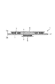
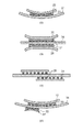
| JP5893351B2 (ja) | プリント回路板 | |
| JP6128993B2 (ja) | 積層型半導体装置、プリント回路板、電子機器及び積層型半導体装置の製造方法 | |
| JP2008277457A (ja) | 積層型半導体装置および実装体 | |
| JP4738996B2 (ja) | 半導体装置 | |
| KR101278339B1 (ko) | 코이닝 장치 | |
| JP5151878B2 (ja) | 半導体装置 | |
| JP5017881B2 (ja) | 半導体装置 | |
| US20070262437A1 (en) | Semiconductor device with temperature cycle life improved | |
| JP4878813B2 (ja) | 半導体実装装置 | |
| JP4556671B2 (ja) | 半導体パッケージ及びフレキシブルサーキット基板 | |
| JP2011159840A (ja) | 電子部品の実装接続構造 | |
| JP4976767B2 (ja) | 積層形半導体装置 | |
| JP2004047758A (ja) | 半導体装置 | |
| JP2006228932A (ja) | 半導体パッケージ | |
| JP2020072143A (ja) | 電子装置 | |
| JP2007067129A (ja) | 半導体装置の実装構造 | |
| JP2009170617A (ja) | 半導体装置 | |
| KR100924543B1 (ko) | 반도체 패키지의 제조 방법 | |
| JP2007317754A (ja) | 半導体装置 | |
| KR100772107B1 (ko) | 볼 그리드 어레이 패키지 |
Legal Events
| Date | Code | Title | Description |
|---|---|---|---|
| A521 | Request for written amendment filed |
Free format text: JAPANESE INTERMEDIATE CODE: A523 Effective date: 20141110 |
|
| A621 | Written request for application examination |
Free format text: JAPANESE INTERMEDIATE CODE: A621 Effective date: 20141110 |
|
| A977 | Report on retrieval |
Free format text: JAPANESE INTERMEDIATE CODE: A971007 Effective date: 20150622 |
|
| A131 | Notification of reasons for refusal |
Free format text: JAPANESE INTERMEDIATE CODE: A131 Effective date: 20150707 |
|
| A521 | Request for written amendment filed |
Free format text: JAPANESE INTERMEDIATE CODE: A523 Effective date: 20150907 |
|
| TRDD | Decision of grant or rejection written | ||
| A01 | Written decision to grant a patent or to grant a registration (utility model) |
Free format text: JAPANESE INTERMEDIATE CODE: A01 Effective date: 20160126 |
|
| A61 | First payment of annual fees (during grant procedure) |
Free format text: JAPANESE INTERMEDIATE CODE: A61 Effective date: 20160224 |
|
| R151 | Written notification of patent or utility model registration |
Ref document number: 5893351 Country of ref document: JP Free format text: JAPANESE INTERMEDIATE CODE: R151 |
|
| LAPS | Cancellation because of no payment of annual fees |