JP5672718B2 - 電気光学装置及び電子機器 - Google Patents
電気光学装置及び電子機器 Download PDFInfo
- Publication number
- JP5672718B2 JP5672718B2 JP2010043849A JP2010043849A JP5672718B2 JP 5672718 B2 JP5672718 B2 JP 5672718B2 JP 2010043849 A JP2010043849 A JP 2010043849A JP 2010043849 A JP2010043849 A JP 2010043849A JP 5672718 B2 JP5672718 B2 JP 5672718B2
- Authority
- JP
- Japan
- Prior art keywords
- electro
- substrate
- optical device
- support portion
- optical
- Prior art date
- Legal status (The legal status is an assumption and is not a legal conclusion. Google has not performed a legal analysis and makes no representation as to the accuracy of the status listed.)
- Active
Links
Images


Classifications
-
- G—PHYSICS
- G03—PHOTOGRAPHY; CINEMATOGRAPHY; ANALOGOUS TECHNIQUES USING WAVES OTHER THAN OPTICAL WAVES; ELECTROGRAPHY; HOLOGRAPHY
- G03B—APPARATUS OR ARRANGEMENTS FOR TAKING PHOTOGRAPHS OR FOR PROJECTING OR VIEWING THEM; APPARATUS OR ARRANGEMENTS EMPLOYING ANALOGOUS TECHNIQUES USING WAVES OTHER THAN OPTICAL WAVES; ACCESSORIES THEREFOR
- G03B33/00—Colour photography, other than mere exposure or projection of a colour film
- G03B33/10—Simultaneous recording or projection
- G03B33/12—Simultaneous recording or projection using beam-splitting or beam-combining systems, e.g. dichroic mirrors
-
- G—PHYSICS
- G02—OPTICS
- G02F—OPTICAL DEVICES OR ARRANGEMENTS FOR THE CONTROL OF LIGHT BY MODIFICATION OF THE OPTICAL PROPERTIES OF THE MEDIA OF THE ELEMENTS INVOLVED THEREIN; NON-LINEAR OPTICS; FREQUENCY-CHANGING OF LIGHT; OPTICAL LOGIC ELEMENTS; OPTICAL ANALOGUE/DIGITAL CONVERTERS
- G02F1/00—Devices or arrangements for the control of the intensity, colour, phase, polarisation or direction of light arriving from an independent light source, e.g. switching, gating or modulating; Non-linear optics
- G02F1/01—Devices or arrangements for the control of the intensity, colour, phase, polarisation or direction of light arriving from an independent light source, e.g. switching, gating or modulating; Non-linear optics for the control of the intensity, phase, polarisation or colour
- G02F1/13—Devices or arrangements for the control of the intensity, colour, phase, polarisation or direction of light arriving from an independent light source, e.g. switching, gating or modulating; Non-linear optics for the control of the intensity, phase, polarisation or colour based on liquid crystals, e.g. single liquid crystal display cells
- G02F1/133—Constructional arrangements; Operation of liquid crystal cells; Circuit arrangements
- G02F1/1333—Constructional arrangements; Manufacturing methods
- G02F1/133308—Support structures for LCD panels, e.g. frames or bezels
-
- G—PHYSICS
- G03—PHOTOGRAPHY; CINEMATOGRAPHY; ANALOGOUS TECHNIQUES USING WAVES OTHER THAN OPTICAL WAVES; ELECTROGRAPHY; HOLOGRAPHY
- G03B—APPARATUS OR ARRANGEMENTS FOR TAKING PHOTOGRAPHS OR FOR PROJECTING OR VIEWING THEM; APPARATUS OR ARRANGEMENTS EMPLOYING ANALOGOUS TECHNIQUES USING WAVES OTHER THAN OPTICAL WAVES; ACCESSORIES THEREFOR
- G03B21/00—Projectors or projection-type viewers; Accessories therefor
- G03B21/14—Details
- G03B21/145—Housing details, e.g. position adjustments thereof
-
- G—PHYSICS
- G02—OPTICS
- G02F—OPTICAL DEVICES OR ARRANGEMENTS FOR THE CONTROL OF LIGHT BY MODIFICATION OF THE OPTICAL PROPERTIES OF THE MEDIA OF THE ELEMENTS INVOLVED THEREIN; NON-LINEAR OPTICS; FREQUENCY-CHANGING OF LIGHT; OPTICAL LOGIC ELEMENTS; OPTICAL ANALOGUE/DIGITAL CONVERTERS
- G02F1/00—Devices or arrangements for the control of the intensity, colour, phase, polarisation or direction of light arriving from an independent light source, e.g. switching, gating or modulating; Non-linear optics
- G02F1/01—Devices or arrangements for the control of the intensity, colour, phase, polarisation or direction of light arriving from an independent light source, e.g. switching, gating or modulating; Non-linear optics for the control of the intensity, phase, polarisation or colour
- G02F1/13—Devices or arrangements for the control of the intensity, colour, phase, polarisation or direction of light arriving from an independent light source, e.g. switching, gating or modulating; Non-linear optics for the control of the intensity, phase, polarisation or colour based on liquid crystals, e.g. single liquid crystal display cells
- G02F1/133—Constructional arrangements; Operation of liquid crystal cells; Circuit arrangements
- G02F1/1333—Constructional arrangements; Manufacturing methods
- G02F1/133308—Support structures for LCD panels, e.g. frames or bezels
- G02F1/133311—Environmental protection, e.g. against dust or humidity
-
- G—PHYSICS
- G02—OPTICS
- G02F—OPTICAL DEVICES OR ARRANGEMENTS FOR THE CONTROL OF LIGHT BY MODIFICATION OF THE OPTICAL PROPERTIES OF THE MEDIA OF THE ELEMENTS INVOLVED THEREIN; NON-LINEAR OPTICS; FREQUENCY-CHANGING OF LIGHT; OPTICAL LOGIC ELEMENTS; OPTICAL ANALOGUE/DIGITAL CONVERTERS
- G02F1/00—Devices or arrangements for the control of the intensity, colour, phase, polarisation or direction of light arriving from an independent light source, e.g. switching, gating or modulating; Non-linear optics
- G02F1/01—Devices or arrangements for the control of the intensity, colour, phase, polarisation or direction of light arriving from an independent light source, e.g. switching, gating or modulating; Non-linear optics for the control of the intensity, phase, polarisation or colour
- G02F1/13—Devices or arrangements for the control of the intensity, colour, phase, polarisation or direction of light arriving from an independent light source, e.g. switching, gating or modulating; Non-linear optics for the control of the intensity, phase, polarisation or colour based on liquid crystals, e.g. single liquid crystal display cells
- G02F1/133—Constructional arrangements; Operation of liquid crystal cells; Circuit arrangements
- G02F1/1333—Constructional arrangements; Manufacturing methods
- G02F1/133308—Support structures for LCD panels, e.g. frames or bezels
- G02F1/133317—Intermediate frames, e.g. between backlight housing and front frame
Description
る。
<第1実施形態>
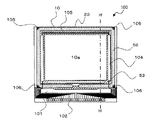
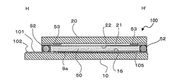
まず、本実施形態に係る電気光学装置が備える液晶パネル100の全体構成について、図1及び図2を参照して説明する。図1は、本実施形態に係る電気光学装置が備える液晶パネル100の全体構成を示す平面図である。図2は、図1のH−H´線断面図である。
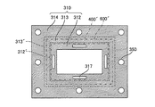
続いて、第2実施形態に係る電気光学装置について、図8を参照して説明する。図8は、本実施形態に係る電気光学装置からフレーム310を抽出して示す平面図であり、図6と同趣旨のものである。尚、本実施形態に係る電気光学装置において、上述の第1実施形態に係る電気光学装置1と共通する部位に関しては、共通の符号を付すこととし、詳細な説明は省略することとする。
続いて、第3実施形態に係る電気光学装置について、図9を参照して説明する。図9は、本実施形態に係る電気光学装置の全体構成を示す斜視図である。尚、本実施形態に係る電気光学装置において、上述の第1実施形態に係る電気光学装置1と共通する部位に関しては、共通の符号を付すこととし、詳細な説明は省略することとする。
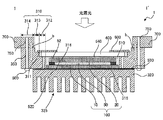
次に、上述した電気光学装置である液晶装置を各種の電子機器に適用する場合について
説明する。ここでは、本発明に係る電子機器として、投射型液晶プロジェクターを例にとる。図10は、本実施形態に係る投射型液晶プロジェクターの図式的断面図である。
Claims (13)
- 画像表示領域を有する電気光学パネルと、
前記電気光学パネルの一方の面に貼り合わされた基板と、
前記基板を支持する支持部と、前記電気光学パネルを囲むように配置される本体部とを有する保持部材と、
前記基板と前記保持部材の前記支持部との間の一部に配置された第1の接着剤と、
前記基板と前記保持部材の前記支持部との間の他の一部に配置された第2の接着剤と、
前記電気光学パネルの前記基板が貼り合わされた面とは反対側に設けられた放熱部材と、を備え、
前記画像表示領域は、対向する二辺である第1の辺及び第2の辺と、前記第1の辺及び前記第2の辺と交差した辺である第3の辺と、前記第3の辺と対向する辺である第4の辺と、を有し、
前記第1の接着剤は、前記基板の面に垂直な方向から見た平面視において、前記基板と前記支持部とが重なる部分のうち、前記第1の辺を延在した直線と前記第2の辺を延在した直線と前記第3の辺と前記基板の辺とで囲われた領域に位置し、
前記第2の接着剤は、前記基板の面に垂直な方向から見た平面視において、前記基板と前記支持部とが重なる部分のうち、前記第1の辺を延在した直線と前記第2の辺を延在した直線と前記第4の辺と前記基板の辺とで囲われた領域に位置していることを特徴とする電気光学装置。 - 前記基板の外形形状は、前記電気光学パネルの外形形状よりも大きいことを特徴とする請求項1に記載の電気光学装置。
- 前記本体部は、被実装部材側に突出するように形成された取付部を有し、
前記支持部は、前記取付部に比べて凹むように形成されていることを特徴とする請求項1又は2に記載の電気光学装置。 - 前記本体部は、前記電気光学パネルの画素領域に対応する開口部を有しており、
前記支持部は、前記開口部の縁に沿って形成されていることを特徴とする請求項3に記載の電気光学装置。 - 前記支持部は、平面的に見て、前記本体部から凸状に突出するように形成されていることを特徴とする請求項1から4のいずれか一項に記載の電気光学装置。
- 前記支持部は、前記基板の面に垂直な方向から見た平面視において、前記基板と前記支持部とが重なる部分のうち、前記第1の辺を延在した直線と前記第2の辺を延在した直線と前記第3の辺と前記基板の辺とで囲われた領域に第1の接着用開口部を有し、かつ、前記基板と前記支持部とが重なる部分のうち、前記第1の辺を延在した直線と前記第2の辺を延在した直線と前記第4の辺と前記基板の辺とで囲われた領域に第2の接着用開口部を有し、
前記第1の接着剤は、前記第1の接着用開口部に充填され、前記第2の接着剤は、前記第2の接着用開口部に充填されていることを特徴とする請求項1から5のいずれか一項に記載の電気光学装置。 - 前記基板の前記電気光学パネルに貼り合わされた面とは反対側から、前記基板及び前記本体部に接するように設けられており、平面的に見て、前記電気光学パネルの画素領域を少なくとも部分的に囲むように形成された遮光板を備えることを特徴とする請求項1から6のいずれか一項に記載の電気光学装置。
- 前記電気光学パネルは、前記放熱部材と熱伝導性を有するグリスを介して接していることを特徴とする請求項1から7のいずれか一項に記載の電気光学装置。
- 前記グリスは、前記電気光学パネルと前記放熱部材とが重なる面の一部にのみ塗布されていることを特徴とする請求項8に記載の電気光学装置。
- 前記放熱部材は、前記保持部材と一体的に形成されていることを特徴とする請求項1に記載の電気光学装置。
- 前記放熱部材の前記電気光学パネルとの対向する面とは反対側から、前記放熱部材を前記保持部材に固定するためのフック部材を備えることを特徴とする請求項1に記載の電気光学装置。
- 前記電気光学パネルは反射型であることを特徴とする請求項1から11のいずれか一項に記載の電気光学装置。
- 請求項1から12のいずれか一項に記載の電気光学装置を具備することを特徴とする電子機器。
Priority Applications (3)
| Application Number | Priority Date | Filing Date | Title |
|---|---|---|---|
| JP2010043849A JP5672718B2 (ja) | 2010-03-01 | 2010-03-01 | 電気光学装置及び電子機器 |
| US13/033,906 US9030622B2 (en) | 2010-03-01 | 2011-02-24 | Electro-optic device and electronic apparatus |
| CN201110049551.3A CN102193220B (zh) | 2010-03-01 | 2011-03-01 | 电光装置及电子设备 |
Applications Claiming Priority (1)
| Application Number | Priority Date | Filing Date | Title |
|---|---|---|---|
| JP2010043849A JP5672718B2 (ja) | 2010-03-01 | 2010-03-01 | 電気光学装置及び電子機器 |
Related Child Applications (1)
| Application Number | Title | Priority Date | Filing Date |
|---|---|---|---|
| JP2014259930A Division JP5928571B2 (ja) | 2014-12-24 | 2014-12-24 | 電気光学装置及び電子機器 |
Publications (3)
| Publication Number | Publication Date |
|---|---|
| JP2011180325A JP2011180325A (ja) | 2011-09-15 |
| JP2011180325A5 JP2011180325A5 (ja) | 2013-04-11 |
| JP5672718B2 true JP5672718B2 (ja) | 2015-02-18 |
Family
ID=44505101
Family Applications (1)
| Application Number | Title | Priority Date | Filing Date |
|---|---|---|---|
| JP2010043849A Active JP5672718B2 (ja) | 2010-03-01 | 2010-03-01 | 電気光学装置及び電子機器 |
Country Status (3)
| Country | Link |
|---|---|
| US (1) | US9030622B2 (ja) |
| JP (1) | JP5672718B2 (ja) |
| CN (1) | CN102193220B (ja) |
Families Citing this family (9)
| Publication number | Priority date | Publication date | Assignee | Title |
|---|---|---|---|---|
| TWI477882B (zh) * | 2012-05-04 | 2015-03-21 | Young Optics Inc | 投影裝置及其光閥模組 |
| JP6015620B2 (ja) * | 2013-10-16 | 2016-10-26 | トヨタ自動車株式会社 | 車両 |
| JP6351401B2 (ja) * | 2014-06-27 | 2018-07-04 | キヤノン株式会社 | 投写型表示装置および画像表示システム |
| JP2017015838A (ja) * | 2015-06-29 | 2017-01-19 | 株式会社フジクラ | 光デバイスパッケージおよび光スイッチ |
| JP2017146536A (ja) * | 2016-02-19 | 2017-08-24 | 株式会社リコー | 画像表示装置及び画像投影装置 |
| JP7106836B2 (ja) * | 2017-10-17 | 2022-07-27 | 株式会社デンソー | 表示装置 |
| JP7392372B2 (ja) | 2019-10-08 | 2023-12-06 | セイコーエプソン株式会社 | 電気光学装置および電子機器 |
| JP7392479B2 (ja) | 2020-01-14 | 2023-12-06 | 株式会社Jvcケンウッド | 表示デバイス及び投射型表示装置 |
| CN113114021B (zh) * | 2021-04-07 | 2022-05-13 | 台达电子企业管理(上海)有限公司 | 功率器件的驱动系统 |
Family Cites Families (26)
| Publication number | Priority date | Publication date | Assignee | Title |
|---|---|---|---|---|
| JPS6491114A (en) * | 1987-10-02 | 1989-04-10 | Hitachi Ltd | Liquid crystal display device |
| JPH049983A (ja) | 1990-04-27 | 1992-01-14 | Mita Ind Co Ltd | 現像トナー補給装置 |
| JPH049983U (ja) * | 1990-05-15 | 1992-01-28 | ||
| US5818564A (en) * | 1996-09-13 | 1998-10-06 | Raychem Corporation | Assembly including an active matrix liquid crystal display module |
| JPH10186333A (ja) | 1996-12-27 | 1998-07-14 | Sony Corp | 液晶表示装置 |
| JP2000193947A (ja) * | 1998-12-28 | 2000-07-14 | Canon Inc | 液晶表示装置、投射型液晶表示装置、及び液晶表示パネルの接続方法 |
| JP3697134B2 (ja) * | 1999-03-30 | 2005-09-21 | セイコーエプソン株式会社 | 電気光学装置及びこれを備えた投射型表示装置 |
| US6414781B1 (en) | 1999-03-30 | 2002-07-02 | Seiko Epson Corporation | Electro-optical device and projection display device including the same |
| JP2002296568A (ja) * | 2001-03-29 | 2002-10-09 | Victor Co Of Japan Ltd | 反射型液晶表示素子及びその製造方法 |
| JP2003279954A (ja) * | 2002-03-22 | 2003-10-02 | Sony Corp | 液晶表示装置 |
| JP4029383B2 (ja) * | 2002-06-03 | 2008-01-09 | 日本ビクター株式会社 | 反射型液晶表示素子 |
| JP2004037874A (ja) * | 2002-07-03 | 2004-02-05 | Seiko Epson Corp | 実装ケース入り電気光学装置及び投射型表示装置 |
| JP2004053964A (ja) * | 2002-07-19 | 2004-02-19 | Sony Corp | 液晶表示装置 |
| JP2004341455A (ja) * | 2003-03-14 | 2004-12-02 | Tochigi Nikon Corp | 投射型表示装置 |
| JP2004062197A (ja) * | 2003-08-28 | 2004-02-26 | Seiko Epson Corp | 実装ケース入り電気光学装置及び投射型表示装置 |
| JP4380295B2 (ja) * | 2003-10-29 | 2009-12-09 | ソニー株式会社 | 反射型液晶表示素子および画像投影装置 |
| JP2006119169A (ja) * | 2004-10-19 | 2006-05-11 | Seiko Epson Corp | 電気光学装置用実装ケース、及び電気光学装置、並びに電子機器 |
| JP2007121505A (ja) * | 2005-10-26 | 2007-05-17 | Victor Co Of Japan Ltd | 反射型液晶表示装置 |
| JP2007199153A (ja) * | 2006-01-24 | 2007-08-09 | Victor Co Of Japan Ltd | 反射型液晶表示装置 |
| JP2007206364A (ja) * | 2006-02-01 | 2007-08-16 | Victor Co Of Japan Ltd | 液晶表示素子 |
| CN101162316A (zh) * | 2006-10-13 | 2008-04-16 | 鸿富锦精密工业(深圳)有限公司 | 直下式背光模组 |
| JP2008129031A (ja) * | 2006-11-16 | 2008-06-05 | Seiko Epson Corp | 電気光学装置、及びこれを備えた電子機器 |
| JP5504557B2 (ja) * | 2007-09-21 | 2014-05-28 | セイコーエプソン株式会社 | 電気光学装置及び電気光学装置用実装ケース、並びに電子機器 |
| JP5078650B2 (ja) * | 2008-02-12 | 2012-11-21 | キヤノン株式会社 | 画像表示装置 |
| JP4900304B2 (ja) * | 2008-03-31 | 2012-03-21 | 富士通株式会社 | 携帯端末装置 |
| JP5598006B2 (ja) * | 2010-02-03 | 2014-10-01 | ソニー株式会社 | 液晶表示装置及び投射型表示装置 |
-
2010
- 2010-03-01 JP JP2010043849A patent/JP5672718B2/ja active Active
-
2011
- 2011-02-24 US US13/033,906 patent/US9030622B2/en active Active
- 2011-03-01 CN CN201110049551.3A patent/CN102193220B/zh active Active
Also Published As
| Publication number | Publication date |
|---|---|
| CN102193220A (zh) | 2011-09-21 |
| CN102193220B (zh) | 2015-07-08 |
| JP2011180325A (ja) | 2011-09-15 |
| US20110211152A1 (en) | 2011-09-01 |
| US9030622B2 (en) | 2015-05-12 |
Similar Documents
| Publication | Publication Date | Title |
|---|---|---|
| JP5533001B2 (ja) | 電気光学装置及び電子機器 | |
| JP5672718B2 (ja) | 電気光学装置及び電子機器 | |
| JP5515813B2 (ja) | 電気光学装置及び電子機器 | |
| JP5487704B2 (ja) | 電気光学装置及び電子機器 | |
| JP5504683B2 (ja) | 電気光学装置及び電子機器 | |
| JP5731122B2 (ja) | 電気光学装置及び電子機器 | |
| JP5470800B2 (ja) | 電気光学装置及び電子機器 | |
| JP2010256666A (ja) | 電気光学装置及び電子機器 | |
| JP5544749B2 (ja) | 電気光学装置及び電子機器 | |
| JP4333756B2 (ja) | 放熱部材、電気光学装置及び電子機器 | |
| JP6108004B2 (ja) | 電気光学装置及び電子機器 | |
| JP2015197650A (ja) | 電気光学装置、及び電子機器 | |
| JP5381282B2 (ja) | 電気光学装置及び電子機器 | |
| JP2010256662A (ja) | 電気光学装置及び電子機器 | |
| JP5928571B2 (ja) | 電気光学装置及び電子機器 | |
| JP5124974B2 (ja) | 電気光学装置、及びこれを備えた電子機器 | |
| JP5187268B2 (ja) | 電気光学装置及び電子機器 | |
| JP2015200687A (ja) | 電気光学装置、及び電子機器 | |
| JP5181736B2 (ja) | 電気光学装置及び電子機器 | |
| JP2010256663A (ja) | 電気光学装置及び電子機器 | |
| JP2010256667A (ja) | 電気光学装置及び電子機器 | |
| JP2010113187A (ja) | 電気光学装置及び電子機器 | |
| JP2015200688A (ja) | 電気光学装置、及び電子機器 | |
| JP2010175889A (ja) | 電気光学装置及び電子機器 | |
| JP2010175818A (ja) | 電気光学装置及び電子機器 |
Legal Events
| Date | Code | Title | Description |
|---|---|---|---|
| A521 | Written amendment |
Free format text: JAPANESE INTERMEDIATE CODE: A523 Effective date: 20130222 |
|
| A621 | Written request for application examination |
Free format text: JAPANESE INTERMEDIATE CODE: A621 Effective date: 20130222 |
|
| A977 | Report on retrieval |
Free format text: JAPANESE INTERMEDIATE CODE: A971007 Effective date: 20131114 |
|
| A131 | Notification of reasons for refusal |
Free format text: JAPANESE INTERMEDIATE CODE: A131 Effective date: 20131119 |
|
| A521 | Written amendment |
Free format text: JAPANESE INTERMEDIATE CODE: A523 Effective date: 20140117 |
|
| A131 | Notification of reasons for refusal |
Free format text: JAPANESE INTERMEDIATE CODE: A131 Effective date: 20140401 |
|
| A521 | Written amendment |
Free format text: JAPANESE INTERMEDIATE CODE: A523 Effective date: 20140529 |
|
| TRDD | Decision of grant or rejection written | ||
| A01 | Written decision to grant a patent or to grant a registration (utility model) |
Free format text: JAPANESE INTERMEDIATE CODE: A01 Effective date: 20141202 |
|
| A61 | First payment of annual fees (during grant procedure) |
Free format text: JAPANESE INTERMEDIATE CODE: A61 Effective date: 20141215 |
|
| R150 | Certificate of patent or registration of utility model |
Ref document number: 5672718 Country of ref document: JP Free format text: JAPANESE INTERMEDIATE CODE: R150 |
|
| S531 | Written request for registration of change of domicile |
Free format text: JAPANESE INTERMEDIATE CODE: R313531 |
|
| R350 | Written notification of registration of transfer |
Free format text: JAPANESE INTERMEDIATE CODE: R350 |