JP5597263B2 - 微細構造積層体、微細構造積層体の作製方法及び微細構造体の製造方法 - Google Patents
微細構造積層体、微細構造積層体の作製方法及び微細構造体の製造方法 Download PDFInfo
- Publication number
- JP5597263B2 JP5597263B2 JP2012547902A JP2012547902A JP5597263B2 JP 5597263 B2 JP5597263 B2 JP 5597263B2 JP 2012547902 A JP2012547902 A JP 2012547902A JP 2012547902 A JP2012547902 A JP 2012547902A JP 5597263 B2 JP5597263 B2 JP 5597263B2
- Authority
- JP
- Japan
- Prior art keywords
- layer
- microstructure
- sol
- inorganic
- gel material
- Prior art date
- Legal status (The legal status is an assumption and is not a legal conclusion. Google has not performed a legal analysis and makes no representation as to the accuracy of the status listed.)
- Active
Links
- 238000004519 manufacturing process Methods 0.000 title claims description 120
- 239000010410 layer Substances 0.000 claims description 846
- 229920005989 resin Polymers 0.000 claims description 554
- 239000011347 resin Substances 0.000 claims description 554
- 239000000463 material Substances 0.000 claims description 512
- 239000010408 film Substances 0.000 claims description 187
- 239000000758 substrate Substances 0.000 claims description 139
- 238000000034 method Methods 0.000 claims description 136
- NIXOWILDQLNWCW-UHFFFAOYSA-M Acrylate Chemical compound [O-]C(=O)C=C NIXOWILDQLNWCW-UHFFFAOYSA-M 0.000 claims description 131
- 229910010272 inorganic material Inorganic materials 0.000 claims description 113
- 239000011147 inorganic material Substances 0.000 claims description 113
- 238000012546 transfer Methods 0.000 claims description 109
- 239000010419 fine particle Substances 0.000 claims description 94
- 229910052731 fluorine Inorganic materials 0.000 claims description 89
- 239000011737 fluorine Substances 0.000 claims description 88
- YCKRFDGAMUMZLT-UHFFFAOYSA-N Fluorine atom Chemical compound [F] YCKRFDGAMUMZLT-UHFFFAOYSA-N 0.000 claims description 87
- 239000011521 glass Substances 0.000 claims description 76
- 230000008569 process Effects 0.000 claims description 50
- 239000013039 cover film Substances 0.000 claims description 41
- 239000000203 mixture Substances 0.000 claims description 39
- VYPSYNLAJGMNEJ-UHFFFAOYSA-N Silicium dioxide Chemical compound O=[Si]=O VYPSYNLAJGMNEJ-UHFFFAOYSA-N 0.000 claims description 37
- 229910052751 metal Inorganic materials 0.000 claims description 36
- 239000002184 metal Substances 0.000 claims description 36
- 150000004703 alkoxides Chemical class 0.000 claims description 31
- CDBYLPFSWZWCQE-UHFFFAOYSA-L Sodium Carbonate Chemical compound [Na+].[Na+].[O-]C([O-])=O CDBYLPFSWZWCQE-UHFFFAOYSA-L 0.000 claims description 30
- 238000010438 heat treatment Methods 0.000 claims description 26
- 239000003999 initiator Substances 0.000 claims description 25
- 230000002093 peripheral effect Effects 0.000 claims description 18
- 229920000642 polymer Polymers 0.000 claims description 18
- 238000003475 lamination Methods 0.000 claims description 17
- 239000012790 adhesive layer Substances 0.000 claims description 16
- 239000005357 flat glass Substances 0.000 claims description 16
- 239000011230 binding agent Substances 0.000 claims description 15
- 230000003287 optical effect Effects 0.000 claims description 12
- XUIMIQQOPSSXEZ-UHFFFAOYSA-N Silicon Chemical compound [Si] XUIMIQQOPSSXEZ-UHFFFAOYSA-N 0.000 claims description 10
- 229910052710 silicon Inorganic materials 0.000 claims description 10
- 239000010703 silicon Substances 0.000 claims description 9
- PXHVJJICTQNCMI-UHFFFAOYSA-N Nickel Chemical compound [Ni] PXHVJJICTQNCMI-UHFFFAOYSA-N 0.000 claims description 8
- 229910052782 aluminium Inorganic materials 0.000 claims description 8
- 229910052594 sapphire Inorganic materials 0.000 claims description 7
- 239000010980 sapphire Substances 0.000 claims description 7
- XAGFODPZIPBFFR-UHFFFAOYSA-N aluminium Chemical compound [Al] XAGFODPZIPBFFR-UHFFFAOYSA-N 0.000 claims description 6
- 238000005323 electroforming Methods 0.000 claims description 6
- 229910052759 nickel Inorganic materials 0.000 claims description 4
- VYZAMTAEIAYCRO-UHFFFAOYSA-N Chromium Chemical compound [Cr] VYZAMTAEIAYCRO-UHFFFAOYSA-N 0.000 claims description 3
- 229910052804 chromium Inorganic materials 0.000 claims description 3
- 239000011651 chromium Substances 0.000 claims description 3
- 239000000243 solution Substances 0.000 description 144
- -1 polyethylene terephthalate Polymers 0.000 description 138
- 238000001723 curing Methods 0.000 description 95
- LFQSCWFLJHTTHZ-UHFFFAOYSA-N Ethanol Chemical compound CCO LFQSCWFLJHTTHZ-UHFFFAOYSA-N 0.000 description 75
- 229920001296 polysiloxane Polymers 0.000 description 61
- 239000002585 base Substances 0.000 description 60
- 238000000576 coating method Methods 0.000 description 46
- OKKJLVBELUTLKV-UHFFFAOYSA-N Methanol Chemical class OC OKKJLVBELUTLKV-UHFFFAOYSA-N 0.000 description 39
- 239000011248 coating agent Substances 0.000 description 35
- 230000004048 modification Effects 0.000 description 32
- 238000012986 modification Methods 0.000 description 32
- 239000012299 nitrogen atmosphere Substances 0.000 description 32
- 239000004698 Polyethylene Substances 0.000 description 31
- 229920000573 polyethylene Polymers 0.000 description 31
- YXFVVABEGXRONW-UHFFFAOYSA-N Toluene Chemical compound CC1=CC=CC=C1 YXFVVABEGXRONW-UHFFFAOYSA-N 0.000 description 30
- 229920002799 BoPET Polymers 0.000 description 29
- 239000002904 solvent Substances 0.000 description 29
- 150000001875 compounds Chemical class 0.000 description 28
- 239000000126 substance Substances 0.000 description 25
- 238000001035 drying Methods 0.000 description 24
- KFZMGEQAYNKOFK-UHFFFAOYSA-N Isopropanol Chemical compound CC(C)O KFZMGEQAYNKOFK-UHFFFAOYSA-N 0.000 description 23
- 239000000047 product Substances 0.000 description 23
- XLYOFNOQVPJJNP-UHFFFAOYSA-N water Substances O XLYOFNOQVPJJNP-UHFFFAOYSA-N 0.000 description 23
- 238000000016 photochemical curing Methods 0.000 description 22
- 238000011282 treatment Methods 0.000 description 22
- 230000007613 environmental effect Effects 0.000 description 21
- 125000000524 functional group Chemical group 0.000 description 21
- 239000006087 Silane Coupling Agent Substances 0.000 description 19
- 230000000052 comparative effect Effects 0.000 description 18
- 230000007774 longterm Effects 0.000 description 18
- 125000000391 vinyl group Chemical group [H]C([*])=C([H])[H] 0.000 description 18
- 230000001681 protective effect Effects 0.000 description 17
- 238000002834 transmittance Methods 0.000 description 17
- 239000000853 adhesive Substances 0.000 description 16
- 230000001070 adhesive effect Effects 0.000 description 16
- ZWEHNKRNPOVVGH-UHFFFAOYSA-N 2-Butanone Chemical compound CCC(C)=O ZWEHNKRNPOVVGH-UHFFFAOYSA-N 0.000 description 15
- 238000011156 evaluation Methods 0.000 description 15
- QNODIIQQMGDSEF-UHFFFAOYSA-N (1-hydroxycyclohexyl)-phenylmethanone Chemical compound C=1C=CC=CC=1C(=O)C1(O)CCCCC1 QNODIIQQMGDSEF-UHFFFAOYSA-N 0.000 description 14
- BOTDANWDWHJENH-UHFFFAOYSA-N Tetraethyl orthosilicate Chemical compound CCO[Si](OCC)(OCC)OCC BOTDANWDWHJENH-UHFFFAOYSA-N 0.000 description 14
- 125000003647 acryloyl group Chemical group O=C([*])C([H])=C([H])[H] 0.000 description 14
- 125000003700 epoxy group Chemical group 0.000 description 14
- 239000000178 monomer Substances 0.000 description 14
- 229920000139 polyethylene terephthalate Polymers 0.000 description 13
- 239000005020 polyethylene terephthalate Substances 0.000 description 13
- 229920005992 thermoplastic resin Polymers 0.000 description 13
- 238000004804 winding Methods 0.000 description 13
- VEXZGXHMUGYJMC-UHFFFAOYSA-N Hydrochloric acid Chemical compound Cl VEXZGXHMUGYJMC-UHFFFAOYSA-N 0.000 description 12
- GWEVSGVZZGPLCZ-UHFFFAOYSA-N Titan oxide Chemical compound O=[Ti]=O GWEVSGVZZGPLCZ-UHFFFAOYSA-N 0.000 description 12
- 239000013500 performance material Substances 0.000 description 12
- YHWCPXVTRSHPNY-UHFFFAOYSA-N butan-1-olate;titanium(4+) Chemical compound [Ti+4].CCCC[O-].CCCC[O-].CCCC[O-].CCCC[O-] YHWCPXVTRSHPNY-UHFFFAOYSA-N 0.000 description 11
- 125000004432 carbon atom Chemical group C* 0.000 description 11
- ARXJGSRGQADJSQ-UHFFFAOYSA-N 1-methoxypropan-2-ol Chemical compound COCC(C)O ARXJGSRGQADJSQ-UHFFFAOYSA-N 0.000 description 10
- CVBUKMMMRLOKQR-UHFFFAOYSA-N 1-phenylbutane-1,3-dione Chemical compound CC(=O)CC(=O)C1=CC=CC=C1 CVBUKMMMRLOKQR-UHFFFAOYSA-N 0.000 description 10
- 239000012298 atmosphere Substances 0.000 description 10
- 238000006243 chemical reaction Methods 0.000 description 10
- 238000001459 lithography Methods 0.000 description 10
- 229920002545 silicone oil Polymers 0.000 description 10
- 238000012360 testing method Methods 0.000 description 10
- 239000010936 titanium Substances 0.000 description 10
- KBQVDAIIQCXKPI-UHFFFAOYSA-N 3-trimethoxysilylpropyl prop-2-enoate Chemical compound CO[Si](OC)(OC)CCCOC(=O)C=C KBQVDAIIQCXKPI-UHFFFAOYSA-N 0.000 description 9
- 239000004743 Polypropylene Substances 0.000 description 9
- DAKWPKUUDNSNPN-UHFFFAOYSA-N Trimethylolpropane triacrylate Chemical compound C=CC(=O)OCC(CC)(COC(=O)C=C)COC(=O)C=C DAKWPKUUDNSNPN-UHFFFAOYSA-N 0.000 description 9
- 230000000694 effects Effects 0.000 description 9
- 229920000728 polyester Polymers 0.000 description 9
- 229920001955 polyphenylene ether Polymers 0.000 description 9
- 229920001155 polypropylene Polymers 0.000 description 9
- 239000004065 semiconductor Substances 0.000 description 9
- LFQCEHFDDXELDD-UHFFFAOYSA-N tetramethyl orthosilicate Chemical compound CO[Si](OC)(OC)OC LFQCEHFDDXELDD-UHFFFAOYSA-N 0.000 description 9
- 125000003903 2-propenyl group Chemical group [H]C([*])([H])C([H])=C([H])[H] 0.000 description 8
- YRKCREAYFQTBPV-UHFFFAOYSA-N acetylacetone Chemical compound CC(=O)CC(C)=O YRKCREAYFQTBPV-UHFFFAOYSA-N 0.000 description 8
- 238000010586 diagram Methods 0.000 description 8
- 238000005516 engineering process Methods 0.000 description 8
- 229920002313 fluoropolymer Polymers 0.000 description 8
- 239000004811 fluoropolymer Substances 0.000 description 8
- 150000007529 inorganic bases Chemical class 0.000 description 8
- 238000010030 laminating Methods 0.000 description 8
- 239000003607 modifier Substances 0.000 description 8
- 238000006116 polymerization reaction Methods 0.000 description 8
- JOYRKODLDBILNP-UHFFFAOYSA-N Ethyl urethane Chemical compound CCOC(N)=O JOYRKODLDBILNP-UHFFFAOYSA-N 0.000 description 7
- 229920001328 Polyvinylidene chloride Polymers 0.000 description 7
- 239000002253 acid Substances 0.000 description 7
- KPUWHANPEXNPJT-UHFFFAOYSA-N disiloxane Chemical class [SiH3]O[SiH3] KPUWHANPEXNPJT-UHFFFAOYSA-N 0.000 description 7
- 238000010894 electron beam technology Methods 0.000 description 7
- LYCAIKOWRPUZTN-UHFFFAOYSA-N ethylene glycol Natural products OCCO LYCAIKOWRPUZTN-UHFFFAOYSA-N 0.000 description 7
- 230000004927 fusion Effects 0.000 description 7
- 230000001678 irradiating effect Effects 0.000 description 7
- 230000000704 physical effect Effects 0.000 description 7
- 239000004800 polyvinyl chloride Substances 0.000 description 7
- 229920000915 polyvinyl chloride Polymers 0.000 description 7
- 239000005033 polyvinylidene chloride Substances 0.000 description 7
- 238000012545 processing Methods 0.000 description 7
- 239000002994 raw material Substances 0.000 description 7
- 229910052719 titanium Inorganic materials 0.000 description 7
- TXBCBTDQIULDIA-UHFFFAOYSA-N 2-[[3-hydroxy-2,2-bis(hydroxymethyl)propoxy]methyl]-2-(hydroxymethyl)propane-1,3-diol Chemical compound OCC(CO)(CO)COCC(CO)(CO)CO TXBCBTDQIULDIA-UHFFFAOYSA-N 0.000 description 6
- OKTJSMMVPCPJKN-UHFFFAOYSA-N Carbon Chemical compound [C] OKTJSMMVPCPJKN-UHFFFAOYSA-N 0.000 description 6
- 239000004593 Epoxy Substances 0.000 description 6
- SECXISVLQFMRJM-UHFFFAOYSA-N N-Methylpyrrolidone Chemical compound CN1CCCC1=O SECXISVLQFMRJM-UHFFFAOYSA-N 0.000 description 6
- PPBRXRYQALVLMV-UHFFFAOYSA-N Styrene Chemical compound C=CC1=CC=CC=C1 PPBRXRYQALVLMV-UHFFFAOYSA-N 0.000 description 6
- ZMANZCXQSJIPKH-UHFFFAOYSA-N Triethylamine Chemical compound CCN(CC)CC ZMANZCXQSJIPKH-UHFFFAOYSA-N 0.000 description 6
- QVGXLLKOCUKJST-UHFFFAOYSA-N atomic oxygen Chemical compound [O] QVGXLLKOCUKJST-UHFFFAOYSA-N 0.000 description 6
- 229910052799 carbon Inorganic materials 0.000 description 6
- 239000003795 chemical substances by application Substances 0.000 description 6
- 230000007423 decrease Effects 0.000 description 6
- 239000004205 dimethyl polysiloxane Substances 0.000 description 6
- 125000001153 fluoro group Chemical group F* 0.000 description 6
- 230000006870 function Effects 0.000 description 6
- 125000005641 methacryl group Chemical group 0.000 description 6
- 125000005702 oxyalkylene group Chemical group 0.000 description 6
- 229910052760 oxygen Inorganic materials 0.000 description 6
- 239000001301 oxygen Substances 0.000 description 6
- 238000000206 photolithography Methods 0.000 description 6
- 229920000435 poly(dimethylsiloxane) Polymers 0.000 description 6
- 229920000036 polyvinylpyrrolidone Polymers 0.000 description 6
- 239000001267 polyvinylpyrrolidone Substances 0.000 description 6
- 235000013855 polyvinylpyrrolidone Nutrition 0.000 description 6
- 238000003825 pressing Methods 0.000 description 6
- 229920001187 thermosetting polymer Polymers 0.000 description 6
- 125000002023 trifluoromethyl group Chemical group FC(F)(F)* 0.000 description 6
- UHFFVFAKEGKNAQ-UHFFFAOYSA-N 2-benzyl-2-(dimethylamino)-1-(4-morpholin-4-ylphenyl)butan-1-one Chemical compound C=1C=C(N2CCOCC2)C=CC=1C(=O)C(CC)(N(C)C)CC1=CC=CC=C1 UHFFVFAKEGKNAQ-UHFFFAOYSA-N 0.000 description 5
- 239000004695 Polyether sulfone Substances 0.000 description 5
- 239000004372 Polyvinyl alcohol Substances 0.000 description 5
- RTAQQCXQSZGOHL-UHFFFAOYSA-N Titanium Chemical compound [Ti] RTAQQCXQSZGOHL-UHFFFAOYSA-N 0.000 description 5
- 125000002723 alicyclic group Chemical group 0.000 description 5
- 230000003373 anti-fouling effect Effects 0.000 description 5
- 238000004140 cleaning Methods 0.000 description 5
- 238000010924 continuous production Methods 0.000 description 5
- 229920001577 copolymer Polymers 0.000 description 5
- 238000005520 cutting process Methods 0.000 description 5
- 238000007756 gravure coating Methods 0.000 description 5
- 125000004430 oxygen atom Chemical group O* 0.000 description 5
- 239000003504 photosensitizing agent Substances 0.000 description 5
- 230000010287 polarization Effects 0.000 description 5
- 229920003229 poly(methyl methacrylate) Polymers 0.000 description 5
- 229920002492 poly(sulfone) Polymers 0.000 description 5
- 229920001230 polyarylate Polymers 0.000 description 5
- 229920001707 polybutylene terephthalate Polymers 0.000 description 5
- 238000006068 polycondensation reaction Methods 0.000 description 5
- 229920006393 polyether sulfone Polymers 0.000 description 5
- 239000004926 polymethyl methacrylate Substances 0.000 description 5
- 229920002451 polyvinyl alcohol Polymers 0.000 description 5
- 238000002360 preparation method Methods 0.000 description 5
- 238000004381 surface treatment Methods 0.000 description 5
- 238000009281 ultraviolet germicidal irradiation Methods 0.000 description 5
- HZAXFHJVJLSVMW-UHFFFAOYSA-N 2-Aminoethan-1-ol Chemical compound NCCO HZAXFHJVJLSVMW-UHFFFAOYSA-N 0.000 description 4
- KWOLFJPFCHCOCG-UHFFFAOYSA-N Acetophenone Chemical compound CC(=O)C1=CC=CC=C1 KWOLFJPFCHCOCG-UHFFFAOYSA-N 0.000 description 4
- 239000004215 Carbon black (E152) Substances 0.000 description 4
- 229920002284 Cellulose triacetate Polymers 0.000 description 4
- XEEYBQQBJWHFJM-UHFFFAOYSA-N Iron Chemical compound [Fe] XEEYBQQBJWHFJM-UHFFFAOYSA-N 0.000 description 4
- LRHPLDYGYMQRHN-UHFFFAOYSA-N N-Butanol Chemical compound CCCCO LRHPLDYGYMQRHN-UHFFFAOYSA-N 0.000 description 4
- ISWSIDIOOBJBQZ-UHFFFAOYSA-N Phenol Chemical compound OC1=CC=CC=C1 ISWSIDIOOBJBQZ-UHFFFAOYSA-N 0.000 description 4
- 229930182556 Polyacetal Natural products 0.000 description 4
- GSEJCLTVZPLZKY-UHFFFAOYSA-N Triethanolamine Chemical compound OCCN(CCO)CCO GSEJCLTVZPLZKY-UHFFFAOYSA-N 0.000 description 4
- ZJCCRDAZUWHFQH-UHFFFAOYSA-N Trimethylolpropane Chemical compound CCC(CO)(CO)CO ZJCCRDAZUWHFQH-UHFFFAOYSA-N 0.000 description 4
- 238000004833 X-ray photoelectron spectroscopy Methods 0.000 description 4
- XLOMVQKBTHCTTD-UHFFFAOYSA-N Zinc monoxide Chemical compound [Zn]=O XLOMVQKBTHCTTD-UHFFFAOYSA-N 0.000 description 4
- NNLVGZFZQQXQNW-ADJNRHBOSA-N [(2r,3r,4s,5r,6s)-4,5-diacetyloxy-3-[(2s,3r,4s,5r,6r)-3,4,5-triacetyloxy-6-(acetyloxymethyl)oxan-2-yl]oxy-6-[(2r,3r,4s,5r,6s)-4,5,6-triacetyloxy-2-(acetyloxymethyl)oxan-3-yl]oxyoxan-2-yl]methyl acetate Chemical compound O([C@@H]1O[C@@H]([C@H]([C@H](OC(C)=O)[C@H]1OC(C)=O)O[C@H]1[C@@H]([C@@H](OC(C)=O)[C@H](OC(C)=O)[C@@H](COC(C)=O)O1)OC(C)=O)COC(=O)C)[C@@H]1[C@@H](COC(C)=O)O[C@@H](OC(C)=O)[C@H](OC(C)=O)[C@H]1OC(C)=O NNLVGZFZQQXQNW-ADJNRHBOSA-N 0.000 description 4
- NIXOWILDQLNWCW-UHFFFAOYSA-N acrylic acid group Chemical group C(C=C)(=O)O NIXOWILDQLNWCW-UHFFFAOYSA-N 0.000 description 4
- 125000003277 amino group Chemical group 0.000 description 4
- 125000003118 aryl group Chemical group 0.000 description 4
- ISAOCJYIOMOJEB-UHFFFAOYSA-N benzoin Chemical compound C=1C=CC=CC=1C(O)C(=O)C1=CC=CC=C1 ISAOCJYIOMOJEB-UHFFFAOYSA-N 0.000 description 4
- RWCCWEUUXYIKHB-UHFFFAOYSA-N benzophenone Chemical compound C=1C=CC=CC=1C(=O)C1=CC=CC=C1 RWCCWEUUXYIKHB-UHFFFAOYSA-N 0.000 description 4
- 239000012965 benzophenone Substances 0.000 description 4
- 125000003178 carboxy group Chemical group [H]OC(*)=O 0.000 description 4
- 239000003054 catalyst Substances 0.000 description 4
- 230000008859 change Effects 0.000 description 4
- 239000002131 composite material Substances 0.000 description 4
- 238000011437 continuous method Methods 0.000 description 4
- 238000005859 coupling reaction Methods 0.000 description 4
- 229920003020 cross-linked polyethylene Polymers 0.000 description 4
- 239000004703 cross-linked polyethylene Substances 0.000 description 4
- 150000001925 cycloalkenes Chemical class 0.000 description 4
- 229920006332 epoxy adhesive Polymers 0.000 description 4
- 229930195733 hydrocarbon Natural products 0.000 description 4
- WGCNASOHLSPBMP-UHFFFAOYSA-N hydroxyacetaldehyde Natural products OCC=O WGCNASOHLSPBMP-UHFFFAOYSA-N 0.000 description 4
- 229910052738 indium Inorganic materials 0.000 description 4
- 238000009434 installation Methods 0.000 description 4
- 238000005259 measurement Methods 0.000 description 4
- 229910001507 metal halide Inorganic materials 0.000 description 4
- 150000005309 metal halides Chemical class 0.000 description 4
- 238000002156 mixing Methods 0.000 description 4
- 125000003566 oxetanyl group Chemical group 0.000 description 4
- 230000035515 penetration Effects 0.000 description 4
- 229920001643 poly(ether ketone) Polymers 0.000 description 4
- 229920001223 polyethylene glycol Polymers 0.000 description 4
- 229920001721 polyimide Polymers 0.000 description 4
- 229920006324 polyoxymethylene Polymers 0.000 description 4
- 229920001451 polypropylene glycol Polymers 0.000 description 4
- 125000002924 primary amino group Chemical group [H]N([H])* 0.000 description 4
- 238000010526 radical polymerization reaction Methods 0.000 description 4
- 238000000926 separation method Methods 0.000 description 4
- 239000007787 solid Substances 0.000 description 4
- 125000006850 spacer group Chemical group 0.000 description 4
- 239000012756 surface treatment agent Substances 0.000 description 4
- BFKJFAAPBSQJPD-UHFFFAOYSA-N tetrafluoroethene Chemical group FC(F)=C(F)F BFKJFAAPBSQJPD-UHFFFAOYSA-N 0.000 description 4
- AJSTXXYNEIHPMD-UHFFFAOYSA-N triethyl borate Chemical compound CCOB(OCC)OCC AJSTXXYNEIHPMD-UHFFFAOYSA-N 0.000 description 4
- 229910052725 zinc Inorganic materials 0.000 description 4
- 239000011701 zinc Substances 0.000 description 4
- KKYDYRWEUFJLER-UHFFFAOYSA-N 1,1,2,2,3,3,4,4,5,5,6,6,7,7,10,10,10-heptadecafluorodecyl(trimethoxy)silane Chemical compound CO[Si](OC)(OC)C(F)(F)C(F)(F)C(F)(F)C(F)(F)C(F)(F)C(F)(F)C(F)(F)CCC(F)(F)F KKYDYRWEUFJLER-UHFFFAOYSA-N 0.000 description 3
- CSCPPACGZOOCGX-UHFFFAOYSA-N Acetone Chemical compound CC(C)=O CSCPPACGZOOCGX-UHFFFAOYSA-N 0.000 description 3
- WEVYAHXRMPXWCK-UHFFFAOYSA-N Acetonitrile Chemical compound CC#N WEVYAHXRMPXWCK-UHFFFAOYSA-N 0.000 description 3
- NLHHRLWOUZZQLW-UHFFFAOYSA-N Acrylonitrile Chemical compound C=CC#N NLHHRLWOUZZQLW-UHFFFAOYSA-N 0.000 description 3
- UHOVQNZJYSORNB-UHFFFAOYSA-N Benzene Chemical compound C1=CC=CC=C1 UHOVQNZJYSORNB-UHFFFAOYSA-N 0.000 description 3
- YMWUJEATGCHHMB-UHFFFAOYSA-N Dichloromethane Chemical compound ClCCl YMWUJEATGCHHMB-UHFFFAOYSA-N 0.000 description 3
- XEKOWRVHYACXOJ-UHFFFAOYSA-N Ethyl acetate Chemical compound CCOC(C)=O XEKOWRVHYACXOJ-UHFFFAOYSA-N 0.000 description 3
- IAYPIBMASNFSPL-UHFFFAOYSA-N Ethylene oxide Chemical compound C1CO1 IAYPIBMASNFSPL-UHFFFAOYSA-N 0.000 description 3
- ZMXDDKWLCZADIW-UHFFFAOYSA-N N,N-Dimethylformamide Chemical compound CN(C)C=O ZMXDDKWLCZADIW-UHFFFAOYSA-N 0.000 description 3
- 239000002033 PVDF binder Substances 0.000 description 3
- 239000004697 Polyetherimide Substances 0.000 description 3
- 239000002202 Polyethylene glycol Substances 0.000 description 3
- HEMHJVSKTPXQMS-UHFFFAOYSA-M Sodium hydroxide Chemical compound [OH-].[Na+] HEMHJVSKTPXQMS-UHFFFAOYSA-M 0.000 description 3
- 238000003917 TEM image Methods 0.000 description 3
- QCWXUUIWCKQGHC-UHFFFAOYSA-N Zirconium Chemical compound [Zr] QCWXUUIWCKQGHC-UHFFFAOYSA-N 0.000 description 3
- 150000001252 acrylic acid derivatives Chemical class 0.000 description 3
- 125000000217 alkyl group Chemical group 0.000 description 3
- 150000001412 amines Chemical class 0.000 description 3
- 238000004458 analytical method Methods 0.000 description 3
- 230000015572 biosynthetic process Effects 0.000 description 3
- IISBACLAFKSPIT-UHFFFAOYSA-N bisphenol A Chemical class C=1C=C(O)C=CC=1C(C)(C)C1=CC=C(O)C=C1 IISBACLAFKSPIT-UHFFFAOYSA-N 0.000 description 3
- 239000000919 ceramic Substances 0.000 description 3
- 239000002738 chelating agent Substances 0.000 description 3
- 230000009920 chelation Effects 0.000 description 3
- 229920006026 co-polymeric resin Polymers 0.000 description 3
- 150000007973 cyanuric acids Chemical class 0.000 description 3
- 238000000151 deposition Methods 0.000 description 3
- 230000008021 deposition Effects 0.000 description 3
- ZZNQQQWFKKTOSD-UHFFFAOYSA-N diethoxy(diphenyl)silane Chemical compound C=1C=CC=CC=1[Si](OCC)(OCC)C1=CC=CC=C1 ZZNQQQWFKKTOSD-UHFFFAOYSA-N 0.000 description 3
- 239000004744 fabric Substances 0.000 description 3
- 150000002314 glycerols Chemical class 0.000 description 3
- 150000002430 hydrocarbons Chemical class 0.000 description 3
- 239000001257 hydrogen Substances 0.000 description 3
- 229910052739 hydrogen Inorganic materials 0.000 description 3
- 230000007062 hydrolysis Effects 0.000 description 3
- 238000006460 hydrolysis reaction Methods 0.000 description 3
- 239000012948 isocyanate Substances 0.000 description 3
- 150000002513 isocyanates Chemical class 0.000 description 3
- ZFSLODLOARCGLH-UHFFFAOYSA-N isocyanuric acid Chemical compound OC1=NC(O)=NC(O)=N1 ZFSLODLOARCGLH-UHFFFAOYSA-N 0.000 description 3
- 229910044991 metal oxide Inorganic materials 0.000 description 3
- 150000004706 metal oxides Chemical class 0.000 description 3
- 150000002739 metals Chemical class 0.000 description 3
- 239000003921 oil Substances 0.000 description 3
- 239000011368 organic material Substances 0.000 description 3
- 125000006551 perfluoro alkylene group Chemical group 0.000 description 3
- 229920003207 poly(ethylene-2,6-naphthalate) Polymers 0.000 description 3
- 229920006350 polyacrylonitrile resin Polymers 0.000 description 3
- 229920006122 polyamide resin Polymers 0.000 description 3
- 229920005668 polycarbonate resin Polymers 0.000 description 3
- 239000004431 polycarbonate resin Substances 0.000 description 3
- 229920001601 polyetherimide Polymers 0.000 description 3
- 239000011112 polyethylene naphthalate Substances 0.000 description 3
- 229920013716 polyethylene resin Polymers 0.000 description 3
- 239000009719 polyimide resin Substances 0.000 description 3
- 229920005990 polystyrene resin Polymers 0.000 description 3
- 229920002981 polyvinylidene fluoride Polymers 0.000 description 3
- 235000019353 potassium silicate Nutrition 0.000 description 3
- 230000002265 prevention Effects 0.000 description 3
- 238000003672 processing method Methods 0.000 description 3
- 229910000077 silane Inorganic materials 0.000 description 3
- 235000012239 silicon dioxide Nutrition 0.000 description 3
- 229920002379 silicone rubber Polymers 0.000 description 3
- 239000004945 silicone rubber Substances 0.000 description 3
- 238000004528 spin coating Methods 0.000 description 3
- 238000004544 sputter deposition Methods 0.000 description 3
- 229910001220 stainless steel Inorganic materials 0.000 description 3
- 125000001424 substituent group Chemical group 0.000 description 3
- 125000003396 thiol group Chemical group [H]S* 0.000 description 3
- JMXKSZRRTHPKDL-UHFFFAOYSA-N titanium ethoxide Chemical compound [Ti+4].CC[O-].CC[O-].CC[O-].CC[O-] JMXKSZRRTHPKDL-UHFFFAOYSA-N 0.000 description 3
- ILJSQTXMGCGYMG-UHFFFAOYSA-N triacetic acid Chemical compound CC(=O)CC(=O)CC(O)=O ILJSQTXMGCGYMG-UHFFFAOYSA-N 0.000 description 3
- 238000011144 upstream manufacturing Methods 0.000 description 3
- 229920002554 vinyl polymer Polymers 0.000 description 3
- 229910052726 zirconium Inorganic materials 0.000 description 3
- PUPZLCDOIYMWBV-UHFFFAOYSA-N (+/-)-1,3-Butanediol Chemical compound CC(O)CCO PUPZLCDOIYMWBV-UHFFFAOYSA-N 0.000 description 2
- MXFQRSUWYYSPOC-UHFFFAOYSA-N (2,2-dimethyl-3-prop-2-enoyloxypropyl) prop-2-enoate Chemical class C=CC(=O)OCC(C)(C)COC(=O)C=C MXFQRSUWYYSPOC-UHFFFAOYSA-N 0.000 description 2
- WYTZZXDRDKSJID-UHFFFAOYSA-N (3-aminopropyl)triethoxysilane Chemical compound CCO[Si](OCC)(OCC)CCCN WYTZZXDRDKSJID-UHFFFAOYSA-N 0.000 description 2
- 125000004206 2,2,2-trifluoroethyl group Chemical group [H]C([H])(*)C(F)(F)F 0.000 description 2
- OZAIFHULBGXAKX-UHFFFAOYSA-N 2-(2-cyanopropan-2-yldiazenyl)-2-methylpropanenitrile Chemical compound N#CC(C)(C)N=NC(C)(C)C#N OZAIFHULBGXAKX-UHFFFAOYSA-N 0.000 description 2
- LEJBBGNFPAFPKQ-UHFFFAOYSA-N 2-(2-prop-2-enoyloxyethoxy)ethyl prop-2-enoate Chemical compound C=CC(=O)OCCOCCOC(=O)C=C LEJBBGNFPAFPKQ-UHFFFAOYSA-N 0.000 description 2
- LCZVSXRMYJUNFX-UHFFFAOYSA-N 2-[2-(2-hydroxypropoxy)propoxy]propan-1-ol Chemical compound CC(O)COC(C)COC(C)CO LCZVSXRMYJUNFX-UHFFFAOYSA-N 0.000 description 2
- ONIKNECPXCLUHT-UHFFFAOYSA-N 2-chlorobenzoyl chloride Chemical compound ClC(=O)C1=CC=CC=C1Cl ONIKNECPXCLUHT-UHFFFAOYSA-N 0.000 description 2
- SJEBAWHUJDUKQK-UHFFFAOYSA-N 2-ethylanthraquinone Chemical compound C1=CC=C2C(=O)C3=CC(CC)=CC=C3C(=O)C2=C1 SJEBAWHUJDUKQK-UHFFFAOYSA-N 0.000 description 2
- PCKZAVNWRLEHIP-UHFFFAOYSA-N 2-hydroxy-1-[4-[[4-(2-hydroxy-2-methylpropanoyl)phenyl]methyl]phenyl]-2-methylpropan-1-one Chemical compound C1=CC(C(=O)C(C)(O)C)=CC=C1CC1=CC=C(C(=O)C(C)(C)O)C=C1 PCKZAVNWRLEHIP-UHFFFAOYSA-N 0.000 description 2
- NJWGQARXZDRHCD-UHFFFAOYSA-N 2-methylanthraquinone Chemical compound C1=CC=C2C(=O)C3=CC(C)=CC=C3C(=O)C2=C1 NJWGQARXZDRHCD-UHFFFAOYSA-N 0.000 description 2
- CDXFIRXEAJABAZ-UHFFFAOYSA-N 3,3,4,4,5,5,6,6,7,7,8,8,8-tridecafluorooctyl 2-methylprop-2-enoate Chemical compound CC(=C)C(=O)OCCC(F)(F)C(F)(F)C(F)(F)C(F)(F)C(F)(F)C(F)(F)F CDXFIRXEAJABAZ-UHFFFAOYSA-N 0.000 description 2
- DOYKFSOCSXVQAN-UHFFFAOYSA-N 3-[diethoxy(methyl)silyl]propyl 2-methylprop-2-enoate Chemical compound CCO[Si](C)(OCC)CCCOC(=O)C(C)=C DOYKFSOCSXVQAN-UHFFFAOYSA-N 0.000 description 2
- URDOJQUSEUXVRP-UHFFFAOYSA-N 3-triethoxysilylpropyl 2-methylprop-2-enoate Chemical compound CCO[Si](OCC)(OCC)CCCOC(=O)C(C)=C URDOJQUSEUXVRP-UHFFFAOYSA-N 0.000 description 2
- XDQWJFXZTAWJST-UHFFFAOYSA-N 3-triethoxysilylpropyl prop-2-enoate Chemical compound CCO[Si](OCC)(OCC)CCCOC(=O)C=C XDQWJFXZTAWJST-UHFFFAOYSA-N 0.000 description 2
- LVNLBBGBASVLLI-UHFFFAOYSA-N 3-triethoxysilylpropylurea Chemical compound CCO[Si](OCC)(OCC)CCCNC(N)=O LVNLBBGBASVLLI-UHFFFAOYSA-N 0.000 description 2
- VVBLNCFGVYUYGU-UHFFFAOYSA-N 4,4'-Bis(dimethylamino)benzophenone Chemical compound C1=CC(N(C)C)=CC=C1C(=O)C1=CC=C(N(C)C)C=C1 VVBLNCFGVYUYGU-UHFFFAOYSA-N 0.000 description 2
- YEJRWHAVMIAJKC-UHFFFAOYSA-N 4-Butyrolactone Chemical compound O=C1CCCO1 YEJRWHAVMIAJKC-UHFFFAOYSA-N 0.000 description 2
- 229920000178 Acrylic resin Polymers 0.000 description 2
- 239000004925 Acrylic resin Substances 0.000 description 2
- KAKZBPTYRLMSJV-UHFFFAOYSA-N Butadiene Chemical compound C=CC=C KAKZBPTYRLMSJV-UHFFFAOYSA-N 0.000 description 2
- XMWRBQBLMFGWIX-UHFFFAOYSA-N C60 fullerene Chemical compound C12=C3C(C4=C56)=C7C8=C5C5=C9C%10=C6C6=C4C1=C1C4=C6C6=C%10C%10=C9C9=C%11C5=C8C5=C8C7=C3C3=C7C2=C1C1=C2C4=C6C4=C%10C6=C9C9=C%11C5=C5C8=C3C3=C7C1=C1C2=C4C6=C2C9=C5C3=C12 XMWRBQBLMFGWIX-UHFFFAOYSA-N 0.000 description 2
- 229910052684 Cerium Inorganic materials 0.000 description 2
- HEDRZPFGACZZDS-UHFFFAOYSA-N Chloroform Chemical compound ClC(Cl)Cl HEDRZPFGACZZDS-UHFFFAOYSA-N 0.000 description 2
- IAZDPXIOMUYVGZ-UHFFFAOYSA-N Dimethylsulphoxide Chemical compound CS(C)=O IAZDPXIOMUYVGZ-UHFFFAOYSA-N 0.000 description 2
- BRLQWZUYTZBJKN-UHFFFAOYSA-N Epichlorohydrin Chemical compound ClCC1CO1 BRLQWZUYTZBJKN-UHFFFAOYSA-N 0.000 description 2
- 101150064559 FTR1 gene Proteins 0.000 description 2
- UFHFLCQGNIYNRP-UHFFFAOYSA-N Hydrogen Chemical compound [H][H] UFHFLCQGNIYNRP-UHFFFAOYSA-N 0.000 description 2
- UQSXHKLRYXJYBZ-UHFFFAOYSA-N Iron oxide Chemical compound [Fe]=O UQSXHKLRYXJYBZ-UHFFFAOYSA-N 0.000 description 2
- CERQOIWHTDAKMF-UHFFFAOYSA-M Methacrylate Chemical compound CC(=C)C([O-])=O CERQOIWHTDAKMF-UHFFFAOYSA-M 0.000 description 2
- NQSMEZJWJJVYOI-UHFFFAOYSA-N Methyl 2-benzoylbenzoate Chemical compound COC(=O)C1=CC=CC=C1C(=O)C1=CC=CC=C1 NQSMEZJWJJVYOI-UHFFFAOYSA-N 0.000 description 2
- YNAVUWVOSKDBBP-UHFFFAOYSA-N Morpholine Chemical compound C1COCCN1 YNAVUWVOSKDBBP-UHFFFAOYSA-N 0.000 description 2
- WHNWPMSKXPGLAX-UHFFFAOYSA-N N-Vinyl-2-pyrrolidone Chemical compound C=CN1CCCC1=O WHNWPMSKXPGLAX-UHFFFAOYSA-N 0.000 description 2
- CBENFWSGALASAD-UHFFFAOYSA-N Ozone Chemical compound [O-][O+]=O CBENFWSGALASAD-UHFFFAOYSA-N 0.000 description 2
- 239000004952 Polyamide Substances 0.000 description 2
- 239000004721 Polyphenylene oxide Substances 0.000 description 2
- 239000004793 Polystyrene Substances 0.000 description 2
- JUJWROOIHBZHMG-UHFFFAOYSA-N Pyridine Chemical compound C1=CC=NC=C1 JUJWROOIHBZHMG-UHFFFAOYSA-N 0.000 description 2
- 208000034189 Sclerosis Diseases 0.000 description 2
- BLRPTPMANUNPDV-UHFFFAOYSA-N Silane Chemical compound [SiH4] BLRPTPMANUNPDV-UHFFFAOYSA-N 0.000 description 2
- 244000028419 Styrax benzoin Species 0.000 description 2
- 235000000126 Styrax benzoin Nutrition 0.000 description 2
- QAOWNCQODCNURD-UHFFFAOYSA-N Sulfuric acid Chemical compound OS(O)(=O)=O QAOWNCQODCNURD-UHFFFAOYSA-N 0.000 description 2
- 235000008411 Sumatra benzointree Nutrition 0.000 description 2
- ATJFFYVFTNAWJD-UHFFFAOYSA-N Tin Chemical compound [Sn] ATJFFYVFTNAWJD-UHFFFAOYSA-N 0.000 description 2
- HCHKCACWOHOZIP-UHFFFAOYSA-N Zinc Chemical compound [Zn] HCHKCACWOHOZIP-UHFFFAOYSA-N 0.000 description 2
- MCMNRKCIXSYSNV-UHFFFAOYSA-N Zirconium dioxide Chemical compound O=[Zr]=O MCMNRKCIXSYSNV-UHFFFAOYSA-N 0.000 description 2
- 150000007513 acids Chemical class 0.000 description 2
- 239000000654 additive Substances 0.000 description 2
- 229910045601 alloy Inorganic materials 0.000 description 2
- 239000000956 alloy Substances 0.000 description 2
- RDOXTESZEPMUJZ-UHFFFAOYSA-N anisole Chemical compound COC1=CC=CC=C1 RDOXTESZEPMUJZ-UHFFFAOYSA-N 0.000 description 2
- 238000013459 approach Methods 0.000 description 2
- 239000007864 aqueous solution Substances 0.000 description 2
- 238000000149 argon plasma sintering Methods 0.000 description 2
- 229960002130 benzoin Drugs 0.000 description 2
- 125000001797 benzyl group Chemical group [H]C1=C([H])C([H])=C(C([H])=C1[H])C([H])([H])* 0.000 description 2
- 230000005540 biological transmission Effects 0.000 description 2
- WERYXYBDKMZEQL-UHFFFAOYSA-N butane-1,4-diol Chemical compound OCCCCO WERYXYBDKMZEQL-UHFFFAOYSA-N 0.000 description 2
- 150000001721 carbon Chemical group 0.000 description 2
- 239000006229 carbon black Substances 0.000 description 2
- 239000002041 carbon nanotube Substances 0.000 description 2
- 229910021393 carbon nanotube Inorganic materials 0.000 description 2
- 150000001735 carboxylic acids Chemical class 0.000 description 2
- 239000013522 chelant Substances 0.000 description 2
- NEHMKBQYUWJMIP-UHFFFAOYSA-N chloromethane Chemical compound ClC NEHMKBQYUWJMIP-UHFFFAOYSA-N 0.000 description 2
- 239000004020 conductor Substances 0.000 description 2
- 238000001816 cooling Methods 0.000 description 2
- 229910052802 copper Inorganic materials 0.000 description 2
- 230000008878 coupling Effects 0.000 description 2
- 238000010168 coupling process Methods 0.000 description 2
- 125000004093 cyano group Chemical group *C#N 0.000 description 2
- BGTOWKSIORTVQH-UHFFFAOYSA-N cyclopentanone Chemical compound O=C1CCCC1 BGTOWKSIORTVQH-UHFFFAOYSA-N 0.000 description 2
- 230000007547 defect Effects 0.000 description 2
- JQVDAXLFBXTEQA-UHFFFAOYSA-N dibutylamine Chemical compound CCCCNCCCC JQVDAXLFBXTEQA-UHFFFAOYSA-N 0.000 description 2
- OTARVPUIYXHRRB-UHFFFAOYSA-N diethoxy-methyl-[3-(oxiran-2-ylmethoxy)propyl]silane Chemical compound CCO[Si](C)(OCC)CCCOCC1CO1 OTARVPUIYXHRRB-UHFFFAOYSA-N 0.000 description 2
- 238000007865 diluting Methods 0.000 description 2
- 238000010790 dilution Methods 0.000 description 2
- 239000012895 dilution Substances 0.000 description 2
- SZXQTJUDPRGNJN-UHFFFAOYSA-N dipropylene glycol Chemical compound OCCCOCCCO SZXQTJUDPRGNJN-UHFFFAOYSA-N 0.000 description 2
- 238000002149 energy-dispersive X-ray emission spectroscopy Methods 0.000 description 2
- 150000002148 esters Chemical class 0.000 description 2
- FWDBOZPQNFPOLF-UHFFFAOYSA-N ethenyl(triethoxy)silane Chemical compound CCO[Si](OCC)(OCC)C=C FWDBOZPQNFPOLF-UHFFFAOYSA-N 0.000 description 2
- LZCLXQDLBQLTDK-UHFFFAOYSA-N ethyl 2-hydroxypropanoate Chemical compound CCOC(=O)C(C)O LZCLXQDLBQLTDK-UHFFFAOYSA-N 0.000 description 2
- 229920001038 ethylene copolymer Polymers 0.000 description 2
- 230000002349 favourable effect Effects 0.000 description 2
- 229910003472 fullerene Inorganic materials 0.000 description 2
- 239000007789 gas Substances 0.000 description 2
- 229910052737 gold Inorganic materials 0.000 description 2
- 235000019382 gum benzoic Nutrition 0.000 description 2
- XXMIOPMDWAUFGU-UHFFFAOYSA-N hexane-1,6-diol Chemical class OCCCCCCO XXMIOPMDWAUFGU-UHFFFAOYSA-N 0.000 description 2
- 125000004435 hydrogen atom Chemical group [H]* 0.000 description 2
- 125000002887 hydroxy group Chemical group [H]O* 0.000 description 2
- AMWRITDGCCNYAT-UHFFFAOYSA-L hydroxy(oxo)manganese;manganese Chemical compound [Mn].O[Mn]=O.O[Mn]=O AMWRITDGCCNYAT-UHFFFAOYSA-L 0.000 description 2
- 238000007654 immersion Methods 0.000 description 2
- 238000005470 impregnation Methods 0.000 description 2
- APFVFJFRJDLVQX-UHFFFAOYSA-N indium atom Chemical compound [In] APFVFJFRJDLVQX-UHFFFAOYSA-N 0.000 description 2
- 230000005764 inhibitory process Effects 0.000 description 2
- 229910052742 iron Inorganic materials 0.000 description 2
- IQPQWNKOIGAROB-UHFFFAOYSA-N isocyanate group Chemical group [N-]=C=O IQPQWNKOIGAROB-UHFFFAOYSA-N 0.000 description 2
- 238000002955 isolation Methods 0.000 description 2
- 125000001449 isopropyl group Chemical group [H]C([H])([H])C([H])(*)C([H])([H])[H] 0.000 description 2
- QSHDDOUJBYECFT-UHFFFAOYSA-N mercury Chemical compound [Hg] QSHDDOUJBYECFT-UHFFFAOYSA-N 0.000 description 2
- 229910052753 mercury Inorganic materials 0.000 description 2
- 239000006082 mold release agent Substances 0.000 description 2
- 238000000465 moulding Methods 0.000 description 2
- SLCVBVWXLSEKPL-UHFFFAOYSA-N neopentyl glycol Chemical compound OCC(C)(C)CO SLCVBVWXLSEKPL-UHFFFAOYSA-N 0.000 description 2
- 230000003647 oxidation Effects 0.000 description 2
- 238000007254 oxidation reaction Methods 0.000 description 2
- 229940059574 pentaerithrityl Drugs 0.000 description 2
- WXZMFSXDPGVJKK-UHFFFAOYSA-N pentaerythritol Chemical compound OCC(CO)(CO)CO WXZMFSXDPGVJKK-UHFFFAOYSA-N 0.000 description 2
- 239000010702 perfluoropolyether Substances 0.000 description 2
- 230000001699 photocatalysis Effects 0.000 description 2
- 229920002647 polyamide Polymers 0.000 description 2
- 229920000570 polyether Polymers 0.000 description 2
- 239000002952 polymeric resin Substances 0.000 description 2
- 229920000193 polymethacrylate Polymers 0.000 description 2
- 229920002223 polystyrene Polymers 0.000 description 2
- 239000002243 precursor Substances 0.000 description 2
- 239000010453 quartz Substances 0.000 description 2
- 238000007348 radical reaction Methods 0.000 description 2
- 239000002683 reaction inhibitor Substances 0.000 description 2
- 230000009257 reactivity Effects 0.000 description 2
- 150000004756 silanes Chemical class 0.000 description 2
- 239000000377 silicon dioxide Substances 0.000 description 2
- 239000013464 silicone adhesive Substances 0.000 description 2
- 229910052709 silver Inorganic materials 0.000 description 2
- 239000002002 slurry Substances 0.000 description 2
- 238000003980 solgel method Methods 0.000 description 2
- 239000007921 spray Substances 0.000 description 2
- 239000010935 stainless steel Substances 0.000 description 2
- 229920003002 synthetic resin Polymers 0.000 description 2
- VZGDMQKNWNREIO-UHFFFAOYSA-N tetrachloromethane Chemical compound ClC(Cl)(Cl)Cl VZGDMQKNWNREIO-UHFFFAOYSA-N 0.000 description 2
- 239000010409 thin film Substances 0.000 description 2
- YRHRIQCWCFGUEQ-UHFFFAOYSA-N thioxanthen-9-one Chemical compound C1=CC=C2C(=O)C3=CC=CC=C3SC2=C1 YRHRIQCWCFGUEQ-UHFFFAOYSA-N 0.000 description 2
- 239000011135 tin Substances 0.000 description 2
- 229910052718 tin Inorganic materials 0.000 description 2
- XOLBLPGZBRYERU-UHFFFAOYSA-N tin dioxide Chemical compound O=[Sn]=O XOLBLPGZBRYERU-UHFFFAOYSA-N 0.000 description 2
- 229910001887 tin oxide Inorganic materials 0.000 description 2
- OGIDPMRJRNCKJF-UHFFFAOYSA-N titanium oxide Inorganic materials [Ti]=O OGIDPMRJRNCKJF-UHFFFAOYSA-N 0.000 description 2
- VXUYXOFXAQZZMF-UHFFFAOYSA-N titanium(IV) isopropoxide Chemical compound CC(C)O[Ti](OC(C)C)(OC(C)C)OC(C)C VXUYXOFXAQZZMF-UHFFFAOYSA-N 0.000 description 2
- JXUKBNICSRJFAP-UHFFFAOYSA-N triethoxy-[3-(oxiran-2-ylmethoxy)propyl]silane Chemical compound CCO[Si](OCC)(OCC)CCCOCC1CO1 JXUKBNICSRJFAP-UHFFFAOYSA-N 0.000 description 2
- WFKWXMTUELFFGS-UHFFFAOYSA-N tungsten Chemical compound [W] WFKWXMTUELFFGS-UHFFFAOYSA-N 0.000 description 2
- 229910052721 tungsten Inorganic materials 0.000 description 2
- 239000010937 tungsten Substances 0.000 description 2
- 238000007740 vapor deposition Methods 0.000 description 2
- 239000011800 void material Substances 0.000 description 2
- 239000011787 zinc oxide Substances 0.000 description 2
- DTGKSKDOIYIVQL-WEDXCCLWSA-N (+)-borneol Chemical group C1C[C@@]2(C)[C@@H](O)C[C@@H]1C2(C)C DTGKSKDOIYIVQL-WEDXCCLWSA-N 0.000 description 1
- PPVPVKZXQJZBRA-UHFFFAOYSA-N (2,3,4,5,6-pentafluorobenzoyl) 2,3,4,5,6-pentafluorobenzenecarboperoxoate Chemical compound FC1=C(F)C(F)=C(F)C(F)=C1C(=O)OOC(=O)C1=C(F)C(F)=C(F)C(F)=C1F PPVPVKZXQJZBRA-UHFFFAOYSA-N 0.000 description 1
- HJIAMFHSAAEUKR-UHFFFAOYSA-N (2-hydroxyphenyl)-phenylmethanone Chemical compound OC1=CC=CC=C1C(=O)C1=CC=CC=C1 HJIAMFHSAAEUKR-UHFFFAOYSA-N 0.000 description 1
- HGXJDMCMYLEZMJ-UHFFFAOYSA-N (2-methylpropan-2-yl)oxy 2,2-dimethylpropaneperoxoate Chemical compound CC(C)(C)OOOC(=O)C(C)(C)C HGXJDMCMYLEZMJ-UHFFFAOYSA-N 0.000 description 1
- ZNMVHEZXWZXEIK-UHFFFAOYSA-N (2-methylpropan-2-yl)oxy hypofluorite Chemical compound CC(C)(C)OOF ZNMVHEZXWZXEIK-UHFFFAOYSA-N 0.000 description 1
- DKZFIPFKXAGEBP-UHFFFAOYSA-N (3-hydroxy-2,2-dimethylpropyl) benzoate Chemical compound OCC(C)(C)COC(=O)C1=CC=CC=C1 DKZFIPFKXAGEBP-UHFFFAOYSA-N 0.000 description 1
- LTQBNYCMVZQRSD-UHFFFAOYSA-N (4-ethenylphenyl)-trimethoxysilane Chemical compound CO[Si](OC)(OC)C1=CC=C(C=C)C=C1 LTQBNYCMVZQRSD-UHFFFAOYSA-N 0.000 description 1
- POILWHVDKZOXJZ-ARJAWSKDSA-M (z)-4-oxopent-2-en-2-olate Chemical compound C\C([O-])=C\C(C)=O POILWHVDKZOXJZ-ARJAWSKDSA-M 0.000 description 1
- CRCTZWNJRMZUIO-UHFFFAOYSA-N 1,1,1,3,3,3-hexafluoropropane Chemical group FC(F)(F)[CH]C(F)(F)F CRCTZWNJRMZUIO-UHFFFAOYSA-N 0.000 description 1
- AVQQQNCBBIEMEU-UHFFFAOYSA-N 1,1,3,3-tetramethylurea Chemical compound CN(C)C(=O)N(C)C AVQQQNCBBIEMEU-UHFFFAOYSA-N 0.000 description 1
- BQCIDUSAKPWEOX-UHFFFAOYSA-N 1,1-Difluoroethene Chemical compound FC(F)=C BQCIDUSAKPWEOX-UHFFFAOYSA-N 0.000 description 1
- XKSUVRWJZCEYQQ-UHFFFAOYSA-N 1,1-dimethoxyethylbenzene Chemical compound COC(C)(OC)C1=CC=CC=C1 XKSUVRWJZCEYQQ-UHFFFAOYSA-N 0.000 description 1
- WSLDOOZREJYCGB-UHFFFAOYSA-N 1,2-Dichloroethane Chemical compound ClCCCl WSLDOOZREJYCGB-UHFFFAOYSA-N 0.000 description 1
- GJZFGDYLJLCGHT-UHFFFAOYSA-N 1,2-diethylthioxanthen-9-one Chemical compound C1=CC=C2C(=O)C3=C(CC)C(CC)=CC=C3SC2=C1 GJZFGDYLJLCGHT-UHFFFAOYSA-N 0.000 description 1
- UYEDESPZQLZMCL-UHFFFAOYSA-N 1,2-dimethylthioxanthen-9-one Chemical compound C1=CC=C2C(=O)C3=C(C)C(C)=CC=C3SC2=C1 UYEDESPZQLZMCL-UHFFFAOYSA-N 0.000 description 1
- MSAHTMIQULFMRG-UHFFFAOYSA-N 1,2-diphenyl-2-propan-2-yloxyethanone Chemical compound C=1C=CC=CC=1C(OC(C)C)C(=O)C1=CC=CC=C1 MSAHTMIQULFMRG-UHFFFAOYSA-N 0.000 description 1
- 229940058015 1,3-butylene glycol Drugs 0.000 description 1
- YJUUZFWMKJBVFJ-UHFFFAOYSA-N 1,3-dimethylimidazolidin-4-one Chemical compound CN1CN(C)C(=O)C1 YJUUZFWMKJBVFJ-UHFFFAOYSA-N 0.000 description 1
- 125000004955 1,4-cyclohexylene group Chemical group [H]C1([H])C([H])([H])C([H])([*:1])C([H])([H])C([H])([H])C1([H])[*:2] 0.000 description 1
- VNQXSTWCDUXYEZ-UHFFFAOYSA-N 1,7,7-trimethylbicyclo[2.2.1]heptane-2,3-dione Chemical compound C1CC2(C)C(=O)C(=O)C1C2(C)C VNQXSTWCDUXYEZ-UHFFFAOYSA-N 0.000 description 1
- DKEGCUDAFWNSSO-UHFFFAOYSA-N 1,8-dibromooctane Chemical compound BrCCCCCCCCBr DKEGCUDAFWNSSO-UHFFFAOYSA-N 0.000 description 1
- ALVZNPYWJMLXKV-UHFFFAOYSA-N 1,9-Nonanediol Chemical compound OCCCCCCCCCO ALVZNPYWJMLXKV-UHFFFAOYSA-N 0.000 description 1
- WGYZMNBUZFHYRX-UHFFFAOYSA-N 1-(1-methoxypropan-2-yloxy)propan-2-ol Chemical compound COCC(C)OCC(C)O WGYZMNBUZFHYRX-UHFFFAOYSA-N 0.000 description 1
- IMDHDEPPVWETOI-UHFFFAOYSA-N 1-(4-tert-butylphenyl)-2,2,2-trichloroethanone Chemical compound CC(C)(C)C1=CC=C(C(=O)C(Cl)(Cl)Cl)C=C1 IMDHDEPPVWETOI-UHFFFAOYSA-N 0.000 description 1
- ZFPGARUNNKGOBB-UHFFFAOYSA-N 1-Ethyl-2-pyrrolidinone Chemical compound CCN1CCCC1=O ZFPGARUNNKGOBB-UHFFFAOYSA-N 0.000 description 1
- XUIXZBXRQFZHIT-UHFFFAOYSA-N 1-[1-(1-hydroxypropan-2-yloxy)propan-2-yloxy]-3-methoxypropan-2-ol Chemical compound COCC(O)COC(C)COC(C)CO XUIXZBXRQFZHIT-UHFFFAOYSA-N 0.000 description 1
- ZDQNWDNMNKSMHI-UHFFFAOYSA-N 1-[2-(2-prop-2-enoyloxypropoxy)propoxy]propan-2-yl prop-2-enoate Chemical compound C=CC(=O)OC(C)COC(C)COCC(C)OC(=O)C=C ZDQNWDNMNKSMHI-UHFFFAOYSA-N 0.000 description 1
- BOCJQSFSGAZAPQ-UHFFFAOYSA-N 1-chloroanthracene-9,10-dione Chemical compound O=C1C2=CC=CC=C2C(=O)C2=C1C=CC=C2Cl BOCJQSFSGAZAPQ-UHFFFAOYSA-N 0.000 description 1
- 239000012956 1-hydroxycyclohexylphenyl-ketone Substances 0.000 description 1
- VILCJCGEZXAXTO-UHFFFAOYSA-N 2,2,2-tetramine Chemical compound NCCNCCNCCN VILCJCGEZXAXTO-UHFFFAOYSA-N 0.000 description 1
- QTKPMCIBUROOGY-UHFFFAOYSA-N 2,2,2-trifluoroethyl 2-methylprop-2-enoate Chemical compound CC(=C)C(=O)OCC(F)(F)F QTKPMCIBUROOGY-UHFFFAOYSA-N 0.000 description 1
- YRAJNWYBUCUFBD-UHFFFAOYSA-N 2,2,6,6-tetramethylheptane-3,5-dione Chemical compound CC(C)(C)C(=O)CC(=O)C(C)(C)C YRAJNWYBUCUFBD-UHFFFAOYSA-N 0.000 description 1
- PIZHFBODNLEQBL-UHFFFAOYSA-N 2,2-diethoxy-1-phenylethanone Chemical compound CCOC(OCC)C(=O)C1=CC=CC=C1 PIZHFBODNLEQBL-UHFFFAOYSA-N 0.000 description 1
- ROVZEASPTJLFRF-UHFFFAOYSA-N 2,2-dimethoxy-1-(2-phenylphenyl)ethanone Chemical compound COC(OC)C(=O)C1=CC=CC=C1C1=CC=CC=C1 ROVZEASPTJLFRF-UHFFFAOYSA-N 0.000 description 1
- KWVGIHKZDCUPEU-UHFFFAOYSA-N 2,2-dimethoxy-2-phenylacetophenone Chemical compound C=1C=CC=CC=1C(OC)(OC)C(=O)C1=CC=CC=C1 KWVGIHKZDCUPEU-UHFFFAOYSA-N 0.000 description 1
- CZZVAVMGKRNEAT-UHFFFAOYSA-N 2,2-dimethylpropane-1,3-diol;3-hydroxy-2,2-dimethylpropanoic acid Chemical compound OCC(C)(C)CO.OCC(C)(C)C(O)=O CZZVAVMGKRNEAT-UHFFFAOYSA-N 0.000 description 1
- AVTLBBWTUPQRAY-UHFFFAOYSA-N 2-(2-cyanobutan-2-yldiazenyl)-2-methylbutanenitrile Chemical compound CCC(C)(C#N)N=NC(C)(CC)C#N AVTLBBWTUPQRAY-UHFFFAOYSA-N 0.000 description 1
- HLIQLHSBZXDKLV-UHFFFAOYSA-N 2-(2-hydroxyethoxy)-1-phenoxyethanol Chemical compound OCCOCC(O)OC1=CC=CC=C1 HLIQLHSBZXDKLV-UHFFFAOYSA-N 0.000 description 1
- SJIXRGNQPBQWMK-UHFFFAOYSA-N 2-(diethylamino)ethyl 2-methylprop-2-enoate Chemical compound CCN(CC)CCOC(=O)C(C)=C SJIXRGNQPBQWMK-UHFFFAOYSA-N 0.000 description 1
- JKNCOURZONDCGV-UHFFFAOYSA-N 2-(dimethylamino)ethyl 2-methylprop-2-enoate Chemical compound CN(C)CCOC(=O)C(C)=C JKNCOURZONDCGV-UHFFFAOYSA-N 0.000 description 1
- DPBJAVGHACCNRL-UHFFFAOYSA-N 2-(dimethylamino)ethyl prop-2-enoate Chemical compound CN(C)CCOC(=O)C=C DPBJAVGHACCNRL-UHFFFAOYSA-N 0.000 description 1
- GOXQRTZXKQZDDN-UHFFFAOYSA-N 2-Ethylhexyl acrylate Chemical compound CCCCC(CC)COC(=O)C=C GOXQRTZXKQZDDN-UHFFFAOYSA-N 0.000 description 1
- WMYINDVYGQKYMI-UHFFFAOYSA-N 2-[2,2-bis(hydroxymethyl)butoxymethyl]-2-ethylpropane-1,3-diol Chemical compound CCC(CO)(CO)COCC(CC)(CO)CO WMYINDVYGQKYMI-UHFFFAOYSA-N 0.000 description 1
- XXHDHAPOSIFMIG-UHFFFAOYSA-N 2-[2-[2-(2-hydroxyethoxy)ethoxy]ethoxy]-1-phenoxyethanol Chemical compound OCCOCCOCCOCC(O)OC1=CC=CC=C1 XXHDHAPOSIFMIG-UHFFFAOYSA-N 0.000 description 1
- OBFOSROPNNOGQF-UHFFFAOYSA-N 2-[2-[2-[2-[2-(2-hydroxyethoxy)ethoxy]ethoxy]ethoxy]ethoxy]-1-phenoxyethanol Chemical compound OCCOCCOCCOCCOCCOCC(O)OC1=CC=CC=C1 OBFOSROPNNOGQF-UHFFFAOYSA-N 0.000 description 1
- HEQOJEGTZCTHCF-UHFFFAOYSA-N 2-amino-1-phenylethanone Chemical compound NCC(=O)C1=CC=CC=C1 HEQOJEGTZCTHCF-UHFFFAOYSA-N 0.000 description 1
- 125000000022 2-aminoethyl group Chemical group [H]C([*])([H])C([H])([H])N([H])[H] 0.000 description 1
- FGTYTUFKXYPTML-UHFFFAOYSA-N 2-benzoylbenzoic acid Chemical compound OC(=O)C1=CC=CC=C1C(=O)C1=CC=CC=C1 FGTYTUFKXYPTML-UHFFFAOYSA-N 0.000 description 1
- ZCDADJXRUCOCJE-UHFFFAOYSA-N 2-chlorothioxanthen-9-one Chemical compound C1=CC=C2C(=O)C3=CC(Cl)=CC=C3SC2=C1 ZCDADJXRUCOCJE-UHFFFAOYSA-N 0.000 description 1
- KMNCBSZOIQAUFX-UHFFFAOYSA-N 2-ethoxy-1,2-diphenylethanone Chemical compound C=1C=CC=CC=1C(OCC)C(=O)C1=CC=CC=C1 KMNCBSZOIQAUFX-UHFFFAOYSA-N 0.000 description 1
- FWWXYLGCHHIKNY-UHFFFAOYSA-N 2-ethoxyethyl prop-2-enoate Chemical compound CCOCCOC(=O)C=C FWWXYLGCHHIKNY-UHFFFAOYSA-N 0.000 description 1
- QPXVRLXJHPTCPW-UHFFFAOYSA-N 2-hydroxy-2-methyl-1-(4-propan-2-ylphenyl)propan-1-one Chemical compound CC(C)C1=CC=C(C(=O)C(C)(C)O)C=C1 QPXVRLXJHPTCPW-UHFFFAOYSA-N 0.000 description 1
- XMLYCEVDHLAQEL-UHFFFAOYSA-N 2-hydroxy-2-methyl-1-phenylpropan-1-one Chemical compound CC(C)(O)C(=O)C1=CC=CC=C1 XMLYCEVDHLAQEL-UHFFFAOYSA-N 0.000 description 1
- 125000000954 2-hydroxyethyl group Chemical group [H]C([*])([H])C([H])([H])O[H] 0.000 description 1
- OMIGHNLMNHATMP-UHFFFAOYSA-N 2-hydroxyethyl prop-2-enoate Chemical compound OCCOC(=O)C=C OMIGHNLMNHATMP-UHFFFAOYSA-N 0.000 description 1
- GWZMWHWAWHPNHN-UHFFFAOYSA-N 2-hydroxypropyl prop-2-enoate Chemical compound CC(O)COC(=O)C=C GWZMWHWAWHPNHN-UHFFFAOYSA-N 0.000 description 1
- BQZJOQXSCSZQPS-UHFFFAOYSA-N 2-methoxy-1,2-diphenylethanone Chemical compound C=1C=CC=CC=1C(OC)C(=O)C1=CC=CC=C1 BQZJOQXSCSZQPS-UHFFFAOYSA-N 0.000 description 1
- 125000004200 2-methoxyethyl group Chemical group [H]C([H])([H])OC([H])([H])C([H])([H])* 0.000 description 1
- HFCUBKYHMMPGBY-UHFFFAOYSA-N 2-methoxyethyl prop-2-enoate Chemical compound COCCOC(=O)C=C HFCUBKYHMMPGBY-UHFFFAOYSA-N 0.000 description 1
- LWRBVKNFOYUCNP-UHFFFAOYSA-N 2-methyl-1-(4-methylsulfanylphenyl)-2-morpholin-4-ylpropan-1-one Chemical compound C1=CC(SC)=CC=C1C(=O)C(C)(C)N1CCOCC1 LWRBVKNFOYUCNP-UHFFFAOYSA-N 0.000 description 1
- RIWRBSMFKVOJMN-UHFFFAOYSA-N 2-methyl-1-phenylpropan-2-ol Chemical compound CC(C)(O)CC1=CC=CC=C1 RIWRBSMFKVOJMN-UHFFFAOYSA-N 0.000 description 1
- IXPWKHNDQICVPZ-UHFFFAOYSA-N 2-methylhex-1-en-3-yne Chemical compound CCC#CC(C)=C IXPWKHNDQICVPZ-UHFFFAOYSA-N 0.000 description 1
- GRWPYGBKJYICOO-UHFFFAOYSA-N 2-methylpropan-2-olate;titanium(4+) Chemical group [Ti+4].CC(C)(C)[O-].CC(C)(C)[O-].CC(C)(C)[O-].CC(C)(C)[O-] GRWPYGBKJYICOO-UHFFFAOYSA-N 0.000 description 1
- MYISVPVWAQRUTL-UHFFFAOYSA-N 2-methylthioxanthen-9-one Chemical compound C1=CC=C2C(=O)C3=CC(C)=CC=C3SC2=C1 MYISVPVWAQRUTL-UHFFFAOYSA-N 0.000 description 1
- UMWZLYTVXQBTTE-UHFFFAOYSA-N 2-pentylanthracene-9,10-dione Chemical compound C1=CC=C2C(=O)C3=CC(CCCCC)=CC=C3C(=O)C2=C1 UMWZLYTVXQBTTE-UHFFFAOYSA-N 0.000 description 1
- RZVINYQDSSQUKO-UHFFFAOYSA-N 2-phenoxyethyl prop-2-enoate Chemical compound C=CC(=O)OCCOC1=CC=CC=C1 RZVINYQDSSQUKO-UHFFFAOYSA-N 0.000 description 1
- YTPSFXZMJKMUJE-UHFFFAOYSA-N 2-tert-butylanthracene-9,10-dione Chemical compound C1=CC=C2C(=O)C3=CC(C(C)(C)C)=CC=C3C(=O)C2=C1 YTPSFXZMJKMUJE-UHFFFAOYSA-N 0.000 description 1
- QUKRIOLKOHUUBM-UHFFFAOYSA-N 3,3,4,4,5,5,6,6,7,7,8,8,9,9,10,10,10-heptadecafluorodecyl prop-2-enoate Chemical compound FC(F)(F)C(F)(F)C(F)(F)C(F)(F)C(F)(F)C(F)(F)C(F)(F)C(F)(F)CCOC(=O)C=C QUKRIOLKOHUUBM-UHFFFAOYSA-N 0.000 description 1
- OMQHDIHZSDEIFH-UHFFFAOYSA-N 3-Acetyldihydro-2(3H)-furanone Chemical compound CC(=O)C1CCOC1=O OMQHDIHZSDEIFH-UHFFFAOYSA-N 0.000 description 1
- AGNTUZCMJBTHOG-UHFFFAOYSA-N 3-[3-(2,3-dihydroxypropoxy)-2-hydroxypropoxy]propane-1,2-diol Chemical compound OCC(O)COCC(O)COCC(O)CO AGNTUZCMJBTHOG-UHFFFAOYSA-N 0.000 description 1
- MBNRBJNIYVXSQV-UHFFFAOYSA-N 3-[diethoxy(methyl)silyl]propane-1-thiol Chemical compound CCO[Si](C)(OCC)CCCS MBNRBJNIYVXSQV-UHFFFAOYSA-N 0.000 description 1
- IKYAJDOSWUATPI-UHFFFAOYSA-N 3-[dimethoxy(methyl)silyl]propane-1-thiol Chemical compound CO[Si](C)(OC)CCCS IKYAJDOSWUATPI-UHFFFAOYSA-N 0.000 description 1
- LZMNXXQIQIHFGC-UHFFFAOYSA-N 3-[dimethoxy(methyl)silyl]propyl 2-methylprop-2-enoate Chemical compound CO[Si](C)(OC)CCCOC(=O)C(C)=C LZMNXXQIQIHFGC-UHFFFAOYSA-N 0.000 description 1
- OXYZDRAJMHGSMW-UHFFFAOYSA-N 3-chloropropyl(trimethoxy)silane Chemical compound CO[Si](OC)(OC)CCCCl OXYZDRAJMHGSMW-UHFFFAOYSA-N 0.000 description 1
- RDFQSFOGKVZWKF-UHFFFAOYSA-N 3-hydroxy-2,2-dimethylpropanoic acid Chemical class OCC(C)(C)C(O)=O RDFQSFOGKVZWKF-UHFFFAOYSA-N 0.000 description 1
- ARXVXVOLXMVYIT-UHFFFAOYSA-N 3-methylbutyl 2-(dimethylamino)benzoate Chemical compound CC(C)CCOC(=O)C1=CC=CC=C1N(C)C ARXVXVOLXMVYIT-UHFFFAOYSA-N 0.000 description 1
- FQMIAEWUVYWVNB-UHFFFAOYSA-N 3-prop-2-enoyloxybutyl prop-2-enoate Chemical compound C=CC(=O)OC(C)CCOC(=O)C=C FQMIAEWUVYWVNB-UHFFFAOYSA-N 0.000 description 1
- CYUZOYPRAQASLN-UHFFFAOYSA-N 3-prop-2-enoyloxypropanoic acid Chemical compound OC(=O)CCOC(=O)C=C CYUZOYPRAQASLN-UHFFFAOYSA-N 0.000 description 1
- DCQBZYNUSLHVJC-UHFFFAOYSA-N 3-triethoxysilylpropane-1-thiol Chemical compound CCO[Si](OCC)(OCC)CCCS DCQBZYNUSLHVJC-UHFFFAOYSA-N 0.000 description 1
- SJECZPVISLOESU-UHFFFAOYSA-N 3-trimethoxysilylpropan-1-amine Chemical compound CO[Si](OC)(OC)CCCN SJECZPVISLOESU-UHFFFAOYSA-N 0.000 description 1
- UUEWCQRISZBELL-UHFFFAOYSA-N 3-trimethoxysilylpropane-1-thiol Chemical compound CO[Si](OC)(OC)CCCS UUEWCQRISZBELL-UHFFFAOYSA-N 0.000 description 1
- XDLMVUHYZWKMMD-UHFFFAOYSA-N 3-trimethoxysilylpropyl 2-methylprop-2-enoate Chemical compound CO[Si](OC)(OC)CCCOC(=O)C(C)=C XDLMVUHYZWKMMD-UHFFFAOYSA-N 0.000 description 1
- TXFPEBPIARQUIG-UHFFFAOYSA-N 4'-hydroxyacetophenone Chemical compound CC(=O)C1=CC=C(O)C=C1 TXFPEBPIARQUIG-UHFFFAOYSA-N 0.000 description 1
- BLFRQYKZFKYQLO-UHFFFAOYSA-N 4-aminobutan-1-ol Chemical compound NCCCCO BLFRQYKZFKYQLO-UHFFFAOYSA-N 0.000 description 1
- HMBNQNDUEFFFNZ-UHFFFAOYSA-N 4-ethenoxybutan-1-ol Chemical compound OCCCCOC=C HMBNQNDUEFFFNZ-UHFFFAOYSA-N 0.000 description 1
- SXIFAEWFOJETOA-UHFFFAOYSA-N 4-hydroxy-butyl Chemical group [CH2]CCCO SXIFAEWFOJETOA-UHFFFAOYSA-N 0.000 description 1
- PRKPGWQEKNEVEU-UHFFFAOYSA-N 4-methyl-n-(3-triethoxysilylpropyl)pentan-2-imine Chemical compound CCO[Si](OCC)(OCC)CCCN=C(C)CC(C)C PRKPGWQEKNEVEU-UHFFFAOYSA-N 0.000 description 1
- JAGRUUPXPPLSRX-UHFFFAOYSA-N 4-prop-1-en-2-ylphenol Chemical compound CC(=C)C1=CC=C(O)C=C1 JAGRUUPXPPLSRX-UHFFFAOYSA-N 0.000 description 1
- JHWGFJBTMHEZME-UHFFFAOYSA-N 4-prop-2-enoyloxybutyl prop-2-enoate Chemical compound C=CC(=O)OCCCCOC(=O)C=C JHWGFJBTMHEZME-UHFFFAOYSA-N 0.000 description 1
- CDSULTPOCMWJCM-UHFFFAOYSA-N 4h-chromene-2,3-dione Chemical compound C1=CC=C2OC(=O)C(=O)CC2=C1 CDSULTPOCMWJCM-UHFFFAOYSA-N 0.000 description 1
- JTHZUSWLNCPZLX-UHFFFAOYSA-N 6-fluoro-3-methyl-2h-indazole Chemical compound FC1=CC=C2C(C)=NNC2=C1 JTHZUSWLNCPZLX-UHFFFAOYSA-N 0.000 description 1
- FIHBHSQYSYVZQE-UHFFFAOYSA-N 6-prop-2-enoyloxyhexyl prop-2-enoate Chemical compound C=CC(=O)OCCCCCCOC(=O)C=C FIHBHSQYSYVZQE-UHFFFAOYSA-N 0.000 description 1
- 229910000838 Al alloy Inorganic materials 0.000 description 1
- 101100129750 Arabidopsis thaliana MDN1 gene Proteins 0.000 description 1
- 239000004342 Benzoyl peroxide Substances 0.000 description 1
- OMPJBNCRMGITSC-UHFFFAOYSA-N Benzoylperoxide Chemical compound C=1C=CC=CC=1C(=O)OOC(=O)C1=CC=CC=C1 OMPJBNCRMGITSC-UHFFFAOYSA-N 0.000 description 1
- ZOXJGFHDIHLPTG-UHFFFAOYSA-N Boron Chemical compound [B] ZOXJGFHDIHLPTG-UHFFFAOYSA-N 0.000 description 1
- MRABAEUHTLLEML-UHFFFAOYSA-N Butyl lactate Chemical compound CCCCOC(=O)C(C)O MRABAEUHTLLEML-UHFFFAOYSA-N 0.000 description 1
- 229910000975 Carbon steel Inorganic materials 0.000 description 1
- AEMRFAOFKBGASW-UHFFFAOYSA-M Glycolate Chemical compound OCC([O-])=O AEMRFAOFKBGASW-UHFFFAOYSA-M 0.000 description 1
- DGAQECJNVWCQMB-PUAWFVPOSA-M Ilexoside XXIX Chemical compound C[C@@H]1CC[C@@]2(CC[C@@]3(C(=CC[C@H]4[C@]3(CC[C@@H]5[C@@]4(CC[C@@H](C5(C)C)OS(=O)(=O)[O-])C)C)[C@@H]2[C@]1(C)O)C)C(=O)O[C@H]6[C@@H]([C@H]([C@@H]([C@H](O6)CO)O)O)O.[Na+] DGAQECJNVWCQMB-PUAWFVPOSA-M 0.000 description 1
- WHXSMMKQMYFTQS-UHFFFAOYSA-N Lithium Chemical compound [Li] WHXSMMKQMYFTQS-UHFFFAOYSA-N 0.000 description 1
- FYYHWMGAXLPEAU-UHFFFAOYSA-N Magnesium Chemical compound [Mg] FYYHWMGAXLPEAU-UHFFFAOYSA-N 0.000 description 1
- 229910001240 Maraging steel Inorganic materials 0.000 description 1
- CERQOIWHTDAKMF-UHFFFAOYSA-N Methacrylic acid Chemical compound CC(=C)C(O)=O CERQOIWHTDAKMF-UHFFFAOYSA-N 0.000 description 1
- NTIZESTWPVYFNL-UHFFFAOYSA-N Methyl isobutyl ketone Chemical compound CC(C)CC(C)=O NTIZESTWPVYFNL-UHFFFAOYSA-N 0.000 description 1
- UIHCLUNTQKBZGK-UHFFFAOYSA-N Methyl isobutyl ketone Natural products CCC(C)C(C)=O UIHCLUNTQKBZGK-UHFFFAOYSA-N 0.000 description 1
- FXHOOIRPVKKKFG-UHFFFAOYSA-N N,N-Dimethylacetamide Chemical compound CN(C)C(C)=O FXHOOIRPVKKKFG-UHFFFAOYSA-N 0.000 description 1
- GRYLNZFGIOXLOG-UHFFFAOYSA-N Nitric acid Chemical compound O[N+]([O-])=O GRYLNZFGIOXLOG-UHFFFAOYSA-N 0.000 description 1
- 229920003171 Poly (ethylene oxide) Polymers 0.000 description 1
- 239000004696 Poly ether ether ketone Substances 0.000 description 1
- 239000004642 Polyimide Substances 0.000 description 1
- 239000004734 Polyphenylene sulfide Substances 0.000 description 1
- ZLMJMSJWJFRBEC-UHFFFAOYSA-N Potassium Chemical compound [K] ZLMJMSJWJFRBEC-UHFFFAOYSA-N 0.000 description 1
- WUGQZFFCHPXWKQ-UHFFFAOYSA-N Propanolamine Chemical compound NCCCO WUGQZFFCHPXWKQ-UHFFFAOYSA-N 0.000 description 1
- XBDQKXXYIPTUBI-UHFFFAOYSA-M Propionate Chemical compound CCC([O-])=O XBDQKXXYIPTUBI-UHFFFAOYSA-M 0.000 description 1
- DNIAPMSPPWPWGF-UHFFFAOYSA-N Propylene glycol Chemical class CC(O)CO DNIAPMSPPWPWGF-UHFFFAOYSA-N 0.000 description 1
- GOOHAUXETOMSMM-UHFFFAOYSA-N Propylene oxide Chemical compound CC1CO1 GOOHAUXETOMSMM-UHFFFAOYSA-N 0.000 description 1
- 101100049029 Rattus norvegicus Atp6v0e1 gene Proteins 0.000 description 1
- 101100327317 Saccharomyces cerevisiae (strain ATCC 204508 / S288c) CDC1 gene Proteins 0.000 description 1
- BQCADISMDOOEFD-UHFFFAOYSA-N Silver Chemical compound [Ag] BQCADISMDOOEFD-UHFFFAOYSA-N 0.000 description 1
- 235000021355 Stearic acid Nutrition 0.000 description 1
- 229910000831 Steel Inorganic materials 0.000 description 1
- 239000007983 Tris buffer Substances 0.000 description 1
- LLMJPMVOOFMTKY-UHFFFAOYSA-N [2-(3-hydroxypropyl)phenyl]-phenylmethanone Chemical compound OCCCC1=CC=CC=C1C(=O)C1=CC=CC=C1 LLMJPMVOOFMTKY-UHFFFAOYSA-N 0.000 description 1
- HVVWZTWDBSEWIH-UHFFFAOYSA-N [2-(hydroxymethyl)-3-prop-2-enoyloxy-2-(prop-2-enoyloxymethyl)propyl] prop-2-enoate Chemical compound C=CC(=O)OCC(CO)(COC(=O)C=C)COC(=O)C=C HVVWZTWDBSEWIH-UHFFFAOYSA-N 0.000 description 1
- MPIAGWXWVAHQBB-UHFFFAOYSA-N [3-prop-2-enoyloxy-2-[[3-prop-2-enoyloxy-2,2-bis(prop-2-enoyloxymethyl)propoxy]methyl]-2-(prop-2-enoyloxymethyl)propyl] prop-2-enoate Chemical compound C=CC(=O)OCC(COC(=O)C=C)(COC(=O)C=C)COCC(COC(=O)C=C)(COC(=O)C=C)COC(=O)C=C MPIAGWXWVAHQBB-UHFFFAOYSA-N 0.000 description 1
- 238000005299 abrasion Methods 0.000 description 1
- 230000001133 acceleration Effects 0.000 description 1
- KXKVLQRXCPHEJC-UHFFFAOYSA-N acetic acid trimethyl ester Natural products COC(C)=O KXKVLQRXCPHEJC-UHFFFAOYSA-N 0.000 description 1
- 150000008065 acid anhydrides Chemical class 0.000 description 1
- 230000009471 action Effects 0.000 description 1
- 230000000996 additive effect Effects 0.000 description 1
- 239000005456 alcohol based solvent Substances 0.000 description 1
- 125000001931 aliphatic group Chemical group 0.000 description 1
- 239000003513 alkali Substances 0.000 description 1
- 125000003545 alkoxy group Chemical group 0.000 description 1
- 125000002947 alkylene group Chemical group 0.000 description 1
- 125000005336 allyloxy group Chemical group 0.000 description 1
- HTKFORQRBXIQHD-UHFFFAOYSA-N allylthiourea Chemical compound NC(=S)NCC=C HTKFORQRBXIQHD-UHFFFAOYSA-N 0.000 description 1
- 229960001748 allylthiourea Drugs 0.000 description 1
- XYLMUPLGERFSHI-UHFFFAOYSA-N alpha-Methylstyrene Chemical compound CC(=C)C1=CC=CC=C1 XYLMUPLGERFSHI-UHFFFAOYSA-N 0.000 description 1
- PNEYBMLMFCGWSK-UHFFFAOYSA-N aluminium oxide Inorganic materials [O-2].[O-2].[O-2].[Al+3].[Al+3] PNEYBMLMFCGWSK-UHFFFAOYSA-N 0.000 description 1
- LHIJANUOQQMGNT-UHFFFAOYSA-N aminoethylethanolamine Chemical compound NCCNCCO LHIJANUOQQMGNT-UHFFFAOYSA-N 0.000 description 1
- 238000007743 anodising Methods 0.000 description 1
- PYKYMHQGRFAEBM-UHFFFAOYSA-N anthraquinone Natural products CCC(=O)c1c(O)c2C(=O)C3C(C=CC=C3O)C(=O)c2cc1CC(=O)OC PYKYMHQGRFAEBM-UHFFFAOYSA-N 0.000 description 1
- 150000004056 anthraquinones Chemical class 0.000 description 1
- 239000002518 antifoaming agent Substances 0.000 description 1
- 125000004429 atom Chemical group 0.000 description 1
- 238000005452 bending Methods 0.000 description 1
- 235000019400 benzoyl peroxide Nutrition 0.000 description 1
- GCTPMLUUWLLESL-UHFFFAOYSA-N benzyl prop-2-enoate Chemical compound C=CC(=O)OCC1=CC=CC=C1 GCTPMLUUWLLESL-UHFFFAOYSA-N 0.000 description 1
- WWQLXRAKBJVNCC-UHFFFAOYSA-N bis(2,3,4,5,6-pentafluorophenyl)methanone Chemical compound FC1=C(F)C(F)=C(F)C(F)=C1C(=O)C1=C(F)C(F)=C(F)C(F)=C1F WWQLXRAKBJVNCC-UHFFFAOYSA-N 0.000 description 1
- MQDJYUACMFCOFT-UHFFFAOYSA-N bis[2-(1-hydroxycyclohexyl)phenyl]methanone Chemical compound C=1C=CC=C(C(=O)C=2C(=CC=CC=2)C2(O)CCCCC2)C=1C1(O)CCCCC1 MQDJYUACMFCOFT-UHFFFAOYSA-N 0.000 description 1
- PXKLMJQFEQBVLD-UHFFFAOYSA-N bisphenol F Chemical class C1=CC(O)=CC=C1CC1=CC=C(O)C=C1 PXKLMJQFEQBVLD-UHFFFAOYSA-N 0.000 description 1
- 238000009835 boiling Methods 0.000 description 1
- 229930006711 bornane-2,3-dione Natural products 0.000 description 1
- 229910052796 boron Inorganic materials 0.000 description 1
- 125000004799 bromophenyl group Chemical group 0.000 description 1
- HQABUPZFAYXKJW-UHFFFAOYSA-N butan-1-amine Chemical compound CCCCN HQABUPZFAYXKJW-UHFFFAOYSA-N 0.000 description 1
- 235000019437 butane-1,3-diol Nutrition 0.000 description 1
- KQBTUOVABZLXGP-UHFFFAOYSA-N butane-1,4-diol;ethane-1,2-diol Chemical compound OCCO.OCCCCO KQBTUOVABZLXGP-UHFFFAOYSA-N 0.000 description 1
- DDPAAMHROJBRGE-UHFFFAOYSA-N butane-1,4-diol;propane-1,2-diol Chemical compound CC(O)CO.OCCCCO DDPAAMHROJBRGE-UHFFFAOYSA-N 0.000 description 1
- 125000006226 butoxyethyl group Chemical group 0.000 description 1
- 239000001191 butyl (2R)-2-hydroxypropanoate Substances 0.000 description 1
- 125000000484 butyl group Chemical group [H]C([*])([H])C([H])([H])C([H])([H])C([H])([H])[H] 0.000 description 1
- QHIWVLPBUQWDMQ-UHFFFAOYSA-N butyl prop-2-enoate;methyl 2-methylprop-2-enoate;prop-2-enoic acid Chemical compound OC(=O)C=C.COC(=O)C(C)=C.CCCCOC(=O)C=C QHIWVLPBUQWDMQ-UHFFFAOYSA-N 0.000 description 1
- 229910052793 cadmium Inorganic materials 0.000 description 1
- BDOSMKKIYDKNTQ-UHFFFAOYSA-N cadmium atom Chemical compound [Cd] BDOSMKKIYDKNTQ-UHFFFAOYSA-N 0.000 description 1
- CXKCTMHTOKXKQT-UHFFFAOYSA-N cadmium oxide Inorganic materials [Cd]=O CXKCTMHTOKXKQT-UHFFFAOYSA-N 0.000 description 1
- CFEAAQFZALKQPA-UHFFFAOYSA-N cadmium(2+);oxygen(2-) Chemical compound [O-2].[Cd+2] CFEAAQFZALKQPA-UHFFFAOYSA-N 0.000 description 1
- WUKWITHWXAAZEY-UHFFFAOYSA-L calcium difluoride Chemical compound [F-].[F-].[Ca+2] WUKWITHWXAAZEY-UHFFFAOYSA-L 0.000 description 1
- 125000001951 carbamoylamino group Chemical group C(N)(=O)N* 0.000 description 1
- 239000010962 carbon steel Substances 0.000 description 1
- 238000010538 cationic polymerization reaction Methods 0.000 description 1
- CETPSERCERDGAM-UHFFFAOYSA-N ceric oxide Chemical compound O=[Ce]=O CETPSERCERDGAM-UHFFFAOYSA-N 0.000 description 1
- 229910000422 cerium(IV) oxide Inorganic materials 0.000 description 1
- 150000004697 chelate complex Chemical class 0.000 description 1
- 239000007795 chemical reaction product Substances 0.000 description 1
- QABCGOSYZHCPGN-UHFFFAOYSA-N chloro(dimethyl)silicon Chemical compound C[Si](C)Cl QABCGOSYZHCPGN-UHFFFAOYSA-N 0.000 description 1
- UUAGAQFQZIEFAH-UHFFFAOYSA-N chlorotrifluoroethylene Chemical group FC(F)=C(F)Cl UUAGAQFQZIEFAH-UHFFFAOYSA-N 0.000 description 1
- 238000009841 combustion method Methods 0.000 description 1
- 238000009833 condensation Methods 0.000 description 1
- 230000005494 condensation Effects 0.000 description 1
- 238000007796 conventional method Methods 0.000 description 1
- 238000003851 corona treatment Methods 0.000 description 1
- 125000000853 cresyl group Chemical class C1(=CC=C(C=C1)C)* 0.000 description 1
- 238000004132 cross linking Methods 0.000 description 1
- 239000003431 cross linking reagent Substances 0.000 description 1
- 229910021419 crystalline silicon Inorganic materials 0.000 description 1
- 125000000113 cyclohexyl group Chemical group [H]C1([H])C([H])([H])C([H])([H])C([H])(*)C([H])([H])C1([H])[H] 0.000 description 1
- 230000006378 damage Effects 0.000 description 1
- 238000000354 decomposition reaction Methods 0.000 description 1
- 230000003247 decreasing effect Effects 0.000 description 1
- 238000013461 design Methods 0.000 description 1
- 125000004663 dialkyl amino group Chemical group 0.000 description 1
- NZZIMKJIVMHWJC-UHFFFAOYSA-N dibenzoylmethane Chemical compound C=1C=CC=CC=1C(=O)CC(=O)C1=CC=CC=C1 NZZIMKJIVMHWJC-UHFFFAOYSA-N 0.000 description 1
- 235000014113 dietary fatty acids Nutrition 0.000 description 1
- ZBCBWPMODOFKDW-UHFFFAOYSA-N diethanolamine Chemical compound OCCNCCO ZBCBWPMODOFKDW-UHFFFAOYSA-N 0.000 description 1
- MNFGEHQPOWJJBH-UHFFFAOYSA-N diethoxy-methyl-phenylsilane Chemical compound CCO[Si](C)(OCC)C1=CC=CC=C1 MNFGEHQPOWJJBH-UHFFFAOYSA-N 0.000 description 1
- XXJWXESWEXIICW-UHFFFAOYSA-N diethylene glycol monoethyl ether Chemical compound CCOCCOCCO XXJWXESWEXIICW-UHFFFAOYSA-N 0.000 description 1
- 229940075557 diethylene glycol monoethyl ether Drugs 0.000 description 1
- OLLFKUHHDPMQFR-UHFFFAOYSA-N dihydroxy(diphenyl)silane Chemical compound C=1C=CC=CC=1[Si](O)(O)C1=CC=CC=C1 OLLFKUHHDPMQFR-UHFFFAOYSA-N 0.000 description 1
- 239000003085 diluting agent Substances 0.000 description 1
- REQPQFUJGGOFQL-UHFFFAOYSA-N dimethylcarbamothioyl n,n-dimethylcarbamodithioate Chemical compound CN(C)C(=S)SC(=S)N(C)C REQPQFUJGGOFQL-UHFFFAOYSA-N 0.000 description 1
- YYLGKUPAFFKGRQ-UHFFFAOYSA-N dimethyldiethoxysilane Chemical compound CCO[Si](C)(C)OCC YYLGKUPAFFKGRQ-UHFFFAOYSA-N 0.000 description 1
- XCLIHDJZGPCUBT-UHFFFAOYSA-N dimethylsilanediol Chemical compound C[Si](C)(O)O XCLIHDJZGPCUBT-UHFFFAOYSA-N 0.000 description 1
- 239000002270 dispersing agent Substances 0.000 description 1
- WNAHIZMDSQCWRP-UHFFFAOYSA-N dodecane-1-thiol Chemical compound CCCCCCCCCCCCS WNAHIZMDSQCWRP-UHFFFAOYSA-N 0.000 description 1
- 125000003438 dodecyl group Chemical group [H]C([H])([H])C([H])([H])C([H])([H])C([H])([H])C([H])([H])C([H])([H])C([H])([H])C([H])([H])C([H])([H])C([H])([H])C([H])([H])C([H])([H])* 0.000 description 1
- 229920001971 elastomer Polymers 0.000 description 1
- 239000003822 epoxy resin Substances 0.000 description 1
- NKSJNEHGWDZZQF-UHFFFAOYSA-N ethenyl(trimethoxy)silane Chemical compound CO[Si](OC)(OC)C=C NKSJNEHGWDZZQF-UHFFFAOYSA-N 0.000 description 1
- RTZKZFJDLAIYFH-UHFFFAOYSA-N ether Substances CCOCC RTZKZFJDLAIYFH-UHFFFAOYSA-N 0.000 description 1
- 125000001301 ethoxy group Chemical group [H]C([H])([H])C([H])([H])O* 0.000 description 1
- ORBFAMHUKZLWSD-UHFFFAOYSA-N ethyl 2-(dimethylamino)benzoate Chemical compound CCOC(=O)C1=CC=CC=C1N(C)C ORBFAMHUKZLWSD-UHFFFAOYSA-N 0.000 description 1
- 125000001495 ethyl group Chemical group [H]C([H])([H])C([H])([H])* 0.000 description 1
- 229940116333 ethyl lactate Drugs 0.000 description 1
- 230000005284 excitation Effects 0.000 description 1
- 230000001747 exhibiting effect Effects 0.000 description 1
- 238000000605 extraction Methods 0.000 description 1
- 239000000194 fatty acid Substances 0.000 description 1
- 229930195729 fatty acid Natural products 0.000 description 1
- 150000004665 fatty acids Chemical class 0.000 description 1
- 150000002194 fatty esters Chemical class 0.000 description 1
- 238000011049 filling Methods 0.000 description 1
- 238000010304 firing Methods 0.000 description 1
- 150000002222 fluorine compounds Chemical class 0.000 description 1
- 239000010436 fluorite Substances 0.000 description 1
- 125000003709 fluoroalkyl group Chemical group 0.000 description 1
- 125000004407 fluoroaryl group Chemical group 0.000 description 1
- 238000002290 gas chromatography-mass spectrometry Methods 0.000 description 1
- 238000001879 gelation Methods 0.000 description 1
- 229910052732 germanium Inorganic materials 0.000 description 1
- GNPVGFCGXDBREM-UHFFFAOYSA-N germanium atom Chemical compound [Ge] GNPVGFCGXDBREM-UHFFFAOYSA-N 0.000 description 1
- VOZRXNHHFUQHIL-UHFFFAOYSA-N glycidyl methacrylate Chemical compound CC(=C)C(=O)OCC1CO1 VOZRXNHHFUQHIL-UHFFFAOYSA-N 0.000 description 1
- 125000005843 halogen group Chemical group 0.000 description 1
- LNEPOXFFQSENCJ-UHFFFAOYSA-N haloperidol Chemical compound C1CC(O)(C=2C=CC(Cl)=CC=2)CCN1CCCC(=O)C1=CC=C(F)C=C1 LNEPOXFFQSENCJ-UHFFFAOYSA-N 0.000 description 1
- DEWYXAOLJVENFO-UHFFFAOYSA-N hept-6-ene-2,4-dione Chemical compound CC(=O)CC(=O)CC=C DEWYXAOLJVENFO-UHFFFAOYSA-N 0.000 description 1
- GNOIPBMMFNIUFM-UHFFFAOYSA-N hexamethylphosphoric triamide Chemical compound CN(C)P(=O)(N(C)C)N(C)C GNOIPBMMFNIUFM-UHFFFAOYSA-N 0.000 description 1
- 230000003301 hydrolyzing effect Effects 0.000 description 1
- 125000002768 hydroxyalkyl group Chemical group 0.000 description 1
- 238000005286 illumination Methods 0.000 description 1
- 150000003949 imides Chemical class 0.000 description 1
- 230000006872 improvement Effects 0.000 description 1
- 229910003437 indium oxide Inorganic materials 0.000 description 1
- PJXISJQVUVHSOJ-UHFFFAOYSA-N indium(iii) oxide Chemical compound [O-2].[O-2].[O-2].[In+3].[In+3] PJXISJQVUVHSOJ-UHFFFAOYSA-N 0.000 description 1
- 238000004255 ion exchange chromatography Methods 0.000 description 1
- 125000000959 isobutyl group Chemical group [H]C([H])([H])C([H])(C([H])([H])[H])C([H])([H])* 0.000 description 1
- 125000001972 isopentyl group Chemical group [H]C([H])([H])C([H])(C([H])([H])[H])C([H])([H])C([H])([H])* 0.000 description 1
- 239000005453 ketone based solvent Substances 0.000 description 1
- 238000003698 laser cutting Methods 0.000 description 1
- PBOSTUDLECTMNL-UHFFFAOYSA-N lauryl acrylate Chemical compound CCCCCCCCCCCCOC(=O)C=C PBOSTUDLECTMNL-UHFFFAOYSA-N 0.000 description 1
- 239000003446 ligand Substances 0.000 description 1
- 239000004973 liquid crystal related substance Substances 0.000 description 1
- 229910052744 lithium Inorganic materials 0.000 description 1
- 229910052749 magnesium Inorganic materials 0.000 description 1
- 239000011777 magnesium Substances 0.000 description 1
- WPBNNNQJVZRUHP-UHFFFAOYSA-L manganese(2+);methyl n-[[2-(methoxycarbonylcarbamothioylamino)phenyl]carbamothioyl]carbamate;n-[2-(sulfidocarbothioylamino)ethyl]carbamodithioate Chemical compound [Mn+2].[S-]C(=S)NCCNC([S-])=S.COC(=O)NC(=S)NC1=CC=CC=C1NC(=S)NC(=O)OC WPBNNNQJVZRUHP-UHFFFAOYSA-L 0.000 description 1
- 229910021645 metal ion Inorganic materials 0.000 description 1
- 125000005395 methacrylic acid group Chemical group 0.000 description 1
- 125000000956 methoxy group Chemical group [H]C([H])([H])O* 0.000 description 1
- UZKWTJUDCOPSNM-UHFFFAOYSA-N methoxybenzene Substances CCCCOC=C UZKWTJUDCOPSNM-UHFFFAOYSA-N 0.000 description 1
- YDKNBNOOCSNPNS-UHFFFAOYSA-N methyl 1,3-benzoxazole-2-carboxylate Chemical compound C1=CC=C2OC(C(=O)OC)=NC2=C1 YDKNBNOOCSNPNS-UHFFFAOYSA-N 0.000 description 1
- 125000002496 methyl group Chemical group [H]C([H])([H])* 0.000 description 1
- 238000001000 micrograph Methods 0.000 description 1
- 150000007522 mineralic acids Chemical class 0.000 description 1
- INJVFBCDVXYHGQ-UHFFFAOYSA-N n'-(3-triethoxysilylpropyl)ethane-1,2-diamine Chemical compound CCO[Si](OCC)(OCC)CCCNCCN INJVFBCDVXYHGQ-UHFFFAOYSA-N 0.000 description 1
- MQWFLKHKWJMCEN-UHFFFAOYSA-N n'-[3-[dimethoxy(methyl)silyl]propyl]ethane-1,2-diamine Chemical compound CO[Si](C)(OC)CCCNCCN MQWFLKHKWJMCEN-UHFFFAOYSA-N 0.000 description 1
- KBJFYLLAMSZSOG-UHFFFAOYSA-N n-(3-trimethoxysilylpropyl)aniline Chemical compound CO[Si](OC)(OC)CCCNC1=CC=CC=C1 KBJFYLLAMSZSOG-UHFFFAOYSA-N 0.000 description 1
- RMTGISUVUCWJIT-UHFFFAOYSA-N n-[3-[3-aminopropoxy(dimethoxy)silyl]propyl]-1-phenylprop-2-en-1-amine;hydrochloride Chemical compound Cl.NCCCO[Si](OC)(OC)CCCNC(C=C)C1=CC=CC=C1 RMTGISUVUCWJIT-UHFFFAOYSA-N 0.000 description 1
- PZYDAVFRVJXFHS-UHFFFAOYSA-N n-cyclohexyl-2-pyrrolidone Chemical compound O=C1CCCN1C1CCCCC1 PZYDAVFRVJXFHS-UHFFFAOYSA-N 0.000 description 1
- KKFHAJHLJHVUDM-UHFFFAOYSA-N n-vinylcarbazole Chemical compound C1=CC=C2N(C=C)C3=CC=CC=C3C2=C1 KKFHAJHLJHVUDM-UHFFFAOYSA-N 0.000 description 1
- 239000010955 niobium Substances 0.000 description 1
- 229910052758 niobium Inorganic materials 0.000 description 1
- GUCVJGMIXFAOAE-UHFFFAOYSA-N niobium atom Chemical compound [Nb] GUCVJGMIXFAOAE-UHFFFAOYSA-N 0.000 description 1
- 229910000484 niobium oxide Inorganic materials 0.000 description 1
- URLJKFSTXLNXLG-UHFFFAOYSA-N niobium(5+);oxygen(2-) Chemical compound [O-2].[O-2].[O-2].[O-2].[O-2].[Nb+5].[Nb+5] URLJKFSTXLNXLG-UHFFFAOYSA-N 0.000 description 1
- 229910017604 nitric acid Inorganic materials 0.000 description 1
- 229910052757 nitrogen Inorganic materials 0.000 description 1
- 125000004433 nitrogen atom Chemical group N* 0.000 description 1
- QGLKJKCYBOYXKC-UHFFFAOYSA-N nonaoxidotritungsten Chemical compound O=[W]1(=O)O[W](=O)(=O)O[W](=O)(=O)O1 QGLKJKCYBOYXKC-UHFFFAOYSA-N 0.000 description 1
- OQCDKBAXFALNLD-UHFFFAOYSA-N octadecanoic acid Natural products CCCCCCCC(C)CCCCCCCCC(O)=O OQCDKBAXFALNLD-UHFFFAOYSA-N 0.000 description 1
- 125000002347 octyl group Chemical group [H]C([*])([H])C([H])([H])C([H])([H])C([H])([H])C([H])([H])C([H])([H])C([H])([H])C([H])([H])[H] 0.000 description 1
- 150000007524 organic acids Chemical class 0.000 description 1
- 235000005985 organic acids Nutrition 0.000 description 1
- 125000000962 organic group Chemical group 0.000 description 1
- 229920000620 organic polymer Polymers 0.000 description 1
- 239000003960 organic solvent Substances 0.000 description 1
- RPQRDASANLAFCM-UHFFFAOYSA-N oxiran-2-ylmethyl prop-2-enoate Chemical compound C=CC(=O)OCC1CO1 RPQRDASANLAFCM-UHFFFAOYSA-N 0.000 description 1
- IVQODXYTQYNJFI-UHFFFAOYSA-N oxotin;silver Chemical compound [Ag].[Sn]=O IVQODXYTQYNJFI-UHFFFAOYSA-N 0.000 description 1
- LXTZRIBXKVRLOA-UHFFFAOYSA-N padimate a Chemical compound CCCCCOC(=O)C1=CC=C(N(C)C)C=C1 LXTZRIBXKVRLOA-UHFFFAOYSA-N 0.000 description 1
- 125000000913 palmityl group Chemical group [H]C([*])([H])C([H])([H])C([H])([H])C([H])([H])C([H])([H])C([H])([H])C([H])([H])C([H])([H])C([H])([H])C([H])([H])C([H])([H])C([H])([H])C([H])([H])C([H])([H])C([H])([H])C([H])([H])[H] 0.000 description 1
- 239000012188 paraffin wax Substances 0.000 description 1
- 230000035699 permeability Effects 0.000 description 1
- 150000002978 peroxides Chemical class 0.000 description 1
- IMACFCSSMIZSPP-UHFFFAOYSA-N phenacyl chloride Chemical compound ClCC(=O)C1=CC=CC=C1 IMACFCSSMIZSPP-UHFFFAOYSA-N 0.000 description 1
- 125000001997 phenyl group Chemical group [H]C1=C([H])C([H])=C(*)C([H])=C1[H] 0.000 description 1
- LYXOWKPVTCPORE-UHFFFAOYSA-N phenyl-(4-phenylphenyl)methanone Chemical compound C=1C=C(C=2C=CC=CC=2)C=CC=1C(=O)C1=CC=CC=C1 LYXOWKPVTCPORE-UHFFFAOYSA-N 0.000 description 1
- MFTPIWFEXJRWQY-UHFFFAOYSA-N phosphoric acid prop-2-enoic acid Chemical class OC(=O)C=C.OC(=O)C=C.OC(=O)C=C.OP(O)(O)=O MFTPIWFEXJRWQY-UHFFFAOYSA-N 0.000 description 1
- 150000003022 phthalic acids Chemical class 0.000 description 1
- 238000009832 plasma treatment Methods 0.000 description 1
- 229920003217 poly(methylsilsesquioxane) Polymers 0.000 description 1
- 229920000058 polyacrylate Polymers 0.000 description 1
- 239000004417 polycarbonate Substances 0.000 description 1
- 229920000515 polycarbonate Polymers 0.000 description 1
- 229920006289 polycarbonate film Polymers 0.000 description 1
- 229920000647 polyepoxide Polymers 0.000 description 1
- 229920006267 polyester film Polymers 0.000 description 1
- 229920001225 polyester resin Polymers 0.000 description 1
- 239000004645 polyester resin Substances 0.000 description 1
- 229920002530 polyetherether ketone Polymers 0.000 description 1
- 229920006290 polyethylene naphthalate film Polymers 0.000 description 1
- 229920000069 polyphenylene sulfide Polymers 0.000 description 1
- 229920001343 polytetrafluoroethylene Polymers 0.000 description 1
- 239000004810 polytetrafluoroethylene Substances 0.000 description 1
- 229940058401 polytetrafluoroethylene Drugs 0.000 description 1
- 229920002620 polyvinyl fluoride Polymers 0.000 description 1
- 229910052700 potassium Inorganic materials 0.000 description 1
- 239000011591 potassium Substances 0.000 description 1
- 230000001737 promoting effect Effects 0.000 description 1
- QTECDUFMBMSHKR-UHFFFAOYSA-N prop-2-enyl prop-2-enoate Chemical compound C=CCOC(=O)C=C QTECDUFMBMSHKR-UHFFFAOYSA-N 0.000 description 1
- 125000001436 propyl group Chemical group [H]C([*])([H])C([H])([H])C([H])([H])[H] 0.000 description 1
- QQONPFPTGQHPMA-UHFFFAOYSA-N propylene Natural products CC=C QQONPFPTGQHPMA-UHFFFAOYSA-N 0.000 description 1
- LLHKCFNBLRBOGN-UHFFFAOYSA-N propylene glycol methyl ether acetate Chemical compound COCC(C)OC(C)=O LLHKCFNBLRBOGN-UHFFFAOYSA-N 0.000 description 1
- UMJSCPRVCHMLSP-UHFFFAOYSA-N pyridine Natural products COC1=CC=CN=C1 UMJSCPRVCHMLSP-UHFFFAOYSA-N 0.000 description 1
- 230000007261 regionalization Effects 0.000 description 1
- 239000005871 repellent Substances 0.000 description 1
- 230000035945 sensitivity Effects 0.000 description 1
- 125000004469 siloxy group Chemical group [SiH3]O* 0.000 description 1
- 239000004332 silver Substances 0.000 description 1
- 229910001923 silver oxide Inorganic materials 0.000 description 1
- 229910052708 sodium Inorganic materials 0.000 description 1
- 239000011734 sodium Substances 0.000 description 1
- 230000003595 spectral effect Effects 0.000 description 1
- 239000008117 stearic acid Substances 0.000 description 1
- 125000004079 stearyl group Chemical group [H]C([*])([H])C([H])([H])C([H])([H])C([H])([H])C([H])([H])C([H])([H])C([H])([H])C([H])([H])C([H])([H])C([H])([H])C([H])([H])C([H])([H])C([H])([H])C([H])([H])C([H])([H])C([H])([H])C([H])([H])C([H])([H])[H] 0.000 description 1
- 239000010959 steel Substances 0.000 description 1
- 238000003860 storage Methods 0.000 description 1
- KDYFGRWQOYBRFD-UHFFFAOYSA-N succinic acid Chemical class OC(=O)CCC(O)=O KDYFGRWQOYBRFD-UHFFFAOYSA-N 0.000 description 1
- 125000000542 sulfonic acid group Chemical group 0.000 description 1
- 238000003887 surface segregation Methods 0.000 description 1
- 125000000999 tert-butyl group Chemical group [H]C([H])([H])C(*)(C([H])([H])[H])C([H])([H])[H] 0.000 description 1
- UWHCKJMYHZGTIT-UHFFFAOYSA-N tetraethylene glycol Chemical compound OCCOCCOCCOCCO UWHCKJMYHZGTIT-UHFFFAOYSA-N 0.000 description 1
- 238000001029 thermal curing Methods 0.000 description 1
- 239000002562 thickening agent Substances 0.000 description 1
- 125000000101 thioether group Chemical group 0.000 description 1
- TUQOTMZNTHZOKS-UHFFFAOYSA-N tributylphosphine Chemical compound CCCCP(CCCC)CCCC TUQOTMZNTHZOKS-UHFFFAOYSA-N 0.000 description 1
- GQIUQDDJKHLHTB-UHFFFAOYSA-N trichloro(ethenyl)silane Chemical compound Cl[Si](Cl)(Cl)C=C GQIUQDDJKHLHTB-UHFFFAOYSA-N 0.000 description 1
- FRGPKMWIYVTFIQ-UHFFFAOYSA-N triethoxy(3-isocyanatopropyl)silane Chemical compound CCO[Si](OCC)(OCC)CCCN=C=O FRGPKMWIYVTFIQ-UHFFFAOYSA-N 0.000 description 1
- CPUDPFPXCZDNGI-UHFFFAOYSA-N triethoxy(methyl)silane Chemical compound CCO[Si](C)(OCC)OCC CPUDPFPXCZDNGI-UHFFFAOYSA-N 0.000 description 1
- JCVQKRGIASEUKR-UHFFFAOYSA-N triethoxy(phenyl)silane Chemical compound CCO[Si](OCC)(OCC)C1=CC=CC=C1 JCVQKRGIASEUKR-UHFFFAOYSA-N 0.000 description 1
- UDUKMRHNZZLJRB-UHFFFAOYSA-N triethoxy-[2-(7-oxabicyclo[4.1.0]heptan-4-yl)ethyl]silane Chemical compound C1C(CC[Si](OCC)(OCC)OCC)CCC2OC21 UDUKMRHNZZLJRB-UHFFFAOYSA-N 0.000 description 1
- VTHOKNTVYKTUPI-UHFFFAOYSA-N triethoxy-[3-(3-triethoxysilylpropyltetrasulfanyl)propyl]silane Chemical compound CCO[Si](OCC)(OCC)CCCSSSSCCC[Si](OCC)(OCC)OCC VTHOKNTVYKTUPI-UHFFFAOYSA-N 0.000 description 1
- QQQSFSZALRVCSZ-UHFFFAOYSA-N triethoxysilane Chemical compound CCO[SiH](OCC)OCC QQQSFSZALRVCSZ-UHFFFAOYSA-N 0.000 description 1
- ZIBGPFATKBEMQZ-UHFFFAOYSA-N triethylene glycol Chemical compound OCCOCCOCCO ZIBGPFATKBEMQZ-UHFFFAOYSA-N 0.000 description 1
- JLGLQAWTXXGVEM-UHFFFAOYSA-N triethylene glycol monomethyl ether Chemical compound COCCOCCOCCO JLGLQAWTXXGVEM-UHFFFAOYSA-N 0.000 description 1
- DQZNLOXENNXVAD-UHFFFAOYSA-N trimethoxy-[2-(7-oxabicyclo[4.1.0]heptan-4-yl)ethyl]silane Chemical compound C1C(CC[Si](OC)(OC)OC)CCC2OC21 DQZNLOXENNXVAD-UHFFFAOYSA-N 0.000 description 1
- BPSIOYPQMFLKFR-UHFFFAOYSA-N trimethoxy-[3-(oxiran-2-ylmethoxy)propyl]silane Chemical compound CO[Si](OC)(OC)CCCOCC1CO1 BPSIOYPQMFLKFR-UHFFFAOYSA-N 0.000 description 1
- 229910001930 tungsten oxide Inorganic materials 0.000 description 1
- 238000001771 vacuum deposition Methods 0.000 description 1
- 229920006163 vinyl copolymer Polymers 0.000 description 1
- 239000005050 vinyl trichlorosilane Substances 0.000 description 1
- 229920005609 vinylidenefluoride/hexafluoropropylene copolymer Polymers 0.000 description 1
- 230000000007 visual effect Effects 0.000 description 1
- 229910052724 xenon Inorganic materials 0.000 description 1
- FHNFHKCVQCLJFQ-UHFFFAOYSA-N xenon atom Chemical compound [Xe] FHNFHKCVQCLJFQ-UHFFFAOYSA-N 0.000 description 1
- PAPBSGBWRJIAAV-UHFFFAOYSA-N ε-Caprolactone Chemical compound O=C1CCCCCO1 PAPBSGBWRJIAAV-UHFFFAOYSA-N 0.000 description 1
Images


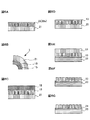

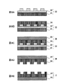

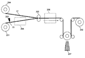


Classifications
-
- G—PHYSICS
- G02—OPTICS
- G02B—OPTICAL ELEMENTS, SYSTEMS OR APPARATUS
- G02B1/00—Optical elements characterised by the material of which they are made; Optical coatings for optical elements
- G02B1/10—Optical coatings produced by application to, or surface treatment of, optical elements
- G02B1/14—Protective coatings, e.g. hard coatings
-
- B—PERFORMING OPERATIONS; TRANSPORTING
- B32—LAYERED PRODUCTS
- B32B—LAYERED PRODUCTS, i.e. PRODUCTS BUILT-UP OF STRATA OF FLAT OR NON-FLAT, e.g. CELLULAR OR HONEYCOMB, FORM
- B32B3/00—Layered products comprising a layer with external or internal discontinuities or unevennesses, or a layer of non-planar shape; Layered products comprising a layer having particular features of form
- B32B3/26—Layered products comprising a layer with external or internal discontinuities or unevennesses, or a layer of non-planar shape; Layered products comprising a layer having particular features of form characterised by a particular shape of the outline of the cross-section of a continuous layer; characterised by a layer with cavities or internal voids ; characterised by an apertured layer
- B32B3/30—Layered products comprising a layer with external or internal discontinuities or unevennesses, or a layer of non-planar shape; Layered products comprising a layer having particular features of form characterised by a particular shape of the outline of the cross-section of a continuous layer; characterised by a layer with cavities or internal voids ; characterised by an apertured layer characterised by a layer formed with recesses or projections, e.g. hollows, grooves, protuberances, ribs
-
- B—PERFORMING OPERATIONS; TRANSPORTING
- B29—WORKING OF PLASTICS; WORKING OF SUBSTANCES IN A PLASTIC STATE IN GENERAL
- B29C—SHAPING OR JOINING OF PLASTICS; SHAPING OF MATERIAL IN A PLASTIC STATE, NOT OTHERWISE PROVIDED FOR; AFTER-TREATMENT OF THE SHAPED PRODUCTS, e.g. REPAIRING
- B29C59/00—Surface shaping of articles, e.g. embossing; Apparatus therefor
- B29C59/02—Surface shaping of articles, e.g. embossing; Apparatus therefor by mechanical means, e.g. pressing
-
- B—PERFORMING OPERATIONS; TRANSPORTING
- B32—LAYERED PRODUCTS
- B32B—LAYERED PRODUCTS, i.e. PRODUCTS BUILT-UP OF STRATA OF FLAT OR NON-FLAT, e.g. CELLULAR OR HONEYCOMB, FORM
- B32B27/00—Layered products comprising a layer of synthetic resin
- B32B27/30—Layered products comprising a layer of synthetic resin comprising vinyl (co)polymers; comprising acrylic (co)polymers
- B32B27/302—Layered products comprising a layer of synthetic resin comprising vinyl (co)polymers; comprising acrylic (co)polymers comprising aromatic vinyl (co)polymers, e.g. styrenic (co)polymers
-
- C—CHEMISTRY; METALLURGY
- C23—COATING METALLIC MATERIAL; COATING MATERIAL WITH METALLIC MATERIAL; CHEMICAL SURFACE TREATMENT; DIFFUSION TREATMENT OF METALLIC MATERIAL; COATING BY VACUUM EVAPORATION, BY SPUTTERING, BY ION IMPLANTATION OR BY CHEMICAL VAPOUR DEPOSITION, IN GENERAL; INHIBITING CORROSION OF METALLIC MATERIAL OR INCRUSTATION IN GENERAL
- C23C—COATING METALLIC MATERIAL; COATING MATERIAL WITH METALLIC MATERIAL; SURFACE TREATMENT OF METALLIC MATERIAL BY DIFFUSION INTO THE SURFACE, BY CHEMICAL CONVERSION OR SUBSTITUTION; COATING BY VACUUM EVAPORATION, BY SPUTTERING, BY ION IMPLANTATION OR BY CHEMICAL VAPOUR DEPOSITION, IN GENERAL
- C23C18/00—Chemical coating by decomposition of either liquid compounds or solutions of the coating forming compounds, without leaving reaction products of surface material in the coating; Contact plating
- C23C18/02—Chemical coating by decomposition of either liquid compounds or solutions of the coating forming compounds, without leaving reaction products of surface material in the coating; Contact plating by thermal decomposition
- C23C18/12—Chemical coating by decomposition of either liquid compounds or solutions of the coating forming compounds, without leaving reaction products of surface material in the coating; Contact plating by thermal decomposition characterised by the deposition of inorganic material other than metallic material
- C23C18/1204—Chemical coating by decomposition of either liquid compounds or solutions of the coating forming compounds, without leaving reaction products of surface material in the coating; Contact plating by thermal decomposition characterised by the deposition of inorganic material other than metallic material inorganic material, e.g. non-oxide and non-metallic such as sulfides, nitrides based compounds
- C23C18/1208—Oxides, e.g. ceramics
- C23C18/1216—Metal oxides
-
- C—CHEMISTRY; METALLURGY
- C23—COATING METALLIC MATERIAL; COATING MATERIAL WITH METALLIC MATERIAL; CHEMICAL SURFACE TREATMENT; DIFFUSION TREATMENT OF METALLIC MATERIAL; COATING BY VACUUM EVAPORATION, BY SPUTTERING, BY ION IMPLANTATION OR BY CHEMICAL VAPOUR DEPOSITION, IN GENERAL; INHIBITING CORROSION OF METALLIC MATERIAL OR INCRUSTATION IN GENERAL
- C23C—COATING METALLIC MATERIAL; COATING MATERIAL WITH METALLIC MATERIAL; SURFACE TREATMENT OF METALLIC MATERIAL BY DIFFUSION INTO THE SURFACE, BY CHEMICAL CONVERSION OR SUBSTITUTION; COATING BY VACUUM EVAPORATION, BY SPUTTERING, BY ION IMPLANTATION OR BY CHEMICAL VAPOUR DEPOSITION, IN GENERAL
- C23C18/00—Chemical coating by decomposition of either liquid compounds or solutions of the coating forming compounds, without leaving reaction products of surface material in the coating; Contact plating
- C23C18/02—Chemical coating by decomposition of either liquid compounds or solutions of the coating forming compounds, without leaving reaction products of surface material in the coating; Contact plating by thermal decomposition
- C23C18/12—Chemical coating by decomposition of either liquid compounds or solutions of the coating forming compounds, without leaving reaction products of surface material in the coating; Contact plating by thermal decomposition characterised by the deposition of inorganic material other than metallic material
- C23C18/1204—Chemical coating by decomposition of either liquid compounds or solutions of the coating forming compounds, without leaving reaction products of surface material in the coating; Contact plating by thermal decomposition characterised by the deposition of inorganic material other than metallic material inorganic material, e.g. non-oxide and non-metallic such as sulfides, nitrides based compounds
- C23C18/122—Inorganic polymers, e.g. silanes, polysilazanes, polysiloxanes
-
- C—CHEMISTRY; METALLURGY
- C23—COATING METALLIC MATERIAL; COATING MATERIAL WITH METALLIC MATERIAL; CHEMICAL SURFACE TREATMENT; DIFFUSION TREATMENT OF METALLIC MATERIAL; COATING BY VACUUM EVAPORATION, BY SPUTTERING, BY ION IMPLANTATION OR BY CHEMICAL VAPOUR DEPOSITION, IN GENERAL; INHIBITING CORROSION OF METALLIC MATERIAL OR INCRUSTATION IN GENERAL
- C23C—COATING METALLIC MATERIAL; COATING MATERIAL WITH METALLIC MATERIAL; SURFACE TREATMENT OF METALLIC MATERIAL BY DIFFUSION INTO THE SURFACE, BY CHEMICAL CONVERSION OR SUBSTITUTION; COATING BY VACUUM EVAPORATION, BY SPUTTERING, BY ION IMPLANTATION OR BY CHEMICAL VAPOUR DEPOSITION, IN GENERAL
- C23C18/00—Chemical coating by decomposition of either liquid compounds or solutions of the coating forming compounds, without leaving reaction products of surface material in the coating; Contact plating
- C23C18/02—Chemical coating by decomposition of either liquid compounds or solutions of the coating forming compounds, without leaving reaction products of surface material in the coating; Contact plating by thermal decomposition
- C23C18/12—Chemical coating by decomposition of either liquid compounds or solutions of the coating forming compounds, without leaving reaction products of surface material in the coating; Contact plating by thermal decomposition characterised by the deposition of inorganic material other than metallic material
- C23C18/1229—Composition of the substrate
- C23C18/1233—Organic substrates
-
- C—CHEMISTRY; METALLURGY
- C23—COATING METALLIC MATERIAL; COATING MATERIAL WITH METALLIC MATERIAL; CHEMICAL SURFACE TREATMENT; DIFFUSION TREATMENT OF METALLIC MATERIAL; COATING BY VACUUM EVAPORATION, BY SPUTTERING, BY ION IMPLANTATION OR BY CHEMICAL VAPOUR DEPOSITION, IN GENERAL; INHIBITING CORROSION OF METALLIC MATERIAL OR INCRUSTATION IN GENERAL
- C23C—COATING METALLIC MATERIAL; COATING MATERIAL WITH METALLIC MATERIAL; SURFACE TREATMENT OF METALLIC MATERIAL BY DIFFUSION INTO THE SURFACE, BY CHEMICAL CONVERSION OR SUBSTITUTION; COATING BY VACUUM EVAPORATION, BY SPUTTERING, BY ION IMPLANTATION OR BY CHEMICAL VAPOUR DEPOSITION, IN GENERAL
- C23C18/00—Chemical coating by decomposition of either liquid compounds or solutions of the coating forming compounds, without leaving reaction products of surface material in the coating; Contact plating
- C23C18/02—Chemical coating by decomposition of either liquid compounds or solutions of the coating forming compounds, without leaving reaction products of surface material in the coating; Contact plating by thermal decomposition
- C23C18/12—Chemical coating by decomposition of either liquid compounds or solutions of the coating forming compounds, without leaving reaction products of surface material in the coating; Contact plating by thermal decomposition characterised by the deposition of inorganic material other than metallic material
- C23C18/1229—Composition of the substrate
- C23C18/1245—Inorganic substrates other than metallic
-
- G—PHYSICS
- G02—OPTICS
- G02B—OPTICAL ELEMENTS, SYSTEMS OR APPARATUS
- G02B1/00—Optical elements characterised by the material of which they are made; Optical coatings for optical elements
- G02B1/10—Optical coatings produced by application to, or surface treatment of, optical elements
-
- H—ELECTRICITY
- H01—ELECTRIC ELEMENTS
- H01L—SEMICONDUCTOR DEVICES NOT COVERED BY CLASS H10
- H01L21/00—Processes or apparatus adapted for the manufacture or treatment of semiconductor or solid state devices or of parts thereof
- H01L21/02—Manufacture or treatment of semiconductor devices or of parts thereof
- H01L21/027—Making masks on semiconductor bodies for further photolithographic processing not provided for in group H01L21/18 or H01L21/34
- H01L21/0271—Making masks on semiconductor bodies for further photolithographic processing not provided for in group H01L21/18 or H01L21/34 comprising organic layers
- H01L21/0273—Making masks on semiconductor bodies for further photolithographic processing not provided for in group H01L21/18 or H01L21/34 comprising organic layers characterised by the treatment of photoresist layers
-
- H—ELECTRICITY
- H01—ELECTRIC ELEMENTS
- H01L—SEMICONDUCTOR DEVICES NOT COVERED BY CLASS H10
- H01L31/00—Semiconductor devices sensitive to infrared radiation, light, electromagnetic radiation of shorter wavelength or corpuscular radiation and specially adapted either for the conversion of the energy of such radiation into electrical energy or for the control of electrical energy by such radiation; Processes or apparatus specially adapted for the manufacture or treatment thereof or of parts thereof; Details thereof
- H01L31/02—Details
- H01L31/0236—Special surface textures
- H01L31/02366—Special surface textures of the substrate or of a layer on the substrate, e.g. textured ITO/glass substrate or superstrate, textured polymer layer on glass substrate
-
- Y—GENERAL TAGGING OF NEW TECHNOLOGICAL DEVELOPMENTS; GENERAL TAGGING OF CROSS-SECTIONAL TECHNOLOGIES SPANNING OVER SEVERAL SECTIONS OF THE IPC; TECHNICAL SUBJECTS COVERED BY FORMER USPC CROSS-REFERENCE ART COLLECTIONS [XRACs] AND DIGESTS
- Y02—TECHNOLOGIES OR APPLICATIONS FOR MITIGATION OR ADAPTATION AGAINST CLIMATE CHANGE
- Y02E—REDUCTION OF GREENHOUSE GAS [GHG] EMISSIONS, RELATED TO ENERGY GENERATION, TRANSMISSION OR DISTRIBUTION
- Y02E10/00—Energy generation through renewable energy sources
- Y02E10/50—Photovoltaic [PV] energy
-
- Y—GENERAL TAGGING OF NEW TECHNOLOGICAL DEVELOPMENTS; GENERAL TAGGING OF CROSS-SECTIONAL TECHNOLOGIES SPANNING OVER SEVERAL SECTIONS OF THE IPC; TECHNICAL SUBJECTS COVERED BY FORMER USPC CROSS-REFERENCE ART COLLECTIONS [XRACs] AND DIGESTS
- Y10—TECHNICAL SUBJECTS COVERED BY FORMER USPC
- Y10T—TECHNICAL SUBJECTS COVERED BY FORMER US CLASSIFICATION
- Y10T428/00—Stock material or miscellaneous articles
- Y10T428/24—Structurally defined web or sheet [e.g., overall dimension, etc.]
- Y10T428/24479—Structurally defined web or sheet [e.g., overall dimension, etc.] including variation in thickness
- Y10T428/24521—Structurally defined web or sheet [e.g., overall dimension, etc.] including variation in thickness with component conforming to contour of nonplanar surface
- Y10T428/24537—Parallel ribs and/or grooves
Landscapes
- Chemical & Material Sciences (AREA)
- Engineering & Computer Science (AREA)
- Physics & Mathematics (AREA)
- Mechanical Engineering (AREA)
- Organic Chemistry (AREA)
- General Chemical & Material Sciences (AREA)
- Chemical Kinetics & Catalysis (AREA)
- Inorganic Chemistry (AREA)
- Materials Engineering (AREA)
- Thermal Sciences (AREA)
- Metallurgy (AREA)
- General Physics & Mathematics (AREA)
- Microelectronics & Electronic Packaging (AREA)
- Condensed Matter Physics & Semiconductors (AREA)
- Computer Hardware Design (AREA)
- Power Engineering (AREA)
- Ceramic Engineering (AREA)
- Electromagnetism (AREA)
- Optics & Photonics (AREA)
- Manufacturing & Machinery (AREA)
- Laminated Bodies (AREA)
- Shaping Of Tube Ends By Bending Or Straightening (AREA)
- Electroluminescent Light Sources (AREA)
- Photovoltaic Devices (AREA)
Priority Applications (1)
| Application Number | Priority Date | Filing Date | Title |
|---|---|---|---|
| JP2012547902A JP5597263B2 (ja) | 2010-12-09 | 2011-12-08 | 微細構造積層体、微細構造積層体の作製方法及び微細構造体の製造方法 |
Applications Claiming Priority (12)
| Application Number | Priority Date | Filing Date | Title |
|---|---|---|---|
| JP2010274606 | 2010-12-09 | ||
| JP2010274606 | 2010-12-09 | ||
| JP2010274605 | 2010-12-09 | ||
| JP2010274935 | 2010-12-09 | ||
| JP2010274935 | 2010-12-09 | ||
| JP2010274605 | 2010-12-09 | ||
| JP2010282061 | 2010-12-17 | ||
| JP2010282061 | 2010-12-17 | ||
| JP2011004869 | 2011-01-13 | ||
| JP2011004869 | 2011-01-13 | ||
| JP2012547902A JP5597263B2 (ja) | 2010-12-09 | 2011-12-08 | 微細構造積層体、微細構造積層体の作製方法及び微細構造体の製造方法 |
| PCT/JP2011/078374 WO2012077738A1 (fr) | 2010-12-09 | 2011-12-08 | Stratifié à structure fine, procédé de préparation d'un stratifié à structure fine et procédé de production d'un stratifié à structure fine |
Publications (2)
| Publication Number | Publication Date |
|---|---|
| JPWO2012077738A1 JPWO2012077738A1 (ja) | 2014-05-22 |
| JP5597263B2 true JP5597263B2 (ja) | 2014-10-01 |
Family
ID=46207221
Family Applications (1)
| Application Number | Title | Priority Date | Filing Date |
|---|---|---|---|
| JP2012547902A Active JP5597263B2 (ja) | 2010-12-09 | 2011-12-08 | 微細構造積層体、微細構造積層体の作製方法及び微細構造体の製造方法 |
Country Status (9)
| Country | Link |
|---|---|
| US (1) | US9513409B2 (fr) |
| EP (1) | EP2650124B1 (fr) |
| JP (1) | JP5597263B2 (fr) |
| KR (1) | KR101565221B1 (fr) |
| CN (1) | CN103249562B (fr) |
| BR (1) | BR112013014167A2 (fr) |
| MY (1) | MY164197A (fr) |
| TW (1) | TWI458634B (fr) |
| WO (1) | WO2012077738A1 (fr) |
Families Citing this family (53)
| Publication number | Priority date | Publication date | Assignee | Title |
|---|---|---|---|---|
| JP5710236B2 (ja) * | 2010-12-17 | 2015-04-30 | 旭化成イーマテリアルズ株式会社 | 微細構造積層体 |
| CN104155847A (zh) * | 2011-06-21 | 2014-11-19 | 旭化成电子材料株式会社 | 微细凹凸结构转印用无机组合物 |
| US9780335B2 (en) | 2012-07-20 | 2017-10-03 | 3M Innovative Properties Company | Structured lamination transfer films and methods |
| JP6092561B2 (ja) * | 2012-10-01 | 2017-03-08 | 東芝機械株式会社 | 被成形体組立体、被成形体組立体の製造装置および被成形体組立体の製造方法 |
| JP2014093385A (ja) * | 2012-11-02 | 2014-05-19 | Fujifilm Corp | インプリント用密着膜の製造方法およびパターン形成方法 |
| FR2997966B1 (fr) | 2012-11-13 | 2020-08-14 | Seb Sa | Article en fonte d'acier comprenant un revetement vitreux et procede de fabrication d'un tel article |
| US9711744B2 (en) | 2012-12-21 | 2017-07-18 | 3M Innovative Properties Company | Patterned structured transfer tape |
| JP6132545B2 (ja) * | 2012-12-21 | 2017-05-24 | 旭化成株式会社 | 微細パタン形成用積層体 |
| US20140175707A1 (en) | 2012-12-21 | 2014-06-26 | 3M Innovative Properties Company | Methods of using nanostructured transfer tape and articles made therefrom |
| US20140242343A1 (en) * | 2013-02-27 | 2014-08-28 | 3M Innovative Properties Company | Lamination transfer films for forming embedded nanostructures |
| EP3427968B2 (fr) * | 2013-03-12 | 2023-03-01 | Toppan Printing Co., Ltd. | Representation |
| JP6047038B2 (ja) * | 2013-03-12 | 2016-12-21 | 株式会社カネカ | 有機el装置 |
| US9324966B2 (en) * | 2013-03-15 | 2016-04-26 | E I Du Pont De Nemours And Company | Thin-film transparent conductive structure and devices made therewith |
| AU2014258629B2 (en) * | 2013-04-26 | 2016-09-29 | Jx Nippon Oil & Energy Corporation | Substrate having rugged structure obtained from hydrophobic sol/gel material |
| CA2918872A1 (fr) * | 2013-07-26 | 2015-01-29 | Jx Nippon Oil & Energy Corporation | Procede de fabrication d'un substrat presentant une structure texturee |
| TWI529985B (zh) | 2013-12-27 | 2016-04-11 | 國立清華大學 | 提升壓電高分子電性輸出方法及壓電/導電混合高分子薄膜製程 |
| US9246134B2 (en) | 2014-01-20 | 2016-01-26 | 3M Innovative Properties Company | Lamination transfer films for forming articles with engineered voids |
| KR102350809B1 (ko) | 2014-01-20 | 2022-01-14 | 쓰리엠 이노베이티브 프로퍼티즈 컴파니 | 요각 구조체를 형성하기 위한 라미네이션 전사 필름 |
| US10513881B2 (en) | 2014-01-22 | 2019-12-24 | 3M Innovative Properties Company | Microoptics for glazing |
| WO2015136733A1 (fr) * | 2014-03-14 | 2015-09-17 | シャープ株式会社 | Élément optique et dispositif d'affichage |
| TW201539736A (zh) | 2014-03-19 | 2015-10-16 | 3M Innovative Properties Co | 用於藉白光成色之 oled 裝置的奈米結構 |
| DE102014104513A1 (de) * | 2014-03-31 | 2015-10-01 | Evonik Degussa Gmbh | Polymerzusammensetzung, Faserverbundhalbzeug und Verfahren zur Herstellung desselben |
| WO2015179152A1 (fr) * | 2014-05-20 | 2015-11-26 | Whitford Corporation | Compositions sol-gel à dureté et résistance aux chocs améliorées |
| CN104064488B (zh) * | 2014-06-12 | 2016-08-17 | 江阴新顺微电子有限公司 | 检测半导体芯片背面金属层分离的方法 |
| US9472788B2 (en) | 2014-08-27 | 2016-10-18 | 3M Innovative Properties Company | Thermally-assisted self-assembly method of nanoparticles and nanowires within engineered periodic structures |
| KR20170072272A (ko) | 2014-10-20 | 2017-06-26 | 쓰리엠 이노베이티브 프로퍼티즈 컴파니 | 미세구조화된 확산기를 포함하는 단열 글레이징 유닛 및 미세광학 층, 및 방법 |
| JP6441036B2 (ja) * | 2014-11-13 | 2018-12-19 | 旭化成株式会社 | 転写方法 |
| FR3028664B1 (fr) * | 2014-11-14 | 2016-11-25 | Soitec Silicon On Insulator | Procede de separation et de transfert de couches |
| US10518512B2 (en) | 2015-03-31 | 2019-12-31 | 3M Innovative Properties Company | Method of forming dual-cure nanostructure transfer film |
| US10106643B2 (en) | 2015-03-31 | 2018-10-23 | 3M Innovative Properties Company | Dual-cure nanostructure transfer film |
| CN107429113A (zh) * | 2015-03-31 | 2017-12-01 | 捷恩智株式会社 | 涂布剂、皮膜、层叠体、表面保护物品 |
| US10534120B2 (en) * | 2015-04-03 | 2020-01-14 | Moxtek, Inc. | Wire grid polarizer with protected wires |
| US9995864B2 (en) | 2015-04-03 | 2018-06-12 | Moxtek, Inc. | Wire grid polarizer with silane protective coating |
| KR101781976B1 (ko) * | 2015-04-08 | 2017-10-23 | 한국과학기술연구원 | 나노구조 하이브리드 입자 및 그 제조방법, 그리고 상기 입자를 포함하는 장치 |
| JP6492904B2 (ja) * | 2015-04-08 | 2019-04-03 | ダイキン工業株式会社 | 成形体 |
| WO2017079274A1 (fr) | 2015-11-02 | 2017-05-11 | Metashield Llc | Compositions à base de nanosilice, structures et appareil incorporant celles-ci et procédés associés |
| US9899239B2 (en) * | 2015-11-06 | 2018-02-20 | Apple Inc. | Carrier ultra thin substrate |
| CN108291998A (zh) * | 2015-11-23 | 2018-07-17 | 康宁股份有限公司 | 线栅偏振器及其制造方法 |
| TWI624428B (zh) * | 2016-04-01 | 2018-05-21 | 鈺冠科技股份有限公司 | 使用奈米材料的基板結構及其製作方法 |
| US10408983B2 (en) | 2016-08-16 | 2019-09-10 | Moxtek, Inc. | Durable, high performance wire grid polarizer having permeable junction between top protection layer |
| KR101902790B1 (ko) * | 2016-10-31 | 2018-10-01 | 재단법인 나노기반소프트일렉트로닉스연구단 | 고분자층/전도층을 포함하는 적층체, 그를 포함하는 고민감성 및 선형 민감성을 갖는 압력 센서, 및 그의 제조 방법 |
| JP6348951B2 (ja) * | 2016-11-18 | 2018-06-27 | 旭化成株式会社 | ロールモールドの製造方法 |
| EP3406752B1 (fr) * | 2017-05-22 | 2023-11-08 | Novaled GmbH | Procédé de préparation d'un dispositif électronique |
| EP3685989B1 (fr) * | 2017-09-22 | 2023-03-15 | Konica Minolta, Inc. | Accessoire de saisie d'objets et robot industriel utilisant un accessoire de saisie d'objets |
| CN109554133A (zh) * | 2017-09-26 | 2019-04-02 | 上海纳尔实业股份有限公司 | 一种防指纹tpu保护膜 |
| WO2019119189A1 (fr) * | 2017-12-18 | 2019-06-27 | Agency For Science, Technology And Research | Adhésif ayant une adhérence accrue |
| CN112020770A (zh) | 2018-04-16 | 2020-12-01 | 应用材料公司 | 使用暂时及永久接合的多层堆叠光学元件 |
| US20210292570A1 (en) | 2018-08-31 | 2021-09-23 | 3M Innovative Properties Company | Articles including nanostructured surfaces and interpenetrating layers, and methods of making same |
| CN111019476A (zh) * | 2019-12-11 | 2020-04-17 | 中国地质大学(武汉) | 一种超疏水和光催化油漆及其制备方法 |
| US11434394B2 (en) | 2020-05-14 | 2022-09-06 | The Procter & Gamble Company | Adhesive having increased bonding strength |
| KR102419282B1 (ko) * | 2020-09-11 | 2022-07-12 | 한국전자기술연구원 | 나노구조 광학필름을 이용한 태양전지 모듈 및 이의 제조방법 |
| CN112186121B (zh) * | 2020-10-06 | 2022-08-09 | 深圳市中升薄膜材料有限公司 | 一种用于amoled显示面板的复合光学膜 |
| JP7549519B2 (ja) | 2020-12-21 | 2024-09-11 | シャープ株式会社 | フィルム |
Citations (7)
| Publication number | Priority date | Publication date | Assignee | Title |
|---|---|---|---|---|
| JP2005047080A (ja) * | 2003-07-31 | 2005-02-24 | Alps Electric Co Ltd | 微細凹凸面を有する樹脂製光学部品成形用型及びこれを用いた樹脂製光学部品の製造方法 |
| JP2008503364A (ja) * | 2004-05-24 | 2008-02-07 | エージェンシー フォー サイエンス,テクノロジー アンド リサーチ | 支持された、および独立した3次元のマイクロまたはナノ構造体のインプリント方法 |
| JP2008068611A (ja) * | 2006-06-30 | 2008-03-27 | Asml Netherlands Bv | インプリントリソグラフィ |
| JP2008162190A (ja) * | 2006-12-28 | 2008-07-17 | Asahi Glass Co Ltd | 微細構造体の製造方法 |
| JP2009045925A (ja) * | 2007-07-23 | 2009-03-05 | Asahi Glass Co Ltd | ナノインプリント用モールドおよびその製造方法 |
| JP2010049745A (ja) * | 2008-08-21 | 2010-03-04 | Fuji Electric Device Technology Co Ltd | ナノインプリント用モールドおよびこれを用いて作製された磁気記録媒体 |
| WO2011111741A1 (fr) * | 2010-03-10 | 2011-09-15 | 旭化成株式会社 | Moule en résine |
Family Cites Families (24)
| Publication number | Priority date | Publication date | Assignee | Title |
|---|---|---|---|---|
| JPS6029349B2 (ja) * | 1978-10-06 | 1985-07-10 | 大日本印刷株式会社 | 化粧材の製造法 |
| CA2083865C (fr) * | 1991-12-04 | 1998-09-29 | Masahiko Sekiya | Substrat de support d'enregistrement optique et support magneto-optique utilisant ce substitut |
| US6342434B1 (en) * | 1995-12-04 | 2002-01-29 | Hitachi, Ltd. | Methods of processing semiconductor wafer, and producing IC card, and carrier |
| US6280861B1 (en) * | 1996-05-29 | 2001-08-28 | Idemitsu Kosan Co., Ltd. | Organic EL device |
| US6523803B1 (en) * | 1998-09-03 | 2003-02-25 | Micron Technology, Inc. | Mold apparatus used during semiconductor device fabrication |
| US6335479B1 (en) * | 1998-10-13 | 2002-01-01 | Dai Nippon Printing Co., Ltd. | Protective sheet for solar battery module, method of fabricating the same and solar battery module |
| US6535680B1 (en) * | 1999-09-16 | 2003-03-18 | Nippon Sheet Glass Co., Ltd. | Process for producing an article having a predetermined surface shape and optical waveguide element |
| JP2003004916A (ja) | 2001-06-20 | 2003-01-08 | Dainippon Printing Co Ltd | 表示装置の窓材、その製造方法、及び表示装置 |
| US7006291B2 (en) * | 2002-07-31 | 2006-02-28 | Nippon Sheet Glass Co., Ltd. | Optical device and method for fabricating the same |
| JP4447203B2 (ja) | 2002-09-05 | 2010-04-07 | 大日本印刷株式会社 | パターン形成体 |
| US7143609B2 (en) | 2002-10-29 | 2006-12-05 | Corning Incorporated | Low-temperature fabrication of glass optical components |
| KR100509437B1 (ko) * | 2003-01-27 | 2005-08-26 | 주식회사 에너랜드 | 적층형 리튬이차전지 및 그 제조방법 |
| US20050023433A1 (en) | 2003-07-31 | 2005-02-03 | Alps Electric Co., Ltd. | Resin optical component mold having minute concavo-convex portions and method of manufacturing resin optical component using the same |
| JP4606775B2 (ja) | 2004-05-25 | 2011-01-05 | 電源開発株式会社 | 凹型酸化膜構造体 |
| TW200700793A (en) * | 2005-06-20 | 2007-01-01 | Exploit Technology Co Ltd | Screen protection film with anti-flicker, anti-dizzying, scratch-resistant functions and manufacturing method thereof |
| TWM317021U (en) * | 2006-12-28 | 2007-08-11 | Eternal Chemical Co Ltd | Composite optical film |
| JP4930517B2 (ja) | 2007-02-07 | 2012-05-16 | 旭硝子株式会社 | インプリント用モールドおよびその製造方法 |
| JP5359871B2 (ja) | 2007-06-20 | 2013-12-04 | 旭硝子株式会社 | フッ素化剤による酸化物ガラスの表面処理方法 |
| JP2009003331A (ja) * | 2007-06-25 | 2009-01-08 | Toppan Printing Co Ltd | 防眩フィルム |
| JP2009020288A (ja) * | 2007-07-11 | 2009-01-29 | Sony Corp | 防眩性フィルムおよびその製造方法、偏光子ならびに表示装置 |
| JP2009042925A (ja) | 2007-08-07 | 2009-02-26 | Panasonic Corp | コンテンツ利用方法、永続視聴ライセンスの有効性の判断方法、ダウンロード端末、サーバ、ダウンロードシステム、コンテンツの管理方法、プログラム及び記録媒体 |
| JP5261817B2 (ja) | 2008-08-30 | 2013-08-14 | 国立大学法人長岡技術科学大学 | 表面に微細凹凸パターンを有したセラミックス焼成体及びその製造方法 |
| TW201015159A (en) * | 2008-10-02 | 2010-04-16 | Gigastorage Corp | Structure for multi-layer coating composite optical film |
| EP2453485A1 (fr) * | 2009-07-09 | 2012-05-16 | LINTEC Corporation | Feuille de protection pour module de cellule solaire |
-
2011
- 2011-12-08 TW TW100145371A patent/TWI458634B/zh not_active IP Right Cessation
- 2011-12-08 CN CN201180059183.9A patent/CN103249562B/zh not_active Expired - Fee Related
- 2011-12-08 EP EP11846133.4A patent/EP2650124B1/fr not_active Not-in-force
- 2011-12-08 MY MYPI2013002099A patent/MY164197A/en unknown
- 2011-12-08 BR BR112013014167A patent/BR112013014167A2/pt not_active Application Discontinuation
- 2011-12-08 KR KR1020137012558A patent/KR101565221B1/ko active IP Right Grant
- 2011-12-08 JP JP2012547902A patent/JP5597263B2/ja active Active
- 2011-12-08 US US13/992,581 patent/US9513409B2/en not_active Expired - Fee Related
- 2011-12-08 WO PCT/JP2011/078374 patent/WO2012077738A1/fr active Application Filing
Patent Citations (8)
| Publication number | Priority date | Publication date | Assignee | Title |
|---|---|---|---|---|
| JP2005047080A (ja) * | 2003-07-31 | 2005-02-24 | Alps Electric Co Ltd | 微細凹凸面を有する樹脂製光学部品成形用型及びこれを用いた樹脂製光学部品の製造方法 |
| JP2008503364A (ja) * | 2004-05-24 | 2008-02-07 | エージェンシー フォー サイエンス,テクノロジー アンド リサーチ | 支持された、および独立した3次元のマイクロまたはナノ構造体のインプリント方法 |
| JP2008068611A (ja) * | 2006-06-30 | 2008-03-27 | Asml Netherlands Bv | インプリントリソグラフィ |
| JP2008162190A (ja) * | 2006-12-28 | 2008-07-17 | Asahi Glass Co Ltd | 微細構造体の製造方法 |
| JP2009045925A (ja) * | 2007-07-23 | 2009-03-05 | Asahi Glass Co Ltd | ナノインプリント用モールドおよびその製造方法 |
| JP2010049745A (ja) * | 2008-08-21 | 2010-03-04 | Fuji Electric Device Technology Co Ltd | ナノインプリント用モールドおよびこれを用いて作製された磁気記録媒体 |
| WO2011111741A1 (fr) * | 2010-03-10 | 2011-09-15 | 旭化成株式会社 | Moule en résine |
| JP2011207221A (ja) * | 2010-03-10 | 2011-10-20 | Asahi Kasei E-Materials Corp | 樹脂モールド |
Also Published As
| Publication number | Publication date |
|---|---|
| TW201236872A (en) | 2012-09-16 |
| EP2650124A1 (fr) | 2013-10-16 |
| EP2650124B1 (fr) | 2019-05-15 |
| MY164197A (en) | 2017-11-30 |
| BR112013014167A2 (pt) | 2016-09-13 |
| CN103249562B (zh) | 2015-07-08 |
| KR101565221B1 (ko) | 2015-11-02 |
| JPWO2012077738A1 (ja) | 2014-05-22 |
| KR20130080857A (ko) | 2013-07-15 |
| CN103249562A (zh) | 2013-08-14 |
| WO2012077738A1 (fr) | 2012-06-14 |
| US20130319522A1 (en) | 2013-12-05 |
| TWI458634B (zh) | 2014-11-01 |
| EP2650124A4 (fr) | 2014-04-30 |
| US9513409B2 (en) | 2016-12-06 |
Similar Documents
| Publication | Publication Date | Title |
|---|---|---|
| JP5597263B2 (ja) | 微細構造積層体、微細構造積層体の作製方法及び微細構造体の製造方法 | |
| US10766169B2 (en) | Resin mold | |
| KR101326614B1 (ko) | 미세 패턴 형성용 적층체 및 미세 패턴 형성용 적층체의 제조 방법 | |
| JP5277357B2 (ja) | 微細凹凸構造転写用無機組成物 | |
| WO2013002048A1 (fr) | Gabarit de transcription de microstructure convexo-concave | |
| JP5658001B2 (ja) | 樹脂モールド | |
| JP5956198B2 (ja) | 集光型太陽電池用レンズ及び集光型太陽電池用レンズの製造方法 | |
| JP5813418B2 (ja) | 微細パターンの製造方法 | |
| JP5990411B2 (ja) | 防塵膜の製造方法 | |
| JP2012101483A (ja) | 樹脂モールド製造方法 | |
| JP6132545B2 (ja) | 微細パタン形成用積層体 |
Legal Events
| Date | Code | Title | Description |
|---|---|---|---|
| A131 | Notification of reasons for refusal |
Free format text: JAPANESE INTERMEDIATE CODE: A131 Effective date: 20140617 |
|
| A521 | Request for written amendment filed |
Free format text: JAPANESE INTERMEDIATE CODE: A523 Effective date: 20140714 |
|
| TRDD | Decision of grant or rejection written | ||
| A01 | Written decision to grant a patent or to grant a registration (utility model) |
Free format text: JAPANESE INTERMEDIATE CODE: A01 Effective date: 20140805 |
|
| A61 | First payment of annual fees (during grant procedure) |
Free format text: JAPANESE INTERMEDIATE CODE: A61 Effective date: 20140808 |
|
| R150 | Certificate of patent or registration of utility model |
Ref document number: 5597263 Country of ref document: JP Free format text: JAPANESE INTERMEDIATE CODE: R150 |
|
| S111 | Request for change of ownership or part of ownership |
Free format text: JAPANESE INTERMEDIATE CODE: R313111 |
|
| R350 | Written notification of registration of transfer |
Free format text: JAPANESE INTERMEDIATE CODE: R350 |
|
| S801 | Written request for registration of abandonment of right |
Free format text: JAPANESE INTERMEDIATE CODE: R311801 |
|
| ABAN | Cancellation due to abandonment | ||
| R350 | Written notification of registration of transfer |
Free format text: JAPANESE INTERMEDIATE CODE: R350 |