JP5491906B2 - 束状フレキシブル配線 - Google Patents
束状フレキシブル配線 Download PDFInfo
- Publication number
- JP5491906B2 JP5491906B2 JP2010044117A JP2010044117A JP5491906B2 JP 5491906 B2 JP5491906 B2 JP 5491906B2 JP 2010044117 A JP2010044117 A JP 2010044117A JP 2010044117 A JP2010044117 A JP 2010044117A JP 5491906 B2 JP5491906 B2 JP 5491906B2
- Authority
- JP
- Japan
- Prior art keywords
- section
- bundle
- connection section
- flexible substrate
- layer
- Prior art date
- Legal status (The legal status is an assumption and is not a legal conclusion. Google has not performed a legal analysis and makes no representation as to the accuracy of the status listed.)
- Active
Links
- 239000000758 substrate Substances 0.000 claims description 40
- 238000004804 winding Methods 0.000 claims description 39
- 239000000463 material Substances 0.000 claims description 13
- 230000002265 prevention Effects 0.000 claims description 6
- 230000000694 effects Effects 0.000 description 5
- 238000003780 insertion Methods 0.000 description 5
- 230000037431 insertion Effects 0.000 description 5
- 230000008054 signal transmission Effects 0.000 description 4
- 239000004020 conductor Substances 0.000 description 3
- 230000005540 biological transmission Effects 0.000 description 2
- 239000011810 insulating material Substances 0.000 description 2
- 238000012986 modification Methods 0.000 description 2
- 230000004048 modification Effects 0.000 description 2
- RYGMFSIKBFXOCR-UHFFFAOYSA-N Copper Chemical compound [Cu] RYGMFSIKBFXOCR-UHFFFAOYSA-N 0.000 description 1
- BQCADISMDOOEFD-UHFFFAOYSA-N Silver Chemical compound [Ag] BQCADISMDOOEFD-UHFFFAOYSA-N 0.000 description 1
- 229910052782 aluminium Inorganic materials 0.000 description 1
- XAGFODPZIPBFFR-UHFFFAOYSA-N aluminium Chemical compound [Al] XAGFODPZIPBFFR-UHFFFAOYSA-N 0.000 description 1
- 238000005452 bending Methods 0.000 description 1
- 238000004891 communication Methods 0.000 description 1
- 239000011889 copper foil Substances 0.000 description 1
- 238000010586 diagram Methods 0.000 description 1
- 238000005516 engineering process Methods 0.000 description 1
- 239000004744 fabric Substances 0.000 description 1
- 239000011888 foil Substances 0.000 description 1
- 238000009413 insulation Methods 0.000 description 1
- 229910052751 metal Inorganic materials 0.000 description 1
- 239000002184 metal Substances 0.000 description 1
Images


Classifications
-
- H—ELECTRICITY
- H05—ELECTRIC TECHNIQUES NOT OTHERWISE PROVIDED FOR
- H05K—PRINTED CIRCUITS; CASINGS OR CONSTRUCTIONAL DETAILS OF ELECTRIC APPARATUS; MANUFACTURE OF ASSEMBLAGES OF ELECTRICAL COMPONENTS
- H05K1/00—Printed circuits
- H05K1/02—Details
- H05K1/0277—Bendability or stretchability details
- H05K1/028—Bending or folding regions of flexible printed circuits
-
- H—ELECTRICITY
- H01—ELECTRIC ELEMENTS
- H01B—CABLES; CONDUCTORS; INSULATORS; SELECTION OF MATERIALS FOR THEIR CONDUCTIVE, INSULATING OR DIELECTRIC PROPERTIES
- H01B7/00—Insulated conductors or cables characterised by their form
- H01B7/08—Flat or ribbon cables
- H01B7/0892—Flat or ribbon cables incorporated in a cable of non-flat configuration
-
- H—ELECTRICITY
- H05—ELECTRIC TECHNIQUES NOT OTHERWISE PROVIDED FOR
- H05K—PRINTED CIRCUITS; CASINGS OR CONSTRUCTIONAL DETAILS OF ELECTRIC APPARATUS; MANUFACTURE OF ASSEMBLAGES OF ELECTRICAL COMPONENTS
- H05K1/00—Printed circuits
- H05K1/02—Details
- H05K1/0213—Electrical arrangements not otherwise provided for
- H05K1/0216—Reduction of cross-talk, noise or electromagnetic interference
- H05K1/0218—Reduction of cross-talk, noise or electromagnetic interference by printed shielding conductors, ground planes or power plane
-
- H—ELECTRICITY
- H05—ELECTRIC TECHNIQUES NOT OTHERWISE PROVIDED FOR
- H05K—PRINTED CIRCUITS; CASINGS OR CONSTRUCTIONAL DETAILS OF ELECTRIC APPARATUS; MANUFACTURE OF ASSEMBLAGES OF ELECTRICAL COMPONENTS
- H05K1/00—Printed circuits
- H05K1/02—Details
- H05K1/14—Structural association of two or more printed circuits
- H05K1/148—Arrangements of two or more hingeably connected rigid printed circuit boards, i.e. connected by flexible means
-
- H—ELECTRICITY
- H05—ELECTRIC TECHNIQUES NOT OTHERWISE PROVIDED FOR
- H05K—PRINTED CIRCUITS; CASINGS OR CONSTRUCTIONAL DETAILS OF ELECTRIC APPARATUS; MANUFACTURE OF ASSEMBLAGES OF ELECTRICAL COMPONENTS
- H05K1/00—Printed circuits
- H05K1/18—Printed circuits structurally associated with non-printed electric components
- H05K1/189—Printed circuits structurally associated with non-printed electric components characterised by the use of a flexible or folded printed circuit
-
- H—ELECTRICITY
- H05—ELECTRIC TECHNIQUES NOT OTHERWISE PROVIDED FOR
- H05K—PRINTED CIRCUITS; CASINGS OR CONSTRUCTIONAL DETAILS OF ELECTRIC APPARATUS; MANUFACTURE OF ASSEMBLAGES OF ELECTRICAL COMPONENTS
- H05K2201/00—Indexing scheme relating to printed circuits covered by H05K1/00
- H05K2201/05—Flexible printed circuits [FPCs]
- H05K2201/051—Rolled
-
- H—ELECTRICITY
- H05—ELECTRIC TECHNIQUES NOT OTHERWISE PROVIDED FOR
- H05K—PRINTED CIRCUITS; CASINGS OR CONSTRUCTIONAL DETAILS OF ELECTRIC APPARATUS; MANUFACTURE OF ASSEMBLAGES OF ELECTRICAL COMPONENTS
- H05K2201/00—Indexing scheme relating to printed circuits covered by H05K1/00
- H05K2201/05—Flexible printed circuits [FPCs]
- H05K2201/055—Folded back on itself
Landscapes
- Engineering & Computer Science (AREA)
- Microelectronics & Electronic Packaging (AREA)
- Shielding Devices Or Components To Electric Or Magnetic Fields (AREA)
- Structure Of Printed Boards (AREA)
- Insertion, Bundling And Securing Of Wires For Electric Apparatuses (AREA)
- Insulated Conductors (AREA)
- Manufacturing & Machinery (AREA)
Description
本発明のもう一つの目的は、折り畳み可能な構造にし、フレキシブル配線の端部の幅を小さくして回転軸の孔に通すことができる束状フレキシブル配線を提供することにある。
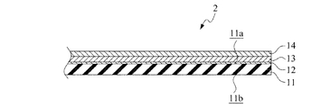
図1及び図2に示すように、本発明の第一実施形態による束状フレキシブル配線100は、延伸方向Iで所定長さ延伸したフレキシブル基板11を含む。
フレキシブル基板11は、第1の表面11a及び第2の表面11bを有する。
フレキシブル基板11の第1の表面11a上には、第1の導電層12及び第1の絶縁層13が順次形成されている。
第1の絶縁層13上には、遮蔽層14がさらに形成されている。
遮蔽層14は、第1の絶縁層13の表面上の所定領域を選択的に覆い、電気信号の電磁遮蔽効果を得る。
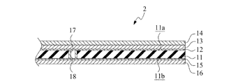
図3に示すように、両面の回路基板の構造では、フレキシブル基板11の第2の表面11bに、第2の導電層15及び第2の絶縁層16が順次形成されている。
また、両面の回路基板の構造では、信号ジャンパー構造が設けられている。
即ち、フレキシブル基板11の第1の表面11aと第2の表面11bとの間の所定位置には、貫通孔17が設けられている。
貫通孔17の内壁面には導電材料18が設けられ、フレキシブル基板11の第1の表面11a及び第2の表面11bの上に設けられた第1の導電層12及び第2の導電層15へ、信号を選択的に導通させる。
両面の回路基板は、2つの単面の回路基板を背中合わせで組み合わせた構造でもよい。
即ち、束ねセクション4には、一方の端部に第1の接続セクション2が設けられ、他方の端部に第2の接続セクション3が設けられている。
束ね線41の全部又は一部には、信号線が設けられ、第1の接続セクション2と第2の接続セクション3との間の電気信号の伝送ルートとして用いる。
束ねセクション4において、束ね線41の端部の適宜な箇所(例えば、第1の接続セクション2及び第2の接続セクション3の箇所)に、全部又は一部の切込みと、数個の切断防止孔214とを設け、フレキシブル基板11を組み立てたり使用したりするときに、束ね線41が切込みに沿って不用意に切れて損壊することを防ぐ。
図4及び図5に示すように、積層構造20は、中央領域21と、中央領域21の両側に設けられた側部積層領域22,23とを含む。
両側のうちの少なくとも1つの側部積層領域22,23は、実体又は仮想の折り線212,213に沿って折り曲げ、中央領域21に向かって重ねる。
側部積層領域22,23は、中央領域21の下方位置で重ねたり、中央領域21の一部の領域と重ねたりしてもよい。
これにより、第1の接続セクション2は、フレキシブル基板11の延伸方向Iに対する垂直方向(即ち、幅)が狭くなる。
第2の接続セクション3は、同様に中央領域31の両側に設けた側部積層領域32,33を中央領域31に重ねたり、中央領域31の一部の領域と重ねたりしてもよい。
図4は、重ねた後の構造である。
図1に示すように、本実施形態の第1の接続セクション2の中央領域21には、接続溝部211が設けられ、第2の接続セクション3の側部積層領域32の側部には、挿着端部321が設けられている。
当然、第1の接続セクション2及び第2の接続セクション3には、同じ態様の接続溝部又は挿着端部を設けてもよい。
図6に示すように、本実施形態の第1の接続セクション2の中央領域21には、接続溝部211が設けられ、第2の接続セクション3の側部積層領域32には、接続溝部311が設けられている。
図1に示すように、本実施形態の接続セクションは、単一の束ねセクションにより、他の接続セクションに接続されており、図7に示すように、本実施形態の第2の接続セクション3は、一方の束ねセクション4の束ね線41により、第1の接続セクション2と接続され、他方の束ねセクション4aの束ね線41aにより、第1の接続セクション2aと接続されている。
このように、束状フレキシブル配線の態様は必要に応じて変えることができる。
図8に示すように、本発明の一実施形態による巻付け構造5は遮蔽層51を有する。巻付け構造5は、遮蔽材料からなる巻付け構造を含み、束ねセクション4の所定位置に巻付け、束ねセクション4の各束ね線41を束状構造にし、電磁遮蔽効果を得る。
巻付け構造5には、絶縁材料(例えば、防水テープ)を用い、遮蔽材料と絶縁材料とを組み合わせ、巻付け構造を形成してもよい。
図9に示すように、本発明の一実施形態による束状フレキシブル配線100のフレキシブル基板11の束ねセクション4の束ね線41を、回転軸構造6に通した後、回転軸構造6の2つの対応した位置に、第1の接続セクション2及び第2の接続セクション3をそれぞれ配置する。
巻付け構造5の遮蔽層51により得られる電磁遮蔽効果により、束ねセクション4の束ね線41により信号を送信する際、ルートの中を通過するときに発生する可能性がある電磁波妨害を防ぐことができる。
例えば、図12に示すように、束状フレキシブル配線は、細長いシートの遮蔽材料を斜め巻付け方向IIIで、束ねセクション4の束ね線41に螺旋状で巻付け、螺旋状の巻付け構造5aが形成されている。
細長い遮蔽材料は、導電布、銀箔、アルミ箔、銅箔、金属シートなどの電磁遮蔽効果を備える材料から選択してもよい。
従って、本発明の特許請求の範囲は、このような変更や修正を含めて広く解釈されるべきである。
2a 第1の接続セクション
3 第2の接続セクション
4 束ねセクション
4a 束ねセクション
5 巻付け構造
5a 螺旋状の巻付け構造
6 回転軸構造
11 フレキシブル基板
11a 第1の表面
11b 第2の表面
12 第1の導電層
13 第1の絶縁層
14 遮蔽層
15 第2の導電層
16 第2の絶縁層
17 貫通孔
18 導電材料
20 積層構造
21 中央領域
22 側部積層領域
23 側部積層領域
31 中央領域
32 側部積層領域
33 側部積層領域
41 束ね線
41a 束ね線
51 遮蔽層
52 絶縁外層
53 絶縁内層
54 絶縁外層
100 束状フレキシブル配線
211 接続溝部
212 折り線
213 折り線
214 切断防止孔
311 接続溝部
321 挿着端部
I 延伸方向
II 巻付け方向
III 斜め巻付け方向
Claims (6)
- 延伸方向に延伸され、第1の表面及び第2の表面を有し、前記第1の表面は第1の導電層で形成され、第1の絶縁層が前記第1の導電層上に形成され、遮蔽層が前記第1の絶縁層上に形成されたフレキシブル基板と、
前記フレキシブル基板の一方の端部に設けられた少なくとも1つの第1の接続セクションと、
前記フレキシブル基板の他方の端部に設けられた少なくとも1つの第2の接続セクションと、
前記第1の接続セクションと前記第2の接続セクションとの間に設けられ、前記フレキシブル基板の延伸方向に沿って切込みが形成された複数の束ね線を含む少なくとも1つの束ねセクションと、
前記束ねセクションの所定位置に巻付けられ、前記束ねセクションの前記束ね線のそれぞれを巻付けて束状構造に形成した少なくとも1つの巻付け構造と、を備え、
前記第1の接続セクション及び前記第2の接続セクションのうちの少なくとも1つは、積層構造を含み、前記積層構造は、前記第1の接続セクションの両側部又は一方の側部を折り線に沿って折り曲げ、前記第1の接続セクションの中央領域の少なくとも一部の領域に前記側部を重ね、
全部又は一部の前記束ね線には、前記第1の接続セクション又は前記第2の接続セクションに隣接した所定箇所に、少なくとも1つの切断防止孔が設けられ、
前記巻付け構造は、
前記束ねセクションに巻付けられた電磁遮蔽材料層と、
前記電磁遮蔽材料層の外周に巻付けられた絶縁外層と、を有することを特徴とする、束状フレキシブル配線。 - 前記フレキシブル基板の前記第2の表面には、
第2の導電層と、
前記第2の導電層上に形成された第2の絶縁層と、が形成されていることを特徴とする請求項1に記載の束状フレキシブル配線。 - 前記巻付け構造は、前記束ねセクションの所定位置に巻付けられていることを特徴とする請求項1に記載の束状フレキシブル配線。
- 延伸方向に延伸され、第1の表面及び第2の表面を有し、前記第1の表面は第1の導電層で形成され、第1の絶縁層が前記第1の導電層上に形成され、遮蔽層が前記第1の絶縁層上に形成されたフレキシブル基板と、
前記フレキシブル基板の一方の端部に設けられた少なくとも1つの第1の接続セクションと、
前記フレキシブル基板の他方の端部に設けられた少なくとも1つの第2の接続セクションと、
前記第1の接続セクションと前記第2の接続セクションとの間に設けられ、前記フレキシブル基板の延伸方向に沿って切込みが形成された複数の束ね線を含む少なくとも1つの束ねセクションと、
前記束ねセクションの所定位置に巻付け、前記束ねセクションの前記束ね線のそれぞれを巻付け、束状構造を形成する少なくとも1つの巻付け構造と、を備え、
前記巻付け構造は、前記束ねセクションの前記所定位置に、巻付け方向で巻付けられたシート状体を有し、
全部又は一部の前記束ね線には、前記第1の接続セクション又は前記第2の接続セクションに隣接した所定箇所に、少なくとも1つの切断防止孔が設けられ、
前記巻付け構造は、
前記束ねセクションに巻付けられた電磁遮蔽材料層と、
前記電磁遮蔽材料層の外周に巻付けられた絶縁外層と、を有することを特徴とする束状フレキシブル配線。 - 前記フレキシブル基板の前記第2の表面には、
第2の導電層と、
前記第2の導電層に形成された第2の絶縁層と、が形成されていることを特徴とする請求項4に記載の束状フレキシブル配線。 - 前記巻付け構造は、前記束ねセクションの所定位置に巻付けられていることを特徴とする請求項4に記載の束状フレキシブル配線。
Applications Claiming Priority (2)
| Application Number | Priority Date | Filing Date | Title |
|---|---|---|---|
| TW098131522 | 2009-09-18 | ||
| TW098131522A TWI543209B (zh) | 2009-09-18 | 2009-09-18 | Bundled soft circuit cable |
Publications (3)
| Publication Number | Publication Date |
|---|---|
| JP2011066379A JP2011066379A (ja) | 2011-03-31 |
| JP2011066379A5 JP2011066379A5 (ja) | 2013-04-04 |
| JP5491906B2 true JP5491906B2 (ja) | 2014-05-14 |
Family
ID=43755649
Family Applications (1)
| Application Number | Title | Priority Date | Filing Date |
|---|---|---|---|
| JP2010044117A Active JP5491906B2 (ja) | 2009-09-18 | 2010-03-01 | 束状フレキシブル配線 |
Country Status (4)
| Country | Link |
|---|---|
| US (4) | US20110067903A1 (ja) |
| JP (1) | JP5491906B2 (ja) |
| KR (1) | KR101664241B1 (ja) |
| TW (1) | TWI543209B (ja) |
Families Citing this family (187)
| Publication number | Priority date | Publication date | Assignee | Title |
|---|---|---|---|---|
| JP2011066086A (ja) * | 2009-09-15 | 2011-03-31 | Toshiba Corp | フレキシブル配線板アレイとその製造方法及びフレキシブル配線装置 |
| US20110122323A1 (en) * | 2009-11-26 | 2011-05-26 | Samsung Electronics Co., Ltd. | Flat cable and display apparatus including the same |
| TWI537990B (zh) * | 2012-05-25 | 2016-06-11 | Adv Flexible Circuits Co Ltd | A soft circuit cable with two or more groups of clusters |
| TWI453768B (zh) * | 2012-06-20 | 2014-09-21 | Adv Flexible Circuits Co Ltd | Composite flexible circuit cable |
| TW201415743A (zh) * | 2012-10-09 | 2014-04-16 | Adv Flexible Circuits Co Ltd | 軟性電路排線之分束結構 |
| US9113347B2 (en) | 2012-12-05 | 2015-08-18 | At&T Intellectual Property I, Lp | Backhaul link for distributed antenna system |
| US10009065B2 (en) | 2012-12-05 | 2018-06-26 | At&T Intellectual Property I, L.P. | Backhaul link for distributed antenna system |
| CN103885531A (zh) * | 2012-12-22 | 2014-06-25 | 鸿富锦精密工业(深圳)有限公司 | 电子设备连接装置 |
| US9781825B2 (en) * | 2013-02-18 | 2017-10-03 | Dell Products L.P. | Flex circuit, an information handling system, and a method of manufacturing a flexible circuit |
| US9974187B2 (en) * | 2013-04-22 | 2018-05-15 | Infineon Technologies Austria Ag | Power in lead |
| US9999038B2 (en) | 2013-05-31 | 2018-06-12 | At&T Intellectual Property I, L.P. | Remote distributed antenna system |
| US9525524B2 (en) | 2013-05-31 | 2016-12-20 | At&T Intellectual Property I, L.P. | Remote distributed antenna system |
| TWI637669B (zh) * | 2013-07-12 | 2018-10-01 | 易鼎股份有限公司 | Wearable assembly method of flexible circuit board and shaft member |
| TWI590721B (zh) * | 2013-07-26 | 2017-07-01 | Adv Flexible Circuits Co Ltd | The flexible circuit board with the wings and the shaft assembly structure |
| US8897697B1 (en) | 2013-11-06 | 2014-11-25 | At&T Intellectual Property I, Lp | Millimeter-wave surface-wave communications |
| US9209902B2 (en) | 2013-12-10 | 2015-12-08 | At&T Intellectual Property I, L.P. | Quasi-optical coupler |
| TWI622328B (zh) * | 2014-03-03 | 2018-04-21 | Stretchable flexible circuit board | |
| TWI573503B (zh) * | 2014-06-09 | 2017-03-01 | The Power Supply Path Structure of Soft Circuit Board | |
| US9692101B2 (en) | 2014-08-26 | 2017-06-27 | At&T Intellectual Property I, L.P. | Guided wave couplers for coupling electromagnetic waves between a waveguide surface and a surface of a wire |
| US9768833B2 (en) | 2014-09-15 | 2017-09-19 | At&T Intellectual Property I, L.P. | Method and apparatus for sensing a condition in a transmission medium of electromagnetic waves |
| US10063280B2 (en) | 2014-09-17 | 2018-08-28 | At&T Intellectual Property I, L.P. | Monitoring and mitigating conditions in a communication network |
| US9628854B2 (en) | 2014-09-29 | 2017-04-18 | At&T Intellectual Property I, L.P. | Method and apparatus for distributing content in a communication network |
| US9615269B2 (en) | 2014-10-02 | 2017-04-04 | At&T Intellectual Property I, L.P. | Method and apparatus that provides fault tolerance in a communication network |
| US9685992B2 (en) | 2014-10-03 | 2017-06-20 | At&T Intellectual Property I, L.P. | Circuit panel network and methods thereof |
| US9503189B2 (en) | 2014-10-10 | 2016-11-22 | At&T Intellectual Property I, L.P. | Method and apparatus for arranging communication sessions in a communication system |
| US9762289B2 (en) | 2014-10-14 | 2017-09-12 | At&T Intellectual Property I, L.P. | Method and apparatus for transmitting or receiving signals in a transportation system |
| US9973299B2 (en) | 2014-10-14 | 2018-05-15 | At&T Intellectual Property I, L.P. | Method and apparatus for adjusting a mode of communication in a communication network |
| US9312919B1 (en) | 2014-10-21 | 2016-04-12 | At&T Intellectual Property I, Lp | Transmission device with impairment compensation and methods for use therewith |
| US9653770B2 (en) | 2014-10-21 | 2017-05-16 | At&T Intellectual Property I, L.P. | Guided wave coupler, coupling module and methods for use therewith |
| US9577306B2 (en) | 2014-10-21 | 2017-02-21 | At&T Intellectual Property I, L.P. | Guided-wave transmission device and methods for use therewith |
| US9769020B2 (en) | 2014-10-21 | 2017-09-19 | At&T Intellectual Property I, L.P. | Method and apparatus for responding to events affecting communications in a communication network |
| US9780834B2 (en) | 2014-10-21 | 2017-10-03 | At&T Intellectual Property I, L.P. | Method and apparatus for transmitting electromagnetic waves |
| US9520945B2 (en) | 2014-10-21 | 2016-12-13 | At&T Intellectual Property I, L.P. | Apparatus for providing communication services and methods thereof |
| US9564947B2 (en) | 2014-10-21 | 2017-02-07 | At&T Intellectual Property I, L.P. | Guided-wave transmission device with diversity and methods for use therewith |
| US9627768B2 (en) | 2014-10-21 | 2017-04-18 | At&T Intellectual Property I, L.P. | Guided-wave transmission device with non-fundamental mode propagation and methods for use therewith |
| US9654173B2 (en) | 2014-11-20 | 2017-05-16 | At&T Intellectual Property I, L.P. | Apparatus for powering a communication device and methods thereof |
| US10009067B2 (en) | 2014-12-04 | 2018-06-26 | At&T Intellectual Property I, L.P. | Method and apparatus for configuring a communication interface |
| US10243784B2 (en) | 2014-11-20 | 2019-03-26 | At&T Intellectual Property I, L.P. | System for generating topology information and methods thereof |
| US9997819B2 (en) | 2015-06-09 | 2018-06-12 | At&T Intellectual Property I, L.P. | Transmission medium and method for facilitating propagation of electromagnetic waves via a core |
| US9680670B2 (en) | 2014-11-20 | 2017-06-13 | At&T Intellectual Property I, L.P. | Transmission device with channel equalization and control and methods for use therewith |
| US9461706B1 (en) | 2015-07-31 | 2016-10-04 | At&T Intellectual Property I, Lp | Method and apparatus for exchanging communication signals |
| US9742462B2 (en) | 2014-12-04 | 2017-08-22 | At&T Intellectual Property I, L.P. | Transmission medium and communication interfaces and methods for use therewith |
| US9544006B2 (en) | 2014-11-20 | 2017-01-10 | At&T Intellectual Property I, L.P. | Transmission device with mode division multiplexing and methods for use therewith |
| US9954287B2 (en) | 2014-11-20 | 2018-04-24 | At&T Intellectual Property I, L.P. | Apparatus for converting wireless signals and electromagnetic waves and methods thereof |
| US9800327B2 (en) | 2014-11-20 | 2017-10-24 | At&T Intellectual Property I, L.P. | Apparatus for controlling operations of a communication device and methods thereof |
| US10340573B2 (en) | 2016-10-26 | 2019-07-02 | At&T Intellectual Property I, L.P. | Launcher with cylindrical coupling device and methods for use therewith |
| US10144036B2 (en) | 2015-01-30 | 2018-12-04 | At&T Intellectual Property I, L.P. | Method and apparatus for mitigating interference affecting a propagation of electromagnetic waves guided by a transmission medium |
| US9876570B2 (en) | 2015-02-20 | 2018-01-23 | At&T Intellectual Property I, Lp | Guided-wave transmission device with non-fundamental mode propagation and methods for use therewith |
| US9749013B2 (en) | 2015-03-17 | 2017-08-29 | At&T Intellectual Property I, L.P. | Method and apparatus for reducing attenuation of electromagnetic waves guided by a transmission medium |
| US9705561B2 (en) | 2015-04-24 | 2017-07-11 | At&T Intellectual Property I, L.P. | Directional coupling device and methods for use therewith |
| US10224981B2 (en) | 2015-04-24 | 2019-03-05 | At&T Intellectual Property I, Lp | Passive electrical coupling device and methods for use therewith |
| US9948354B2 (en) | 2015-04-28 | 2018-04-17 | At&T Intellectual Property I, L.P. | Magnetic coupling device with reflective plate and methods for use therewith |
| US9793954B2 (en) | 2015-04-28 | 2017-10-17 | At&T Intellectual Property I, L.P. | Magnetic coupling device and methods for use therewith |
| US9748626B2 (en) | 2015-05-14 | 2017-08-29 | At&T Intellectual Property I, L.P. | Plurality of cables having different cross-sectional shapes which are bundled together to form a transmission medium |
| US9490869B1 (en) | 2015-05-14 | 2016-11-08 | At&T Intellectual Property I, L.P. | Transmission medium having multiple cores and methods for use therewith |
| US9871282B2 (en) | 2015-05-14 | 2018-01-16 | At&T Intellectual Property I, L.P. | At least one transmission medium having a dielectric surface that is covered at least in part by a second dielectric |
| US10679767B2 (en) | 2015-05-15 | 2020-06-09 | At&T Intellectual Property I, L.P. | Transmission medium having a conductive material and methods for use therewith |
| US10650940B2 (en) | 2015-05-15 | 2020-05-12 | At&T Intellectual Property I, L.P. | Transmission medium having a conductive material and methods for use therewith |
| US9917341B2 (en) | 2015-05-27 | 2018-03-13 | At&T Intellectual Property I, L.P. | Apparatus and method for launching electromagnetic waves and for modifying radial dimensions of the propagating electromagnetic waves |
| US9866309B2 (en) | 2015-06-03 | 2018-01-09 | At&T Intellectual Property I, Lp | Host node device and methods for use therewith |
| US10154493B2 (en) | 2015-06-03 | 2018-12-11 | At&T Intellectual Property I, L.P. | Network termination and methods for use therewith |
| US10812174B2 (en) | 2015-06-03 | 2020-10-20 | At&T Intellectual Property I, L.P. | Client node device and methods for use therewith |
| US10103801B2 (en) | 2015-06-03 | 2018-10-16 | At&T Intellectual Property I, L.P. | Host node device and methods for use therewith |
| US9912381B2 (en) | 2015-06-03 | 2018-03-06 | At&T Intellectual Property I, Lp | Network termination and methods for use therewith |
| US10348391B2 (en) | 2015-06-03 | 2019-07-09 | At&T Intellectual Property I, L.P. | Client node device with frequency conversion and methods for use therewith |
| US9913139B2 (en) | 2015-06-09 | 2018-03-06 | At&T Intellectual Property I, L.P. | Signal fingerprinting for authentication of communicating devices |
| US9608692B2 (en) | 2015-06-11 | 2017-03-28 | At&T Intellectual Property I, L.P. | Repeater and methods for use therewith |
| US10142086B2 (en) | 2015-06-11 | 2018-11-27 | At&T Intellectual Property I, L.P. | Repeater and methods for use therewith |
| US9820146B2 (en) | 2015-06-12 | 2017-11-14 | At&T Intellectual Property I, L.P. | Method and apparatus for authentication and identity management of communicating devices |
| US9667317B2 (en) | 2015-06-15 | 2017-05-30 | At&T Intellectual Property I, L.P. | Method and apparatus for providing security using network traffic adjustments |
| US9640850B2 (en) | 2015-06-25 | 2017-05-02 | At&T Intellectual Property I, L.P. | Methods and apparatus for inducing a non-fundamental wave mode on a transmission medium |
| US9509415B1 (en) | 2015-06-25 | 2016-11-29 | At&T Intellectual Property I, L.P. | Methods and apparatus for inducing a fundamental wave mode on a transmission medium |
| US9865911B2 (en) | 2015-06-25 | 2018-01-09 | At&T Intellectual Property I, L.P. | Waveguide system for slot radiating first electromagnetic waves that are combined into a non-fundamental wave mode second electromagnetic wave on a transmission medium |
| US10320586B2 (en) | 2015-07-14 | 2019-06-11 | At&T Intellectual Property I, L.P. | Apparatus and methods for generating non-interfering electromagnetic waves on an insulated transmission medium |
| US9836957B2 (en) | 2015-07-14 | 2017-12-05 | At&T Intellectual Property I, L.P. | Method and apparatus for communicating with premises equipment |
| US10205655B2 (en) | 2015-07-14 | 2019-02-12 | At&T Intellectual Property I, L.P. | Apparatus and methods for communicating utilizing an antenna array and multiple communication paths |
| US9722318B2 (en) | 2015-07-14 | 2017-08-01 | At&T Intellectual Property I, L.P. | Method and apparatus for coupling an antenna to a device |
| US10148016B2 (en) | 2015-07-14 | 2018-12-04 | At&T Intellectual Property I, L.P. | Apparatus and methods for communicating utilizing an antenna array |
| US10341142B2 (en) | 2015-07-14 | 2019-07-02 | At&T Intellectual Property I, L.P. | Apparatus and methods for generating non-interfering electromagnetic waves on an uninsulated conductor |
| US10170840B2 (en) | 2015-07-14 | 2019-01-01 | At&T Intellectual Property I, L.P. | Apparatus and methods for sending or receiving electromagnetic signals |
| US9882257B2 (en) | 2015-07-14 | 2018-01-30 | At&T Intellectual Property I, L.P. | Method and apparatus for launching a wave mode that mitigates interference |
| US9847566B2 (en) | 2015-07-14 | 2017-12-19 | At&T Intellectual Property I, L.P. | Method and apparatus for adjusting a field of a signal to mitigate interference |
| US9853342B2 (en) | 2015-07-14 | 2017-12-26 | At&T Intellectual Property I, L.P. | Dielectric transmission medium connector and methods for use therewith |
| US10033108B2 (en) | 2015-07-14 | 2018-07-24 | At&T Intellectual Property I, L.P. | Apparatus and methods for generating an electromagnetic wave having a wave mode that mitigates interference |
| US10033107B2 (en) | 2015-07-14 | 2018-07-24 | At&T Intellectual Property I, L.P. | Method and apparatus for coupling an antenna to a device |
| US10044409B2 (en) | 2015-07-14 | 2018-08-07 | At&T Intellectual Property I, L.P. | Transmission medium and methods for use therewith |
| US9628116B2 (en) | 2015-07-14 | 2017-04-18 | At&T Intellectual Property I, L.P. | Apparatus and methods for transmitting wireless signals |
| US10090606B2 (en) | 2015-07-15 | 2018-10-02 | At&T Intellectual Property I, L.P. | Antenna system with dielectric array and methods for use therewith |
| US9793951B2 (en) | 2015-07-15 | 2017-10-17 | At&T Intellectual Property I, L.P. | Method and apparatus for launching a wave mode that mitigates interference |
| US9608740B2 (en) | 2015-07-15 | 2017-03-28 | At&T Intellectual Property I, L.P. | Method and apparatus for launching a wave mode that mitigates interference |
| US9948333B2 (en) | 2015-07-23 | 2018-04-17 | At&T Intellectual Property I, L.P. | Method and apparatus for wireless communications to mitigate interference |
| US9749053B2 (en) | 2015-07-23 | 2017-08-29 | At&T Intellectual Property I, L.P. | Node device, repeater and methods for use therewith |
| US9871283B2 (en) | 2015-07-23 | 2018-01-16 | At&T Intellectual Property I, Lp | Transmission medium having a dielectric core comprised of plural members connected by a ball and socket configuration |
| US9912027B2 (en) | 2015-07-23 | 2018-03-06 | At&T Intellectual Property I, L.P. | Method and apparatus for exchanging communication signals |
| US10784670B2 (en) | 2015-07-23 | 2020-09-22 | At&T Intellectual Property I, L.P. | Antenna support for aligning an antenna |
| US10020587B2 (en) | 2015-07-31 | 2018-07-10 | At&T Intellectual Property I, L.P. | Radial antenna and methods for use therewith |
| US9967173B2 (en) | 2015-07-31 | 2018-05-08 | At&T Intellectual Property I, L.P. | Method and apparatus for authentication and identity management of communicating devices |
| US9735833B2 (en) | 2015-07-31 | 2017-08-15 | At&T Intellectual Property I, L.P. | Method and apparatus for communications management in a neighborhood network |
| US9904535B2 (en) | 2015-09-14 | 2018-02-27 | At&T Intellectual Property I, L.P. | Method and apparatus for distributing software |
| US10009901B2 (en) | 2015-09-16 | 2018-06-26 | At&T Intellectual Property I, L.P. | Method, apparatus, and computer-readable storage medium for managing utilization of wireless resources between base stations |
| US10136434B2 (en) | 2015-09-16 | 2018-11-20 | At&T Intellectual Property I, L.P. | Method and apparatus for use with a radio distributed antenna system having an ultra-wideband control channel |
| US10051629B2 (en) | 2015-09-16 | 2018-08-14 | At&T Intellectual Property I, L.P. | Method and apparatus for use with a radio distributed antenna system having an in-band reference signal |
| US10009063B2 (en) | 2015-09-16 | 2018-06-26 | At&T Intellectual Property I, L.P. | Method and apparatus for use with a radio distributed antenna system having an out-of-band reference signal |
| US9705571B2 (en) | 2015-09-16 | 2017-07-11 | At&T Intellectual Property I, L.P. | Method and apparatus for use with a radio distributed antenna system |
| US10079661B2 (en) | 2015-09-16 | 2018-09-18 | At&T Intellectual Property I, L.P. | Method and apparatus for use with a radio distributed antenna system having a clock reference |
| US9769128B2 (en) | 2015-09-28 | 2017-09-19 | At&T Intellectual Property I, L.P. | Method and apparatus for encryption of communications over a network |
| US9729197B2 (en) | 2015-10-01 | 2017-08-08 | At&T Intellectual Property I, L.P. | Method and apparatus for communicating network management traffic over a network |
| US9882277B2 (en) | 2015-10-02 | 2018-01-30 | At&T Intellectual Property I, Lp | Communication device and antenna assembly with actuated gimbal mount |
| US10074890B2 (en) | 2015-10-02 | 2018-09-11 | At&T Intellectual Property I, L.P. | Communication device and antenna with integrated light assembly |
| US9876264B2 (en) | 2015-10-02 | 2018-01-23 | At&T Intellectual Property I, Lp | Communication system, guided wave switch and methods for use therewith |
| US10051483B2 (en) | 2015-10-16 | 2018-08-14 | At&T Intellectual Property I, L.P. | Method and apparatus for directing wireless signals |
| US10665942B2 (en) | 2015-10-16 | 2020-05-26 | At&T Intellectual Property I, L.P. | Method and apparatus for adjusting wireless communications |
| US10355367B2 (en) | 2015-10-16 | 2019-07-16 | At&T Intellectual Property I, L.P. | Antenna structure for exchanging wireless signals |
| TWI678847B (zh) * | 2016-04-28 | 2019-12-01 | 易鼎股份有限公司 | 以可撓性電路載板對應疊合的連接結構 |
| US10382659B2 (en) * | 2016-07-05 | 2019-08-13 | Hanwha Techwin Co., Ltd. | Surveillance camera system |
| US9912419B1 (en) | 2016-08-24 | 2018-03-06 | At&T Intellectual Property I, L.P. | Method and apparatus for managing a fault in a distributed antenna system |
| US9860075B1 (en) | 2016-08-26 | 2018-01-02 | At&T Intellectual Property I, L.P. | Method and communication node for broadband distribution |
| US10291311B2 (en) | 2016-09-09 | 2019-05-14 | At&T Intellectual Property I, L.P. | Method and apparatus for mitigating a fault in a distributed antenna system |
| US11032819B2 (en) | 2016-09-15 | 2021-06-08 | At&T Intellectual Property I, L.P. | Method and apparatus for use with a radio distributed antenna system having a control channel reference signal |
| US10340600B2 (en) | 2016-10-18 | 2019-07-02 | At&T Intellectual Property I, L.P. | Apparatus and methods for launching guided waves via plural waveguide systems |
| US10135147B2 (en) | 2016-10-18 | 2018-11-20 | At&T Intellectual Property I, L.P. | Apparatus and methods for launching guided waves via an antenna |
| US10135146B2 (en) | 2016-10-18 | 2018-11-20 | At&T Intellectual Property I, L.P. | Apparatus and methods for launching guided waves via circuits |
| US9991580B2 (en) | 2016-10-21 | 2018-06-05 | At&T Intellectual Property I, L.P. | Launcher and coupling system for guided wave mode cancellation |
| US10811767B2 (en) | 2016-10-21 | 2020-10-20 | At&T Intellectual Property I, L.P. | System and dielectric antenna with convex dielectric radome |
| US10374316B2 (en) | 2016-10-21 | 2019-08-06 | At&T Intellectual Property I, L.P. | System and dielectric antenna with non-uniform dielectric |
| US9876605B1 (en) | 2016-10-21 | 2018-01-23 | At&T Intellectual Property I, L.P. | Launcher and coupling system to support desired guided wave mode |
| US10312567B2 (en) | 2016-10-26 | 2019-06-04 | At&T Intellectual Property I, L.P. | Launcher with planar strip antenna and methods for use therewith |
| US10225025B2 (en) | 2016-11-03 | 2019-03-05 | At&T Intellectual Property I, L.P. | Method and apparatus for detecting a fault in a communication system |
| US10224634B2 (en) | 2016-11-03 | 2019-03-05 | At&T Intellectual Property I, L.P. | Methods and apparatus for adjusting an operational characteristic of an antenna |
| US10291334B2 (en) | 2016-11-03 | 2019-05-14 | At&T Intellectual Property I, L.P. | System for detecting a fault in a communication system |
| US10498044B2 (en) | 2016-11-03 | 2019-12-03 | At&T Intellectual Property I, L.P. | Apparatus for configuring a surface of an antenna |
| US10090594B2 (en) | 2016-11-23 | 2018-10-02 | At&T Intellectual Property I, L.P. | Antenna system having structural configurations for assembly |
| US10178445B2 (en) | 2016-11-23 | 2019-01-08 | At&T Intellectual Property I, L.P. | Methods, devices, and systems for load balancing between a plurality of waveguides |
| US10535928B2 (en) | 2016-11-23 | 2020-01-14 | At&T Intellectual Property I, L.P. | Antenna system and methods for use therewith |
| US10340603B2 (en) | 2016-11-23 | 2019-07-02 | At&T Intellectual Property I, L.P. | Antenna system having shielded structural configurations for assembly |
| US10340601B2 (en) | 2016-11-23 | 2019-07-02 | At&T Intellectual Property I, L.P. | Multi-antenna system and methods for use therewith |
| US10361489B2 (en) | 2016-12-01 | 2019-07-23 | At&T Intellectual Property I, L.P. | Dielectric dish antenna system and methods for use therewith |
| US10305190B2 (en) | 2016-12-01 | 2019-05-28 | At&T Intellectual Property I, L.P. | Reflecting dielectric antenna system and methods for use therewith |
| US9927517B1 (en) | 2016-12-06 | 2018-03-27 | At&T Intellectual Property I, L.P. | Apparatus and methods for sensing rainfall |
| US10755542B2 (en) | 2016-12-06 | 2020-08-25 | At&T Intellectual Property I, L.P. | Method and apparatus for surveillance via guided wave communication |
| US10819035B2 (en) | 2016-12-06 | 2020-10-27 | At&T Intellectual Property I, L.P. | Launcher with helical antenna and methods for use therewith |
| US10326494B2 (en) | 2016-12-06 | 2019-06-18 | At&T Intellectual Property I, L.P. | Apparatus for measurement de-embedding and methods for use therewith |
| US10020844B2 (en) | 2016-12-06 | 2018-07-10 | T&T Intellectual Property I, L.P. | Method and apparatus for broadcast communication via guided waves |
| US10382976B2 (en) | 2016-12-06 | 2019-08-13 | At&T Intellectual Property I, L.P. | Method and apparatus for managing wireless communications based on communication paths and network device positions |
| US10637149B2 (en) | 2016-12-06 | 2020-04-28 | At&T Intellectual Property I, L.P. | Injection molded dielectric antenna and methods for use therewith |
| US10727599B2 (en) | 2016-12-06 | 2020-07-28 | At&T Intellectual Property I, L.P. | Launcher with slot antenna and methods for use therewith |
| US10439675B2 (en) | 2016-12-06 | 2019-10-08 | At&T Intellectual Property I, L.P. | Method and apparatus for repeating guided wave communication signals |
| US10135145B2 (en) | 2016-12-06 | 2018-11-20 | At&T Intellectual Property I, L.P. | Apparatus and methods for generating an electromagnetic wave along a transmission medium |
| US10694379B2 (en) | 2016-12-06 | 2020-06-23 | At&T Intellectual Property I, L.P. | Waveguide system with device-based authentication and methods for use therewith |
| US10243270B2 (en) | 2016-12-07 | 2019-03-26 | At&T Intellectual Property I, L.P. | Beam adaptive multi-feed dielectric antenna system and methods for use therewith |
| US10139820B2 (en) | 2016-12-07 | 2018-11-27 | At&T Intellectual Property I, L.P. | Method and apparatus for deploying equipment of a communication system |
| US10359749B2 (en) | 2016-12-07 | 2019-07-23 | At&T Intellectual Property I, L.P. | Method and apparatus for utilities management via guided wave communication |
| US10389029B2 (en) | 2016-12-07 | 2019-08-20 | At&T Intellectual Property I, L.P. | Multi-feed dielectric antenna system with core selection and methods for use therewith |
| US9893795B1 (en) | 2016-12-07 | 2018-02-13 | At&T Intellectual Property I, Lp | Method and repeater for broadband distribution |
| US10446936B2 (en) | 2016-12-07 | 2019-10-15 | At&T Intellectual Property I, L.P. | Multi-feed dielectric antenna system and methods for use therewith |
| US10027397B2 (en) | 2016-12-07 | 2018-07-17 | At&T Intellectual Property I, L.P. | Distributed antenna system and methods for use therewith |
| US10547348B2 (en) | 2016-12-07 | 2020-01-28 | At&T Intellectual Property I, L.P. | Method and apparatus for switching transmission mediums in a communication system |
| US10168695B2 (en) | 2016-12-07 | 2019-01-01 | At&T Intellectual Property I, L.P. | Method and apparatus for controlling an unmanned aircraft |
| US10938108B2 (en) | 2016-12-08 | 2021-03-02 | At&T Intellectual Property I, L.P. | Frequency selective multi-feed dielectric antenna system and methods for use therewith |
| US10103422B2 (en) | 2016-12-08 | 2018-10-16 | At&T Intellectual Property I, L.P. | Method and apparatus for mounting network devices |
| US9911020B1 (en) | 2016-12-08 | 2018-03-06 | At&T Intellectual Property I, L.P. | Method and apparatus for tracking via a radio frequency identification device |
| US10777873B2 (en) | 2016-12-08 | 2020-09-15 | At&T Intellectual Property I, L.P. | Method and apparatus for mounting network devices |
| US10916969B2 (en) | 2016-12-08 | 2021-02-09 | At&T Intellectual Property I, L.P. | Method and apparatus for providing power using an inductive coupling |
| US10530505B2 (en) | 2016-12-08 | 2020-01-07 | At&T Intellectual Property I, L.P. | Apparatus and methods for launching electromagnetic waves along a transmission medium |
| US10411356B2 (en) | 2016-12-08 | 2019-09-10 | At&T Intellectual Property I, L.P. | Apparatus and methods for selectively targeting communication devices with an antenna array |
| US10069535B2 (en) | 2016-12-08 | 2018-09-04 | At&T Intellectual Property I, L.P. | Apparatus and methods for launching electromagnetic waves having a certain electric field structure |
| US10601494B2 (en) | 2016-12-08 | 2020-03-24 | At&T Intellectual Property I, L.P. | Dual-band communication device and method for use therewith |
| US10326689B2 (en) | 2016-12-08 | 2019-06-18 | At&T Intellectual Property I, L.P. | Method and system for providing alternative communication paths |
| US10389037B2 (en) | 2016-12-08 | 2019-08-20 | At&T Intellectual Property I, L.P. | Apparatus and methods for selecting sections of an antenna array and use therewith |
| US9998870B1 (en) | 2016-12-08 | 2018-06-12 | At&T Intellectual Property I, L.P. | Method and apparatus for proximity sensing |
| US10340983B2 (en) | 2016-12-09 | 2019-07-02 | At&T Intellectual Property I, L.P. | Method and apparatus for surveying remote sites via guided wave communications |
| US10264586B2 (en) | 2016-12-09 | 2019-04-16 | At&T Mobility Ii Llc | Cloud-based packet controller and methods for use therewith |
| US9838896B1 (en) | 2016-12-09 | 2017-12-05 | At&T Intellectual Property I, L.P. | Method and apparatus for assessing network coverage |
| US9973940B1 (en) | 2017-02-27 | 2018-05-15 | At&T Intellectual Property I, L.P. | Apparatus and methods for dynamic impedance matching of a guided wave launcher |
| US10298293B2 (en) | 2017-03-13 | 2019-05-21 | At&T Intellectual Property I, L.P. | Apparatus of communication utilizing wireless network devices |
| TWI759330B (zh) * | 2017-09-08 | 2022-04-01 | 易鼎股份有限公司 | 可撓性電路載板的疊合插接結構 |
| CN107767995B (zh) * | 2017-09-23 | 2023-10-03 | 立讯精密工业股份有限公司 | 圆形线缆 |
| KR20200092031A (ko) | 2019-01-24 | 2020-08-03 | 주식회사 아모그린텍 | 플렉서블 케이블 점퍼 구조체 및 이를 제조하는 방법 |
| CN111525355A (zh) * | 2019-02-01 | 2020-08-11 | 亚旭电脑股份有限公司 | 以太网络传输线 |
| KR20200117165A (ko) | 2019-04-03 | 2020-10-14 | 주식회사 아모센스 | 플렉서블 케이블 점퍼 장치 및 이를 제조하는 방법 |
| US10900859B2 (en) | 2019-06-14 | 2021-01-26 | Pica Product Development, Llc | Conductive fluid sensor cable |
| CN113785179A (zh) | 2019-06-14 | 2021-12-10 | 匹卡产品开发有限责任公司 | 扁平柔性导电流体传感器线缆和连接器 |
| US11761843B2 (en) | 2019-06-14 | 2023-09-19 | Pica Product Development, Llc | Flat flexible conductive fluid sensor cable and connector |
| WO2021156485A1 (de) * | 2020-02-07 | 2021-08-12 | Saint-Gobain Glass France | Anschlussanordnung mit einem flexiblen flachkabel |
| US20230209714A1 (en) * | 2020-04-29 | 2023-06-29 | Interplex Industries, Inc. | Flexible jumper with a mounting frame |
| TWI827856B (zh) * | 2020-07-02 | 2024-01-01 | 大陸商天材創新材料科技(廈門)有限公司 | 導電層疊構和折疊式電子裝置 |
| US11733731B2 (en) | 2020-08-03 | 2023-08-22 | Cambrios Film Solutions Corporation | Conductive laminated structure and foldable electronic device |
Family Cites Families (20)
| Publication number | Priority date | Publication date | Assignee | Title |
|---|---|---|---|---|
| US3818122A (en) * | 1973-05-29 | 1974-06-18 | Schjeldahl Co G T | Flexible printed circuit interconnecting cable |
| US4026011A (en) * | 1975-08-28 | 1977-05-31 | Burroughs Corporation | Flexible circuit assembly |
| JPH0752797B2 (ja) * | 1990-09-29 | 1995-06-05 | 岡谷電機産業株式会社 | ノイズ吸収束線バンド |
| US5322974A (en) * | 1992-08-31 | 1994-06-21 | International Business Machines Corporation | Interleaved fine line cables |
| US5691509A (en) * | 1995-09-11 | 1997-11-25 | Balzano; Alfiero | Flexible cable termination and connector system |
| US6479753B2 (en) * | 1998-04-29 | 2002-11-12 | Compaq Information Technologies Group, L.P. | Coaxial cable bundle interconnecting base and displaying electronics in a notebook computer |
| JP2001093353A (ja) * | 1999-09-21 | 2001-04-06 | Daichu Denshi Co Ltd | 伝送シールドケーブル |
| US6700075B2 (en) * | 2001-01-10 | 2004-03-02 | Cavitat Medical Technologies, Ltd. | Reduced crosstalk ultrasonic piezo film array on a printed circuit board |
| US7288494B2 (en) * | 2001-07-27 | 2007-10-30 | 3M Innovative Properties Company | Electro-magnetic wave shield cover |
| JP4008402B2 (ja) * | 2003-09-30 | 2007-11-14 | 日本圧着端子製造株式会社 | 異方導電シートケーブル及びその製造方法 |
| JP2006005134A (ja) * | 2004-06-17 | 2006-01-05 | Fujikura Ltd | フレキシブルプリント配線板及びその製造方法 |
| TWI249271B (en) * | 2004-08-27 | 2006-02-11 | Adv Flexible Circuits Co Ltd | Signal transmission cable assembly suitable for passing through revolving shaft mechanism |
| JP4477524B2 (ja) * | 2005-03-03 | 2010-06-09 | オリンパスメディカルシステムズ株式会社 | 検出装置および検出装置の製造方法 |
| TW200710672A (en) * | 2005-09-02 | 2007-03-16 | Adv Flexible Circuits Co Ltd | Circuit connection bus cable capable of changing corresponding pins |
| TWI289372B (en) * | 2005-09-30 | 2007-11-01 | Adv Flexible Circuits Co Ltd | Stackable assembly signal flat cable |
| KR101001804B1 (ko) * | 2006-05-23 | 2010-12-15 | 스미토모덴키고교가부시키가이샤 | 동축케이블 접속구조, 그것에 이용되는 동축케이블 하네스, 및 휴대단말기기 |
| US7509952B2 (en) * | 2006-10-27 | 2009-03-31 | Aiken Iii Harry L | Paint ball pocket for slingshots |
| US8587953B2 (en) * | 2008-01-07 | 2013-11-19 | Apple Inc. | Flexible data cable |
| TW201043103A (en) * | 2009-05-22 | 2010-12-01 | Adv Flexible Circuits Co Ltd | Flexible circuit cable with cluster sections |
| WO2019031178A1 (ja) | 2017-08-08 | 2019-02-14 | 三菱瓦斯化学株式会社 | 樹脂組成物、硬化物、単層樹脂シート、積層樹脂シート、プリプレグ、金属箔張積層板、プリント配線板、封止用材料、繊維強化複合材料及び接着剤 |
-
2009
- 2009-09-18 TW TW098131522A patent/TWI543209B/zh active
-
2010
- 2010-03-01 JP JP2010044117A patent/JP5491906B2/ja active Active
- 2010-03-23 US US12/729,677 patent/US20110067903A1/en not_active Abandoned
- 2010-04-02 KR KR1020100030311A patent/KR101664241B1/ko active IP Right Grant
-
2012
- 2012-09-04 US US13/602,646 patent/US8872032B2/en active Active
- 2012-09-04 US US13/602,627 patent/US20120325526A1/en not_active Abandoned
- 2012-09-04 US US13/602,663 patent/US20120325528A1/en not_active Abandoned
Also Published As
| Publication number | Publication date |
|---|---|
| TWI543209B (zh) | 2016-07-21 |
| US20110067903A1 (en) | 2011-03-24 |
| US20120325528A1 (en) | 2012-12-27 |
| KR20110031074A (ko) | 2011-03-24 |
| US20120325526A1 (en) | 2012-12-27 |
| US20120325527A1 (en) | 2012-12-27 |
| TW201112276A (en) | 2011-04-01 |
| US8872032B2 (en) | 2014-10-28 |
| KR101664241B1 (ko) | 2016-10-10 |
| JP2011066379A (ja) | 2011-03-31 |
Similar Documents
| Publication | Publication Date | Title |
|---|---|---|
| JP5491906B2 (ja) | 束状フレキシブル配線 | |
| JP2011066379A5 (ja) | ||
| JP5307088B2 (ja) | 線材に対向可能に滑動して接触する線材巻装構造 | |
| US9072192B2 (en) | Composite flexible circuit planar cable | |
| TWI503848B (zh) | Differential mode signal transmission module | |
| US11282618B2 (en) | High-speed flat cable having better bending/folding memory and manufacturing method thereof | |
| JP5742789B2 (ja) | 差動信号伝送用ケーブル | |
| JP5493209B2 (ja) | 巻束構造を有する信号伝送配線 | |
| JP2006324406A (ja) | フレックスリジッド多層配線板 | |
| JP2007281145A (ja) | フレキシブル配線体 | |
| JP2007059323A (ja) | 差動信号伝送ケーブル | |
| JP2013247111A (ja) | 少なくとも2つに結束されたワイヤ群を有するフレキシブル回路ケーブル | |
| US20160247604A1 (en) | Cable structure | |
| KR100712802B1 (ko) | 플렉시블 프린트 기판과 그것을 이용하는 접속구조 | |
| JP2010212223A (ja) | 信号伝送用フラットリード | |
| CN103491707A (zh) | 软性标准排线与电路板的整合排线结构 | |
| TWI476788B (zh) | Flexible standard cable and circuit board integrated cable structure | |
| TWM597993U (zh) | 具有遮蔽結構的排線 | |
| JP2005174598A (ja) | 高周波同軸ケーブル | |
| TWI737328B (zh) | 柔性電路板 | |
| JP2010218832A (ja) | フラットケーブルおよびフラットケーブルの製造方法 | |
| CN201302843Y (zh) | 折叠式软性扁平电缆 | |
| JP2010182576A (ja) | シールド付きフラットケーブル | |
| JP2015109204A (ja) | ツイストペアケーブルおよびその製造方法 | |
| TWM441913U (en) | Flexible flat cable structure |
Legal Events
| Date | Code | Title | Description |
|---|---|---|---|
| A521 | Request for written amendment filed |
Free format text: JAPANESE INTERMEDIATE CODE: A523 Effective date: 20130220 |
|
| A621 | Written request for application examination |
Free format text: JAPANESE INTERMEDIATE CODE: A621 Effective date: 20130221 |
|
| A977 | Report on retrieval |
Free format text: JAPANESE INTERMEDIATE CODE: A971007 Effective date: 20130718 |
|
| A131 | Notification of reasons for refusal |
Free format text: JAPANESE INTERMEDIATE CODE: A131 Effective date: 20130806 |
|
| TRDD | Decision of grant or rejection written | ||
| A01 | Written decision to grant a patent or to grant a registration (utility model) |
Free format text: JAPANESE INTERMEDIATE CODE: A01 Effective date: 20140225 |
|
| A61 | First payment of annual fees (during grant procedure) |
Free format text: JAPANESE INTERMEDIATE CODE: A61 Effective date: 20140228 |
|
| R150 | Certificate of patent or registration of utility model |
Ref document number: 5491906 Country of ref document: JP Free format text: JAPANESE INTERMEDIATE CODE: R150 |
|
| R250 | Receipt of annual fees |
Free format text: JAPANESE INTERMEDIATE CODE: R250 |
|
| R250 | Receipt of annual fees |
Free format text: JAPANESE INTERMEDIATE CODE: R250 |
|
| R250 | Receipt of annual fees |
Free format text: JAPANESE INTERMEDIATE CODE: R250 |
|
| R250 | Receipt of annual fees |
Free format text: JAPANESE INTERMEDIATE CODE: R250 |
|
| R250 | Receipt of annual fees |
Free format text: JAPANESE INTERMEDIATE CODE: R250 |
|
| R250 | Receipt of annual fees |
Free format text: JAPANESE INTERMEDIATE CODE: R250 |
|
| R250 | Receipt of annual fees |
Free format text: JAPANESE INTERMEDIATE CODE: R250 |
|
| R250 | Receipt of annual fees |
Free format text: JAPANESE INTERMEDIATE CODE: R250 |