JP5363009B2 - 表示装置およびその製造方法 - Google Patents
表示装置およびその製造方法 Download PDFInfo
- Publication number
- JP5363009B2 JP5363009B2 JP2008049885A JP2008049885A JP5363009B2 JP 5363009 B2 JP5363009 B2 JP 5363009B2 JP 2008049885 A JP2008049885 A JP 2008049885A JP 2008049885 A JP2008049885 A JP 2008049885A JP 5363009 B2 JP5363009 B2 JP 5363009B2
- Authority
- JP
- Japan
- Prior art keywords
- semiconductor layer
- thin film
- film transistor
- type thin
- source electrode
- Prior art date
- Legal status (The legal status is an assumption and is not a legal conclusion. Google has not performed a legal analysis and makes no representation as to the accuracy of the status listed.)
- Active
Links
- 238000004519 manufacturing process Methods 0.000 title claims description 25
- 239000004065 semiconductor Substances 0.000 claims description 148
- 239000010409 thin film Substances 0.000 claims description 148
- 239000010408 film Substances 0.000 claims description 47
- 239000000758 substrate Substances 0.000 claims description 37
- 239000000463 material Substances 0.000 claims description 33
- 238000009792 diffusion process Methods 0.000 claims description 30
- 238000000034 method Methods 0.000 claims description 27
- 239000012535 impurity Substances 0.000 claims description 26
- 229910052782 aluminium Inorganic materials 0.000 claims description 16
- XAGFODPZIPBFFR-UHFFFAOYSA-N aluminium Chemical compound [Al] XAGFODPZIPBFFR-UHFFFAOYSA-N 0.000 claims description 16
- 230000004888 barrier function Effects 0.000 claims description 15
- 238000000137 annealing Methods 0.000 claims description 10
- 229910052716 thallium Inorganic materials 0.000 claims description 10
- BKVIYDNLLOSFOA-UHFFFAOYSA-N thallium Chemical compound [Tl] BKVIYDNLLOSFOA-UHFFFAOYSA-N 0.000 claims description 10
- GYHNNYVSQQEPJS-UHFFFAOYSA-N Gallium Chemical compound [Ga] GYHNNYVSQQEPJS-UHFFFAOYSA-N 0.000 claims description 9
- 229910052733 gallium Inorganic materials 0.000 claims description 9
- 229910052738 indium Inorganic materials 0.000 claims description 9
- APFVFJFRJDLVQX-UHFFFAOYSA-N indium atom Chemical compound [In] APFVFJFRJDLVQX-UHFFFAOYSA-N 0.000 claims description 9
- 238000000926 separation method Methods 0.000 claims description 8
- 230000015572 biosynthetic process Effects 0.000 description 21
- 102100036464 Activated RNA polymerase II transcriptional coactivator p15 Human genes 0.000 description 20
- 101000713904 Homo sapiens Activated RNA polymerase II transcriptional coactivator p15 Proteins 0.000 description 20
- 229910004444 SUB1 Inorganic materials 0.000 description 20
- 238000005229 chemical vapour deposition Methods 0.000 description 16
- 238000010586 diagram Methods 0.000 description 16
- 229910021420 polycrystalline silicon Inorganic materials 0.000 description 12
- 229910021417 amorphous silicon Inorganic materials 0.000 description 11
- 229910052751 metal Inorganic materials 0.000 description 10
- 239000002184 metal Substances 0.000 description 10
- 238000000206 photolithography Methods 0.000 description 10
- 238000005530 etching Methods 0.000 description 9
- 239000004973 liquid crystal related substance Substances 0.000 description 8
- 239000010936 titanium Substances 0.000 description 7
- 229910052750 molybdenum Inorganic materials 0.000 description 6
- 239000003870 refractory metal Substances 0.000 description 6
- ZOKXTWBITQBERF-UHFFFAOYSA-N Molybdenum Chemical compound [Mo] ZOKXTWBITQBERF-UHFFFAOYSA-N 0.000 description 5
- 239000011733 molybdenum Substances 0.000 description 5
- 229910004438 SUB2 Inorganic materials 0.000 description 4
- 101100311330 Schizosaccharomyces pombe (strain 972 / ATCC 24843) uap56 gene Proteins 0.000 description 4
- 229910045601 alloy Inorganic materials 0.000 description 4
- 239000000956 alloy Substances 0.000 description 4
- 230000001681 protective effect Effects 0.000 description 4
- 238000004544 sputter deposition Methods 0.000 description 4
- 101150018444 sub2 gene Proteins 0.000 description 4
- 229910052719 titanium Inorganic materials 0.000 description 4
- OAICVXFJPJFONN-UHFFFAOYSA-N Phosphorus Chemical compound [P] OAICVXFJPJFONN-UHFFFAOYSA-N 0.000 description 3
- RTAQQCXQSZGOHL-UHFFFAOYSA-N Titanium Chemical compound [Ti] RTAQQCXQSZGOHL-UHFFFAOYSA-N 0.000 description 3
- 238000005516 engineering process Methods 0.000 description 3
- 239000011159 matrix material Substances 0.000 description 3
- 229910052698 phosphorus Inorganic materials 0.000 description 3
- 239000011574 phosphorus Substances 0.000 description 3
- 239000003086 colorant Substances 0.000 description 2
- 238000002425 crystallisation Methods 0.000 description 2
- 230000008025 crystallization Effects 0.000 description 2
- 238000006356 dehydrogenation reaction Methods 0.000 description 2
- 239000011521 glass Substances 0.000 description 2
- 229920005591 polysilicon Polymers 0.000 description 2
- 230000000295 complement effect Effects 0.000 description 1
- 230000000694 effects Effects 0.000 description 1
- 230000005684 electric field Effects 0.000 description 1
- 230000005669 field effect Effects 0.000 description 1
- 239000012212 insulator Substances 0.000 description 1
Images


Classifications
-
- H—ELECTRICITY
- H01—ELECTRIC ELEMENTS
- H01L—SEMICONDUCTOR DEVICES NOT COVERED BY CLASS H10
- H01L27/00—Devices consisting of a plurality of semiconductor or other solid-state components formed in or on a common substrate
- H01L27/02—Devices consisting of a plurality of semiconductor or other solid-state components formed in or on a common substrate including semiconductor components specially adapted for rectifying, oscillating, amplifying or switching and having at least one potential-jump barrier or surface barrier; including integrated passive circuit elements with at least one potential-jump barrier or surface barrier
- H01L27/12—Devices consisting of a plurality of semiconductor or other solid-state components formed in or on a common substrate including semiconductor components specially adapted for rectifying, oscillating, amplifying or switching and having at least one potential-jump barrier or surface barrier; including integrated passive circuit elements with at least one potential-jump barrier or surface barrier the substrate being other than a semiconductor body, e.g. an insulating body
- H01L27/1214—Devices consisting of a plurality of semiconductor or other solid-state components formed in or on a common substrate including semiconductor components specially adapted for rectifying, oscillating, amplifying or switching and having at least one potential-jump barrier or surface barrier; including integrated passive circuit elements with at least one potential-jump barrier or surface barrier the substrate being other than a semiconductor body, e.g. an insulating body comprising a plurality of TFTs formed on a non-semiconducting substrate, e.g. driving circuits for AMLCDs
- H01L27/1222—Devices consisting of a plurality of semiconductor or other solid-state components formed in or on a common substrate including semiconductor components specially adapted for rectifying, oscillating, amplifying or switching and having at least one potential-jump barrier or surface barrier; including integrated passive circuit elements with at least one potential-jump barrier or surface barrier the substrate being other than a semiconductor body, e.g. an insulating body comprising a plurality of TFTs formed on a non-semiconducting substrate, e.g. driving circuits for AMLCDs with a particular composition, shape or crystalline structure of the active layer
- H01L27/1225—Devices consisting of a plurality of semiconductor or other solid-state components formed in or on a common substrate including semiconductor components specially adapted for rectifying, oscillating, amplifying or switching and having at least one potential-jump barrier or surface barrier; including integrated passive circuit elements with at least one potential-jump barrier or surface barrier the substrate being other than a semiconductor body, e.g. an insulating body comprising a plurality of TFTs formed on a non-semiconducting substrate, e.g. driving circuits for AMLCDs with a particular composition, shape or crystalline structure of the active layer with semiconductor materials not belonging to the group IV of the periodic table, e.g. InGaZnO
-
- H—ELECTRICITY
- H01—ELECTRIC ELEMENTS
- H01L—SEMICONDUCTOR DEVICES NOT COVERED BY CLASS H10
- H01L27/00—Devices consisting of a plurality of semiconductor or other solid-state components formed in or on a common substrate
- H01L27/02—Devices consisting of a plurality of semiconductor or other solid-state components formed in or on a common substrate including semiconductor components specially adapted for rectifying, oscillating, amplifying or switching and having at least one potential-jump barrier or surface barrier; including integrated passive circuit elements with at least one potential-jump barrier or surface barrier
- H01L27/12—Devices consisting of a plurality of semiconductor or other solid-state components formed in or on a common substrate including semiconductor components specially adapted for rectifying, oscillating, amplifying or switching and having at least one potential-jump barrier or surface barrier; including integrated passive circuit elements with at least one potential-jump barrier or surface barrier the substrate being other than a semiconductor body, e.g. an insulating body
- H01L27/1214—Devices consisting of a plurality of semiconductor or other solid-state components formed in or on a common substrate including semiconductor components specially adapted for rectifying, oscillating, amplifying or switching and having at least one potential-jump barrier or surface barrier; including integrated passive circuit elements with at least one potential-jump barrier or surface barrier the substrate being other than a semiconductor body, e.g. an insulating body comprising a plurality of TFTs formed on a non-semiconducting substrate, e.g. driving circuits for AMLCDs
-
- H—ELECTRICITY
- H01—ELECTRIC ELEMENTS
- H01L—SEMICONDUCTOR DEVICES NOT COVERED BY CLASS H10
- H01L27/00—Devices consisting of a plurality of semiconductor or other solid-state components formed in or on a common substrate
- H01L27/02—Devices consisting of a plurality of semiconductor or other solid-state components formed in or on a common substrate including semiconductor components specially adapted for rectifying, oscillating, amplifying or switching and having at least one potential-jump barrier or surface barrier; including integrated passive circuit elements with at least one potential-jump barrier or surface barrier
- H01L27/04—Devices consisting of a plurality of semiconductor or other solid-state components formed in or on a common substrate including semiconductor components specially adapted for rectifying, oscillating, amplifying or switching and having at least one potential-jump barrier or surface barrier; including integrated passive circuit elements with at least one potential-jump barrier or surface barrier the substrate being a semiconductor body
- H01L27/08—Devices consisting of a plurality of semiconductor or other solid-state components formed in or on a common substrate including semiconductor components specially adapted for rectifying, oscillating, amplifying or switching and having at least one potential-jump barrier or surface barrier; including integrated passive circuit elements with at least one potential-jump barrier or surface barrier the substrate being a semiconductor body including only semiconductor components of a single kind
- H01L27/085—Devices consisting of a plurality of semiconductor or other solid-state components formed in or on a common substrate including semiconductor components specially adapted for rectifying, oscillating, amplifying or switching and having at least one potential-jump barrier or surface barrier; including integrated passive circuit elements with at least one potential-jump barrier or surface barrier the substrate being a semiconductor body including only semiconductor components of a single kind including field-effect components only
- H01L27/088—Devices consisting of a plurality of semiconductor or other solid-state components formed in or on a common substrate including semiconductor components specially adapted for rectifying, oscillating, amplifying or switching and having at least one potential-jump barrier or surface barrier; including integrated passive circuit elements with at least one potential-jump barrier or surface barrier the substrate being a semiconductor body including only semiconductor components of a single kind including field-effect components only the components being field-effect transistors with insulated gate
- H01L27/092—Devices consisting of a plurality of semiconductor or other solid-state components formed in or on a common substrate including semiconductor components specially adapted for rectifying, oscillating, amplifying or switching and having at least one potential-jump barrier or surface barrier; including integrated passive circuit elements with at least one potential-jump barrier or surface barrier the substrate being a semiconductor body including only semiconductor components of a single kind including field-effect components only the components being field-effect transistors with insulated gate complementary MIS field-effect transistors
-
- H—ELECTRICITY
- H01—ELECTRIC ELEMENTS
- H01L—SEMICONDUCTOR DEVICES NOT COVERED BY CLASS H10
- H01L27/00—Devices consisting of a plurality of semiconductor or other solid-state components formed in or on a common substrate
- H01L27/02—Devices consisting of a plurality of semiconductor or other solid-state components formed in or on a common substrate including semiconductor components specially adapted for rectifying, oscillating, amplifying or switching and having at least one potential-jump barrier or surface barrier; including integrated passive circuit elements with at least one potential-jump barrier or surface barrier
- H01L27/12—Devices consisting of a plurality of semiconductor or other solid-state components formed in or on a common substrate including semiconductor components specially adapted for rectifying, oscillating, amplifying or switching and having at least one potential-jump barrier or surface barrier; including integrated passive circuit elements with at least one potential-jump barrier or surface barrier the substrate being other than a semiconductor body, e.g. an insulating body
- H01L27/1214—Devices consisting of a plurality of semiconductor or other solid-state components formed in or on a common substrate including semiconductor components specially adapted for rectifying, oscillating, amplifying or switching and having at least one potential-jump barrier or surface barrier; including integrated passive circuit elements with at least one potential-jump barrier or surface barrier the substrate being other than a semiconductor body, e.g. an insulating body comprising a plurality of TFTs formed on a non-semiconducting substrate, e.g. driving circuits for AMLCDs
- H01L27/124—Devices consisting of a plurality of semiconductor or other solid-state components formed in or on a common substrate including semiconductor components specially adapted for rectifying, oscillating, amplifying or switching and having at least one potential-jump barrier or surface barrier; including integrated passive circuit elements with at least one potential-jump barrier or surface barrier the substrate being other than a semiconductor body, e.g. an insulating body comprising a plurality of TFTs formed on a non-semiconducting substrate, e.g. driving circuits for AMLCDs with a particular composition, shape or layout of the wiring layers specially adapted to the circuit arrangement, e.g. scanning lines in LCD pixel circuits
-
- H—ELECTRICITY
- H01—ELECTRIC ELEMENTS
- H01L—SEMICONDUCTOR DEVICES NOT COVERED BY CLASS H10
- H01L27/00—Devices consisting of a plurality of semiconductor or other solid-state components formed in or on a common substrate
- H01L27/02—Devices consisting of a plurality of semiconductor or other solid-state components formed in or on a common substrate including semiconductor components specially adapted for rectifying, oscillating, amplifying or switching and having at least one potential-jump barrier or surface barrier; including integrated passive circuit elements with at least one potential-jump barrier or surface barrier
- H01L27/12—Devices consisting of a plurality of semiconductor or other solid-state components formed in or on a common substrate including semiconductor components specially adapted for rectifying, oscillating, amplifying or switching and having at least one potential-jump barrier or surface barrier; including integrated passive circuit elements with at least one potential-jump barrier or surface barrier the substrate being other than a semiconductor body, e.g. an insulating body
- H01L27/1214—Devices consisting of a plurality of semiconductor or other solid-state components formed in or on a common substrate including semiconductor components specially adapted for rectifying, oscillating, amplifying or switching and having at least one potential-jump barrier or surface barrier; including integrated passive circuit elements with at least one potential-jump barrier or surface barrier the substrate being other than a semiconductor body, e.g. an insulating body comprising a plurality of TFTs formed on a non-semiconducting substrate, e.g. driving circuits for AMLCDs
- H01L27/1251—Devices consisting of a plurality of semiconductor or other solid-state components formed in or on a common substrate including semiconductor components specially adapted for rectifying, oscillating, amplifying or switching and having at least one potential-jump barrier or surface barrier; including integrated passive circuit elements with at least one potential-jump barrier or surface barrier the substrate being other than a semiconductor body, e.g. an insulating body comprising a plurality of TFTs formed on a non-semiconducting substrate, e.g. driving circuits for AMLCDs comprising TFTs having a different architecture, e.g. top- and bottom gate TFTs
-
- H—ELECTRICITY
- H01—ELECTRIC ELEMENTS
- H01L—SEMICONDUCTOR DEVICES NOT COVERED BY CLASS H10
- H01L27/00—Devices consisting of a plurality of semiconductor or other solid-state components formed in or on a common substrate
- H01L27/02—Devices consisting of a plurality of semiconductor or other solid-state components formed in or on a common substrate including semiconductor components specially adapted for rectifying, oscillating, amplifying or switching and having at least one potential-jump barrier or surface barrier; including integrated passive circuit elements with at least one potential-jump barrier or surface barrier
- H01L27/12—Devices consisting of a plurality of semiconductor or other solid-state components formed in or on a common substrate including semiconductor components specially adapted for rectifying, oscillating, amplifying or switching and having at least one potential-jump barrier or surface barrier; including integrated passive circuit elements with at least one potential-jump barrier or surface barrier the substrate being other than a semiconductor body, e.g. an insulating body
- H01L27/1214—Devices consisting of a plurality of semiconductor or other solid-state components formed in or on a common substrate including semiconductor components specially adapted for rectifying, oscillating, amplifying or switching and having at least one potential-jump barrier or surface barrier; including integrated passive circuit elements with at least one potential-jump barrier or surface barrier the substrate being other than a semiconductor body, e.g. an insulating body comprising a plurality of TFTs formed on a non-semiconducting substrate, e.g. driving circuits for AMLCDs
- H01L27/1259—Multistep manufacturing methods
- H01L27/1288—Multistep manufacturing methods employing particular masking sequences or specially adapted masks, e.g. half-tone mask
-
- H—ELECTRICITY
- H01—ELECTRIC ELEMENTS
- H01L—SEMICONDUCTOR DEVICES NOT COVERED BY CLASS H10
- H01L29/00—Semiconductor devices adapted for rectifying, amplifying, oscillating or switching, or capacitors or resistors with at least one potential-jump barrier or surface barrier, e.g. PN junction depletion layer or carrier concentration layer; Details of semiconductor bodies or of electrodes thereof ; Multistep manufacturing processes therefor
- H01L29/40—Electrodes ; Multistep manufacturing processes therefor
- H01L29/43—Electrodes ; Multistep manufacturing processes therefor characterised by the materials of which they are formed
- H01L29/45—Ohmic electrodes
- H01L29/456—Ohmic electrodes on silicon
- H01L29/458—Ohmic electrodes on silicon for thin film silicon, e.g. source or drain electrode
-
- H—ELECTRICITY
- H01—ELECTRIC ELEMENTS
- H01L—SEMICONDUCTOR DEVICES NOT COVERED BY CLASS H10
- H01L29/00—Semiconductor devices adapted for rectifying, amplifying, oscillating or switching, or capacitors or resistors with at least one potential-jump barrier or surface barrier, e.g. PN junction depletion layer or carrier concentration layer; Details of semiconductor bodies or of electrodes thereof ; Multistep manufacturing processes therefor
- H01L29/66—Types of semiconductor device ; Multistep manufacturing processes therefor
- H01L29/66007—Multistep manufacturing processes
- H01L29/66075—Multistep manufacturing processes of devices having semiconductor bodies comprising group 14 or group 13/15 materials
- H01L29/66227—Multistep manufacturing processes of devices having semiconductor bodies comprising group 14 or group 13/15 materials the devices being controllable only by the electric current supplied or the electric potential applied, to an electrode which does not carry the current to be rectified, amplified or switched, e.g. three-terminal devices
- H01L29/66409—Unipolar field-effect transistors
- H01L29/66477—Unipolar field-effect transistors with an insulated gate, i.e. MISFET
- H01L29/66742—Thin film unipolar transistors
- H01L29/6675—Amorphous silicon or polysilicon transistors
- H01L29/66765—Lateral single gate single channel transistors with inverted structure, i.e. the channel layer is formed after the gate
Description
前記p型薄膜トランジスタは、
ゲート電極の上面に絶縁膜を介して半導体層が形成され、
前記半導体層の上面に離間部を有して互いに対向配置され、アルミニュウム、ガリウム、インジウム、タリウムのうちのいずれかの材料を主材料とするドレイン電極とソース電極とが形成され、
前記ドレイン電極と前記半導体層の界面、および前記ソース電極と前記半導体層の界面に、p型不純物の拡散層が形成されて構成されており、
前記p型不純物の拡散層は、前記ドレイン電極と前記ソース電極を構成する主材料が前記半導体層に拡散して形成されていることを特徴とする。
これら各薄膜トランジスタは、ゲート電極の上面に絶縁膜を介して半導体層が形成され、前記半導体層の上面に離間部を有して互いに対向配置され、アルミニュウム、ガリウム、インジウム、タリウムのうちのいずれかの材料を主材料とするドレイン電極とソース電極とが形成されて構成され、
前記p型薄膜トランジスタは、前記ドレイン電極と前記半導体層の界面、および前記ソース電極と前記半導体層の界面に、p型不純物の拡散層が形成され、前記p型不純物の拡散層は、前記ドレイン電極と前記ソース電極を構成する主材料が前記半導体層に拡散して形成されており、
前記n型薄膜トランジスタは、前記ドレイン電極と前記半導体層の界面、および前記ソース電極と前記半導体層の界面に、n型不純物がドープされた半導体層が介在されていることを特徴とする。
これら各薄膜トランジスタは、ゲート電極の上面に絶縁膜を介して半導体層が形成され、前記半導体層の上面に離間部を有して互いに対向配置され、アルミニュウム、ガリウム、インジウム、タリウムのうちのいずれかの材料を主材料とするドレイン電極とソース電極とが形成されて構成され、
前記p型薄膜トランジスタは、前記ドレイン電極と前記半導体層の界面、および前記ソース電極と前記半導体層の界面に、p型不純物の拡散層が形成され、前記p型不純物の拡散層は、前記ドレイン電極と前記ソース電極を構成する主材料が前記半導体層に拡散して形成されており、
前記n型薄膜トランジスタは、前記ドレイン電極と前記半導体層の界面、および前記ソース電極と前記半導体層の界面に、n型不純物がドープされた半導体層および前記ドレイン電極とソース電極の材料の前記半導体層への拡散を防止する拡散バリア層の順次積層体が介在されていることを特徴とする。
アニールを施すことによって、前記ドレイン電極と前記半導体層の界面、および前記ソース電極と前記半導体層の界面に、前記ドレイン電極と前記ソース電極を構成する主材料が前記半導体層に拡散して形成されるp型不純物の拡散層を形成することを特徴とする。
(全体の構成)
図8は、本発明による表示装置の一実施例を示す概略構成図である。図8はたとえば液晶表示装置を例に挙げて示している。
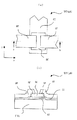
図1は、前記p型薄膜トランジスタTFT(pD)の一実施例を示す構成図で、(a)は平面図を、(b)は(a)のb−b線における断面図を示している。
図2は、本発明による表示装置の基板上に、前記p型薄膜トランジスタTFT(pD)とともに、n型薄膜トランジスタTFT(nD)を形成した、たとえばコンプリメンタリ型薄膜トランジスタの構成を示す断面図である。
図4(a)ないし(e)は、図2に示したn型薄膜トランジスタTFT(nD)とp型薄膜トランジスタTFT(pD)の製造方法の一実施例を示した工程図である。以下、工程順に説明する。
たとえばガラスからなる基板SUB1の表面には、ゲート電極GT'およびゲート電極GTを形成し、これらゲート電極GT'およびゲート電極GTをも被って絶縁膜GIを形成する。
前記半導体層ASに、脱水素処理を行った後、選択的に、パルスあるいは連続発振レーザを照射し、n型薄膜トランジスタTFT(nD)の形成領域およびp型薄膜トランジスタTFT(pD)の形成領域における前記半導体層ASの結晶化を行い、ポリSiからなる半導体層PSを形成する。この場合、前記半導体層ASの結晶化は全面に施すようにしてもよい。
前記半導体層ASをフォトリソグラフィ技術による選択エッチングをすることにより、n型薄膜トランジスタTFT(nD)の形成領域およびp型薄膜トランジスタTFT(pD)の形成領域に、それぞれ、ポリSiからなる半導体層PSを残存させる。
基板SUB1の表面の全域に、たとえばCVD(Chemical Vapor Deposition)を用い、たとえばリン(P)がドープされた半導体層(n(+)型半導体層)を厚さ10〜50nmで形成する。
基板SUB1の表面の全域に、たとえばスパッタリングによって、アルミニウム(Al)を膜厚300〜500nmで成膜する。
図5は、本発明による表示装置の他の実施例を示す構成図で、図2と対応した図となっている。図5において、図2と同符号のものは同材料で、同機能を有するようになっている。
図7(a)ないし(f)は、本発明による表示装置の製造方法の他の実施例を示す工程図である。
たとえばガラスからなる基板SUB1の表面に、ゲート電極GT'、ゲート電極GT、およびゲート電極GT"を形成し、これらゲート電極GT'、ゲート電極GT、およびゲート電極GT"をも被って絶縁膜GIを形成する。
前記半導体層ASに、脱水素処理を行った後に、選択的に、パルスあるいは連続発振レーザを照射し、n型薄膜トランジスタTFT(nD)の形成領域およびp型薄膜トランジスタTFT(pD)の形成領域における前記半導体層ASの結晶化を行い、ポリSiからなる半導体層PSを形成する。この場合、前記半導体層ASの結晶化は全面に施すようにしてもよい。
前記半導体層ASをフォトリソグラフィ技術による選択エッチングをすることにより、n型薄膜トランジスタTFT(nD)の形成領域およびp型薄膜トランジスタTFT(pD)の形成領域に、それぞれ、ポリSiからなる半導体層PSを残存させる。
前記基板SUB1の表面に、たとえばCVD(Chemical Vapor Deposition)を用いて、アモルファスSiからなる半導体層AS'を膜厚50〜250nmで形成し、この半導体層AS'をフォトリソグラフィ技術による選択エッチングをすることにより、n型薄膜トランジスタTFT(nD)、p型薄膜トランジスタTFT(pD)、およびn型薄膜トランジスタTFT(nP)の各形成領域に残存させる。
基板SUB1の表面の全域に、たとえばCVD(Chemical Vapor Deposition)を用い、たとえばリン(P)がドープされた半導体層(n(+)型半導体層)を厚さ10〜50nmで形成する。
基板SUB1の表面の全域に、たとえばスパッタリングによって、アルミニウム(Al)を膜厚300〜500nmで成膜する。
Claims (6)
- 基板上にp型薄膜トランジスタを備える表示装置であって、
前記p型薄膜トランジスタは、
ゲート電極の上面に絶縁膜を介して半導体層が形成され、
前記半導体層の上面に離間部を有して互いに対向配置され、アルミニュウム、ガリウム、インジウム、タリウムのうちのいずれかの材料を主材料とするドレイン電極とソース電極とが形成され、
前記ドレイン電極と前記半導体層の界面、および前記ソース電極と前記半導体層の界面に、p型不純物の拡散層が形成されて構成されており、
前記p型不純物の拡散層は、前記ドレイン電極と前記ソース電極を構成する主材料が前記半導体層に拡散して形成されていることを特徴とする表示装置。 - 基板上にp型薄膜トランジスタおよびn型薄膜トランジスタを備える表示装置であって、
これら各薄膜トランジスタは、ゲート電極の上面に絶縁膜を介して半導体層が形成され、前記半導体層の上面に離間部を有して互いに対向配置され、アルミニュウム、ガリウム、インジウム、タリウムのうちのいずれかの材料を主材料とするドレイン電極とソース電極とが形成されて構成され、
前記p型薄膜トランジスタは、前記ドレイン電極と前記半導体層の界面、および前記ソース電極と前記半導体層の界面に、p型不純物の拡散層が形成され、前記p型不純物の拡散層は、前記ドレイン電極と前記ソース電極を構成する主材料が前記半導体層に拡散して形成されており、
前記n型薄膜トランジスタは、前記ドレイン電極と前記半導体層の界面、および前記ソース電極と前記半導体層の界面に、n型不純物がドープされた半導体層が介在されていることを特徴とする表示装置。 - 基板上にp型薄膜トランジスタおよびn型薄膜トランジスタを備える表示装置であって、
これら各薄膜トランジスタは、ゲート電極の上面に絶縁膜を介して半導体層が形成され、前記半導体層の上面に離間部を有して互いに対向配置され、アルミニュウム、ガリウム、インジウム、タリウムのうちのいずれかの材料を主材料とするドレイン電極とソース電極とが形成されて構成され、
前記p型薄膜トランジスタは、前記ドレイン電極と前記半導体層の界面、および前記ソース電極と前記半導体層の界面に、p型不純物の拡散層が形成され、前記p型不純物の拡散層は、前記ドレイン電極と前記ソース電極を構成する主材料が前記半導体層に拡散して形成されており、
前記n型薄膜トランジスタは、前記ドレイン電極と前記半導体層の界面、および前記ソース電極と前記半導体層の界面に、n型不純物がドープされた半導体層および前記ドレイン電極とソース電極の材料の前記半導体層への拡散を防止する拡散バリア層の順次積層体が介在されていることを特徴とする表示装置。 - 前記半導体層は、多結晶半導体層で形成されていることを特徴とする請求項1に記載の表示装置。
- 前記半導体層は、多結晶半導体層と非晶質半導体層の順次積層体から構成されていることを特徴とする請求項1に記載の表示装置。
- 基板上にp型薄膜トランジスタを備え、該p型薄膜トランジスタは、ゲート電極の上面に絶縁膜を介して半導体層が形成され、前記半導体層の上面に離間部を有して互いに対向配置され、アルミニュウム、ガリウム、インジウム、タリウムのうちのいずれかの材料を主材料とするドレイン電極とソース電極とが形成されて構成される表示装置の製造方法であって、
アニールを施すことによって、前記ドレイン電極と前記半導体層の界面、および前記ソース電極と前記半導体層の界面に、前記ドレイン電極と前記ソース電極を構成する主材料が前記半導体層に拡散して形成されるp型不純物の拡散層を形成することを特徴とする表示装置の製造方法。
Priority Applications (6)
| Application Number | Priority Date | Filing Date | Title |
|---|---|---|---|
| JP2008049885A JP5363009B2 (ja) | 2008-02-29 | 2008-02-29 | 表示装置およびその製造方法 |
| CN2009100057992A CN101521210B (zh) | 2008-02-29 | 2009-02-12 | 显示装置及其制造方法 |
| TW098105315A TWI401805B (zh) | 2008-02-29 | 2009-02-19 | 顯示裝置 |
| KR1020090016353A KR101043115B1 (ko) | 2008-02-29 | 2009-02-26 | 표시 장치 및 그 제조 방법 |
| US12/379,662 US8058654B2 (en) | 2008-02-29 | 2009-02-26 | Display device and manufacturing method thereof |
| EP09153984.1A EP2096673B1 (en) | 2008-02-29 | 2009-02-27 | Method of manufacturing display device |
Applications Claiming Priority (1)
| Application Number | Priority Date | Filing Date | Title |
|---|---|---|---|
| JP2008049885A JP5363009B2 (ja) | 2008-02-29 | 2008-02-29 | 表示装置およびその製造方法 |
Publications (3)
| Publication Number | Publication Date |
|---|---|
| JP2009206437A JP2009206437A (ja) | 2009-09-10 |
| JP2009206437A5 JP2009206437A5 (ja) | 2011-02-10 |
| JP5363009B2 true JP5363009B2 (ja) | 2013-12-11 |
Family
ID=40719637
Family Applications (1)
| Application Number | Title | Priority Date | Filing Date |
|---|---|---|---|
| JP2008049885A Active JP5363009B2 (ja) | 2008-02-29 | 2008-02-29 | 表示装置およびその製造方法 |
Country Status (6)
| Country | Link |
|---|---|
| US (1) | US8058654B2 (ja) |
| EP (1) | EP2096673B1 (ja) |
| JP (1) | JP5363009B2 (ja) |
| KR (1) | KR101043115B1 (ja) |
| CN (1) | CN101521210B (ja) |
| TW (1) | TWI401805B (ja) |
Families Citing this family (7)
| Publication number | Priority date | Publication date | Assignee | Title |
|---|---|---|---|---|
| JP5111167B2 (ja) * | 2008-03-06 | 2012-12-26 | 株式会社ジャパンディスプレイイースト | 液晶表示装置 |
| FR2944140B1 (fr) * | 2009-04-02 | 2011-09-16 | Commissariat Energie Atomique | Dispositif de detection d'image electronique |
| KR20110081694A (ko) * | 2010-01-08 | 2011-07-14 | 삼성모바일디스플레이주식회사 | 박막 트랜지스터의 제조 방법 및 표시 장치의 제조 방법 |
| JP5708910B2 (ja) * | 2010-03-30 | 2015-04-30 | ソニー株式会社 | 薄膜トランジスタおよびその製造方法、並びに表示装置 |
| TWI666776B (zh) | 2014-06-20 | 2019-07-21 | 日商半導體能源研究所股份有限公司 | 半導體裝置以及包括該半導體裝置的顯示裝置 |
| JP6544166B2 (ja) * | 2015-09-14 | 2019-07-17 | 信越化学工業株式会社 | SiC複合基板の製造方法 |
| CN105470310A (zh) | 2016-01-21 | 2016-04-06 | 京东方科技集团股份有限公司 | 一种薄膜晶体管及其制作方法、阵列基板和显示装置 |
Family Cites Families (22)
| Publication number | Priority date | Publication date | Assignee | Title |
|---|---|---|---|---|
| GB2044994B (en) | 1979-03-22 | 1983-06-15 | Philips Electronic Associated | Thin film transistors |
| JPH0693509B2 (ja) | 1983-08-26 | 1994-11-16 | シャープ株式会社 | 薄膜トランジスタ |
| ATE77177T1 (de) | 1985-10-04 | 1992-06-15 | Hosiden Corp | Duennfilmtransistor und verfahren zu seiner herstellung. |
| JPH0563196A (ja) * | 1991-09-04 | 1993-03-12 | Hitachi Ltd | 薄膜半導体装置及びその製造方法並び液晶表示装置 |
| JPH06188265A (ja) | 1992-12-22 | 1994-07-08 | Matsushita Electric Ind Co Ltd | 半導体装置およびその製造方法 |
| JPH08204032A (ja) * | 1995-01-20 | 1996-08-09 | Mitsubishi Electric Corp | 半導体装置及びその製造方法 |
| JP3516424B2 (ja) * | 1996-03-10 | 2004-04-05 | 株式会社半導体エネルギー研究所 | 薄膜半導体装置 |
| JP2757850B2 (ja) | 1996-04-18 | 1998-05-25 | 日本電気株式会社 | 薄膜トランジスタおよびその製造方法 |
| JP4019461B2 (ja) * | 1996-09-06 | 2007-12-12 | セイコーエプソン株式会社 | カラー表示装置とその製造方法およびカラー液晶装置 |
| US6620719B1 (en) * | 2000-03-31 | 2003-09-16 | International Business Machines Corporation | Method of forming ohmic contacts using a self doping layer for thin-film transistors |
| JP2002202527A (ja) * | 2000-12-28 | 2002-07-19 | Nec Corp | アクティブマトリクス型液晶表示装置 |
| JP2004079735A (ja) | 2002-08-15 | 2004-03-11 | Nec Corp | 薄膜トランジスタの製造方法 |
| TW554539B (en) * | 2002-09-09 | 2003-09-21 | Chunghwa Picture Tubes Ltd | Thin film transistor source/drain structure and manufacturing method thereof |
| KR100904266B1 (ko) | 2002-12-31 | 2009-06-25 | 엘지디스플레이 주식회사 | 박막 트랜지스터 어레이 기판의 제조 방법 |
| JP4316896B2 (ja) | 2003-01-09 | 2009-08-19 | 株式会社 日立ディスプレイズ | 表示装置とその製造方法 |
| KR100584715B1 (ko) * | 2004-04-06 | 2006-05-29 | 엘지.필립스 엘시디 주식회사 | 구동회로 일체형 액정표시장치용 어레이 기판의 제조 방법 |
| JP5036173B2 (ja) * | 2004-11-26 | 2012-09-26 | 株式会社半導体エネルギー研究所 | 半導体装置の作製方法 |
| US20060138403A1 (en) * | 2004-12-29 | 2006-06-29 | Gang Yu | Organic electronic devices including pixels |
| US7521710B2 (en) * | 2006-02-16 | 2009-04-21 | Idemitsu Kosan Co., Ltd. | Organic thin film transistor |
| US7646015B2 (en) * | 2006-10-31 | 2010-01-12 | Semiconductor Energy Laboratory Co., Ltd. | Manufacturing method of semiconductor device and semiconductor device |
| JP5303119B2 (ja) * | 2007-06-05 | 2013-10-02 | 株式会社ジャパンディスプレイ | 半導体装置 |
| JP2008311545A (ja) * | 2007-06-18 | 2008-12-25 | Hitachi Displays Ltd | 表示装置 |
-
2008
- 2008-02-29 JP JP2008049885A patent/JP5363009B2/ja active Active
-
2009
- 2009-02-12 CN CN2009100057992A patent/CN101521210B/zh active Active
- 2009-02-19 TW TW098105315A patent/TWI401805B/zh active
- 2009-02-26 KR KR1020090016353A patent/KR101043115B1/ko active IP Right Grant
- 2009-02-26 US US12/379,662 patent/US8058654B2/en active Active
- 2009-02-27 EP EP09153984.1A patent/EP2096673B1/en active Active
Also Published As
| Publication number | Publication date |
|---|---|
| KR101043115B1 (ko) | 2011-06-20 |
| EP2096673A3 (en) | 2011-04-20 |
| CN101521210B (zh) | 2012-05-23 |
| US20090218575A1 (en) | 2009-09-03 |
| TW201001711A (en) | 2010-01-01 |
| TWI401805B (zh) | 2013-07-11 |
| KR20090093849A (ko) | 2009-09-02 |
| JP2009206437A (ja) | 2009-09-10 |
| US8058654B2 (en) | 2011-11-15 |
| CN101521210A (zh) | 2009-09-02 |
| EP2096673A2 (en) | 2009-09-02 |
| EP2096673B1 (en) | 2021-06-02 |
Similar Documents
| Publication | Publication Date | Title |
|---|---|---|
| JP2010003910A (ja) | 表示素子 | |
| KR100990818B1 (ko) | 표시 장치 및 표시 장치의 제조 방법 | |
| JP5363009B2 (ja) | 表示装置およびその製造方法 | |
| JP5384088B2 (ja) | 表示装置 | |
| JP2008041865A (ja) | 表示装置及びその製造方法 | |
| US7642141B2 (en) | Manufacturing method for display device | |
| US8129724B2 (en) | Display device including first, second, and third semiconductor films | |
| TWI447916B (zh) | 顯示裝置 | |
| US20080296583A1 (en) | Display Device And Manufacturing Method of The Same | |
| JP4984369B2 (ja) | 画像表示装置及びその製造方法 | |
| US7173675B2 (en) | LCD display with contact hole and insulation layer above pixel electrode | |
| JP5346477B2 (ja) | 表示装置およびその製造方法 | |
| JP2008311545A (ja) | 表示装置 | |
| JP2004253520A (ja) | 表示装置とその製造方法 | |
| KR20080047773A (ko) | 폴리실리콘 박막 트랜지스터 기판 및 그 제조 방법 | |
| JPH06169086A (ja) | 多結晶シリコン薄膜トランジスタ | |
| TWI459566B (zh) | 薄膜電晶體、具有其之顯示裝置及製造薄膜電晶體與顯示裝置之方法 | |
| JPH10209452A (ja) | 薄膜トランジスタ及びその製造方法 | |
| JP2010205850A (ja) | 表示装置 | |
| JP2009021276A (ja) | 薄膜トランジスタ、表示装置、及び薄膜トランジスタの製造方法 | |
| US20120217502A1 (en) | Display device and manufacturing method of the same | |
| JPH09139505A (ja) | 薄膜半導体装置 | |
| JP2009070862A (ja) | 表示装置およびその製造方法 | |
| JP2004006974A (ja) | アクティブマトリクス回路の作製方法 | |
| JP2008021803A (ja) | 薄膜トランジスタ |
Legal Events
| Date | Code | Title | Description |
|---|---|---|---|
| A521 | Request for written amendment filed |
Free format text: JAPANESE INTERMEDIATE CODE: A523 Effective date: 20101207 |
|
| A621 | Written request for application examination |
Free format text: JAPANESE INTERMEDIATE CODE: A621 Effective date: 20101207 |
|
| A521 | Request for written amendment filed |
Free format text: JAPANESE INTERMEDIATE CODE: A523 Effective date: 20101216 |
|
| A711 | Notification of change in applicant |
Free format text: JAPANESE INTERMEDIATE CODE: A712 Effective date: 20110218 |
|
| RD03 | Notification of appointment of power of attorney |
Free format text: JAPANESE INTERMEDIATE CODE: A7423 Effective date: 20110218 |
|
| A977 | Report on retrieval |
Free format text: JAPANESE INTERMEDIATE CODE: A971007 Effective date: 20130116 |
|
| A131 | Notification of reasons for refusal |
Free format text: JAPANESE INTERMEDIATE CODE: A131 Effective date: 20130122 |
|
| A521 | Request for written amendment filed |
Free format text: JAPANESE INTERMEDIATE CODE: A523 Effective date: 20130319 |
|
| TRDD | Decision of grant or rejection written | ||
| A01 | Written decision to grant a patent or to grant a registration (utility model) |
Free format text: JAPANESE INTERMEDIATE CODE: A01 Effective date: 20130827 |
|
| A61 | First payment of annual fees (during grant procedure) |
Free format text: JAPANESE INTERMEDIATE CODE: A61 Effective date: 20130905 |
|
| R150 | Certificate of patent or registration of utility model |
Ref document number: 5363009 Country of ref document: JP Free format text: JAPANESE INTERMEDIATE CODE: R150 Free format text: JAPANESE INTERMEDIATE CODE: R150 |
|
| R250 | Receipt of annual fees |
Free format text: JAPANESE INTERMEDIATE CODE: R250 |
|
| R250 | Receipt of annual fees |
Free format text: JAPANESE INTERMEDIATE CODE: R250 |
|
| R250 | Receipt of annual fees |
Free format text: JAPANESE INTERMEDIATE CODE: R250 |
|
| R250 | Receipt of annual fees |
Free format text: JAPANESE INTERMEDIATE CODE: R250 |
|
| R250 | Receipt of annual fees |
Free format text: JAPANESE INTERMEDIATE CODE: R250 |
|
| R250 | Receipt of annual fees |
Free format text: JAPANESE INTERMEDIATE CODE: R250 |
|
| R250 | Receipt of annual fees |
Free format text: JAPANESE INTERMEDIATE CODE: R250 |
|
| S111 | Request for change of ownership or part of ownership |
Free format text: JAPANESE INTERMEDIATE CODE: R313117 |
|
| R250 | Receipt of annual fees |
Free format text: JAPANESE INTERMEDIATE CODE: R250 |
|
| R350 | Written notification of registration of transfer |
Free format text: JAPANESE INTERMEDIATE CODE: R350 |