JP5326558B2 - 半導体装置の製造方法 - Google Patents
半導体装置の製造方法 Download PDFInfo
- Publication number
- JP5326558B2 JP5326558B2 JP2008332602A JP2008332602A JP5326558B2 JP 5326558 B2 JP5326558 B2 JP 5326558B2 JP 2008332602 A JP2008332602 A JP 2008332602A JP 2008332602 A JP2008332602 A JP 2008332602A JP 5326558 B2 JP5326558 B2 JP 5326558B2
- Authority
- JP
- Japan
- Prior art keywords
- insulating film
- polishing
- film
- dielectric constant
- organic insulating
- Prior art date
- Legal status (The legal status is an assumption and is not a legal conclusion. Google has not performed a legal analysis and makes no representation as to the accuracy of the status listed.)
- Expired - Fee Related
Links
Images


Classifications
-
- H—ELECTRICITY
- H01—ELECTRIC ELEMENTS
- H01L—SEMICONDUCTOR DEVICES NOT COVERED BY CLASS H10
- H01L21/00—Processes or apparatus adapted for the manufacture or treatment of semiconductor or solid state devices or of parts thereof
- H01L21/70—Manufacture or treatment of devices consisting of a plurality of solid state components formed in or on a common substrate or of parts thereof; Manufacture of integrated circuit devices or of parts thereof
- H01L21/71—Manufacture of specific parts of devices defined in group H01L21/70
- H01L21/768—Applying interconnections to be used for carrying current between separate components within a device comprising conductors and dielectrics
- H01L21/76801—Applying interconnections to be used for carrying current between separate components within a device comprising conductors and dielectrics characterised by the formation and the after-treatment of the dielectrics, e.g. smoothing
- H01L21/76822—Modification of the material of dielectric layers, e.g. grading, after-treatment to improve the stability of the layers, to increase their density etc.
- H01L21/76825—Modification of the material of dielectric layers, e.g. grading, after-treatment to improve the stability of the layers, to increase their density etc. by exposing the layer to particle radiation, e.g. ion implantation, irradiation with UV light or electrons etc.
-
- H—ELECTRICITY
- H01—ELECTRIC ELEMENTS
- H01L—SEMICONDUCTOR DEVICES NOT COVERED BY CLASS H10
- H01L21/00—Processes or apparatus adapted for the manufacture or treatment of semiconductor or solid state devices or of parts thereof
- H01L21/02—Manufacture or treatment of semiconductor devices or of parts thereof
- H01L21/02104—Forming layers
- H01L21/02107—Forming insulating materials on a substrate
- H01L21/02109—Forming insulating materials on a substrate characterised by the type of layer, e.g. type of material, porous/non-porous, pre-cursors, mixtures or laminates
- H01L21/02112—Forming insulating materials on a substrate characterised by the type of layer, e.g. type of material, porous/non-porous, pre-cursors, mixtures or laminates characterised by the material of the layer
- H01L21/02123—Forming insulating materials on a substrate characterised by the type of layer, e.g. type of material, porous/non-porous, pre-cursors, mixtures or laminates characterised by the material of the layer the material containing silicon
-
- H—ELECTRICITY
- H01—ELECTRIC ELEMENTS
- H01L—SEMICONDUCTOR DEVICES NOT COVERED BY CLASS H10
- H01L21/00—Processes or apparatus adapted for the manufacture or treatment of semiconductor or solid state devices or of parts thereof
- H01L21/02—Manufacture or treatment of semiconductor devices or of parts thereof
- H01L21/02104—Forming layers
- H01L21/02107—Forming insulating materials on a substrate
- H01L21/02109—Forming insulating materials on a substrate characterised by the type of layer, e.g. type of material, porous/non-porous, pre-cursors, mixtures or laminates
- H01L21/02205—Forming insulating materials on a substrate characterised by the type of layer, e.g. type of material, porous/non-porous, pre-cursors, mixtures or laminates the layer being characterised by the precursor material for deposition
- H01L21/02208—Forming insulating materials on a substrate characterised by the type of layer, e.g. type of material, porous/non-porous, pre-cursors, mixtures or laminates the layer being characterised by the precursor material for deposition the precursor containing a compound comprising Si
- H01L21/02211—Forming insulating materials on a substrate characterised by the type of layer, e.g. type of material, porous/non-porous, pre-cursors, mixtures or laminates the layer being characterised by the precursor material for deposition the precursor containing a compound comprising Si the compound being a silane, e.g. disilane, methylsilane or chlorosilane
-
- H—ELECTRICITY
- H01—ELECTRIC ELEMENTS
- H01L—SEMICONDUCTOR DEVICES NOT COVERED BY CLASS H10
- H01L21/00—Processes or apparatus adapted for the manufacture or treatment of semiconductor or solid state devices or of parts thereof
- H01L21/02—Manufacture or treatment of semiconductor devices or of parts thereof
- H01L21/02104—Forming layers
- H01L21/02107—Forming insulating materials on a substrate
- H01L21/02109—Forming insulating materials on a substrate characterised by the type of layer, e.g. type of material, porous/non-porous, pre-cursors, mixtures or laminates
- H01L21/02205—Forming insulating materials on a substrate characterised by the type of layer, e.g. type of material, porous/non-porous, pre-cursors, mixtures or laminates the layer being characterised by the precursor material for deposition
- H01L21/02208—Forming insulating materials on a substrate characterised by the type of layer, e.g. type of material, porous/non-porous, pre-cursors, mixtures or laminates the layer being characterised by the precursor material for deposition the precursor containing a compound comprising Si
- H01L21/02214—Forming insulating materials on a substrate characterised by the type of layer, e.g. type of material, porous/non-porous, pre-cursors, mixtures or laminates the layer being characterised by the precursor material for deposition the precursor containing a compound comprising Si the compound comprising silicon and oxygen
- H01L21/02216—Forming insulating materials on a substrate characterised by the type of layer, e.g. type of material, porous/non-porous, pre-cursors, mixtures or laminates the layer being characterised by the precursor material for deposition the precursor containing a compound comprising Si the compound comprising silicon and oxygen the compound being a molecule comprising at least one silicon-oxygen bond and the compound having hydrogen or an organic group attached to the silicon or oxygen, e.g. a siloxane
-
- H—ELECTRICITY
- H01—ELECTRIC ELEMENTS
- H01L—SEMICONDUCTOR DEVICES NOT COVERED BY CLASS H10
- H01L21/00—Processes or apparatus adapted for the manufacture or treatment of semiconductor or solid state devices or of parts thereof
- H01L21/02—Manufacture or treatment of semiconductor devices or of parts thereof
- H01L21/02104—Forming layers
- H01L21/02107—Forming insulating materials on a substrate
- H01L21/02225—Forming insulating materials on a substrate characterised by the process for the formation of the insulating layer
- H01L21/0226—Forming insulating materials on a substrate characterised by the process for the formation of the insulating layer formation by a deposition process
- H01L21/02282—Forming insulating materials on a substrate characterised by the process for the formation of the insulating layer formation by a deposition process liquid deposition, e.g. spin-coating, sol-gel techniques, spray coating
-
- H—ELECTRICITY
- H01—ELECTRIC ELEMENTS
- H01L—SEMICONDUCTOR DEVICES NOT COVERED BY CLASS H10
- H01L21/00—Processes or apparatus adapted for the manufacture or treatment of semiconductor or solid state devices or of parts thereof
- H01L21/02—Manufacture or treatment of semiconductor devices or of parts thereof
- H01L21/02104—Forming layers
- H01L21/02107—Forming insulating materials on a substrate
- H01L21/02296—Forming insulating materials on a substrate characterised by the treatment performed before or after the formation of the layer
- H01L21/02318—Forming insulating materials on a substrate characterised by the treatment performed before or after the formation of the layer post-treatment
- H01L21/02345—Forming insulating materials on a substrate characterised by the treatment performed before or after the formation of the layer post-treatment treatment by exposure to radiation, e.g. visible light
- H01L21/02351—Forming insulating materials on a substrate characterised by the treatment performed before or after the formation of the layer post-treatment treatment by exposure to radiation, e.g. visible light treatment by exposure to corpuscular radiation, e.g. exposure to electrons, alpha-particles, protons or ions
-
- H—ELECTRICITY
- H01—ELECTRIC ELEMENTS
- H01L—SEMICONDUCTOR DEVICES NOT COVERED BY CLASS H10
- H01L21/00—Processes or apparatus adapted for the manufacture or treatment of semiconductor or solid state devices or of parts thereof
- H01L21/02—Manufacture or treatment of semiconductor devices or of parts thereof
- H01L21/04—Manufacture or treatment of semiconductor devices or of parts thereof the devices having potential barriers, e.g. a PN junction, depletion layer or carrier concentration layer
- H01L21/18—Manufacture or treatment of semiconductor devices or of parts thereof the devices having potential barriers, e.g. a PN junction, depletion layer or carrier concentration layer the devices having semiconductor bodies comprising elements of Group IV of the Periodic Table or AIIIBV compounds with or without impurities, e.g. doping materials
- H01L21/30—Treatment of semiconductor bodies using processes or apparatus not provided for in groups H01L21/20 - H01L21/26
- H01L21/31—Treatment of semiconductor bodies using processes or apparatus not provided for in groups H01L21/20 - H01L21/26 to form insulating layers thereon, e.g. for masking or by using photolithographic techniques; After treatment of these layers; Selection of materials for these layers
- H01L21/3105—After-treatment
- H01L21/31051—Planarisation of the insulating layers
- H01L21/31053—Planarisation of the insulating layers involving a dielectric removal step
-
- H—ELECTRICITY
- H01—ELECTRIC ELEMENTS
- H01L—SEMICONDUCTOR DEVICES NOT COVERED BY CLASS H10
- H01L21/00—Processes or apparatus adapted for the manufacture or treatment of semiconductor or solid state devices or of parts thereof
- H01L21/02—Manufacture or treatment of semiconductor devices or of parts thereof
- H01L21/04—Manufacture or treatment of semiconductor devices or of parts thereof the devices having potential barriers, e.g. a PN junction, depletion layer or carrier concentration layer
- H01L21/18—Manufacture or treatment of semiconductor devices or of parts thereof the devices having potential barriers, e.g. a PN junction, depletion layer or carrier concentration layer the devices having semiconductor bodies comprising elements of Group IV of the Periodic Table or AIIIBV compounds with or without impurities, e.g. doping materials
- H01L21/30—Treatment of semiconductor bodies using processes or apparatus not provided for in groups H01L21/20 - H01L21/26
- H01L21/31—Treatment of semiconductor bodies using processes or apparatus not provided for in groups H01L21/20 - H01L21/26 to form insulating layers thereon, e.g. for masking or by using photolithographic techniques; After treatment of these layers; Selection of materials for these layers
- H01L21/3205—Deposition of non-insulating-, e.g. conductive- or resistive-, layers on insulating layers; After-treatment of these layers
- H01L21/321—After treatment
- H01L21/32115—Planarisation
- H01L21/3212—Planarisation by chemical mechanical polishing [CMP]
-
- H—ELECTRICITY
- H01—ELECTRIC ELEMENTS
- H01L—SEMICONDUCTOR DEVICES NOT COVERED BY CLASS H10
- H01L21/00—Processes or apparatus adapted for the manufacture or treatment of semiconductor or solid state devices or of parts thereof
- H01L21/70—Manufacture or treatment of devices consisting of a plurality of solid state components formed in or on a common substrate or of parts thereof; Manufacture of integrated circuit devices or of parts thereof
- H01L21/71—Manufacture of specific parts of devices defined in group H01L21/70
- H01L21/768—Applying interconnections to be used for carrying current between separate components within a device comprising conductors and dielectrics
- H01L21/76801—Applying interconnections to be used for carrying current between separate components within a device comprising conductors and dielectrics characterised by the formation and the after-treatment of the dielectrics, e.g. smoothing
- H01L21/76819—Smoothing of the dielectric
-
- H—ELECTRICITY
- H01—ELECTRIC ELEMENTS
- H01L—SEMICONDUCTOR DEVICES NOT COVERED BY CLASS H10
- H01L21/00—Processes or apparatus adapted for the manufacture or treatment of semiconductor or solid state devices or of parts thereof
- H01L21/70—Manufacture or treatment of devices consisting of a plurality of solid state components formed in or on a common substrate or of parts thereof; Manufacture of integrated circuit devices or of parts thereof
- H01L21/71—Manufacture of specific parts of devices defined in group H01L21/70
- H01L21/768—Applying interconnections to be used for carrying current between separate components within a device comprising conductors and dielectrics
- H01L21/76801—Applying interconnections to be used for carrying current between separate components within a device comprising conductors and dielectrics characterised by the formation and the after-treatment of the dielectrics, e.g. smoothing
- H01L21/76835—Combinations of two or more different dielectric layers having a low dielectric constant
-
- H—ELECTRICITY
- H01—ELECTRIC ELEMENTS
- H01L—SEMICONDUCTOR DEVICES NOT COVERED BY CLASS H10
- H01L21/00—Processes or apparatus adapted for the manufacture or treatment of semiconductor or solid state devices or of parts thereof
- H01L21/70—Manufacture or treatment of devices consisting of a plurality of solid state components formed in or on a common substrate or of parts thereof; Manufacture of integrated circuit devices or of parts thereof
- H01L21/71—Manufacture of specific parts of devices defined in group H01L21/70
- H01L21/768—Applying interconnections to be used for carrying current between separate components within a device comprising conductors and dielectrics
- H01L21/76838—Applying interconnections to be used for carrying current between separate components within a device comprising conductors and dielectrics characterised by the formation and the after-treatment of the conductors
- H01L21/7684—Smoothing; Planarisation
-
- H—ELECTRICITY
- H01—ELECTRIC ELEMENTS
- H01L—SEMICONDUCTOR DEVICES NOT COVERED BY CLASS H10
- H01L23/00—Details of semiconductor or other solid state devices
- H01L23/52—Arrangements for conducting electric current within the device in operation from one component to another, i.e. interconnections, e.g. wires, lead frames
- H01L23/522—Arrangements for conducting electric current within the device in operation from one component to another, i.e. interconnections, e.g. wires, lead frames including external interconnections consisting of a multilayer structure of conductive and insulating layers inseparably formed on the semiconductor body
- H01L23/532—Arrangements for conducting electric current within the device in operation from one component to another, i.e. interconnections, e.g. wires, lead frames including external interconnections consisting of a multilayer structure of conductive and insulating layers inseparably formed on the semiconductor body characterised by the materials
- H01L23/5329—Insulating materials
- H01L23/53295—Stacked insulating layers
-
- H—ELECTRICITY
- H01—ELECTRIC ELEMENTS
- H01L—SEMICONDUCTOR DEVICES NOT COVERED BY CLASS H10
- H01L2924/00—Indexing scheme for arrangements or methods for connecting or disconnecting semiconductor or solid-state bodies as covered by H01L24/00
- H01L2924/0001—Technical content checked by a classifier
- H01L2924/0002—Not covered by any one of groups H01L24/00, H01L24/00 and H01L2224/00
-
- H—ELECTRICITY
- H01—ELECTRIC ELEMENTS
- H01L—SEMICONDUCTOR DEVICES NOT COVERED BY CLASS H10
- H01L2924/00—Indexing scheme for arrangements or methods for connecting or disconnecting semiconductor or solid-state bodies as covered by H01L24/00
- H01L2924/10—Details of semiconductor or other solid state devices to be connected
- H01L2924/11—Device type
- H01L2924/12—Passive devices, e.g. 2 terminal devices
- H01L2924/1204—Optical Diode
- H01L2924/12044—OLED
Landscapes
- Engineering & Computer Science (AREA)
- Physics & Mathematics (AREA)
- Condensed Matter Physics & Semiconductors (AREA)
- General Physics & Mathematics (AREA)
- Computer Hardware Design (AREA)
- Microelectronics & Electronic Packaging (AREA)
- Power Engineering (AREA)
- Manufacturing & Machinery (AREA)
- Spectroscopy & Molecular Physics (AREA)
- Plasma & Fusion (AREA)
- Internal Circuitry In Semiconductor Integrated Circuit Devices (AREA)
- Formation Of Insulating Films (AREA)
Description
ここで、近年では、多層配線の微細化が進むにつれて、配線材料の抵抗により生じる動作遅延が問題となってきた。このような動作遅延への対策としては、配線材料として抵抗値がアルミニウムよりも低い銅や、銅合金を用いることがあげられる。一方、マスクとドライエッチング法を用いる製造方法では配線をより微細化することが難しくなっているため、化学機械研磨(CMP)法を用いたダマシン法を採用して配線を微細化することが行われている。
そこで、従来では、低誘電率膜上にキャップ膜として例えば誘電率4.2の酸化膜(SiO2)を形成した後に配線形成と研磨を行っていた。このようなキャップ膜は、低誘電率膜よりも研磨スラリに対する濡れ性が良好なので、絶縁膜の研磨が進行し、ディッシングを抑制できる。さらに膜強度が高く、密着性も高いので、研磨時の膜剥がれを防止できる。なお、膜剥がれの防止などの観点から、研磨工程ではキャップ層を一定の膜厚で残していた。
これに対する対応策としては、キャップ膜を設けずに、低圧力研磨により低誘電率膜を直接研磨する方法が考えられるが、低圧力研磨では研磨レートが低く、生産時のタクトの悪化や、研磨剤の使用量増加によるコストの増大の原因となる。さらに、低圧力研磨を用いた場合でも、低誘電率膜の疎水性によるスラリの濡れ性の悪化は解消できなかった。
本発明は、このような事情を鑑みてなされたものであり、絶縁膜の寄生容量を低減させる構成において、配線の微細化させた半導体装置を効率よく製造できるようにすることを主な目的とする。
で電子ビームを照射し、前記有機絶縁膜の前記メチル基の少なくとも一部をヒドロキシ基に置換する工程と、前記電子ビームを照射した後、前記有機絶縁膜に溝を形成する工程と、前記有機絶縁膜上及び前記溝内にバリアメタル膜を形成する工程と、前記バリアメタル膜の上方にめっき層を形成する工程と、前記有機絶縁膜上の前記めっき層を第1の研磨砥液を用いた研磨により除去し、更に前記有機絶縁膜上の前記バリアメタル膜及び前記有機絶縁膜の表面を第2の研磨砥液を用いて研磨する工程と、を有し、前記電子ビームを照射した前記有機絶縁膜の表面の第2の研磨砥液を用いた研磨レートは、前記電子ビーム照射前の前記有機絶縁膜の前記第2の研磨砥液を用いた研磨レートより速いことを特徴とする半導体装置の製造方法が提供される。
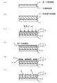
まず、図1(a)に示すように、半導体基板1上に、化学気相成長(CVD)法により第1の絶縁膜2を例えば、10nm〜200nmの膜厚に堆積させる。半導体基板1としては、例えばシリコン基板を使用する。また、図示を省略するが、第1の絶縁膜2の下層には、トランジスタや金属配線やコンタクトプラグが形成される。この工程で第1の絶縁膜2は、後述するエッチング工程でストッパー膜として機能するもので、例えば、炭化シリコン素膜(SiC)や、炭窒化シリコン膜(SiCN)、窒化シリコン膜(SiN)が採用される。第1の絶縁膜2は、薄膜を2層以上積層させた構造でも良い。さらに、これらの膜に、酸化膜(SiO)や、炭化シリコン酸化膜(SiOC)等と組み合わせても良い。
最初に、第1の絶縁膜2の表面にスピンコート法を用いて塗布用薬液を塗布する。塗布用薬液としては、例えば、触媒化成社製のNCS(Nano Crystaline Silica)があげられる。半導体基板1の回転数は、1000rpm〜5000rpmとする。この後、半導体基板1を例えば150℃〜300℃の温度雰囲気で、3分〜10分ベーキングして溶媒を蒸発させる。さらに、半導体基板1を拡散炉に搬入し、400℃の温度雰囲気中で30分間加熱し、架橋反応のためのキュア処理を行う。
また、CVD法に好適な低誘電率絶縁膜としては、AMAT社製のBlack Diamond(商品名)、ASM社製のAurora(商品名)、ノベラス社製のCORAL(商品名)などがあげられる。
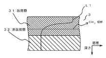
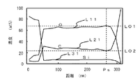
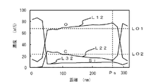
図7は、改質前、即ち電子ビーム照射を行う前の測定結果を示す。横軸は低誘電率絶縁膜3の膜厚方向の距離を示し、縦軸は膜中の酸素と炭素とSiの濃度を示す。ラインL11は酸素濃度を示し、ラインL21は炭素濃度を、ラインL31はSi濃度をそれぞれ示している。また、横軸のPsは、低誘電率絶縁膜3の表面付近を示している。電子ビーム照射を行う前は、ラインL11に示す酸素濃度、及びラインL21に示す炭素濃度は、深さによらず略一定(ラインLO1,LO2参照)であった。
まず、表面改質後の低誘電率絶縁膜3上に、エッチングのハードマスクとなる第2の絶縁膜4をCVD法やPE−CVD法やPVD法により厚さ10nm〜150nmに堆積させる。第2の絶縁膜4としては、例えば、二酸化シリコン膜(SiO2)や、炭化シリコン膜(SiC)、炭酸化シリコン膜(SiOC)、炭窒化シリコン膜(SiCN)、窒化シリコン膜(SiN)のような絶縁膜又は、金属膜などが挙げられる。また、これらの膜を単層、或いは2層以上積層して用いても良い。なお、エッチングやCMP法による加工性を考慮すると、第2の絶縁膜4は二酸化シリコン膜(SiO2)であることが望ましい。
即ち、第2の絶縁膜4上にフォトレジストを塗布し、露光及び現像を行って配線溝の配置に合わせた開口を有するレジストパターン5を形成する。さらに、レジストパターン5をマスクにして、第2の絶縁膜4をRIE(Reactive Ion Etching)によりエッチングし、第2の絶縁膜4に配線溝の形状を転写する。これにより、第2の絶縁膜4からなるハードマスク4aが形成される。
第2の絶縁膜4を用いて形成されたハードマスク4aを用いて、低誘電率絶縁膜3をエッチングし、低誘電率絶縁膜3に配線溝となる溝パターン6を形成する。エッチングは、各絶縁膜2〜4に対して個別にエッチングガスを切り替えることにより行われる。
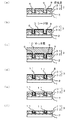
絶縁膜3,4に対しては、CF4ガスが使用される。ここで、CF4ガスに対する低誘電率絶縁膜3と第1の絶縁膜2との選択比は比較的に大きい。このため、低誘電率絶縁膜3のエッチングは、第1の絶縁膜2でストップする。なお、第1の絶縁膜2をエッチングする場合、CF4ガスとO2ガスとの混合ガスが使用される。
低誘電率絶縁膜3の最表面及び溝パターン6の内面を覆うように、バリアメタル膜となる導電膜8をPVD法、例えばスパッタ法で1nm〜30nmの厚さに堆積させる。この導電膜8は、配線材料に用いるCuが低誘電率絶縁膜3中に拡散することを防止するために堆積され、例えば窒化タンタル(TaN)が用いられる。堆積条件は、例えば、N2ガスとArガスをN2 :Ar=20:80の流量比で流し、Taターゲットに例えば1kW〜40kWの電力を投入する。これにより、TaとN2ガスとを反応させる。
導電膜8上に、Cuからなるシード膜9をPVD法、例えばスパッタ法により膜厚1nm〜100nmに堆積させる。この場合、Arガス雰囲気中でCuターゲットに例えば1kW〜40kWの電力を投入する。成膜方法は、PVD法の他に、CVD法、ALD法、PE−CVD法、ALD法、PE−ALD法であっても良い。
ここでは、シード膜9を給電部として使用し、シード膜9上に配線材料となるCuを析出させ、配線材料で溝パターン6を埋める。めっき層10の厚さは、低誘電率絶縁膜3の膜厚以上、例えば1.2μmとする。これにより、溝パターン6にCuが埋め込まれると共に、低誘電率絶縁膜3の表面上にもCuが所定の厚さで析出する。
ここでの研磨工程には、例えばロータリ式研磨法を用いることができる。図9及び図10は研磨装置の一例を示す。なお、図中の矢印は回転の向き,或いは機構の動作範囲を示す。
研磨パッド22上には、半導体基板1を保持する研磨ヘッド23が配置されている。研磨ヘッド23は、半導体基板1を被研磨面、即ちめっき層10が下向きになるように保持する。さらに、研磨ヘッド23には、図示を省略する押圧機構が設けられており、半導体基板1を研磨パッド22に押し付けることができる。
なお、ここでの研磨条件は、例えば、ワークテーブル21の回転数を70rpmとし、研磨ヘッド23の回転数を71rpmとした。研磨圧力は、例えば1.4000×10⁴Pa(2.0psi)とする。
なお、アルカリ系の研磨砥液を使用することも可能である。ただし、アルカリ系の研磨砥液は、スラリは馴染み易くなるが、脆弱な低誘電率絶縁膜3に対する研磨レートが過度に高くなるのでコントロールが困難になる。このため、低誘電率絶縁膜3上に保護膜を形成することを目的とした、アニオン系、カチオン系、ノニオン系、非イオン系の中の1種又はそれ以上の界面活性剤や改質剤を含有させた研磨砥液を用いることが好ましい。
図2(d)に示すように、最初に、配線材料からなるめっき層10とシード膜9とが第1の研磨により除去される。次に、図2(e)に示すように、導電膜8が第2の研磨により除去される。これにより、低誘電率絶縁膜3の最表面、即ち改質層31が露出する。さらに、図2(f)に示すように、第3の研磨を行い、低誘電率絶縁膜3の改質層31の少なくとも一部を配線材料と共に除去する。これにより、低誘電率絶縁膜3に配線となる導電性パターン11が形成される。なお、低誘電率絶縁膜3は、改質層31を全て除去し、非改質部32のみを残しても良い。
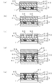
まず、図3(a)に示すように、低誘電率絶縁膜3上に、誘電率が3.0以下の層間絶縁膜41と、エッチングのストッパー膜として機能する第3の絶縁膜42と、誘電率が3.0以下の低誘電率絶縁膜43とを順番に形成する。層間絶縁膜41と低誘電率絶縁膜43の材料及び形成方法は、前記の低誘電率絶縁膜3と同様である。また、第3の絶縁膜42の材料及び形成方法は、第1の絶縁膜2と同様である。
さらに、図3(c)に示すように、ハードマスクを使用したドライエッチングを行い、低誘電率絶縁膜53に配線用の溝パターン56を形成する。このときのエッチングでは、第3の絶縁膜42がストッパーとして働くので、溝パターン56が層間絶縁膜41にまで形成されることはない。
なお、3層目以降にも同様の工程を繰り返すことで、ディッシングを抑制しながらより多層の配線構造を実現できる。
また、このようにして製造された半導体装置は、絶縁膜の寄生容量を低減でき、配線の微細化を実現することができる。
(付記1)半導体基板の上方に有機絶縁膜を形成する工程と、前記有機絶縁膜の表面に電子ビームを照射する工程と、前記有機絶縁膜に溝を形成する工程と、前記有機絶縁膜上及び前記溝内に導電材を形成する工程と、前記有機絶縁膜上の前記導電材を研磨により除去し、前記有機絶縁膜の表面を露出させる工程と、を有することを特徴とする半導体装置の製造方法。
(付記2)前記有機絶縁膜の誘電率が3.0以下であることを特徴とする付記1に記載の半導体装置の製造方法。
(付記3)前記有機絶縁膜は、メチル基を含む材料から形成されていることを特徴とする請求項1に記載の半導体装置の製造方法。
(付記4)前記有機絶縁膜は、メチル基を含む材料から形成されていることを特徴とする付記1乃至付記3のいずれか一項に記載の半導体装置の製造方法。
(付記5)電子ビームの照射により、前記有機絶縁膜の前記メチル基の少なくとも一部をヒドロキシ基に置換することを特徴とする付記1又は付記2に記載の半導体装置の製造方法。
(付記6)前記有機絶縁膜は、メチルシラン、ジメチルシラン、トリメチルシラン、テトラメチルシラン、フェニルシラン、メチルフェニルシラン、シクロヘキシルシラン、エチルシラン、ジエチルシラン、テトラエトキシシラン、ジメチルジエトキシシラン、ジメチルジメトキシシラン、ジメチルエトキシシラン、メチルジエトキシシラン、トリエトキシシラン、トリメチルフェノキシシラン、フェノキシシラン、ジエトキシシラン、ジアセトキシメチルシラン、メチルトリエトキシシラン、ジ−tert−ブチルシラン、tert−ブチルシラン、ジ−tert−ブチルシラン、1,3,5,7−テトラメチルシクロテトラシロキサン、オクタメチルシクロテトラシロキサン、ヘキサメチルシクロトリシロキサン、ヘキサメチルジシロキサン、1,1,2,2−テトラメチルジシロキサン、オクタメチルトリシロキサンのいずれか1つまたはその組み合わせからなる材料を用いて形成されていることを特徴とする請求項3又は請求項4に記載の半導体装置の製造方法。
(付記7)研磨で使用するスラリは、フュームドシリカ、セリウム、アルミナ、炭化珪素の少なくとも1つを含む砥粒と、水酸化カリウム又はアンモニウムからなる分散剤と、過硫酸アンモニウム又は過酸化水素水酸化剤からなる酸化剤と、ベンゾトリアゾール(BTA)からなる防食剤、クエン酸又はリンゴ酸からなるキレート剤と、を含むことを特徴とする付記1乃至付記6のいずれか一項に記載の半導体装置の製造方法。
(付記8)電子ビームの照射条件は、加速電圧が2keV〜4keV、照射量が50μC/cm2〜400μC/cm2、処理温度が200℃〜500℃であることを特徴とする付記1乃至付記6のいずれか一項に記載の半導体装置の製造方法。
(付記9)電子ビームを照射した前記有機絶縁膜上にマスク用の絶縁膜を形成し、前記マスク用の絶縁膜をパターニングしてから前記有機絶縁膜をエッチングして前記溝を形成した後、前記マスク用の絶縁膜を研磨により除去することを特徴とする付記1乃至付記8のいずれか一項に記載の半導体装置の製造方法。
(付記10)半導体基板と、前記半導体基板の上方に形成され、第一の層と、前記第一の層上に設けられ、前記第一の層のメチル基の少なくとも一部をヒドロキシ基に置換して形成された第二の層とからなる有機絶縁膜と、前記有機絶縁膜の溝内に埋め込まれた導電材と、を有することを特徴とする半導体装置。
(付記11)前記有機絶縁膜の誘電率が3.0以下であることを特徴とする付記10に記載の半導体装置。
(付記12)前記有機絶縁膜の前記第二の層は、膜厚方向に前記メチル基の濃度勾配を有し、最表面の前記メチル基の濃度が最も低いことを特徴とする付記10又は付記11に記載の半導体装置。
2 第1の絶縁膜
3 低誘電率絶縁膜(有機絶縁膜)
4 第2の絶縁膜
5 レジストパターン
6 パターン
8 バリアメタル膜
9 シード層
10 めっき層
11 導電性パターン
31 改質層(第二の層)
32 非改質層(第一の層)
Claims (2)
- 半導体基板の上方にメチル基を含む誘電率が3.0以下の有機絶縁膜を形成する工程と、
前記有機絶縁膜の表面に、加速電圧が2keV〜4keV、照射量が50μC/cm2〜400μC/cm2、処理温度が200℃〜500℃の条件で電子ビームを照射し、前記有機絶縁膜の前記メチル基の少なくとも一部をヒドロキシ基に置換する工程と、
前記電子ビームを照射した後、前記有機絶縁膜に溝を形成する工程と、
前記有機絶縁膜上及び前記溝内にバリアメタル膜を形成する工程と、
前記バリアメタル膜の上方にめっき層を形成する工程と、
前記有機絶縁膜上の前記めっき層を第1の研磨砥液を用いた研磨により除去し、更に前記有機絶縁膜上の前記バリアメタル膜及び前記有機絶縁膜の表面を第2の研磨砥液を用いて研磨する工程と、
を有し、
前記電子ビームを照射した前記有機絶縁膜の表面の第2の研磨砥液を用いた研磨レートは、前記電子ビーム照射前の前記有機絶縁膜の前記第2の研磨砥液を用いた研磨レートより速いことを特徴とする半導体装置の製造方法。 - 前記第2の研磨砥液は、前記第1の研磨砥液と異なることを特徴とする請求項1に記載の半導体装置の製造方法。
Priority Applications (2)
| Application Number | Priority Date | Filing Date | Title |
|---|---|---|---|
| JP2008332602A JP5326558B2 (ja) | 2008-12-26 | 2008-12-26 | 半導体装置の製造方法 |
| US12/603,207 US8026164B2 (en) | 2008-12-26 | 2009-10-21 | Semiconductor device and method of manufacturing the same |
Applications Claiming Priority (1)
| Application Number | Priority Date | Filing Date | Title |
|---|---|---|---|
| JP2008332602A JP5326558B2 (ja) | 2008-12-26 | 2008-12-26 | 半導体装置の製造方法 |
Publications (2)
| Publication Number | Publication Date |
|---|---|
| JP2010153723A JP2010153723A (ja) | 2010-07-08 |
| JP5326558B2 true JP5326558B2 (ja) | 2013-10-30 |
Family
ID=42283906
Family Applications (1)
| Application Number | Title | Priority Date | Filing Date |
|---|---|---|---|
| JP2008332602A Expired - Fee Related JP5326558B2 (ja) | 2008-12-26 | 2008-12-26 | 半導体装置の製造方法 |
Country Status (2)
| Country | Link |
|---|---|
| US (1) | US8026164B2 (ja) |
| JP (1) | JP5326558B2 (ja) |
Families Citing this family (12)
| Publication number | Priority date | Publication date | Assignee | Title |
|---|---|---|---|---|
| TWI480977B (zh) * | 2007-04-09 | 2015-04-11 | 哈佛大學校長及評議會 | 銅內連線用的氮化鈷層及其製造方法 |
| JP5343417B2 (ja) * | 2008-06-25 | 2013-11-13 | 富士通セミコンダクター株式会社 | 半導体装置およびその製造方法 |
| JP5487748B2 (ja) * | 2009-06-16 | 2014-05-07 | 東京エレクトロン株式会社 | バリヤ層、成膜方法及び処理システム |
| CN102543845B (zh) * | 2010-12-29 | 2014-10-22 | 中芯国际集成电路制造(北京)有限公司 | 半导体器件及其制作方法 |
| US8461683B2 (en) * | 2011-04-01 | 2013-06-11 | Intel Corporation | Self-forming, self-aligned barriers for back-end interconnects and methods of making same |
| US9376594B2 (en) * | 2012-03-16 | 2016-06-28 | Fujimi Incorporated | Polishing composition |
| US9492910B2 (en) * | 2012-07-25 | 2016-11-15 | Ebara Corporation | Polishing method |
| JP6049340B2 (ja) | 2012-07-25 | 2016-12-21 | 株式会社荏原製作所 | 研磨フィルムの製造方法、研磨フィルム |
| US9514983B2 (en) * | 2012-12-28 | 2016-12-06 | Intel Corporation | Cobalt based interconnects and methods of fabrication thereof |
| US9997457B2 (en) * | 2013-12-20 | 2018-06-12 | Intel Corporation | Cobalt based interconnects and methods of fabrication thereof |
| US11233008B2 (en) * | 2019-06-19 | 2022-01-25 | Samsung Electronics Co., Ltd. | Method of manufacturing an integrated circuit with buried power rail |
| CN112436027B (zh) * | 2020-11-23 | 2024-07-23 | 长江先进存储产业创新中心有限责任公司 | 半导体结构及其制造方法 |
Family Cites Families (6)
| Publication number | Priority date | Publication date | Assignee | Title |
|---|---|---|---|---|
| JPH0429149A (ja) * | 1990-05-24 | 1992-01-31 | Matsushita Electric Ind Co Ltd | パターン形成材料およびパターン形成方法 |
| US6761975B1 (en) * | 1999-12-23 | 2004-07-13 | Honeywell International Inc. | Polycarbosilane adhesion promoters for low dielectric constant polymeric materials |
| US7384693B2 (en) * | 2004-04-28 | 2008-06-10 | Intel Corporation | Diamond-like carbon films with low dielectric constant and high mechanical strength |
| JP2006156519A (ja) | 2004-11-26 | 2006-06-15 | Renesas Technology Corp | 半導体装置の製造方法 |
| JP2008053402A (ja) * | 2006-08-24 | 2008-03-06 | Sony Corp | 半導体装置の製造方法 |
| JP2009117743A (ja) * | 2007-11-09 | 2009-05-28 | Panasonic Corp | 半導体装置及びその製造方法 |
-
2008
- 2008-12-26 JP JP2008332602A patent/JP5326558B2/ja not_active Expired - Fee Related
-
2009
- 2009-10-21 US US12/603,207 patent/US8026164B2/en not_active Expired - Fee Related
Also Published As
| Publication number | Publication date |
|---|---|
| JP2010153723A (ja) | 2010-07-08 |
| US20100164119A1 (en) | 2010-07-01 |
| US8026164B2 (en) | 2011-09-27 |
Similar Documents
| Publication | Publication Date | Title |
|---|---|---|
| JP5326558B2 (ja) | 半導体装置の製造方法 | |
| US6713873B1 (en) | Adhesion between dielectric materials | |
| CN101431046B (zh) | 在用于减少rc延迟的介电层中产生气隙的方法和装置 | |
| KR100359552B1 (ko) | 반도체 기판의 표면 평탄화 처리 방법 및 절연층에서의 전도성 플러그 생성 방법 | |
| KR100810788B1 (ko) | 듀얼 다마신 구조의 에칭 방법 | |
| US7795142B2 (en) | Method for fabricating a semiconductor device | |
| TWI528454B (zh) | 半導體裝置及半導體裝置之製造方法 | |
| US8614146B2 (en) | Semiconductor device manufacture method and semiconductor device | |
| US6841466B1 (en) | Method of selectively making copper using plating technology | |
| JP2008117903A (ja) | 半導体装置の製造方法 | |
| KR20010098409A (ko) | 저 비유전율층 보호 방법과 상호 접속 구조체 형성 방법및 벌크 유전체 물질이 보호되는 중간 반도체 디바이스와상호 접속 구조를 갖는 반도체 기판 구조체 | |
| JP4160569B2 (ja) | 半導体装置の製造方法 | |
| US6717265B1 (en) | Treatment of low-k dielectric material for CMP | |
| WO2007091574A1 (ja) | 多層配線構造および多層配線の製造方法 | |
| WO2010084535A1 (ja) | 半導体装置およびその製造方法 | |
| JP5823359B2 (ja) | 半導体装置の製造方法 | |
| JP2006294815A (ja) | 半導体装置及びその製造方法 | |
| US20090191706A1 (en) | Method for fabricating a semiconductor device | |
| JP5861346B2 (ja) | 半導体装置の製造方法 | |
| JP2001284355A (ja) | 半導体装置およびその製造方法 | |
| JP2006156519A (ja) | 半導体装置の製造方法 | |
| JP2005340604A (ja) | 半導体装置の製造方法 | |
| JP4499487B2 (ja) | 半導体装置の製造方法 | |
| JP2011155074A (ja) | 半導体装置の製造方法 | |
| JP2006525651A (ja) | low−k誘電体の最上部に反射防止特性を持つキャップ層の形成法 |
Legal Events
| Date | Code | Title | Description |
|---|---|---|---|
| A621 | Written request for application examination |
Free format text: JAPANESE INTERMEDIATE CODE: A621 Effective date: 20110822 |
|
| A977 | Report on retrieval |
Free format text: JAPANESE INTERMEDIATE CODE: A971007 Effective date: 20120308 |
|
| A131 | Notification of reasons for refusal |
Free format text: JAPANESE INTERMEDIATE CODE: A131 Effective date: 20120313 |
|
| A521 | Request for written amendment filed |
Free format text: JAPANESE INTERMEDIATE CODE: A523 Effective date: 20120514 |
|
| A02 | Decision of refusal |
Free format text: JAPANESE INTERMEDIATE CODE: A02 Effective date: 20120724 |
|
| A521 | Request for written amendment filed |
Free format text: JAPANESE INTERMEDIATE CODE: A523 Effective date: 20121024 |
|
| A911 | Transfer to examiner for re-examination before appeal (zenchi) |
Free format text: JAPANESE INTERMEDIATE CODE: A911 Effective date: 20121109 |
|
| A131 | Notification of reasons for refusal |
Free format text: JAPANESE INTERMEDIATE CODE: A131 Effective date: 20130115 |
|
| A521 | Request for written amendment filed |
Free format text: JAPANESE INTERMEDIATE CODE: A523 Effective date: 20130318 |
|
| TRDD | Decision of grant or rejection written | ||
| A01 | Written decision to grant a patent or to grant a registration (utility model) |
Free format text: JAPANESE INTERMEDIATE CODE: A01 Effective date: 20130625 |
|
| A61 | First payment of annual fees (during grant procedure) |
Free format text: JAPANESE INTERMEDIATE CODE: A61 Effective date: 20130708 |
|
| R150 | Certificate of patent or registration of utility model |
Ref document number: 5326558 Country of ref document: JP Free format text: JAPANESE INTERMEDIATE CODE: R150 Free format text: JAPANESE INTERMEDIATE CODE: R150 |
|
| S531 | Written request for registration of change of domicile |
Free format text: JAPANESE INTERMEDIATE CODE: R313531 |
|
| R350 | Written notification of registration of transfer |
Free format text: JAPANESE INTERMEDIATE CODE: R350 |
|
| S111 | Request for change of ownership or part of ownership |
Free format text: JAPANESE INTERMEDIATE CODE: R313111 |
|
| R350 | Written notification of registration of transfer |
Free format text: JAPANESE INTERMEDIATE CODE: R350 |
|
| LAPS | Cancellation because of no payment of annual fees |