JP5227525B2 - 生体光計測装置 - Google Patents
生体光計測装置 Download PDFInfo
- Publication number
- JP5227525B2 JP5227525B2 JP2007076844A JP2007076844A JP5227525B2 JP 5227525 B2 JP5227525 B2 JP 5227525B2 JP 2007076844 A JP2007076844 A JP 2007076844A JP 2007076844 A JP2007076844 A JP 2007076844A JP 5227525 B2 JP5227525 B2 JP 5227525B2
- Authority
- JP
- Japan
- Prior art keywords
- light
- wavelength
- layer
- light emitting
- biological
- Prior art date
- Legal status (The legal status is an assumption and is not a legal conclusion. Google has not performed a legal analysis and makes no representation as to the accuracy of the status listed.)
- Expired - Fee Related
Links
Images


Classifications
-
- G—PHYSICS
- G01—MEASURING; TESTING
- G01N—INVESTIGATING OR ANALYSING MATERIALS BY DETERMINING THEIR CHEMICAL OR PHYSICAL PROPERTIES
- G01N21/00—Investigating or analysing materials by the use of optical means, i.e. using sub-millimetre waves, infrared, visible or ultraviolet light
- G01N21/17—Systems in which incident light is modified in accordance with the properties of the material investigated
- G01N21/25—Colour; Spectral properties, i.e. comparison of effect of material on the light at two or more different wavelengths or wavelength bands
- G01N21/31—Investigating relative effect of material at wavelengths characteristic of specific elements or molecules, e.g. atomic absorption spectrometry
- G01N21/314—Investigating relative effect of material at wavelengths characteristic of specific elements or molecules, e.g. atomic absorption spectrometry with comparison of measurements at specific and non-specific wavelengths
- G01N21/3151—Investigating relative effect of material at wavelengths characteristic of specific elements or molecules, e.g. atomic absorption spectrometry with comparison of measurements at specific and non-specific wavelengths using two sources of radiation of different wavelengths
-
- A—HUMAN NECESSITIES
- A61—MEDICAL OR VETERINARY SCIENCE; HYGIENE
- A61B—DIAGNOSIS; SURGERY; IDENTIFICATION
- A61B5/00—Measuring for diagnostic purposes; Identification of persons
- A61B5/145—Measuring characteristics of blood in vivo, e.g. gas concentration, pH value; Measuring characteristics of body fluids or tissues, e.g. interstitial fluid, cerebral tissue
- A61B5/1455—Measuring characteristics of blood in vivo, e.g. gas concentration, pH value; Measuring characteristics of body fluids or tissues, e.g. interstitial fluid, cerebral tissue using optical sensors, e.g. spectral photometrical oximeters
- A61B5/14551—Measuring characteristics of blood in vivo, e.g. gas concentration, pH value; Measuring characteristics of body fluids or tissues, e.g. interstitial fluid, cerebral tissue using optical sensors, e.g. spectral photometrical oximeters for measuring blood gases
- A61B5/14552—Details of sensors specially adapted therefor
-
- B—PERFORMING OPERATIONS; TRANSPORTING
- B82—NANOTECHNOLOGY
- B82Y—SPECIFIC USES OR APPLICATIONS OF NANOSTRUCTURES; MEASUREMENT OR ANALYSIS OF NANOSTRUCTURES; MANUFACTURE OR TREATMENT OF NANOSTRUCTURES
- B82Y20/00—Nanooptics, e.g. quantum optics or photonic crystals
-
- A—HUMAN NECESSITIES
- A61—MEDICAL OR VETERINARY SCIENCE; HYGIENE
- A61B—DIAGNOSIS; SURGERY; IDENTIFICATION
- A61B2562/00—Details of sensors; Constructional details of sensor housings or probes; Accessories for sensors
- A61B2562/02—Details of sensors specially adapted for in-vivo measurements
- A61B2562/0233—Special features of optical sensors or probes classified in A61B5/00
-
- A—HUMAN NECESSITIES
- A61—MEDICAL OR VETERINARY SCIENCE; HYGIENE
- A61B—DIAGNOSIS; SURGERY; IDENTIFICATION
- A61B2562/00—Details of sensors; Constructional details of sensor housings or probes; Accessories for sensors
- A61B2562/04—Arrangements of multiple sensors of the same type
- A61B2562/043—Arrangements of multiple sensors of the same type in a linear array
-
- A—HUMAN NECESSITIES
- A61—MEDICAL OR VETERINARY SCIENCE; HYGIENE
- A61B—DIAGNOSIS; SURGERY; IDENTIFICATION
- A61B2562/00—Details of sensors; Constructional details of sensor housings or probes; Accessories for sensors
- A61B2562/04—Arrangements of multiple sensors of the same type
- A61B2562/046—Arrangements of multiple sensors of the same type in a matrix array
-
- A—HUMAN NECESSITIES
- A61—MEDICAL OR VETERINARY SCIENCE; HYGIENE
- A61B—DIAGNOSIS; SURGERY; IDENTIFICATION
- A61B5/00—Measuring for diagnostic purposes; Identification of persons
- A61B5/0059—Measuring for diagnostic purposes; Identification of persons using light, e.g. diagnosis by transillumination, diascopy, fluorescence
-
- G—PHYSICS
- G01—MEASURING; TESTING
- G01N—INVESTIGATING OR ANALYSING MATERIALS BY DETERMINING THEIR CHEMICAL OR PHYSICAL PROPERTIES
- G01N21/00—Investigating or analysing materials by the use of optical means, i.e. using sub-millimetre waves, infrared, visible or ultraviolet light
- G01N21/17—Systems in which incident light is modified in accordance with the properties of the material investigated
- G01N21/25—Colour; Spectral properties, i.e. comparison of effect of material on the light at two or more different wavelengths or wavelength bands
- G01N21/31—Investigating relative effect of material at wavelengths characteristic of specific elements or molecules, e.g. atomic absorption spectrometry
- G01N21/314—Investigating relative effect of material at wavelengths characteristic of specific elements or molecules, e.g. atomic absorption spectrometry with comparison of measurements at specific and non-specific wavelengths
- G01N2021/3144—Investigating relative effect of material at wavelengths characteristic of specific elements or molecules, e.g. atomic absorption spectrometry with comparison of measurements at specific and non-specific wavelengths for oxymetry
-
- G—PHYSICS
- G01—MEASURING; TESTING
- G01N—INVESTIGATING OR ANALYSING MATERIALS BY DETERMINING THEIR CHEMICAL OR PHYSICAL PROPERTIES
- G01N21/00—Investigating or analysing materials by the use of optical means, i.e. using sub-millimetre waves, infrared, visible or ultraviolet light
- G01N21/17—Systems in which incident light is modified in accordance with the properties of the material investigated
- G01N21/25—Colour; Spectral properties, i.e. comparison of effect of material on the light at two or more different wavelengths or wavelength bands
- G01N21/31—Investigating relative effect of material at wavelengths characteristic of specific elements or molecules, e.g. atomic absorption spectrometry
- G01N21/314—Investigating relative effect of material at wavelengths characteristic of specific elements or molecules, e.g. atomic absorption spectrometry with comparison of measurements at specific and non-specific wavelengths
- G01N2021/3148—Investigating relative effect of material at wavelengths characteristic of specific elements or molecules, e.g. atomic absorption spectrometry with comparison of measurements at specific and non-specific wavelengths using three or more wavelengths
-
- H—ELECTRICITY
- H01—ELECTRIC ELEMENTS
- H01L—SEMICONDUCTOR DEVICES NOT COVERED BY CLASS H10
- H01L2224/00—Indexing scheme for arrangements for connecting or disconnecting semiconductor or solid-state bodies and methods related thereto as covered by H01L24/00
- H01L2224/01—Means for bonding being attached to, or being formed on, the surface to be connected, e.g. chip-to-package, die-attach, "first-level" interconnects; Manufacturing methods related thereto
- H01L2224/42—Wire connectors; Manufacturing methods related thereto
- H01L2224/47—Structure, shape, material or disposition of the wire connectors after the connecting process
- H01L2224/48—Structure, shape, material or disposition of the wire connectors after the connecting process of an individual wire connector
- H01L2224/481—Disposition
- H01L2224/48135—Connecting between different semiconductor or solid-state bodies, i.e. chip-to-chip
- H01L2224/48137—Connecting between different semiconductor or solid-state bodies, i.e. chip-to-chip the bodies being arranged next to each other, e.g. on a common substrate
-
- H—ELECTRICITY
- H01—ELECTRIC ELEMENTS
- H01S—DEVICES USING THE PROCESS OF LIGHT AMPLIFICATION BY STIMULATED EMISSION OF RADIATION [LASER] TO AMPLIFY OR GENERATE LIGHT; DEVICES USING STIMULATED EMISSION OF ELECTROMAGNETIC RADIATION IN WAVE RANGES OTHER THAN OPTICAL
- H01S5/00—Semiconductor lasers
- H01S5/02—Structural details or components not essential to laser action
- H01S5/022—Mountings; Housings
- H01S5/0225—Out-coupling of light
- H01S5/02257—Out-coupling of light using windows, e.g. specially adapted for back-reflecting light to a detector inside the housing
-
- H—ELECTRICITY
- H01—ELECTRIC ELEMENTS
- H01S—DEVICES USING THE PROCESS OF LIGHT AMPLIFICATION BY STIMULATED EMISSION OF RADIATION [LASER] TO AMPLIFY OR GENERATE LIGHT; DEVICES USING STIMULATED EMISSION OF ELECTROMAGNETIC RADIATION IN WAVE RANGES OTHER THAN OPTICAL
- H01S5/00—Semiconductor lasers
- H01S5/02—Structural details or components not essential to laser action
- H01S5/022—Mountings; Housings
- H01S5/0233—Mounting configuration of laser chips
- H01S5/0234—Up-side down mountings, e.g. Flip-chip, epi-side down mountings or junction down mountings
-
- H—ELECTRICITY
- H01—ELECTRIC ELEMENTS
- H01S—DEVICES USING THE PROCESS OF LIGHT AMPLIFICATION BY STIMULATED EMISSION OF RADIATION [LASER] TO AMPLIFY OR GENERATE LIGHT; DEVICES USING STIMULATED EMISSION OF ELECTROMAGNETIC RADIATION IN WAVE RANGES OTHER THAN OPTICAL
- H01S5/00—Semiconductor lasers
- H01S5/02—Structural details or components not essential to laser action
- H01S5/028—Coatings ; Treatment of the laser facets, e.g. etching, passivation layers or reflecting layers
- H01S5/0287—Facet reflectivity
-
- H—ELECTRICITY
- H01—ELECTRIC ELEMENTS
- H01S—DEVICES USING THE PROCESS OF LIGHT AMPLIFICATION BY STIMULATED EMISSION OF RADIATION [LASER] TO AMPLIFY OR GENERATE LIGHT; DEVICES USING STIMULATED EMISSION OF ELECTROMAGNETIC RADIATION IN WAVE RANGES OTHER THAN OPTICAL
- H01S5/00—Semiconductor lasers
- H01S5/06—Arrangements for controlling the laser output parameters, e.g. by operating on the active medium
- H01S5/068—Stabilisation of laser output parameters
- H01S5/0683—Stabilisation of laser output parameters by monitoring the optical output parameters
-
- H—ELECTRICITY
- H01—ELECTRIC ELEMENTS
- H01S—DEVICES USING THE PROCESS OF LIGHT AMPLIFICATION BY STIMULATED EMISSION OF RADIATION [LASER] TO AMPLIFY OR GENERATE LIGHT; DEVICES USING STIMULATED EMISSION OF ELECTROMAGNETIC RADIATION IN WAVE RANGES OTHER THAN OPTICAL
- H01S5/00—Semiconductor lasers
- H01S5/20—Structure or shape of the semiconductor body to guide the optical wave ; Confining structures perpendicular to the optical axis, e.g. index or gain guiding, stripe geometry, broad area lasers, gain tailoring, transverse or lateral reflectors, special cladding structures, MQW barrier reflection layers
- H01S5/22—Structure or shape of the semiconductor body to guide the optical wave ; Confining structures perpendicular to the optical axis, e.g. index or gain guiding, stripe geometry, broad area lasers, gain tailoring, transverse or lateral reflectors, special cladding structures, MQW barrier reflection layers having a ridge or stripe structure
-
- H—ELECTRICITY
- H01—ELECTRIC ELEMENTS
- H01S—DEVICES USING THE PROCESS OF LIGHT AMPLIFICATION BY STIMULATED EMISSION OF RADIATION [LASER] TO AMPLIFY OR GENERATE LIGHT; DEVICES USING STIMULATED EMISSION OF ELECTROMAGNETIC RADIATION IN WAVE RANGES OTHER THAN OPTICAL
- H01S5/00—Semiconductor lasers
- H01S5/30—Structure or shape of the active region; Materials used for the active region
- H01S5/32—Structure or shape of the active region; Materials used for the active region comprising PN junctions, e.g. hetero- or double- heterostructures
- H01S5/323—Structure or shape of the active region; Materials used for the active region comprising PN junctions, e.g. hetero- or double- heterostructures in AIIIBV compounds, e.g. AlGaAs-laser, InP-based laser
- H01S5/32308—Structure or shape of the active region; Materials used for the active region comprising PN junctions, e.g. hetero- or double- heterostructures in AIIIBV compounds, e.g. AlGaAs-laser, InP-based laser emitting light at a wavelength less than 900 nm
- H01S5/32333—Structure or shape of the active region; Materials used for the active region comprising PN junctions, e.g. hetero- or double- heterostructures in AIIIBV compounds, e.g. AlGaAs-laser, InP-based laser emitting light at a wavelength less than 900 nm based on InGaAsP
-
- H—ELECTRICITY
- H01—ELECTRIC ELEMENTS
- H01S—DEVICES USING THE PROCESS OF LIGHT AMPLIFICATION BY STIMULATED EMISSION OF RADIATION [LASER] TO AMPLIFY OR GENERATE LIGHT; DEVICES USING STIMULATED EMISSION OF ELECTROMAGNETIC RADIATION IN WAVE RANGES OTHER THAN OPTICAL
- H01S5/00—Semiconductor lasers
- H01S5/30—Structure or shape of the active region; Materials used for the active region
- H01S5/34—Structure or shape of the active region; Materials used for the active region comprising quantum well or superlattice structures, e.g. single quantum well [SQW] lasers, multiple quantum well [MQW] lasers or graded index separate confinement heterostructure [GRINSCH] lasers
- H01S5/3403—Structure or shape of the active region; Materials used for the active region comprising quantum well or superlattice structures, e.g. single quantum well [SQW] lasers, multiple quantum well [MQW] lasers or graded index separate confinement heterostructure [GRINSCH] lasers having a strained layer structure in which the strain performs a special function, e.g. general strain effects, strain versus polarisation
-
- H—ELECTRICITY
- H01—ELECTRIC ELEMENTS
- H01S—DEVICES USING THE PROCESS OF LIGHT AMPLIFICATION BY STIMULATED EMISSION OF RADIATION [LASER] TO AMPLIFY OR GENERATE LIGHT; DEVICES USING STIMULATED EMISSION OF ELECTROMAGNETIC RADIATION IN WAVE RANGES OTHER THAN OPTICAL
- H01S5/00—Semiconductor lasers
- H01S5/40—Arrangement of two or more semiconductor lasers, not provided for in groups H01S5/02 - H01S5/30
- H01S5/4025—Array arrangements, e.g. constituted by discrete laser diodes or laser bar
- H01S5/4031—Edge-emitting structures
- H01S5/4056—Edge-emitting structures emitting light in more than one direction
-
- H—ELECTRICITY
- H01—ELECTRIC ELEMENTS
- H01S—DEVICES USING THE PROCESS OF LIGHT AMPLIFICATION BY STIMULATED EMISSION OF RADIATION [LASER] TO AMPLIFY OR GENERATE LIGHT; DEVICES USING STIMULATED EMISSION OF ELECTROMAGNETIC RADIATION IN WAVE RANGES OTHER THAN OPTICAL
- H01S5/00—Semiconductor lasers
- H01S5/40—Arrangement of two or more semiconductor lasers, not provided for in groups H01S5/02 - H01S5/30
- H01S5/4025—Array arrangements, e.g. constituted by discrete laser diodes or laser bar
- H01S5/4087—Array arrangements, e.g. constituted by discrete laser diodes or laser bar emitting more than one wavelength
Landscapes
- Physics & Mathematics (AREA)
- Life Sciences & Earth Sciences (AREA)
- Health & Medical Sciences (AREA)
- Spectroscopy & Molecular Physics (AREA)
- Chemical & Material Sciences (AREA)
- Engineering & Computer Science (AREA)
- General Health & Medical Sciences (AREA)
- Biophysics (AREA)
- Optics & Photonics (AREA)
- Pathology (AREA)
- Nanotechnology (AREA)
- General Physics & Mathematics (AREA)
- Molecular Biology (AREA)
- Analytical Chemistry (AREA)
- Toxicology (AREA)
- Immunology (AREA)
- Crystallography & Structural Chemistry (AREA)
- Biomedical Technology (AREA)
- Heart & Thoracic Surgery (AREA)
- Medical Informatics (AREA)
- Biochemistry (AREA)
- Surgery (AREA)
- Animal Behavior & Ethology (AREA)
- Public Health (AREA)
- Veterinary Medicine (AREA)
- Investigating Or Analysing Materials By Optical Means (AREA)
- Semiconductor Lasers (AREA)
- Measurement Of The Respiration, Hearing Ability, Form, And Blood Characteristics Of Living Organisms (AREA)
Description
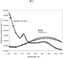
そこで、本発明は生体計測用の光源として、可視から赤外の複数の異なる波長で発振する半導体発光素子をひとつのカンパッケージに収納した小型光源装置およびその光源装置を搭載した生体光計測装置を提供することを目的とする。また、もうひとつには、生体計測用の光源として市場で入手困難であった700nm〜760nmの波長で発振する半導体レーザの特性安定化、高信頼化が可能となる構成を提案することを目的とする。
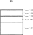
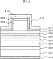
この波長範囲を満たすことのできる活性層として結晶成長方法が確立されていなかったために作製が困難であったGaAs基板上のInGaAsPを選ぶ。有機金属気層成長(MOVPE)装置を用いて、成長条件を実験的に最適化することでGaAs基板上にレーザの活性層相当の膜厚をもつInGaAsPを成長させることに成功した。成長条件はGaAs基板を用いた成長の常識的な範囲内のあるものであったが、装置ごとに最適化するべきものである。
なお、上記GaAs基板201は面方位が(100)面から<011>方向へ傾いたオフ基板でも良く、また、上記歪量子井戸活性層205は、障壁層に引張り歪を加えた歪補償構造でも良い。
特許文献1は生体の情報を得るために、光計測に先立ってCT計測が必要であるが、本発明では、光計測のみで生体情報を得る。特許文献2は光計測により生体情報を時系列表示できるが、その光源については波長以外の詳細な記述がない。本発明では特許文献2の信号処理理論をそのまま用いて、光計測装置に用いる光源の構成と光出力安定化の制御を提案した。
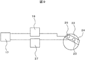
ここでは、生体計測の分光分析の精度を上げるために、半導体レーザ1〜3は、非常に近いが異なる周波数で変調されており、このときモニタ信号分離回路11としてはロックインアンプを用いるとよい。
これを第1の実施例の半導体レーザ2に適用することで生体光計測に適した光源を供給することができる。
1.格子定数aを有するGaAs基板上に設けられ、面内の格子定数awを有するIn1−xGaxAsyP1−y量子井戸層および障壁層からなる発光層を有し、前記発光層は、前記量子井戸層がε(%)=(aw−a)/a×100で定義される歪εが0.4%≦ε≦1.4%で、その組成が0.10≦y≦0.45であり、発光する波長が700nm以上760nm以下であることを特徴とする半導体レーザ装置。
2.格子定数aを有するGaAs基板上に設けられ、面内の格子定数awを有するIn1−xGaxAsyP1−y量子井戸層および障壁層からなる発光層を有し、前記発光層は、前記量子井戸層がε(%)=(aw−a)/a×100で定義される歪εが0.4%≦ε≦1.2%で、その組成が0.10≦y≦0.25であり、発光する波長が700nm以上730nm以下であることを特徴とする半導体レーザ装置。
3.格子定数aを有するGaAs基板上に設けられ、面内の格子定数awを有するIn1−xGaxAsyP1−y量子井戸層および障壁層からなる発光層を有し、前記発光層は、前記量子井戸層がε(%)=(aw−a)/a×100で定義される歪εが0.4%≦ε≦0.9%で、その組成が0.10≦y≦0.2であり、発光する波長が700nm以上720nm以下であることを特徴とする半導体レーザ装置。
4.格子定数aを有するGaAs基板上に設けられ、面内の格子定数awを有するIn1−xGaxAsyP1−y量子井戸層および障壁層からなる発光層を有し、前記発光層は、前記量子井戸層がε(%)=(aw−a)/a×100で定義される歪εが0.6%≦ε≦1.4%で、その組成が0.20≦y≦0.35であり、発光する波長が700nm以上760nm以下であることを特徴とする半導体レーザ装置。
5.格子定数aを有するGaAs基板上に設けられ、面内の格子定数awを有するIn1−xGaxAsyP1−y量子井戸層および障壁層からなる発光層を有し、前記発光層は、前記量子井戸層がε(%)=(aw−a)/a×100で定義される歪εが0.1%≦ε≦0.45%で、その組成が0.4≦y≦1.4であり、発光する波長が700nm以上760nm以下であることを特徴とする半導体レーザ装置。
6.格子定数aを有するGaAs基板上に設けられ、面内の格子定数awを有するIn1−xGaxAsyP1−y量子井戸層および障壁層からなる発光層を有し、前記発光層は、前記量子井戸層がε(%)=(aw−a)/a×100で定義される歪εが0.4%≦ε≦1.2%で、その組成が0.10≦y≦0.25であり、発光する波長が700nm以上730nm以下であることを特徴とする半導体レーザ装置。
7.所定のGaAs基板(格子定数a)上に設けられた、In1−xGaxAsyP1−y量子井戸層(面内の格子定数aw)および障壁層からなる発光層において、ε(%)=(aw−a)/a×100で定義される歪εが0.4%≦ε≦0.9%、量子井戸層の組成が0.10≦y≦0.20、波長が700nm以上720nm以下であることを特徴とする半導体発光装置を搭載したことを特徴とする半導体レーザ装置。
8.所定のGaAs基板(格子定数a)上に設けられた、In1−xGaxAsyP1−y量子井戸層(面内の格子定数aw)および障壁層からなる発光層において、ε(%)=(aw−a)/a×100で定義される歪εが0.6%≦ε≦1.4%、量子井戸層の組成が0.20≦y≦0.35、波長が725nm以上760nm以下であることを特徴とする半導体発光装置を搭載したことを特徴とする半導体レーザ装置。
Claims (10)
- 生体の表面に波長の互いに異なる複数の光信号を出射する光源装置と、
前記生体の内部を前記複数の光信号が通過して該生体の表面から放出される複数の光信号を検出する受光素子と、を備え、
前記光源装置は、サブマウント上に搭載され可視から赤外の波長範囲で互いに異なる波長を有する複数の半導体発光素子と、
前記複数の半導体発光素子に接続され光信号出力を制御して、異なる波長の光信号を放出させる駆動用回路と、
前記複数の半導体発光素子から放射される各々の光信号出力を検知する一つの光出力モニタ素子とが一つに収納されたパッケージを具備してなり、
前記一つの光出力モニタ素子で検出された複数の光信号を、該それぞれの波長を発する前記半導体発光素子に接続された前記駆動用回路の各々に帰還させることにより、前記複数の半導体発光素子の光信号出力の制御を行い、
前記パッケージはプローブに着脱可能な状態で固定され、
前記半導体発光素子の少なくとも一つが、格子定数aを有するGaAs基板上に設けられ、面内の格子定数a w を有するIn 1−x Ga x As y P 1−y 量子井戸層および障壁層からなる発光層を有し、
前記発光層は、前記量子井戸層がε(%)=(a w −a)/a×100で定義される歪εが0.4%≦ε≦1.4%で、その組成が0.10≦y≦0.45であり、発光する波長が700nm以上760nm以下であることを特徴とする生体光計測装置。 - 前記複数の光信号の波長の中で最も短い波長が、705±5nmであることを特徴とする請求項1記載の生体光計測装置。
- 前記複数の光信号のいずれかの光信号の波長が、755±5nmの範囲であることを特徴とする請求項1記載の生体光計測装置。
- 前記半導体発光素子から放射される光を拡げる手段を有することを特徴とする請求項1に記載の生体光計測装置。
- 前記半導体発光素子の光放出端面における、該光放出端面から放射される光の波長の反射率が、50%以上であることを特徴とする請求項1に記載の生体光計測装置。
- 前記半導体発光素子が、セルフパルセーション動作をすることを特徴とする請求項1に記載の生体光計測装置。
- 前記発光層は、前記量子井戸層がε(%)=(aw−a)/a×100で定義される歪εが0.4%≦ε≦1.2%で、その組成が0.10≦y≦0.25であり、発光する波長が700nm以上730nm以下であることを特徴とする請求項1に記載の生体光計測装置。
- 前記発光層は、前記量子井戸層がε(%)=(aw−a)/a×100で定義される歪εが0.4%≦ε≦0.9%で、その組成が0.10≦y≦0.2であり、発光する波長が700nm以上720nm以下であることを特徴とする請求項1に記載の生体光計測装置。
- 前記発光層は、前記量子井戸層がε(%)=(aw−a)/a×100で定義される歪εが0.6%≦ε≦1.4%で、その組成が0.20≦y≦0.35であり、発光する波長が725nm以上760nm以下であることを特徴とする請求項1に記載の生体光計測装置。
- 前記受光素子で検出された複数の光信号を受信し、該複数の光信号を波長ごとに分離する信号分離回路を備えていることを特徴とした、請求項1に記載の生体光計測装置。
Priority Applications (3)
| Application Number | Priority Date | Filing Date | Title |
|---|---|---|---|
| JP2007076844A JP5227525B2 (ja) | 2007-03-23 | 2007-03-23 | 生体光計測装置 |
| EP07021792.2A EP1972924B1 (en) | 2007-03-23 | 2007-11-09 | Light source comprising a plurality of semiconductor lasers mounted in one can and optical measurement instrument comprising such a light source |
| US11/984,279 US8369913B2 (en) | 2007-03-23 | 2007-11-15 | Optical measurement instrument for living body semiconductor laser installation for living body light measuring device |
Applications Claiming Priority (1)
| Application Number | Priority Date | Filing Date | Title |
|---|---|---|---|
| JP2007076844A JP5227525B2 (ja) | 2007-03-23 | 2007-03-23 | 生体光計測装置 |
Publications (3)
| Publication Number | Publication Date |
|---|---|
| JP2008229239A JP2008229239A (ja) | 2008-10-02 |
| JP2008229239A5 JP2008229239A5 (ja) | 2009-08-27 |
| JP5227525B2 true JP5227525B2 (ja) | 2013-07-03 |
Family
ID=39563139
Family Applications (1)
| Application Number | Title | Priority Date | Filing Date |
|---|---|---|---|
| JP2007076844A Expired - Fee Related JP5227525B2 (ja) | 2007-03-23 | 2007-03-23 | 生体光計測装置 |
Country Status (3)
| Country | Link |
|---|---|
| US (1) | US8369913B2 (ja) |
| EP (1) | EP1972924B1 (ja) |
| JP (1) | JP5227525B2 (ja) |
Families Citing this family (71)
| Publication number | Priority date | Publication date | Assignee | Title |
|---|---|---|---|---|
| WO2002036015A1 (en) | 2000-10-30 | 2002-05-10 | The General Hospital Corporation | Optical methods and systems for tissue analysis |
| EP1426411A1 (en) * | 2002-12-06 | 2004-06-09 | KRATON Polymers Research B.V. | Styrenic block copolymer compositions to be used for the manufacture of transparent, gel free films |
| CA2519937C (en) | 2003-03-31 | 2012-11-20 | Guillermo J. Tearney | Speckle reduction in optical coherence tomography by path length encoded angular compounding |
| EP2008579B1 (en) | 2003-06-06 | 2016-11-09 | The General Hospital Corporation | Process and apparatus for a wavelength tuned light source |
| WO2006014392A1 (en) | 2004-07-02 | 2006-02-09 | The General Hospital Corporation | Endoscopic imaging probe comprising dual clad fibre |
| ATE538714T1 (de) | 2004-08-24 | 2012-01-15 | Gen Hospital Corp | Verfahren, system und software-anordnung zur bestimmung des elastizitätsmoduls |
| WO2006024015A1 (en) | 2004-08-24 | 2006-03-02 | The General Hospital Corporation | Method and apparatus for imaging of vessel segments |
| EP1816949A1 (en) | 2004-11-29 | 2007-08-15 | The General Hospital Corporation | Arrangements, devices, endoscopes, catheters and methods for performing optical imaging by simultaneously illuminating and detecting multiple points on a sample |
| EP2085929A1 (en) | 2005-04-28 | 2009-08-05 | The General Hospital Corporation | Evaluating optical coherence tomography information for an anatomical structure |
| JP5702049B2 (ja) | 2005-06-01 | 2015-04-15 | ザ ジェネラル ホスピタル コーポレイション | 位相分解光学周波数領域画像化を行うための装置、方法及びシステム |
| EP2207008A1 (en) | 2005-08-09 | 2010-07-14 | The General Hospital Corporation | Apparatus and method for performing polarization-based quadrature demodulation in optical coherence tomography |
| EP1928306B1 (en) | 2005-09-29 | 2021-01-13 | General Hospital Corporation | Optical coherence tomography systems and methods including fluorescence microscopic imaging of one or more biological structures |
| US8145018B2 (en) | 2006-01-19 | 2012-03-27 | The General Hospital Corporation | Apparatus for obtaining information for a structure using spectrally-encoded endoscopy techniques and methods for producing one or more optical arrangements |
| EP2289398A3 (en) | 2006-01-19 | 2011-04-06 | The General Hospital Corporation | Methods and systems for optical imaging of epithelial luminal organs by beam scanning thereof |
| EP2659851A3 (en) | 2006-02-01 | 2014-01-15 | The General Hospital Corporation | Apparatus for applying a plurality of electro-magnetic radiations to a sample |
| JP5524487B2 (ja) | 2006-02-01 | 2014-06-18 | ザ ジェネラル ホスピタル コーポレイション | コンフォーマルレーザ治療手順を用いてサンプルの少なくとも一部分に電磁放射を放射する方法及びシステム。 |
| EP1987318B1 (en) | 2006-02-24 | 2015-08-12 | The General Hospital Corporation | Methods and systems for performing angle-resolved fourier-domain optical coherence tomography |
| EP3150110B1 (en) | 2006-05-10 | 2020-09-02 | The General Hospital Corporation | Processes, arrangements and systems for providing frequency domain imaging of a sample |
| WO2008049118A2 (en) | 2006-10-19 | 2008-04-24 | The General Hospital Corporation | Apparatus and method for obtaining and providing imaging information associated with at least one portion of a sample and effecting such portion(s) |
| US10534129B2 (en) | 2007-03-30 | 2020-01-14 | The General Hospital Corporation | System and method providing intracoronary laser speckle imaging for the detection of vulnerable plaque |
| US8577434B2 (en) | 2007-12-27 | 2013-11-05 | Covidien Lp | Coaxial LED light sources |
| WO2009137701A2 (en) | 2008-05-07 | 2009-11-12 | The General Hospital Corporation | System, method and computer-accessible medium for tracking vessel motion during three-dimensional coronary artery microscopy |
| TW200947893A (en) * | 2008-05-08 | 2009-11-16 | Truelight Corp | Dual-wavelength laser element for fiber communication |
| EP2309923B1 (en) | 2008-07-14 | 2020-11-25 | The General Hospital Corporation | Apparatus and methods for color endoscopy |
| US8937724B2 (en) | 2008-12-10 | 2015-01-20 | The General Hospital Corporation | Systems and methods for extending imaging depth range of optical coherence tomography through optical sub-sampling |
| US9615748B2 (en) | 2009-01-20 | 2017-04-11 | The General Hospital Corporation | Endoscopic biopsy apparatus, system and method |
| CN104134928A (zh) | 2009-02-04 | 2014-11-05 | 通用医疗公司 | 利用高速光学波长调谐源的设备和方法 |
| US8611382B2 (en) | 2009-02-25 | 2013-12-17 | Koninklijke Philips N.V. | Output power stabilization for laser diodes using the photon-cooling dependent laser voltage |
| CN102469943A (zh) | 2009-07-14 | 2012-05-23 | 通用医疗公司 | 用于测量脉管内流动和压力的设备、系统和方法 |
| JP2011151357A (ja) * | 2009-12-21 | 2011-08-04 | Ricoh Co Ltd | 光デバイス、光走査装置及び画像形成装置 |
| PT2542154T (pt) | 2010-03-05 | 2020-11-25 | Massachusetts Gen Hospital | Aparelho para proporcionar radiação eletromagnética a uma amostra |
| JP5834414B2 (ja) | 2010-03-18 | 2015-12-24 | 株式会社リコー | 面発光レーザモジュール、光走査装置及び画像形成装置 |
| US9069130B2 (en) * | 2010-05-03 | 2015-06-30 | The General Hospital Corporation | Apparatus, method and system for generating optical radiation from biological gain media |
| WO2011150069A2 (en) | 2010-05-25 | 2011-12-01 | The General Hospital Corporation | Apparatus, systems, methods and computer-accessible medium for spectral analysis of optical coherence tomography images |
| WO2011149972A2 (en) | 2010-05-25 | 2011-12-01 | The General Hospital Corporation | Systems, devices, methods, apparatus and computer-accessible media for providing optical imaging of structures and compositions |
| US10285568B2 (en) | 2010-06-03 | 2019-05-14 | The General Hospital Corporation | Apparatus and method for devices for imaging structures in or at one or more luminal organs |
| US20130072804A1 (en) * | 2010-08-31 | 2013-03-21 | Shimadzu Corporation | Light transmitting probe, light receiving probe, light transmitting and receiving probe, and light measurement device using same |
| US8649838B2 (en) | 2010-09-22 | 2014-02-11 | Covidien Lp | Wavelength switching for pulse oximetry |
| EP2632324A4 (en) | 2010-10-27 | 2015-04-22 | Gen Hospital Corp | DEVICES, SYSTEMS AND METHOD FOR MEASURING BLOOD PRESSURE IN AT LEAST ONE VESSEL |
| US8818473B2 (en) | 2010-11-30 | 2014-08-26 | Covidien Lp | Organic light emitting diodes and photodetectors |
| WO2013013049A1 (en) | 2011-07-19 | 2013-01-24 | The General Hospital Corporation | Systems, methods, apparatus and computer-accessible-medium for providing polarization-mode dispersion compensation in optical coherence tomography |
| US8537873B2 (en) * | 2011-07-20 | 2013-09-17 | Jds Uniphase Corporation | High power surface mount technology package for side emitting laser diode |
| US9037204B2 (en) | 2011-09-07 | 2015-05-19 | Covidien Lp | Filtered detector array for optical patient sensors |
| WO2013066631A1 (en) | 2011-10-18 | 2013-05-10 | The General Hospital Corporation | Apparatus and methods for producing and/or providing recirculating optical delay(s) |
| JP6192086B2 (ja) * | 2012-03-27 | 2017-09-06 | 国立研究開発法人情報通信研究機構 | 多波長測定装置 |
| EP2833776A4 (en) | 2012-03-30 | 2015-12-09 | Gen Hospital Corp | IMAGING SYSTEM, METHOD AND DISTAL FIXATION FOR MULTIDIRECTIONAL FIELD ENDOSCOPY |
| US9401582B2 (en) * | 2012-05-08 | 2016-07-26 | M/A-Com Technology Solutions Holdings, Inc. | Lasers with beam-shape modification |
| WO2013177154A1 (en) | 2012-05-21 | 2013-11-28 | The General Hospital Corporation | Apparatus, device and method for capsule microscopy |
| EP2888616A4 (en) | 2012-08-22 | 2016-04-27 | Gen Hospital Corp | SYSTEM, METHOD AND COMPUTER-ACCESSIBLE MEDIA FOR MANUFACTURING MINIATURE ENDOSCOPES USING SOFT LITHOGRAPHY |
| EP2948758B1 (en) | 2013-01-28 | 2024-03-13 | The General Hospital Corporation | Apparatus for providing diffuse spectroscopy co-registered with optical frequency domain imaging |
| WO2014120791A1 (en) | 2013-01-29 | 2014-08-07 | The General Hospital Corporation | Apparatus, systems and methods for providing information regarding the aortic valve |
| WO2014121082A1 (en) | 2013-02-01 | 2014-08-07 | The General Hospital Corporation | Objective lens arrangement for confocal endomicroscopy |
| US10478072B2 (en) | 2013-03-15 | 2019-11-19 | The General Hospital Corporation | Methods and system for characterizing an object |
| WO2014186353A1 (en) | 2013-05-13 | 2014-11-20 | The General Hospital Corporation | Detecting self-interefering fluorescence phase and amplitude |
| DE102013224420A1 (de) | 2013-05-13 | 2014-11-13 | Osram Gmbh | Laserbauelement und Verfahren zur seiner Herstellung |
| US9008139B2 (en) | 2013-06-28 | 2015-04-14 | Jds Uniphase Corporation | Structure and method for edge-emitting diode package having deflectors and diffusers |
| US10117576B2 (en) | 2013-07-19 | 2018-11-06 | The General Hospital Corporation | System, method and computer accessible medium for determining eye motion by imaging retina and providing feedback for acquisition of signals from the retina |
| EP4349242A2 (en) | 2013-07-19 | 2024-04-10 | The General Hospital Corporation | Imaging apparatus and method which utilizes multidirectional field of view endoscopy |
| WO2015013651A2 (en) | 2013-07-26 | 2015-01-29 | The General Hospital Corporation | System, apparatus and method utilizing optical dispersion for fourier-domain optical coherence tomography |
| WO2015105870A1 (en) | 2014-01-08 | 2015-07-16 | The General Hospital Corporation | Method and apparatus for microscopic imaging |
| WO2015116986A2 (en) | 2014-01-31 | 2015-08-06 | The General Hospital Corporation | System and method for facilitating manual and/or automatic volumetric imaging with real-time tension or force feedback using a tethered imaging device |
| WO2015153982A1 (en) | 2014-04-04 | 2015-10-08 | The General Hospital Corporation | Apparatus and method for controlling propagation and/or transmission of electromagnetic radiation in flexible waveguide(s) |
| US10548518B2 (en) * | 2014-06-23 | 2020-02-04 | Hitachi, Ltd. | Biophotonic measurement device and method |
| ES2907287T3 (es) | 2014-07-25 | 2022-04-22 | Massachusetts Gen Hospital | Aparato para imagenología y diagnóstico in vivo |
| JP6790412B2 (ja) * | 2016-03-28 | 2020-11-25 | 富士ゼロックス株式会社 | 生体情報測定装置 |
| WO2018111829A1 (en) * | 2016-12-16 | 2018-06-21 | Siemens Healthcare Diagnostics Inc. | Simultaneous measurement of multiple analytes of a liquid assay |
| DE102017110216B4 (de) * | 2017-05-11 | 2023-03-09 | OSRAM Opto Semiconductors Gesellschaft mit beschränkter Haftung | Optoelektronisches Sensormodul und Verfahren zur Herstellung eines optoelektronischen Sensormoduls |
| US10374386B1 (en) * | 2018-06-07 | 2019-08-06 | Finisar Corporation | Chip on carrier |
| CA3106626A1 (en) | 2018-07-16 | 2020-01-23 | Bbi Medical Innovations, Llc | Perfusion and oxygenation measurement |
| JP2020128940A (ja) * | 2019-02-08 | 2020-08-27 | アズビル株式会社 | 測定装置、測定システムおよび測定方法 |
| DE102020110658A1 (de) | 2020-04-20 | 2021-10-21 | Schott Ag | Multilaser-Anordnung, insbesondere RGB-Lasermodul sowie diese umfassende Vorrichtungen |
Family Cites Families (33)
| Publication number | Priority date | Publication date | Assignee | Title |
|---|---|---|---|---|
| JP2956777B2 (ja) * | 1989-02-15 | 1999-10-04 | 株式会社日立製作所 | 生体光計測方法およびそのための装置 |
| US5203329A (en) * | 1989-10-05 | 1993-04-20 | Colin Electronics Co., Ltd. | Noninvasive reflectance oximeter sensor providing controlled minimum optical detection depth |
| US5291884A (en) * | 1991-02-07 | 1994-03-08 | Minnesota Mining And Manufacturing Company | Apparatus for measuring a blood parameter |
| JPH0742417B2 (ja) | 1991-09-27 | 1995-05-10 | ルアン株式会社 | 染料組成物、染色方法、及び染色蛋白繊維 |
| JP2601665Y2 (ja) * | 1992-04-30 | 1999-11-29 | 株式会社島津製作所 | 光生体計測装置 |
| AU7828694A (en) * | 1993-08-24 | 1995-03-22 | Mark R. Robinson | A robust accurate non-invasive analyte monitor |
| US5421329A (en) * | 1994-04-01 | 1995-06-06 | Nellcor, Inc. | Pulse oximeter sensor optimized for low saturation |
| JP3364819B2 (ja) * | 1994-04-28 | 2003-01-08 | 日本光電工業株式会社 | 血中吸光物質濃度測定装置 |
| JP3359756B2 (ja) | 1994-10-06 | 2002-12-24 | 株式会社日立製作所 | 生体光計測装置 |
| US5638816A (en) * | 1995-06-07 | 1997-06-17 | Masimo Corporation | Active pulse blood constituent monitoring |
| JPH09164722A (ja) * | 1995-12-18 | 1997-06-24 | Canon Inc | 複数ビーム書込装置 |
| JPH09307183A (ja) * | 1996-05-10 | 1997-11-28 | Sony Corp | 半導体レーザ |
| JPH10242559A (ja) * | 1997-02-24 | 1998-09-11 | Nippon Telegr & Teleph Corp <Ntt> | 半導体レーザ |
| TW346687B (en) * | 1997-09-15 | 1998-12-01 | Ind Tech Res Inst | Package of semiconductor laser diode and compact disk with two-wavelength read/write head |
| JPH11186651A (ja) * | 1997-12-19 | 1999-07-09 | Sony Corp | 集積型半導体発光装置 |
| CA2345731A1 (en) * | 1998-09-29 | 2000-04-06 | Mallinckrodt Inc. | Oximeter sensor with encoded temperature characteristic |
| JP2000307197A (ja) * | 1999-04-21 | 2000-11-02 | Fuji Photo Film Co Ltd | 半導体レーザ装置 |
| JP3486900B2 (ja) * | 2000-02-15 | 2004-01-13 | ソニー株式会社 | 発光装置およびそれを用いた光装置 |
| US20020163952A1 (en) * | 2001-03-01 | 2002-11-07 | Wen-Yen Hwang | VCSEL with single lasing-reflectivity peak reflector |
| JP2003152281A (ja) * | 2001-11-15 | 2003-05-23 | Sharp Corp | 半導体レーザ素子およびそれを用いた光ディスク装置 |
| JP2004158666A (ja) * | 2002-11-07 | 2004-06-03 | Sharp Corp | 半導体レーザ装置および光ディスク再生記録装置 |
| JP3982396B2 (ja) * | 2002-11-26 | 2007-09-26 | セイコーエプソン株式会社 | 光学式センサ、カード型情報記録媒体及びそれを用いた情報処理システム |
| JP2004207420A (ja) | 2002-12-25 | 2004-07-22 | Toshiba Corp | レーザ装置および映像表示装置 |
| US7218657B2 (en) * | 2003-07-09 | 2007-05-15 | Sumitomo Electric Industries, Ltd. | Optical transmitting module having a can type package and providing a temperature sensor therein |
| JP2005064483A (ja) * | 2003-07-30 | 2005-03-10 | Sumitomo Electric Ind Ltd | 発光モジュール |
| EP1690495B1 (en) * | 2003-11-04 | 2010-09-15 | Hitachi, Ltd. | Biological photometric equipment |
| JP4403453B2 (ja) * | 2003-11-13 | 2010-01-27 | 株式会社島津製作所 | 頭表座標を脳表座標に変換する方法と、その変換データを利用する経頭蓋的脳機能測定装置 |
| US7558307B2 (en) * | 2004-02-16 | 2009-07-07 | Sharp Kabushiki Kaisha | Semiconductor laser device, semiconductor laser device manufacturing method, optical disk apparatus and optical transmission system |
| JP4121494B2 (ja) * | 2004-02-16 | 2008-07-23 | シャープ株式会社 | 半導体レーザ素子、半導体レーザ素子の製造方法、光ディスク装置および光伝送システム |
| JP2006073877A (ja) * | 2004-09-03 | 2006-03-16 | Sharp Corp | 半導体レーザ素子の検査方法 |
| JP2006120884A (ja) * | 2004-10-22 | 2006-05-11 | Ricoh Co Ltd | 半導体発光素子および面発光レーザおよび面発光レーザアレイおよび画像形成装置および光ピックアップシステムおよび光送信モジュールおよび光送受信モジュールおよび光通信システム |
| JP2006186243A (ja) * | 2004-12-28 | 2006-07-13 | Fuji Photo Film Co Ltd | レーザー光源、色光源およびこれを用いた光走査型カラープロジェクター装置 |
| JP2006286737A (ja) * | 2005-03-31 | 2006-10-19 | Sony Corp | 発光素子モジュール、電気/光変換装置および光送信装置 |
-
2007
- 2007-03-23 JP JP2007076844A patent/JP5227525B2/ja not_active Expired - Fee Related
- 2007-11-09 EP EP07021792.2A patent/EP1972924B1/en not_active Expired - Fee Related
- 2007-11-15 US US11/984,279 patent/US8369913B2/en not_active Expired - Fee Related
Also Published As
| Publication number | Publication date |
|---|---|
| EP1972924B1 (en) | 2018-04-11 |
| JP2008229239A (ja) | 2008-10-02 |
| EP1972924A1 (en) | 2008-09-24 |
| US20080234560A1 (en) | 2008-09-25 |
| US8369913B2 (en) | 2013-02-05 |
Similar Documents
| Publication | Publication Date | Title |
|---|---|---|
| JP5227525B2 (ja) | 生体光計測装置 | |
| US9054638B2 (en) | Optical module and atomic oscillator | |
| US7680172B2 (en) | Laser diode device | |
| US8494022B2 (en) | Surface emitting laser, surface emitting laser array, light source and optical module | |
| JPH09219563A (ja) | 半導体光素子とそれを用いた応用システム | |
| US8253150B2 (en) | Semiconductor light emitting device and method of manufacturing it | |
| US8619831B2 (en) | Vertical cavity surface emitting laser element, vertical cavity surface emitting laser array element, vertical cavity surface emitting laser device, light source device, and optical module | |
| JP4506849B2 (ja) | 血流速度測定装置及び血流速度の測定方法 | |
| JP3333747B2 (ja) | 光量子リングレーザダイオードおよび目標角度測定装置 | |
| EP2403081A2 (en) | Alignment method of semiconductor optical amplifier and light output device | |
| CA2091302A1 (en) | Semiconductor laser and process for fabricating the same | |
| US20060067375A1 (en) | Semiconductor laser array and semiconductor laser device having semiconductor laser array | |
| US9071032B2 (en) | Sub-mount having photodiode and light-emitting element module | |
| US7873092B2 (en) | Laser diode | |
| US10741994B2 (en) | Light emitter | |
| US9269853B2 (en) | Luminescent device, optical coherence tomographic imaging apparatus provided with the luminescent device and control method of the luminescent device | |
| JPH08162669A (ja) | スーパールミネッセントダイオード | |
| US20120320447A1 (en) | Semiconductor laser, surface emitting semiconductor laser, semiconductor laser module, and non-linear optical device | |
| US20230063072A1 (en) | Analysis device | |
| JP4985100B2 (ja) | 多波長レーザ、光ピックアップ装置および光ディスク装置 | |
| JP2023133123A (ja) | 面発光レーザ素子、検出装置及び移動体 | |
| JPWO2003005508A1 (ja) | 半導体レーザモジュール、光増幅器及び半導体レーザモジュールの製造方法 | |
| JP2006080225A (ja) | 自励発振型半導体レーザ、自励発振型半導体レーザの製造方法、光センサ装置、光伝送システム及び記録再生装置 | |
| JPS59103395A (ja) | レ−ザチツプ判別装置 | |
| JP2015198137A (ja) | 発光素子、前記発光素子を有する光源システム、及び前記光源システムを有する光干渉断層計 |
Legal Events
| Date | Code | Title | Description |
|---|---|---|---|
| A521 | Request for written amendment filed |
Free format text: JAPANESE INTERMEDIATE CODE: A523 Effective date: 20090713 |
|
| A621 | Written request for application examination |
Free format text: JAPANESE INTERMEDIATE CODE: A621 Effective date: 20090713 |
|
| A977 | Report on retrieval |
Free format text: JAPANESE INTERMEDIATE CODE: A971007 Effective date: 20110825 |
|
| A131 | Notification of reasons for refusal |
Free format text: JAPANESE INTERMEDIATE CODE: A131 Effective date: 20111004 |
|
| A521 | Request for written amendment filed |
Free format text: JAPANESE INTERMEDIATE CODE: A523 Effective date: 20111202 |
|
| A02 | Decision of refusal |
Free format text: JAPANESE INTERMEDIATE CODE: A02 Effective date: 20120911 |
|
| A521 | Request for written amendment filed |
Free format text: JAPANESE INTERMEDIATE CODE: A523 Effective date: 20121210 |
|
| A911 | Transfer to examiner for re-examination before appeal (zenchi) |
Free format text: JAPANESE INTERMEDIATE CODE: A911 Effective date: 20121217 |
|
| TRDD | Decision of grant or rejection written | ||
| A01 | Written decision to grant a patent or to grant a registration (utility model) |
Free format text: JAPANESE INTERMEDIATE CODE: A01 Effective date: 20130226 |
|
| A61 | First payment of annual fees (during grant procedure) |
Free format text: JAPANESE INTERMEDIATE CODE: A61 Effective date: 20130318 |
|
| R150 | Certificate of patent or registration of utility model |
Ref document number: 5227525 Country of ref document: JP Free format text: JAPANESE INTERMEDIATE CODE: R150 Free format text: JAPANESE INTERMEDIATE CODE: R150 |
|
| FPAY | Renewal fee payment (event date is renewal date of database) |
Free format text: PAYMENT UNTIL: 20160322 Year of fee payment: 3 |
|
| LAPS | Cancellation because of no payment of annual fees |