JP5227525B2 - Biological light measurement device - Google Patents
Biological light measurement device Download PDFInfo
- Publication number
- JP5227525B2 JP5227525B2 JP2007076844A JP2007076844A JP5227525B2 JP 5227525 B2 JP5227525 B2 JP 5227525B2 JP 2007076844 A JP2007076844 A JP 2007076844A JP 2007076844 A JP2007076844 A JP 2007076844A JP 5227525 B2 JP5227525 B2 JP 5227525B2
- Authority
- JP
- Japan
- Prior art keywords
- light
- wavelength
- layer
- light emitting
- biological
- Prior art date
- Legal status (The legal status is an assumption and is not a legal conclusion. Google has not performed a legal analysis and makes no representation as to the accuracy of the status listed.)
- Expired - Fee Related
Links
Images


Classifications
-
- G—PHYSICS
- G01—MEASURING; TESTING
- G01N—INVESTIGATING OR ANALYSING MATERIALS BY DETERMINING THEIR CHEMICAL OR PHYSICAL PROPERTIES
- G01N21/00—Investigating or analysing materials by the use of optical means, i.e. using sub-millimetre waves, infrared, visible or ultraviolet light
- G01N21/17—Systems in which incident light is modified in accordance with the properties of the material investigated
- G01N21/25—Colour; Spectral properties, i.e. comparison of effect of material on the light at two or more different wavelengths or wavelength bands
- G01N21/31—Investigating relative effect of material at wavelengths characteristic of specific elements or molecules, e.g. atomic absorption spectrometry
- G01N21/314—Investigating relative effect of material at wavelengths characteristic of specific elements or molecules, e.g. atomic absorption spectrometry with comparison of measurements at specific and non-specific wavelengths
- G01N21/3151—Investigating relative effect of material at wavelengths characteristic of specific elements or molecules, e.g. atomic absorption spectrometry with comparison of measurements at specific and non-specific wavelengths using two sources of radiation of different wavelengths
-
- A—HUMAN NECESSITIES
- A61—MEDICAL OR VETERINARY SCIENCE; HYGIENE
- A61B—DIAGNOSIS; SURGERY; IDENTIFICATION
- A61B5/00—Measuring for diagnostic purposes; Identification of persons
- A61B5/145—Measuring characteristics of blood in vivo, e.g. gas concentration, pH value; Measuring characteristics of body fluids or tissues, e.g. interstitial fluid, cerebral tissue
- A61B5/1455—Measuring characteristics of blood in vivo, e.g. gas concentration, pH value; Measuring characteristics of body fluids or tissues, e.g. interstitial fluid, cerebral tissue using optical sensors, e.g. spectral photometrical oximeters
- A61B5/14551—Measuring characteristics of blood in vivo, e.g. gas concentration, pH value; Measuring characteristics of body fluids or tissues, e.g. interstitial fluid, cerebral tissue using optical sensors, e.g. spectral photometrical oximeters for measuring blood gases
- A61B5/14552—Details of sensors specially adapted therefor
-
- B—PERFORMING OPERATIONS; TRANSPORTING
- B82—NANOTECHNOLOGY
- B82Y—SPECIFIC USES OR APPLICATIONS OF NANOSTRUCTURES; MEASUREMENT OR ANALYSIS OF NANOSTRUCTURES; MANUFACTURE OR TREATMENT OF NANOSTRUCTURES
- B82Y20/00—Nanooptics, e.g. quantum optics or photonic crystals
-
- A—HUMAN NECESSITIES
- A61—MEDICAL OR VETERINARY SCIENCE; HYGIENE
- A61B—DIAGNOSIS; SURGERY; IDENTIFICATION
- A61B2562/00—Details of sensors; Constructional details of sensor housings or probes; Accessories for sensors
- A61B2562/02—Details of sensors specially adapted for in-vivo measurements
- A61B2562/0233—Special features of optical sensors or probes classified in A61B5/00
-
- A—HUMAN NECESSITIES
- A61—MEDICAL OR VETERINARY SCIENCE; HYGIENE
- A61B—DIAGNOSIS; SURGERY; IDENTIFICATION
- A61B2562/00—Details of sensors; Constructional details of sensor housings or probes; Accessories for sensors
- A61B2562/04—Arrangements of multiple sensors of the same type
- A61B2562/043—Arrangements of multiple sensors of the same type in a linear array
-
- A—HUMAN NECESSITIES
- A61—MEDICAL OR VETERINARY SCIENCE; HYGIENE
- A61B—DIAGNOSIS; SURGERY; IDENTIFICATION
- A61B2562/00—Details of sensors; Constructional details of sensor housings or probes; Accessories for sensors
- A61B2562/04—Arrangements of multiple sensors of the same type
- A61B2562/046—Arrangements of multiple sensors of the same type in a matrix array
-
- A—HUMAN NECESSITIES
- A61—MEDICAL OR VETERINARY SCIENCE; HYGIENE
- A61B—DIAGNOSIS; SURGERY; IDENTIFICATION
- A61B5/00—Measuring for diagnostic purposes; Identification of persons
- A61B5/0059—Measuring for diagnostic purposes; Identification of persons using light, e.g. diagnosis by transillumination, diascopy, fluorescence
-
- G—PHYSICS
- G01—MEASURING; TESTING
- G01N—INVESTIGATING OR ANALYSING MATERIALS BY DETERMINING THEIR CHEMICAL OR PHYSICAL PROPERTIES
- G01N21/00—Investigating or analysing materials by the use of optical means, i.e. using sub-millimetre waves, infrared, visible or ultraviolet light
- G01N21/17—Systems in which incident light is modified in accordance with the properties of the material investigated
- G01N21/25—Colour; Spectral properties, i.e. comparison of effect of material on the light at two or more different wavelengths or wavelength bands
- G01N21/31—Investigating relative effect of material at wavelengths characteristic of specific elements or molecules, e.g. atomic absorption spectrometry
- G01N21/314—Investigating relative effect of material at wavelengths characteristic of specific elements or molecules, e.g. atomic absorption spectrometry with comparison of measurements at specific and non-specific wavelengths
- G01N2021/3144—Investigating relative effect of material at wavelengths characteristic of specific elements or molecules, e.g. atomic absorption spectrometry with comparison of measurements at specific and non-specific wavelengths for oxymetry
-
- G—PHYSICS
- G01—MEASURING; TESTING
- G01N—INVESTIGATING OR ANALYSING MATERIALS BY DETERMINING THEIR CHEMICAL OR PHYSICAL PROPERTIES
- G01N21/00—Investigating or analysing materials by the use of optical means, i.e. using sub-millimetre waves, infrared, visible or ultraviolet light
- G01N21/17—Systems in which incident light is modified in accordance with the properties of the material investigated
- G01N21/25—Colour; Spectral properties, i.e. comparison of effect of material on the light at two or more different wavelengths or wavelength bands
- G01N21/31—Investigating relative effect of material at wavelengths characteristic of specific elements or molecules, e.g. atomic absorption spectrometry
- G01N21/314—Investigating relative effect of material at wavelengths characteristic of specific elements or molecules, e.g. atomic absorption spectrometry with comparison of measurements at specific and non-specific wavelengths
- G01N2021/3148—Investigating relative effect of material at wavelengths characteristic of specific elements or molecules, e.g. atomic absorption spectrometry with comparison of measurements at specific and non-specific wavelengths using three or more wavelengths
-
- H—ELECTRICITY
- H01—ELECTRIC ELEMENTS
- H01L—SEMICONDUCTOR DEVICES NOT COVERED BY CLASS H10
- H01L2224/00—Indexing scheme for arrangements for connecting or disconnecting semiconductor or solid-state bodies and methods related thereto as covered by H01L24/00
- H01L2224/01—Means for bonding being attached to, or being formed on, the surface to be connected, e.g. chip-to-package, die-attach, "first-level" interconnects; Manufacturing methods related thereto
- H01L2224/42—Wire connectors; Manufacturing methods related thereto
- H01L2224/47—Structure, shape, material or disposition of the wire connectors after the connecting process
- H01L2224/48—Structure, shape, material or disposition of the wire connectors after the connecting process of an individual wire connector
- H01L2224/481—Disposition
- H01L2224/48135—Connecting between different semiconductor or solid-state bodies, i.e. chip-to-chip
- H01L2224/48137—Connecting between different semiconductor or solid-state bodies, i.e. chip-to-chip the bodies being arranged next to each other, e.g. on a common substrate
-
- H—ELECTRICITY
- H01—ELECTRIC ELEMENTS
- H01S—DEVICES USING THE PROCESS OF LIGHT AMPLIFICATION BY STIMULATED EMISSION OF RADIATION [LASER] TO AMPLIFY OR GENERATE LIGHT; DEVICES USING STIMULATED EMISSION OF ELECTROMAGNETIC RADIATION IN WAVE RANGES OTHER THAN OPTICAL
- H01S5/00—Semiconductor lasers
- H01S5/02—Structural details or components not essential to laser action
- H01S5/022—Mountings; Housings
- H01S5/0225—Out-coupling of light
- H01S5/02257—Out-coupling of light using windows, e.g. specially adapted for back-reflecting light to a detector inside the housing
-
- H—ELECTRICITY
- H01—ELECTRIC ELEMENTS
- H01S—DEVICES USING THE PROCESS OF LIGHT AMPLIFICATION BY STIMULATED EMISSION OF RADIATION [LASER] TO AMPLIFY OR GENERATE LIGHT; DEVICES USING STIMULATED EMISSION OF ELECTROMAGNETIC RADIATION IN WAVE RANGES OTHER THAN OPTICAL
- H01S5/00—Semiconductor lasers
- H01S5/02—Structural details or components not essential to laser action
- H01S5/022—Mountings; Housings
- H01S5/0233—Mounting configuration of laser chips
- H01S5/0234—Up-side down mountings, e.g. Flip-chip, epi-side down mountings or junction down mountings
-
- H—ELECTRICITY
- H01—ELECTRIC ELEMENTS
- H01S—DEVICES USING THE PROCESS OF LIGHT AMPLIFICATION BY STIMULATED EMISSION OF RADIATION [LASER] TO AMPLIFY OR GENERATE LIGHT; DEVICES USING STIMULATED EMISSION OF ELECTROMAGNETIC RADIATION IN WAVE RANGES OTHER THAN OPTICAL
- H01S5/00—Semiconductor lasers
- H01S5/02—Structural details or components not essential to laser action
- H01S5/028—Coatings ; Treatment of the laser facets, e.g. etching, passivation layers or reflecting layers
- H01S5/0287—Facet reflectivity
-
- H—ELECTRICITY
- H01—ELECTRIC ELEMENTS
- H01S—DEVICES USING THE PROCESS OF LIGHT AMPLIFICATION BY STIMULATED EMISSION OF RADIATION [LASER] TO AMPLIFY OR GENERATE LIGHT; DEVICES USING STIMULATED EMISSION OF ELECTROMAGNETIC RADIATION IN WAVE RANGES OTHER THAN OPTICAL
- H01S5/00—Semiconductor lasers
- H01S5/06—Arrangements for controlling the laser output parameters, e.g. by operating on the active medium
- H01S5/068—Stabilisation of laser output parameters
- H01S5/0683—Stabilisation of laser output parameters by monitoring the optical output parameters
-
- H—ELECTRICITY
- H01—ELECTRIC ELEMENTS
- H01S—DEVICES USING THE PROCESS OF LIGHT AMPLIFICATION BY STIMULATED EMISSION OF RADIATION [LASER] TO AMPLIFY OR GENERATE LIGHT; DEVICES USING STIMULATED EMISSION OF ELECTROMAGNETIC RADIATION IN WAVE RANGES OTHER THAN OPTICAL
- H01S5/00—Semiconductor lasers
- H01S5/20—Structure or shape of the semiconductor body to guide the optical wave ; Confining structures perpendicular to the optical axis, e.g. index or gain guiding, stripe geometry, broad area lasers, gain tailoring, transverse or lateral reflectors, special cladding structures, MQW barrier reflection layers
- H01S5/22—Structure or shape of the semiconductor body to guide the optical wave ; Confining structures perpendicular to the optical axis, e.g. index or gain guiding, stripe geometry, broad area lasers, gain tailoring, transverse or lateral reflectors, special cladding structures, MQW barrier reflection layers having a ridge or stripe structure
-
- H—ELECTRICITY
- H01—ELECTRIC ELEMENTS
- H01S—DEVICES USING THE PROCESS OF LIGHT AMPLIFICATION BY STIMULATED EMISSION OF RADIATION [LASER] TO AMPLIFY OR GENERATE LIGHT; DEVICES USING STIMULATED EMISSION OF ELECTROMAGNETIC RADIATION IN WAVE RANGES OTHER THAN OPTICAL
- H01S5/00—Semiconductor lasers
- H01S5/30—Structure or shape of the active region; Materials used for the active region
- H01S5/32—Structure or shape of the active region; Materials used for the active region comprising PN junctions, e.g. hetero- or double- heterostructures
- H01S5/323—Structure or shape of the active region; Materials used for the active region comprising PN junctions, e.g. hetero- or double- heterostructures in AIIIBV compounds, e.g. AlGaAs-laser, InP-based laser
- H01S5/32308—Structure or shape of the active region; Materials used for the active region comprising PN junctions, e.g. hetero- or double- heterostructures in AIIIBV compounds, e.g. AlGaAs-laser, InP-based laser emitting light at a wavelength less than 900 nm
- H01S5/32333—Structure or shape of the active region; Materials used for the active region comprising PN junctions, e.g. hetero- or double- heterostructures in AIIIBV compounds, e.g. AlGaAs-laser, InP-based laser emitting light at a wavelength less than 900 nm based on InGaAsP
-
- H—ELECTRICITY
- H01—ELECTRIC ELEMENTS
- H01S—DEVICES USING THE PROCESS OF LIGHT AMPLIFICATION BY STIMULATED EMISSION OF RADIATION [LASER] TO AMPLIFY OR GENERATE LIGHT; DEVICES USING STIMULATED EMISSION OF ELECTROMAGNETIC RADIATION IN WAVE RANGES OTHER THAN OPTICAL
- H01S5/00—Semiconductor lasers
- H01S5/30—Structure or shape of the active region; Materials used for the active region
- H01S5/34—Structure or shape of the active region; Materials used for the active region comprising quantum well or superlattice structures, e.g. single quantum well [SQW] lasers, multiple quantum well [MQW] lasers or graded index separate confinement heterostructure [GRINSCH] lasers
- H01S5/3403—Structure or shape of the active region; Materials used for the active region comprising quantum well or superlattice structures, e.g. single quantum well [SQW] lasers, multiple quantum well [MQW] lasers or graded index separate confinement heterostructure [GRINSCH] lasers having a strained layer structure in which the strain performs a special function, e.g. general strain effects, strain versus polarisation
-
- H—ELECTRICITY
- H01—ELECTRIC ELEMENTS
- H01S—DEVICES USING THE PROCESS OF LIGHT AMPLIFICATION BY STIMULATED EMISSION OF RADIATION [LASER] TO AMPLIFY OR GENERATE LIGHT; DEVICES USING STIMULATED EMISSION OF ELECTROMAGNETIC RADIATION IN WAVE RANGES OTHER THAN OPTICAL
- H01S5/00—Semiconductor lasers
- H01S5/40—Arrangement of two or more semiconductor lasers, not provided for in groups H01S5/02 - H01S5/30
- H01S5/4025—Array arrangements, e.g. constituted by discrete laser diodes or laser bar
- H01S5/4031—Edge-emitting structures
- H01S5/4056—Edge-emitting structures emitting light in more than one direction
-
- H—ELECTRICITY
- H01—ELECTRIC ELEMENTS
- H01S—DEVICES USING THE PROCESS OF LIGHT AMPLIFICATION BY STIMULATED EMISSION OF RADIATION [LASER] TO AMPLIFY OR GENERATE LIGHT; DEVICES USING STIMULATED EMISSION OF ELECTROMAGNETIC RADIATION IN WAVE RANGES OTHER THAN OPTICAL
- H01S5/00—Semiconductor lasers
- H01S5/40—Arrangement of two or more semiconductor lasers, not provided for in groups H01S5/02 - H01S5/30
- H01S5/4025—Array arrangements, e.g. constituted by discrete laser diodes or laser bar
- H01S5/4087—Array arrangements, e.g. constituted by discrete laser diodes or laser bar emitting more than one wavelength
Description
本発明は半導体発光素子を用いた光計測装置に関するものであり、特に光を用いた生体計測用の装置およびその装置に用いられる可視から赤外の波長範囲の発光光源に関するものである。 The present invention relates to an optical measurement device using a semiconductor light emitting element, and more particularly to a biological measurement device using light and a light emission source in the visible to infrared wavelength range used in the device.
可視から赤外の波長範囲の光源を用いた分光は広く行われており、その中で、生体内部の情報を計測するために適した波長が示されてきた。たとえば、特許文献1によると、可視から赤外に至る光は、代謝物質により波長特異的に吸収されることがよく知られており、特に生体組織中での散乱が少なく、また水による吸収が少ない700nm〜1300nmの波長を選択するのが望ましいことが示されている。
Spectroscopy using a light source in the visible to infrared wavelength range is widely performed, and among them, wavelengths suitable for measuring information inside a living body have been shown. For example, according to
前記特許文献1には血液中の還元型ヘモグロビン濃度を計測する場合に用いる光源の波長として、この物質の特異的吸収波長である760nmおよびこの近傍(例えば、800nm)の2波長を用いたり、この物質の吸収係数の差の大きな2種の波長とその中間の1波長との合計3波長を用いたりすることが開示されている。また、前記還元型ヘモグロビンと同時に酸素型ヘモグロビンの濃度を計測するには両ヘモグロビンにて吸収係数に差を有する特異的吸収波長である例えば650nmとこの近傍の波長と両ヘモグロビンにて等しい吸収波長を示す例えば805nmとこの近傍の波長との合計4波長を用いることが開示されている。前記特許文献1は生体光計測の前にあらかじめ生体形状をX線CTまたはNMRCTを用いて測定する必要があった。
In
また、特許文献2は光だけで生体内の情報を計測する装置において、信号処理方法として、光源を任意の周波数で強度変調して生体からの信号をロックインアンプなどで処理して時系列データとして表示するする方法が開示されている。このとき、光源として半導体レーザを用いてもよいことがあげられているが、その波長以外は詳細についての記述はない。
これらの計測に用いられる発振波長の異なる複数の光源として半導体レーザを用いる場合は、市販のカンパッケージに入った素子を並べて使用していた。従来の半導体レーザ素子は、ひとつのカンパッケージの中にひとつの波長の半導体レーザが入っているものが主流である。 When semiconductor lasers are used as a plurality of light sources having different oscillation wavelengths used for these measurements, elements in a commercial can package are used side by side. A conventional semiconductor laser element is mainly one in which a semiconductor laser having one wavelength is contained in one can package.
例外としては特許文献3に示されるような光ディスク記録再生装置に用いられるCD再生用の波長780nm帯とDVD記録再生用の波長650nm帯の2つの波長の半導体レーザがひとつのサブマウント上に実装されてカンパッケージに収納されたものが市販されている。さらには、特許文献4には前記2つの波長にブルーレイまたはHD−DVDの記録再生用の波長405nm帯の半導体レーザを合わせた3波長の半導体レーザを同様にひとつのカンパッケージに収納する技術が開示されている。これらの複数波長の半導体レーザはその用途から同時に発振させることはない。
As an exception, a semiconductor laser having two wavelengths, a wavelength 780 nm band for CD playback and a
また、特許文献5には、3波長の半導体レーザを近接して配置しひとつのパッケージに一体収納した光源が開示されている。前記3波長は、例えばディスプレイ用途の赤色、緑色、青色に相当する波長である。このような複数波長の半導体レーザを一体収納したカンパッケージを用いることにより、この光源を含む装置の小型化を実現することができる。 Patent Document 5 discloses a light source in which three-wavelength semiconductor lasers are arranged close to each other and integrally stored in one package. The three wavelengths are, for example, wavelengths corresponding to red, green, and blue for display use. By using such a can package in which semiconductor lasers having a plurality of wavelengths are housed, it is possible to reduce the size of a device including this light source.
計測装置、光ディスク記録再生装置、ディスプレイ装置などの光源となる半導体レーザは、光出力を検出して、光出力を安定化するためのフィードバック回路を持つことが必要である。その光出力検出方式には、たとえば、光ディスク記録再生装置に多く採用されている前方検出方式(特許文献6)、および民生品用途の半導体レーザで採用されている後方検出方式(非特許文献1)の2つがある。 A semiconductor laser serving as a light source for a measuring device, an optical disk recording / reproducing device, a display device, or the like needs to have a feedback circuit for detecting the light output and stabilizing the light output. As the optical output detection method, for example, a front detection method (Patent Document 6) often used in an optical disk recording / reproducing apparatus and a rear detection method (Non-Patent Document 1) used in a semiconductor laser for consumer products. There are two.
前者の前方検出方式では複数の波長の半導体レーザを同時に動作させることは少ないためひとつの光出力モニタ素子を持つことが多いが、前記特許文献6は複数個のレーザを時分割で動作させてその動作期間に同期して光出力を検出する装置が開示されている。 In the former forward detection method, it is rare to operate a plurality of wavelength semiconductor lasers at the same time, and thus there is often a single optical output monitor element. However, Patent Document 6 discloses that a plurality of lasers are operated in a time-sharing manner. An apparatus for detecting an optical output in synchronization with an operation period is disclosed.
後者の後方検出方式では特許文献7のように複数発光点の光をひとつの光出力モニタ素子を用いた光量補正手段を持つ書込装置がある。この複数ビーム発光素子の場合は書込用途のため、光を検知する感光体の感度のよい同一の波長であり、同時に光らせることはない。 In the latter backward detection method, there is a writing device having a light amount correcting means using a single light output monitor element for light of a plurality of light emitting points as in Patent Document 7. In the case of this multi-beam light emitting element, since it is a writing application, the photosensitive member for detecting light has the same wavelength with good sensitivity, and does not emit light simultaneously.
さらに特許文献1の中で望ましい波長とされた700nm〜1300nmの波長帯の中で、700nm〜760nmの波長で発振する半導体レーザは特性や信頼性の向上が困難なため市場にほとんど出回っていない。活性層材料としては、AlGaAsのAl組成を増やすか、GaInPを高歪にするか、GaInPにAsを加えた材料などがある。非特許文献2によると量子井戸層はInGaAsP(歪1.6%)で波長730nmが得られているが、歪量が大きく信頼性が課題であった。また、 特許文献8にはIn1−xGaxAsyP1−y量子井戸層においてy≦0.15を数値限定しているが、波長が635nmであり本発明の波長範囲に含まれない。
Furthermore, semiconductor lasers that oscillate at a wavelength of 700 nm to 760 nm in the wavelength band of 700 nm to 1300 nm, which is a desirable wavelength in
生体計測装置は従来、少数の医療機関や研究機関で用いられることが多かったが、多くの場所で用いることができるようにするためには小型軽量化が必要である。その部品のひとつである複数の波長の異なる発光素子を持つ光源も同様に小型化が求められている。そこで、前記光ディスク記録再生装置用途やディスプレイ用途に開示されているような複数の波長をひとつのサブマウント上に実装し、ひとつのカンパッケージに収納した光源を用いることがひとつの解決法となる。 Conventionally, the biological measuring apparatus has been often used in a small number of medical institutions and research institutions, but in order to be able to be used in many places, it is necessary to reduce the size and weight. A light source having a plurality of light emitting elements having different wavelengths, which is one of the components, is also required to be downsized. Therefore, one solution is to mount a plurality of wavelengths as disclosed in the optical disk recording / reproducing apparatus application and display application on one submount and use a light source stored in one can package.
また、生体計測装置の精度を上げるためには、生体の状態は常に変化しており観測信号と雑音との区別が難しくあいまいになりやすいのを防ぐため、光源の光出力や波長が安定していることが必要である。そのとき、生体からの信号の雑音は1%程度となるため、光源の光出力変動は0.1%以下が求められる。 In addition, in order to improve the accuracy of the biological measurement device, the state of the biological body is constantly changing, and the light output and wavelength of the light source are stabilized in order to prevent the observation signal and noise from being difficult to distinguish and becoming ambiguous. It is necessary to be. At that time, since the noise of the signal from the living body is about 1%, the light output fluctuation of the light source is required to be 0.1% or less.
それぞれの半導体レーザの光出力を検出する方法として、従来の前方検出方式の問題点は検出用の光出力モニタ素子が半導体レーザを収納しているカンパッケージの外部に出されて部品点数が増えることである。一方、後方検出方式では検出用の光出力モニタ素子を発光素子と同じヒートシンクに実装してひとつのカンパッケージに収納することができる。前記特許文献5においては半導体レーザ素子と同数の光出力モニタ素子が各半導体レーザの後方に配置されている図面が示されているが、検出方式に関する詳細な説明はない。生体計測のような複数の半導体レーザをある時間間隔の中で同時に動作させる使用方法では、前記特許文献5の配置ではひとつの光出力モニタ素子に前置きした半導体レーザの後方光出力と隣接する半導体レーザの後方光出力の両方が入力され、正しい光出力を検出することができない可能性があり、隣接素子の影響を分離することが課題となる。 As a method of detecting the optical output of each semiconductor laser, the problem with the conventional forward detection method is that the optical output monitoring element for detection is put out of the can package containing the semiconductor laser and the number of parts increases. It is. On the other hand, in the rear detection method, the light output monitor element for detection can be mounted on the same heat sink as the light emitting element and housed in one can package. In Patent Document 5, there is shown a drawing in which the same number of optical output monitor elements as the semiconductor laser elements are arranged behind each semiconductor laser, but there is no detailed explanation about the detection method. In a method of use in which a plurality of semiconductor lasers are operated simultaneously within a certain time interval, such as biological measurement, in the arrangement of Patent Document 5, the semiconductor laser adjacent to the rear light output of the semiconductor laser placed in front of one light output monitor element is used. Therefore, there is a possibility that a correct light output cannot be detected, and it becomes a problem to separate the influence of adjacent elements.
さらに特許文献1の中で望ましい波長とされた700nm〜1300nmの波長帯の中で、700nm〜760nmの波長で発振する半導体レーザは。活性層材料としては、780nm帯レーザに用いられるAlGaAsのAl組成を増やしたものか、600nm帯で用いられるGaInPを高歪にしたものか、結晶成長の難しいInGaAsPなどがある。AlGaAs系のAl組成が大きいと酸化されやすく信頼性が低下したり、AlGaAsクラッド層との組成差が小さいためにキャリアの閉じ込めが悪く特性劣化につながったりする恐れがある。また、GaInPを高歪にすると結晶欠陥が入りやすくなり信頼性が低下する。InGaAsPは結晶成長が難しいといわれるため実施例が非常に少ない。そのため、この波長帯の発光素子は特性や信頼性の向上が困難なため市場にほとんど出回っていない。
Further, a semiconductor laser that oscillates at a wavelength of 700 nm to 760 nm in a wavelength band of 700 nm to 1300 nm, which is a desirable wavelength in
そこでこの波長帯の半導体レーザの特性と信頼性を向上させ、安定に製造できる技術を立ち上げることが課題となる。
そこで、本発明は生体計測用の光源として、可視から赤外の複数の異なる波長で発振する半導体発光素子をひとつのカンパッケージに収納した小型光源装置およびその光源装置を搭載した生体光計測装置を提供することを目的とする。また、もうひとつには、生体計測用の光源として市場で入手困難であった700nm〜760nmの波長で発振する半導体レーザの特性安定化、高信頼化が可能となる構成を提案することを目的とする。
Therefore, it is an issue to improve the characteristics and reliability of the semiconductor laser in this wavelength band and to start up a technology that can be stably manufactured.
Therefore, the present invention provides a small light source device in which semiconductor light emitting elements that oscillate at a plurality of different wavelengths from visible to infrared are housed in one can package as a light source for biological measurement, and a biological light measurement device equipped with the light source device. The purpose is to provide. Another object of the present invention is to propose a configuration that can stabilize and improve the characteristics of a semiconductor laser that oscillates at a wavelength of 700 nm to 760 nm, which has been difficult to obtain on the market as a light source for living body measurement. To do.
上記目的を達成するために、本発明では可視から赤外の複数の異なる波長で発振する複数の半導体発光素子を近接してひとつのサブマウント上に搭載し、前記半導体発光素子の光出力を検出する光出力モニタ素子1個とともに同一のヒートシンクに搭載して、ひとつのカンパッケージに収納し、光出力モニタ素子の検出信号から、前記それぞれの発光素子からの光出力信号を分離する回路を持つ構成とする。前記回路の方式としては、各半導体発光素子を異なる周波数で変調してロックインアンプで分離する方式、各半導体発光素子を時分割で動作させその動作と同期して検出する方式、またはその両方式の併用が考えられる。 In order to achieve the above object, in the present invention, a plurality of semiconductor light emitting elements that oscillate at a plurality of different wavelengths from visible to infrared are mounted on one submount in close proximity to detect the light output of the semiconductor light emitting elements. Mounted on the same heat sink together with one optical output monitor element to be housed in one can package, and having a circuit for separating the optical output signal from each light emitting element from the detection signal of the optical output monitor element And As a method of the circuit, a method in which each semiconductor light emitting element is modulated with a different frequency and separated by a lock-in amplifier, a method in which each semiconductor light emitting element is operated in time division and detected in synchronization with the operation, or both methods Can be used together.
図1、図2は本発明の基本構成を示す。図1は本発明の生体光計測装置に用いる光源の構成で、複数の半導体レーザとして3個の場合を図示する。半導体レーザ1〜3はサブマウント4に半田を介して接合されている。電極パッドのアノード側5〜7、カソード側8は半導体レーザを駆動するための配線が接続される。この例ではカソード側を共通としたが、アノード側を共通にしてもよい。一方、光出力モニタ素子9は半導体レーザ1〜3の後方に配置され、サブマウント4とともにヒートシンク10に搭載される。光出力モニタ素子9の受けた信号はモニタ信号分離回路11へ到達する。分離された信号に従い、各半導体レーザ1〜3の光出力が一定となるようなフィードバック信号を発光素子駆動電源12〜14に送る。
1 and 2 show the basic configuration of the present invention. FIG. 1 shows a configuration of a light source used in the biological light measurement apparatus of the present invention, and illustrates a case where there are three semiconductor lasers. The
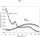
この光源を生体計測用に用いる場合には、被測定物質の特異的吸収波長を目安として波長を選ぶ必要がある。例えば還元型ヘモグロビン濃度を計測する場合に用いる光源の波長として、図3に示す還元型および酸素型ヘモグロビンの吸収係数を参考にすると、この物質の特異的吸収波長である760nmおよびこの近傍(例えば、800nm)の2波長を用いたり、この物質の吸収係数の差の大きな2種の波長とその中間の1波長との合計3波長を用いたりするとよい。図3よりその3波長のうち一つ目は、還元型ヘモグロビンの吸収係数の大きな730nm付近以下で信号強度を確保できるように生体の吸収の大きすぎない650nm以上の領域からひとつ(例えば690nm)を選ぶ。二つ目は酸化型ヘモグロビンの吸収係数の大きな830nm付近以上の領域からひとつ(例えば830nm)を選ぶ。三つ目は前記二つの波長の間で760nmを選ぶ。この波長は還元型ヘモグロビンの吸収係数が750nm〜760nmの間に極大値をもつことから、吸収される信号が大きくなり、計測精度向上に役立つ特異的吸収波長であるといえる。したがって、光源波長のひとつを750nm〜760nmに選ぶことには意味がある。 When this light source is used for biological measurement, it is necessary to select a wavelength based on the specific absorption wavelength of the substance to be measured. For example, referring to the absorption coefficient of reduced and oxygen hemoglobin shown in FIG. 3 as the wavelength of the light source used for measuring the reduced hemoglobin concentration, the specific absorption wavelength of this substance is 760 nm and its vicinity (for example, It is preferable to use two wavelengths (800 nm), or a total of three wavelengths including two wavelengths having a large difference in absorption coefficient of the substance and one intermediate wavelength. From FIG. 3, the first of the three wavelengths is one (for example, 690 nm) from the region of 650 nm or more where the absorption of the living body is not too high so that the signal intensity can be secured near 730 nm or less where the absorption coefficient of reduced hemoglobin is large. Choose. Secondly, one (for example, 830 nm) is selected from a region having a large absorption coefficient of oxidized hemoglobin and a region near 830 nm or more. The third is to select 760 nm between the two wavelengths. Since this wavelength has a maximum value between the absorption coefficient of reduced hemoglobin between 750 nm and 760 nm, it can be said that this wavelength is a specific absorption wavelength that increases the absorbed signal and is useful for improving measurement accuracy. Therefore, it is meaningful to select one of the light source wavelengths from 750 nm to 760 nm.
ところで、一つ目の波長を選ぶ際には、レーザ製品の放射安全基準(JIS C 6802)、世界基準(IEC 60825)を考慮して、700nm以上の波長を選ぶと同じクラスでも許容される強度を大きくでき、計測の信号を大きくすることができるため精度を上げることができる。このように、生体組織中での散乱が少ないことと安全上の基準を考慮しても測定精度を上げることができるので、波長を700nm以上にすることには意味がある。 By the way, when choosing the first wavelength, considering the radiation safety standard of laser products (JIS C 6802) and the world standard (IEC 60825), the intensity allowed even in the same class when selecting a wavelength of 700 nm or more Since the measurement signal can be increased and the measurement signal can be increased, the accuracy can be increased. As described above, the measurement accuracy can be improved even if the scattering in the living tissue is small and the safety standard is taken into consideration, so it is meaningful to set the wavelength to 700 nm or more.
図1の構成を持つ光源から発生した光は、そのまま光ファイバに導入して伝送させたり、空中伝播させたり、直接生体に照射してもよい。光ファイバに導入する場合は光ファイバ内で元の光出力が減衰されるので、ファイバ出力に対して安全上の配慮をした、光源光出力の設計が必要である。一方、空中伝播と生体照射の場合は、光源そのものの光出力に前記波長に応じた安全上の制限が加わる。前記安全基準により、観測者の目に対する安全を確保するために、焦点の合う最短距離である10cm離れたところでの瞳の大きさに相当する直径7mmの円内での光強度に制限があるため、レンズなどの光を広げる手段を用いて光を広げるとよい。 The light generated from the light source having the configuration shown in FIG. 1 may be introduced into an optical fiber as it is and transmitted, transmitted in the air, or directly irradiated on a living body. When the optical fiber is introduced into the optical fiber, the original optical output is attenuated in the optical fiber. Therefore, it is necessary to design a light source optical output in consideration of safety with respect to the fiber output. On the other hand, in the case of air propagation and living body irradiation, a safety restriction is added to the light output of the light source itself according to the wavelength. According to the safety standard, in order to ensure safety for the observer's eyes, there is a limit to the light intensity in a circle with a diameter of 7 mm corresponding to the size of the pupil at a distance of 10 cm, which is the shortest distance that is in focus. It is better to spread the light using a means of spreading the light such as a lens.
また、図3より還元型ヘモグロビンの805nm以下の領域の吸収係数は波長変動に対し敏感なので、波長変動は小さいほうがよい。通常半導体レーザのカタログでは波長の仕様は±10nmに設定されているが、光源を生体に近接して配置する場合は、温度変化が室温の25℃から、生体体温の約40℃に素子発熱分の10℃を加えた50℃程度までとなると考えると、温度変化に対する波長変動率は0.2nm/Kなので、波長変動を5nm程度にすることができる。これに作製ロットごとの活性層の組成ずれなど、作製上必要な余裕を持たせると、波長変動は倍の±5nm程度にすることができる。 Further, from FIG. 3, the absorption coefficient in the region of 805 nm or less of reduced hemoglobin is sensitive to wavelength fluctuations, so that the wavelength fluctuations should be small. Normally, in the catalog of semiconductor lasers, the wavelength specification is set to ± 10 nm. However, when the light source is placed close to the living body, the temperature changes from 25 ° C at room temperature to about 40 ° C at body temperature. Assuming that the temperature is up to about 50 ° C. by adding 10 ° C., the wavelength variation rate with respect to the temperature change is 0.2 nm / K, so the wavelength variation can be about 5 nm. If a margin necessary for production such as compositional deviation of the active layer for each production lot is provided, the wavelength fluctuation can be doubled to about ± 5 nm.
このような直接光源を被検体に照射する光計測装置では戻り光による光源の光出力変動は計測誤差につながるので、戻り光耐性を持つことが必要である。ひとつの解決方法は被検体からの反射戻り光が半導体レーザの共振器に入らないように、前端面の反射率を高く設定することが望ましい。端面発光型の半導体レーザの場合、よく知られている材料である、酸化珪素と窒化珪素とをそれぞれ四分の一波長の膜厚で積層すると約50%の高反射膜となる。さらに複数周期積み上げるとさらに高反射膜を作ることができ、よりよい戻り光耐性が得られる。また、面発光レーザでは半導体AlGaAsの積層膜で95%を超える反射率を用いることが多い。また、発光素子として発光ダイオードを用いることもでき、この場合は最初からコヒーレント光ではないので、戻り光には強い。 In such an optical measurement apparatus that directly irradiates a subject with a light source, fluctuations in the light output of the light source due to return light lead to measurement errors, and thus it is necessary to have resistance to return light. As one solution, it is desirable to set the reflectance of the front end face high so that reflected return light from the subject does not enter the resonator of the semiconductor laser. In the case of an edge-emitting semiconductor laser, when a well-known material, silicon oxide and silicon nitride, are laminated with a film thickness of a quarter wavelength, a high reflection film of about 50% is obtained. Further, when a plurality of cycles are stacked, a highly reflective film can be made and better return light resistance can be obtained. Further, in a surface emitting laser, a reflectance exceeding 95% is often used in a laminated film of semiconductor AlGaAs. In addition, a light emitting diode can be used as the light emitting element. In this case, since it is not coherent light from the beginning, it is strong against return light.
また、特に光源の反射率を低くして、前面からの光出力を多くしたい場合には、もうひとつの解決方法として、公知の技術であるセルフパルセーション動作により、縦モードを多モードにして結合しにくくすることができる。 Also, especially when you want to reduce the reflectance of the light source and increase the light output from the front surface, another solution is to combine the longitudinal mode into multiple modes by the self-pulsation operation that is a well-known technique. Can be difficult.
このような光源を用いて、生体に近接して生体情報を測定する場合には、生体に光源装置を密着させ、生体内で一部吸収されて戻った光を検出する検出器を光源位置に対して最適化された位置に配置したようなプローブを用いると位置決めがしやすい。光源装置は少なくとも2種類の異なる発光波長を持つ発光素子を含み、それぞれの発光素子を光らせるタイミングとしては周波数の異なる強度変調か時分割で動作させる。このような光源装置と検出器を複数個用意し、2次元的に配置したプローブを用いることで、広範囲の生体情報を一度に得ることもできる。 When measuring biological information in the vicinity of a living body using such a light source, a light source device is brought into close contact with the living body, and a detector that detects light that has been partially absorbed in the living body and returned to the light source position. On the other hand, using a probe arranged at an optimized position facilitates positioning. The light source device includes at least two kinds of light emitting elements having different light emission wavelengths, and the light emitting elements are operated by intensity modulation with different frequencies or time division as the timing for illuminating each light emitting element. By preparing a plurality of such light source devices and detectors and using a two-dimensionally arranged probe, a wide range of biological information can be obtained at once.
次に700nm〜760nmの波長で発振する半導体発光素子を実現する手段を詳しく述べる。
この波長範囲を満たすことのできる活性層として結晶成長方法が確立されていなかったために作製が困難であったGaAs基板上のInGaAsPを選ぶ。有機金属気層成長(MOVPE)装置を用いて、成長条件を実験的に最適化することでGaAs基板上にレーザの活性層相当の膜厚をもつInGaAsPを成長させることに成功した。成長条件はGaAs基板を用いた成長の常識的な範囲内のあるものであったが、装置ごとに最適化するべきものである。
Next, means for realizing a semiconductor light emitting device that oscillates at a wavelength of 700 nm to 760 nm will be described in detail.
As the active layer capable of satisfying this wavelength range, InGaAsP on the GaAs substrate, which has been difficult to produce because the crystal growth method has not been established, is selected. We succeeded in growing InGaAsP having a film thickness equivalent to the active layer of a laser on a GaAs substrate by experimentally optimizing the growth conditions using an organic metal vapor deposition (MOVPE) apparatus. The growth conditions are within a common sense of growth using a GaAs substrate, but should be optimized for each apparatus.
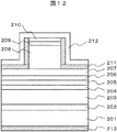
700nm〜760nmの波長で発振する半導体発光素子は図12を基本構成とする。n型GaAs基板201上に、n型GaAsバッファ層202、n型AlGaInPクラッド層203、n型AlGaInP光ガイド層204、歪量子井戸活性層205、p型AlGaInP光ガイド層206、第1p型AlGaInPクラッド層207、第2p型AlGaInPクラッド層208、p型GaInPキャップ層209、p型GaAsキャップ層210を、順次、MOVPE法で成長する。第2p型AlGaInPクラッド層208、p型GaInPキャップ層209、p型GaAsキャップ層210は、所定のエッチングによってストライプ形状に形成され、ストライプの側壁は絶縁膜211で保護される。また、p型GaAsキャップ層210上にはp電極212、n型GaAs基板201下にはn電極213が設けられる。
A semiconductor light emitting element that oscillates at a wavelength of 700 nm to 760 nm has a basic configuration shown in FIG. On an n-
上記歪量子井戸活性層205はIn1−xGaxAsyP1−y(0.10≦y≦0.45)量子井戸層(面内の格子定数aw)および(AlzGa1−z)wIn1−wP障壁層からなる。InGaAsP量子井戸層の歪量は、実験を行ない特性や信頼性を評価することで決定できる。理論計算および実験の結果、波長に関わらず、ε(%)=(aw−a)/a×100で定義される歪εは0.4%≦ε≦1.4%が望ましいことが明らかになった。特に、波長が700nm以上720nm以下の場合は、0.4%≦ε≦1.2%が望ましく、さらに0.4%≦ε≦0.9%が最適範囲である。また、波長が725nm以上760nm以下の場合は、0.6%≦ε≦1.4%の歪の範囲が望ましいことが明らかになった。
なお、上記GaAs基板201は面方位が(100)面から<011>方向へ傾いたオフ基板でも良く、また、上記歪量子井戸活性層205は、障壁層に引張り歪を加えた歪補償構造でも良い。
The strained quantum well
The
ここで、本発明と従来技術との差異を述べる。
特許文献1は生体の情報を得るために、光計測に先立ってCT計測が必要であるが、本発明では、光計測のみで生体情報を得る。特許文献2は光計測により生体情報を時系列表示できるが、その光源については波長以外の詳細な記述がない。本発明では特許文献2の信号処理理論をそのまま用いて、光計測装置に用いる光源の構成と光出力安定化の制御を提案した。
Here, the difference between the present invention and the prior art will be described.
In
特許文献3、4、7は複数の半導体発光素子を搭載した半導体光源で、主な用途が光記録および光書込であるため、それぞれの発光点を同時に光らせて使用する用法はないが、本発明は複数の異なる波長を持つ半導体発光素子を同時に発光させて用いる。特許文献7とはひとつの光出力モニタ素子を用いている点は共通であるが、ある特定の時間に光っている1つの素子のみに制御信号を返して光出力を安定化させる構成であるのに対し、本発明は同時に複数の半導体発光素子を光らせ、それぞれを異なる周波数または時分割で動作させることでひとつの光出力モニタ素子に入った信号を分離してそれぞれの半導体発光素子の光出力安定化ができるようになっており、光出力安定化に関する構成が異なる。
この光出力安定化方法の構成により、特許文献5とも区別できる。なぜなら、特許文献5では複数の波長の異なる半導体発光素子を搭載した半導体光源で、主な用途はディスプレイのため、複数の発光素子を同時に発光させることがあるが、それぞれの発光素子の光出力を測定するために同数の光出力モニタ素子が用意されている。本発明ではそのことを安定化させるための課題として挙げて、ひとつの光出力モニタ素子に入った信号を分離する構成としている。 The configuration of this light output stabilization method can be distinguished from Patent Document 5. This is because Patent Document 5 is a semiconductor light source equipped with a plurality of semiconductor light-emitting elements having different wavelengths, and the main application is for a display, so that a plurality of light-emitting elements may emit light simultaneously. The same number of light output monitoring elements are prepared for measurement. In the present invention, as a problem for stabilizing this, a configuration is adopted in which a signal entering one light output monitor element is separated.
特許文献6は複数の発光素子の前方で行路の途中に光出力モニタ素子を置いているが、本発明は、光源を生体に近接させる用法を含むため行路の途中に光出力モニタ素子を置くことができず、発光素子の発光点より後方に光出力モニタ素子を置いた。 In Patent Document 6, a light output monitor element is placed in the middle of a path in front of a plurality of light emitting elements. However, the present invention includes a method of bringing a light source close to a living body, and therefore, the light output monitor element is placed in the middle of the path. The light output monitoring element was placed behind the light emitting point of the light emitting element.
特許文献8の半導体発光素子は活性層にInGaAsPを用いているが、発光波長が635nmで、従来技術でも安定に結晶成長できる範囲の組成を用いており、同じ構成では本発明の700nm以上の波長帯での組成を達成することができない。一方、非特許文献2は本発明と発光波長帯は同じであるが、本発明では、より信頼性の高い、発光波長700nm〜760nmの発光素子を与える結晶の供給を実現するために、歪に着目して組成の限定を加えたことが従来と異なる。
The semiconductor light emitting device of
これら、従来の技術をすべて組み合わせても、生体に近接して情報を計測する場合には対応できず、本発明では、生体に近接して光源と生体からの信号を検出する検出器とを配置し、光源を光らせるタイミングを選ぶ方式と光出力安定化および発光波長安定化について言及している点が従来と異なる。 Even if all of these conventional techniques are combined, it is not possible to measure when measuring information close to a living body, and in the present invention, a light source and a detector that detects a signal from the living body are arranged close to the living body. However, it differs from the conventional system in that it refers to a method for selecting the timing for illuminating the light source and stabilization of light output and light emission wavelength.
また、発光波長700nm〜760nmの発光素子を高信頼の半導体発光素子で供給することができなかったため、従来はこれとは異なる波長範囲の半導体光源を生体光計測に用いていた。本発明による高信頼性の得られる構成によって初めて発光波長700nm〜760nmの発光素子を生体光計測の光源として用いることができるようになった。 In addition, since a light-emitting element having an emission wavelength of 700 nm to 760 nm could not be supplied by a highly reliable semiconductor light-emitting element, a semiconductor light source having a wavelength range different from this was conventionally used for biological light measurement. For the first time, a light-emitting element having an emission wavelength of 700 nm to 760 nm can be used as a light source for living body light measurement by a configuration with high reliability according to the present invention.
生体光計測装置として、半導体発光素子の入ったカンパッケージを複数個並べるのに比べ、複数波長の半導体発光素子の入ったひとつのカンパッケージを使用するので小型・軽量化できる。また、前記半導体光素子の光出力検出用にひとつの光出力モニタ素子を前記複数の発光素子を近接して搭載した後方に配置して、前記複数の発光素子からの信号を分離する回路を持つことにより、隣接素子の影響を分離できる。そして、生体計測用光源として、これまで実現困難であった700nm〜760nmの波長の半導体レーザを供給することができる。 Compared to arranging a plurality of can packages containing semiconductor light emitting elements as a biological light measuring device, one can package containing semiconductor light emitting elements having a plurality of wavelengths is used, so that the size and weight can be reduced. Also, there is a circuit for separating a signal from the plurality of light emitting elements by arranging one light output monitoring element for detecting the light output of the semiconductor optical element behind the plurality of light emitting elements. Thus, the influence of adjacent elements can be separated. A semiconductor laser having a wavelength of 700 nm to 760 nm, which has been difficult to realize until now, can be supplied as a biological measurement light source.
以下、本発明の実施例について、図面を参照して詳述する。 Hereinafter, embodiments of the present invention will be described in detail with reference to the drawings.
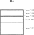
本発明の第1の実施例を、図1、および図2に示す装置に従い説明する。半導体レーザ1〜3はそれぞれ有機金属気相成長(MOVPE)装置を用いて、図4に断面構造を示すようにn型GaAs基板101上にn型クラッド層102、活性層103、p型クラッド層104、p型コンタクト層105の順に結晶成長する。3個の半導体レーザのうち発振波長760nm以下を狙う1、2は、p型、n型クラッド層102、104に厚さ1.5μmのAlGaInP層を用いて、活性層103には厚さ10nmのGaIn(As)Pの井戸層と厚さ15nmのAlGaInPの障壁層からなる多重量子井戸構造とそれを挟んだ厚さ25nmのAlGaInP層からなる光ガイド層を持ち、p型コンタクト層105にはGaAs層を用いる。残りの1個の発振波長800nm台を狙う半導体レーザ3は、p型、n型クラッド層102、104に厚さ1.5μmのAlGaAs層を用いて、活性層103には厚さ10nmのGaAsの井戸層と厚さ15nmのAlGaAsの障壁層からなる多重量子井戸構造とそれを挟んだ厚さ25nmのAlGaAs層からなる光ガイド層を持ち、p型コンタクト層105にはGaAs層を用いる。
A first embodiment of the present invention will be described with reference to the apparatus shown in FIGS. Each of the
フォトリソグラフィー工程により、ストライプ状のパターニングをした後、ドライエッチング装置によりストライプを残してエッチングし、メサ形状を形成する。半導体レーザ3のみ、ストライプのパターニングをしたときに用いたマスクを利用してMOVPE装置による選択成長でストライプ以外の部分にn型ドープAlGaAsとn型ドープGaAsからなるブロック層を成長させ、マスクを除去した後、p型ドープGaAsコンタクト層を成長させてメサを埋め込む。
Stripe patterning is performed by a photolithography process, and then etching is performed with a dry etching apparatus leaving a stripe, thereby forming a mesa shape. Only for the
ストライプ以外の場所に厚さ350nmの酸化珪素膜によるパッシベーションを施し、p側電極となるチタン、白金、金を順に電子ビーム蒸着する。GaAs基板の裏面を研磨して厚さ100μmとしてから、裏面にn側電極となる金―ゲルマニウム、ニッケル、チタン、白金、金を順に電子ビーム蒸着したあと、合金化する。各ウェハは半導体レーザの共振器長が800μmとなるように劈開する。劈開端面にはスパッタリング装置で、前面にアルミナを付着させ反射率を13%程度とし、後面にはアルミナと酸化チタンの積層膜を付着させ反射率を90%以上とした。 Passivation with a silicon oxide film having a thickness of 350 nm is performed at a place other than the stripe, and titanium, platinum, and gold to be a p-side electrode are sequentially deposited by electron beam. After the back surface of the GaAs substrate is polished to a thickness of 100 μm, gold-germanium, nickel, titanium, platinum, and gold, which are n-side electrodes, are sequentially deposited on the back surface by electron beam evaporation and alloyed. Each wafer is cleaved so that the cavity length of the semiconductor laser becomes 800 μm. A sputtering apparatus was used to deposit alumina on the front face of the cleavage end face to give a reflectance of about 13%, and a laminated film of alumina and titanium oxide was made to adhere to the rear face to make the reflectance 90% or more.
こうして作製した半導体レーザ1〜3をジャンクションダウンでサブマウント4に実装する。ヒートシンク10には半導体レーザの光出力安定化のための光出力モニタ素子としてモニタ用フォトダイオード(以下、モニタPD)9を先に半田で固定してから、半導体レーザ1〜3を実装したサブマウント4を半田で固定する。半導体レーザ1〜3からの配線を電極パッド5〜8を介してヒートシンクの入出力側ピンに接続する。図1ではカソードコモンの接続を例に示しているが、アノードコモンとしてもよく、まったく同様に制御可能である。このあとキャップ(図示せず)をつけて封じることでカンパッケージが完成する。モニタPD9からの出力はモニタ信号分離回路11へ導かれ、ここで分離された信号は半導体レーザ1〜3の駆動電源12〜14にフィードバックされ光出力変動をなくすように補正をかけられる。
ここでは、生体計測の分光分析の精度を上げるために、半導体レーザ1〜3は、非常に近いが異なる周波数で変調されており、このときモニタ信号分離回路11としてはロックインアンプを用いるとよい。
The
Here, in order to increase the accuracy of the spectroscopic analysis of the biological measurement, the
本実施例で作製した半導体レーザ1〜3の発振波長はそれぞれ、690nm、760nm、830nmで、25℃から50℃において光出力50mWで動作し、その温度範囲の発振波長の変動は±5nm以内であった。また、50℃、50mWでの一定光出力の寿命試験では2000時間以上の動作を確認した。さらに、各半導体レーザを異なる周波数で変調して、後方で受光した光出力モニタ信号はロックインアンプを用いて分離することができ、半導体レーザ駆動電源12〜14にフィードバックすることにより、光出力の変動量は0.1%以下に抑えることができた。
The oscillation wavelengths of the
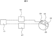
本発明の第2の実施例を、図5に示す生体光計測装置に従い説明する。複数波長の半導体レーザを搭載した光源15は、第1の実施例と同様の作製方法で得られる。制御・表示用パソコン17により制御された、送信機18内のパルス発生器19によるパルス信号をCDMAエンコード回路20により変調信号として、光源ドライバ16に供給して、光源15を駆動する。この光源15は発振波長695nm、780nm、850nmで発振し、25℃から60℃において光出力50mWでは光出力変動量0.1%以下で動作する。この光源15から発光される3波長の光は発光点間隔が220μmで、この光を直径1mmのコア部分を持つバンドルファイバ21に導入する。そのファイバ出力光を周波数変調して生体22に照射し、生体物質での光吸収後に戻ってきた光を受光素子モジュール23で捉える。この光源15と受光素子モジュール23は信号処理に最適な間隔でプローブ24に着脱可能な状態で固定されており、生体22の表面での位置決めが容易であると同時に、故障時のモジュール交換が可能となっている。アナログ増幅器25とCDMAデコード回路26をあわせた受信機27を用いて信号処理を行い、生体からの信号として制御・表示用パソコン17で解析・表示する。光源15の光出力変動が小さいので、信号の信頼度を高くすることができた。
A second embodiment of the present invention will be described with reference to the biological light measurement apparatus shown in FIG. The
本発明の第3の実施例は、図5に示す装置と同じ構成である。複数波長の半導体レーザを搭載した光源15は、第1の実施例と同様の作製方法で得られ、発振波長680nm、755nm、830nmで発振し、25℃から60℃において光出力50mWでは光出力変動量0.1%以下で動作する。この波長の選び方は、図3により還元型ヘモグロビンの吸収係数が非常に大きい680nmと酸化型ヘモグロビンの吸収係数が比較的大きい830nmとその中間の波長755nmである。この光源15から発光される3波長の光を直径1mmのコア部分を持つバンドルファイバ21に導入する。そのファイバ出力光を周波数変調して生体22に照射し、生体物質での光吸収後に戻ってきた光を受光素子モジュール23で捉え、第2の実施例と同様に受信機27により信号処理を行い、生体からの信号として解析する。光源15の光出力変動が小さく、計測対象の還元型ヘモグロビンと酸化型ヘモグロビンの吸収係数の差の大きな2波長とその中間の波長を選んでいるので精度よく測定することができた。
The third embodiment of the present invention has the same configuration as the apparatus shown in FIG. A
本発明の第4の実施例は、図1に示した光源装置の半導体レーザの波長を限定したものである。半導体レーザ1、2、3の発振波長はそれぞれ705±5nm、755±5nm、830±5nmとなるように活性層組成を決める。半導体レーザ1、2は活性層にInGaAsPの井戸層を持つ量子井戸構造を用いて製造し、半導体レーザ3は活性層にGaAsの井戸層を持つ量子井戸構造を用いて製造すればよい。
In the fourth embodiment of the present invention, the wavelength of the semiconductor laser of the light source device shown in FIG. 1 is limited. The active layer composition is determined so that the oscillation wavelengths of the
特に、生体組織中での散乱が少なく水による吸収が少ない700nm〜1300nmの波長を選択しているため精度よく生体からの信号を取り出すことができた。この中の半導体レーザ1は最も短い波長705±5nmを持つが、生体組織中での散乱が少ないことと安全上の基準を考慮した700nm以上の波長で最大限に還元型ヘモグロビンの吸収係数の大きい波長である。また、半導体レーザ2は、還元型ヘモグロビンの吸収係数が極大値を持つ特異的吸収波長である750〜760nmの波長で発振するため、吸収される信号が大きくなる。これらのことから半導体レーザの発振波長として705±5nm、755±5nmを選ぶことは測定精度向上に役立っている。
In particular, since a wavelength of 700 nm to 1300 nm with little scattering in living tissue and little absorption by water is selected, signals from the living body can be extracted with high accuracy. Among them, the
本発明の第5の実施例を、図6、および7に示す装置に従い説明する。図6は本発明の光源を発光面から見た図であり、図7はそれを横から見た断面図である。半導体レーザ120、121、122は垂直共振器面発光型レーザで、波長は780nm、805nm、830nmである。これらの半導体レーザはサブマウント123の上に実装され、モニタPD124とともにヒートシンク125に固定されている。その後、上記波長における反射率が10%程度で光伝播方向に対して垂直から若干傾いた窓の付いたキャップ126で封じる。この光源28はこれらの3つの波長のおのおので光出力2mWが得られた。
A fifth embodiment of the present invention will be described with reference to the apparatus shown in FIGS. 6 is a view of the light source of the present invention as seen from the light emitting surface, and FIG. 7 is a cross-sectional view of the light source as seen from the side. The
光出力を安定化する構成は図8を用いて説明する。モニタPD124からの出力はモニタ信号分離回路11へ導かれ、ここで分離された信号は半導体レーザ120〜122の光源ドライバ16にフィードバックされ光出力変動をなくすように補正をかけられる。ここでは、生体計測の分光分析の精度を上げるために、半導体レーザ120〜122は、時分割で駆動されており、このときモニタ信号はモニタ信号分離回路11によって半導体レーザ120〜122に同期した信号のみが検出される。この全体で光源モジュール29を形成する。
A configuration for stabilizing the light output will be described with reference to FIG. The output from the
本実施例の光源は生体から数mmの距離に近接して使用され、使用温度がほぼ40℃に保たれていたため、波長変動が小さく、素子ごとに±5nm以内の変動であった。また、面発光型レーザでは光の放出面の反射率が約95%のため、戻り光耐性があり、光出力変動が0.05%以内であった。このことから安定して雑音の少ない生体からの信号を得ることができた。 Since the light source of this example was used close to a distance of several mm from the living body and the use temperature was kept at approximately 40 ° C., the wavelength variation was small, and the variation was within ± 5 nm for each element. In addition, since the reflectance of the light emitting surface is about 95% in the surface emitting laser, the surface emitting laser is resistant to return light, and the light output fluctuation is within 0.05%. From this, it was possible to obtain a stable signal from a living body with little noise.
なお、半導体レーザ120、121、122は発光ダイオードに置き換えてもよい。それは発光ダイオードがコヒーレント光でないために、垂直共振器面発光型レーザと同等の良好な戻り光耐性を持つためである。
The
本発明の第6の実施例を、図9に示す装置に従い説明する。複数波長の半導体レーザを搭載した光源モジュール29は第5の実施例と同様の作製方法で得られ、ここでは発振波長780nm、830nmの2種類の波長で発振し、使用温度25℃から40℃の範囲では、光出力2mWで、波長変動は±5nm以内、光出力変動は0.05%以内であった。この光源モジュール29は送信機18により動作のタイミングを決める信号を受け、生体22に光を照射する。生体物質での光吸収後に戻ってきた光を受光素子モジュール23で捉える。その信号を受信機27で信号処理し、生体からの信号として制御・表示用パソコン17で解析・表示する。
A sixth embodiment of the present invention will be described with reference to the apparatus shown in FIG. A
この光源モジュール29と受光素子モジュール23は信号処理に最適な間隔でプローブ24に着脱可能な状態で固定されており、生体22の表面での位置決めが容易であると同時に、故障時のモジュール交換が可能となっている。プローブ24の断面の一部は図10に示すようになっている。光源モジュール29は光源28とその光出力安定化回路30とともにケース31に入っており、給電コネクタ32で外から電源供給を受ける。受光素子モジュール23はアバランシェフォトダイオード33と増幅器や高圧電源部を含む制御回路34とがケース31に入っており、給電コネクタ32で外から電源供給を受ける。ケース31はプローブ24から着脱可能となっている。図には光源モジュール29と受光素子モジュール23が2個ずつ固定されているが、さらに多くのモジュールをアレイ状に配置して、生体からの広い面積の信号を得ることもできる。
The
光源モジュール29が生体に光を導入するための光ファイバを不要とし小型軽量化できたために、生体光計測装置の小型化が実現し、従来どおりの測定精度も実現することができた。
Since the
本発明の第7の実施例を、図11に示す装置に従い説明する。半導体レーザ130は公知の2波長集積半導体レーザの技術で作製された端面発光型レーザであり、発振波長は690nm、760nmである。光の放出端面の反射率は酸化珪素と窒化珪素の四分の一波長積層膜を2周期形成することにより68%とした。光出力はそれぞれの波長で4mWが得られた。観測者の目に直接入ることを想定したときの安全性の問題を回避するために、光源のパッケージには光を広げる手段、たとえばレンズ131を持つ。
A seventh embodiment of the present invention will be described with reference to the apparatus shown in FIG. The
光出力を安定化する構成は図8の構成と同じである。半導体レーザ130は、時分割で駆動されており、このときモニタ信号は図8に示すモニタ信号分離回路11と同様の回路によって半導体レーザ130の各波長の光に同期した信号のみが検出される。ここで、計測精度を上げるためには複数の波長で同時に光っているほうが、同じ時刻での複数の信号を得られるために望ましく、半導体レーザ130の各波長の光を異なる周波数で強度変調し、モニタ信号を分離する回路11としてロックインアンプを用いて各波長の光強度を安定化する方法を使ってもよい。さらに精度を上げるために、時分割および、異なる周波数での強度変調との両方の駆動タイミングを掛け合わせたもので、複数の波長の光を駆動してもよい。いずれにしても発光素子の駆動タイミングにあわせて、モニタPD9に入った信号を分離するように図8に示すモニタ光出力分離回路11と同様の回路を作ればよい。
The configuration for stabilizing the light output is the same as the configuration in FIG. The
本実施例の光源は生体から数mmの距離に近接して使用され、使用温度がほぼ40℃に保たれていたため、波長変動が小さく、素子ごとに±5nm以内の変動であった。光の放出面の反射率が68%のため、戻り光耐性があり、光出力変動が0.08%以内であった。このことから安定して雑音の少ない生体からの信号を得ることができた。 Since the light source of this example was used close to a distance of several mm from the living body and the use temperature was kept at approximately 40 ° C., the wavelength variation was small, and the variation was within ± 5 nm for each element. Since the reflectivity of the light emission surface was 68%, the light output resistance was high, and the light output fluctuation was within 0.08%. From this, it was possible to obtain a stable signal from a living body with little noise.
本発明の第8の実施例を、図11を用いて説明する。ここでは半導体レーザ130は光を放出する端面付近に過飽和領域を設けることによりパルセーション動作を発生させることにより戻り光耐性を高くしている。光出力を安定化させるのは例えば図2の構成と同様に、各半導体レーザを異なる周波数で駆動して、モニタPDの信号をロックインアンプで分離するとよい。
An eighth embodiment of the present invention will be described with reference to FIG. Here, the
本実施例の光源は生体から数mmの距離に近接して使用され、使用温度がほぼ40℃に保たれていたため、波長変動が小さく、素子ごとに±5nm以内の変動であった。パルセーション動作ため戻り光が結合しにくく、光出力変動が0.08%以内であった。このことから安定して雑音の少ない生体からの信号を得ることができた。 Since the light source of this example was used close to a distance of several mm from the living body and the use temperature was kept at approximately 40 ° C., the wavelength variation was small, and the variation was within ± 5 nm for each element. Because of the pulsation operation, it was difficult for the return light to be coupled, and the light output fluctuation was within 0.08%. From this, it was possible to obtain a stable signal from a living body with little noise.
第9の実施例について、半導体レーザの断面構造図(図12)を使って説明する。所定のn型GaAs基板201上に、n型GaAsバッファ層202、n型AlGaInPクラッド層203、n型AlGaInP光ガイド層204、歪量子井戸活性層205、p型AlGaInP光ガイド層206、第1p型AlGaInPクラッド層207、第2p型AlGaInPクラッド層208、p型GaInPキャップ層209、p型GaAsキャップ層210が、順次、有機金属気相成長法(MOVPE法)で積層される。第2p型AlGaInPクラッド層208、p型GaInPキャップ層209、p型GaAsキャップ層210は、所定のエッチングによってストライプ形状に形成され、ストライプの側壁は絶縁膜211で保護される。また、p型GaAsキャップ層210上にはp電極212、n型GaAs基板201にはn電極213が設けられる。
The ninth embodiment will be described with reference to a sectional view of a semiconductor laser (FIG. 12). On a predetermined n-
第9の実施例では、上記歪量子井戸活性層205はIn0.5Ga0.5As0.16P0.84量子井戸(圧縮歪0.7%)および(Al0.5Ga0.5)0.5In0.5P障壁層からなる。この場合、量子井戸幅を7〜12nmの間で調整することによって波長705nmで発振する半導体レーザ装置が得られる。
In the ninth embodiment, the strained quantum well
これを第1の実施例の半導体レーザ1に適用することで生体光計測に適した光源を供給することができる。
By applying this to the
第10の実施例について、半導体レーザの断面構造図(図12)を使って説明する。本実施例では、上記歪量子井戸活性層205はIn0.5Ga0.5As0.32P0.68量子井戸(圧縮歪1.2%)および(Al0.5Ga0.5)0.5In0.5P障壁層からなる。この場合、量子井戸幅を7〜12nmの間で調整することによって波長755nmで発振する半導体レーザ装置が得られる。
これを第1の実施例の半導体レーザ2に適用することで生体光計測に適した光源を供給することができる。
A tenth embodiment will be described with reference to a sectional view of a semiconductor laser (FIG. 12). In this embodiment, the strained quantum well
By applying this to the
なお、上記GaAs基板201は面方位が(100)面から<011>方向へ傾いたオフ基板でも良く、また、上記歪量子井戸活性層205は、障壁層に引張り歪を加えた歪補償構造でも良い。また、上記InGaAsP量子井戸層の歪量は、実験を行ない特性や信頼性を評価することで決定できる。理論計算および実験の結果、波長に関わらず、0.4%≦ε≦1.4%が望ましいことが明らかになった。特に、波長が700nm以上720nm以下の場合は、0.4%≦ε≦1.2%が望ましく、さらに0.4%≦ε≦0.9%が最適範囲である。また、波長が725nm以上760nm以下の場合は、0.6%≦ε≦1.4%の歪の範囲が望ましいことが明らかになった。
The
なお、本実施例およびその変形で実現できるのは下記の半導体レーザ装置である。
1.格子定数aを有するGaAs基板上に設けられ、面内の格子定数awを有するIn1−xGaxAsyP1−y量子井戸層および障壁層からなる発光層を有し、前記発光層は、前記量子井戸層がε(%)=(aw−a)/a×100で定義される歪εが0.4%≦ε≦1.4%で、その組成が0.10≦y≦0.45であり、発光する波長が700nm以上760nm以下であることを特徴とする半導体レーザ装置。
2.格子定数aを有するGaAs基板上に設けられ、面内の格子定数awを有するIn1−xGaxAsyP1−y量子井戸層および障壁層からなる発光層を有し、前記発光層は、前記量子井戸層がε(%)=(aw−a)/a×100で定義される歪εが0.4%≦ε≦1.2%で、その組成が0.10≦y≦0.25であり、発光する波長が700nm以上730nm以下であることを特徴とする半導体レーザ装置。
3.格子定数aを有するGaAs基板上に設けられ、面内の格子定数awを有するIn1−xGaxAsyP1−y量子井戸層および障壁層からなる発光層を有し、前記発光層は、前記量子井戸層がε(%)=(aw−a)/a×100で定義される歪εが0.4%≦ε≦0.9%で、その組成が0.10≦y≦0.2であり、発光する波長が700nm以上720nm以下であることを特徴とする半導体レーザ装置。
4.格子定数aを有するGaAs基板上に設けられ、面内の格子定数awを有するIn1−xGaxAsyP1−y量子井戸層および障壁層からなる発光層を有し、前記発光層は、前記量子井戸層がε(%)=(aw−a)/a×100で定義される歪εが0.6%≦ε≦1.4%で、その組成が0.20≦y≦0.35であり、発光する波長が700nm以上760nm以下であることを特徴とする半導体レーザ装置。
5.格子定数aを有するGaAs基板上に設けられ、面内の格子定数awを有するIn1−xGaxAsyP1−y量子井戸層および障壁層からなる発光層を有し、前記発光層は、前記量子井戸層がε(%)=(aw−a)/a×100で定義される歪εが0.1%≦ε≦0.45%で、その組成が0.4≦y≦1.4であり、発光する波長が700nm以上760nm以下であることを特徴とする半導体レーザ装置。
6.格子定数aを有するGaAs基板上に設けられ、面内の格子定数awを有するIn1−xGaxAsyP1−y量子井戸層および障壁層からなる発光層を有し、前記発光層は、前記量子井戸層がε(%)=(aw−a)/a×100で定義される歪εが0.4%≦ε≦1.2%で、その組成が0.10≦y≦0.25であり、発光する波長が700nm以上730nm以下であることを特徴とする半導体レーザ装置。
7.所定のGaAs基板(格子定数a)上に設けられた、In1−xGaxAsyP1−y量子井戸層(面内の格子定数aw)および障壁層からなる発光層において、ε(%)=(aw−a)/a×100で定義される歪εが0.4%≦ε≦0.9%、量子井戸層の組成が0.10≦y≦0.20、波長が700nm以上720nm以下であることを特徴とする半導体発光装置を搭載したことを特徴とする半導体レーザ装置。
8.所定のGaAs基板(格子定数a)上に設けられた、In1−xGaxAsyP1−y量子井戸層(面内の格子定数aw)および障壁層からなる発光層において、ε(%)=(aw−a)/a×100で定義される歪εが0.6%≦ε≦1.4%、量子井戸層の組成が0.20≦y≦0.35、波長が725nm以上760nm以下であることを特徴とする半導体発光装置を搭載したことを特徴とする半導体レーザ装置。
The following semiconductor laser device can be realized by this embodiment and its modifications.
1. A light-emitting layer provided on a GaAs substrate having a lattice constant a and having an in-plane lattice constant aw and comprising an In 1-x Ga x As y P 1-y quantum well layer and a barrier layer; In the quantum well layer, the strain ε defined by ε (%) = ( aw− a) / a × 100 is 0.4% ≦ ε ≦ 1.4%, and the composition is 0.10 ≦ y. ≦ 0.45, and the wavelength of light emission is 700 nm or more and 760 nm or less.
2. A light-emitting layer provided on a GaAs substrate having a lattice constant a and having an in-plane lattice constant aw and comprising an In 1-x Ga x As y P 1-y quantum well layer and a barrier layer; In the quantum well layer, the strain ε defined by ε (%) = ( aw− a) / a × 100 is 0.4% ≦ ε ≦ 1.2%, and the composition is 0.10 ≦ y. ≦ 0.25, and the wavelength of light emission is 700 nm or more and 730 nm or less.
3. A light-emitting layer provided on a GaAs substrate having a lattice constant a and having an in-plane lattice constant aw and comprising an In 1-x Ga x As y P 1-y quantum well layer and a barrier layer; In the quantum well layer, the strain ε defined by ε (%) = ( aw− a) / a × 100 is 0.4% ≦ ε ≦ 0.9%, and the composition is 0.10 ≦ y. ≦ 0.2, and a light emitting wavelength is 700 nm or more and 720 nm or less.
4). A light-emitting layer provided on a GaAs substrate having a lattice constant a and having an in-plane lattice constant aw and comprising an In 1-x Ga x As y P 1-y quantum well layer and a barrier layer; In the quantum well layer, the strain ε defined by ε (%) = ( aw− a) / a × 100 is 0.6% ≦ ε ≦ 1.4%, and the composition is 0.20 ≦ y. ≦ 0.35, and the wavelength of light emission is 700 nm or more and 760 nm or less.
5. A light-emitting layer provided on a GaAs substrate having a lattice constant a and having an in-plane lattice constant aw and comprising an In 1-x Ga x As y P 1-y quantum well layer and a barrier layer; In the quantum well layer, the strain ε defined by ε (%) = ( aw− a) / a × 100 is 0.1% ≦ ε ≦ 0.45%, and the composition is 0.4 ≦ y. ≦ 1.4, and the wavelength of the emitted light is 700 nm or more and 760 nm or less.
6). A light-emitting layer provided on a GaAs substrate having a lattice constant a and having an in-plane lattice constant aw and comprising an In 1-x Ga x As y P 1-y quantum well layer and a barrier layer; In the quantum well layer, the strain ε defined by ε (%) = ( aw− a) / a × 100 is 0.4% ≦ ε ≦ 1.2%, and the composition is 0.10 ≦ y. ≦ 0.25, and the wavelength of light emission is 700 nm or more and 730 nm or less.
7). In a light emitting layer comprising an In 1-x Ga x As y P 1-y quantum well layer (in-plane lattice constant a w ) and a barrier layer provided on a predetermined GaAs substrate (lattice constant a), ε ( %) = (A w −a) / a × 100 The strain ε is 0.4% ≦ ε ≦ 0.9%, the composition of the quantum well layer is 0.10 ≦ y ≦ 0.20, and the wavelength is A semiconductor laser device comprising a semiconductor light emitting device having a thickness of 700 nm to 720 nm.
8). In a light emitting layer comprising an In 1-x Ga x As y P 1-y quantum well layer (in-plane lattice constant a w ) and a barrier layer provided on a predetermined GaAs substrate (lattice constant a), ε ( %) = ( Aw− a) / a × 100, the strain ε is 0.6% ≦ ε ≦ 1.4%, the composition of the quantum well layer is 0.20 ≦ y ≦ 0.35, and the wavelength is A semiconductor laser device comprising a semiconductor light emitting device having a wavelength of 725 nm to 760 nm.
本発明は、複数の波長の光を用いた高精度生体計測およびその光源として用いることができる。 The present invention can be used as a highly accurate living body measurement using a plurality of wavelengths of light and a light source thereof.
1,2,3:半導体レーザ素子、4:サブマウント、5,6,7,8:電極配線用パッド、9:半導体レーザ光出力光出力モニタ素子、10:ヒートシンク、11:モニタ信号分離回路、12,13,14:発光素子駆動電源、15:光源、16:光源ドライバ、17:制御・表示用パソコン、18:送信機、19:パルス発生器、20:CDMAエンコード回路、21バンドルファイバ、22生体、23:受光素子モジュール、24:プローブ、25:アナログ増幅器、26:CDMAデコード回路、27:受信機、28:光源、29:光源モジュール、30:光出力安定化回路、31:ケース、32給電コネクタ、33:アバランシェフォトダイオード、34:制御回路、101:n型GaAs基板、102:n型クラッド層、103:活性層、104:p型クラッド層、105:p型コンタクト層、120,121:垂直共振器面発光型レーザ、122:垂直共振器面発光型レーザ、123:サブマウント、124:半導体レーザ光出力光出力モニタ素子、125:ヒートシンク、126:キャップ、130:半導体レーザ素子、131:レンズ、201:n型GaAs基板、202:n型GaAsバッファ層、203:n型AlGaInPクラッド層、204:n型AlGaInP光ガイド層、205:歪量子井戸活性層、206:p型AlGaInP光ガイド層、207:第1p型AlGaInPクラッド層、208:第2p型AlGaInPクラッド層、209:p型GaInPキャップ層、210:p型GaAsキャップ層、211:絶縁膜、212:p電極、213:n電極。 1, 2, 3: semiconductor laser element, 4: submount, 5, 6, 7, 8: electrode wiring pad, 9: semiconductor laser light output light output monitor element, 10: heat sink, 11: monitor signal separation circuit, 12, 13, 14: Light-emitting element drive power supply, 15: Light source, 16: Light source driver, 17: Personal computer for control and display, 18: Transmitter, 19: Pulse generator, 20: CDMA encoding circuit, 21 bundle fiber, 22 Living body, 23: light receiving element module, 24: probe, 25: analog amplifier, 26: CDMA decoding circuit, 27: receiver, 28: light source, 29: light source module, 30: light output stabilization circuit, 31: case, 32 Feed connector 33: Avalanche photodiode 34: Control circuit 101: n-type GaAs substrate 102: n-type cladding layer 103: active layer 1 04: p-type cladding layer, 105: p-type contact layer, 120, 121: vertical cavity surface emitting laser, 122: vertical cavity surface emitting laser, 123: submount, 124: semiconductor laser light output light output monitor Element: 125: Heat sink 126: Cap 130: Semiconductor laser element 131: Lens 201: n-type GaAs substrate 202: n-type GaAs buffer layer 203: n-type AlGaInP cladding layer 204: n-type AlGaInP light guide Layer, 205: strained quantum well active layer, 206: p-type AlGaInP light guide layer, 207: first p-type AlGaInP clad layer, 208: second p-type AlGaInP clad layer, 209: p-type GaInP cap layer, 210: p-type GaAs Cap layer, 211: insulating film, 212: p electrode, 213: n electrode.
Claims (10)
前記生体の内部を前記複数の光信号が通過して該生体の表面から放出される複数の光信号を検出する受光素子と、を備え、
前記光源装置は、サブマウント上に搭載され可視から赤外の波長範囲で互いに異なる波長を有する複数の半導体発光素子と、
前記複数の半導体発光素子に接続され光信号出力を制御して、異なる波長の光信号を放出させる駆動用回路と、
前記複数の半導体発光素子から放射される各々の光信号出力を検知する一つの光出力モニタ素子とが一つに収納されたパッケージを具備してなり、
前記一つの光出力モニタ素子で検出された複数の光信号を、該それぞれの波長を発する前記半導体発光素子に接続された前記駆動用回路の各々に帰還させることにより、前記複数の半導体発光素子の光信号出力の制御を行い、
前記パッケージはプローブに着脱可能な状態で固定され、
前記半導体発光素子の少なくとも一つが、格子定数aを有するGaAs基板上に設けられ、面内の格子定数a w を有するIn 1−x Ga x As y P 1−y 量子井戸層および障壁層からなる発光層を有し、
前記発光層は、前記量子井戸層がε(%)=(a w −a)/a×100で定義される歪εが0.4%≦ε≦1.4%で、その組成が0.10≦y≦0.45であり、発光する波長が700nm以上760nm以下であることを特徴とする生体光計測装置。 A light source device that emits a plurality of optical signals having different wavelengths to the surface of the living body;
A light receiving element that detects a plurality of optical signals emitted from the surface of the living body through the plurality of optical signals passing through the living body,
The light source device is mounted on a submount, a plurality of semiconductor light emitting elements having different wavelengths in the visible to infrared wavelength range, and
A driving circuit connected to the plurality of semiconductor light emitting elements to control optical signal output and emit optical signals of different wavelengths;
A single optical output monitor element for detecting each optical signal output emitted from the plurality of semiconductor light emitting elements, and a package housed therein;
By feeding back a plurality of optical signals detected by the one light output monitoring element to each of the driving circuits connected to the semiconductor light emitting elements emitting the respective wavelengths, the plurality of semiconductor light emitting elements Control the optical signal output,
The package is fixed in a removable state to the probe ,
At least one of the semiconductor light emitting element is provided on a GaAs substrate having a lattice constant a, consisting of In 1-x Ga x As y P 1-y quantum well layer and a barrier layer having a lattice constant a w plane Having a light emitting layer,
The light emitting layer has a strain ε defined by ε (%) = ( aw− a) / a × 100 of the quantum well layer of 0.4% ≦ ε ≦ 1.4%, and a composition of 0.8. 10 ≦ y ≦ 0.45, the biological light measuring device which wavelength light emission is characterized der Rukoto than 760nm or less 700 nm.
Priority Applications (3)
| Application Number | Priority Date | Filing Date | Title |
|---|---|---|---|
| JP2007076844A JP5227525B2 (en) | 2007-03-23 | 2007-03-23 | Biological light measurement device |
| EP07021792.2A EP1972924B1 (en) | 2007-03-23 | 2007-11-09 | Light source comprising a plurality of semiconductor lasers mounted in one can and optical measurement instrument comprising such a light source |
| US11/984,279 US8369913B2 (en) | 2007-03-23 | 2007-11-15 | Optical measurement instrument for living body semiconductor laser installation for living body light measuring device |
Applications Claiming Priority (1)
| Application Number | Priority Date | Filing Date | Title |
|---|---|---|---|
| JP2007076844A JP5227525B2 (en) | 2007-03-23 | 2007-03-23 | Biological light measurement device |
Publications (3)
| Publication Number | Publication Date |
|---|---|
| JP2008229239A JP2008229239A (en) | 2008-10-02 |
| JP2008229239A5 JP2008229239A5 (en) | 2009-08-27 |
| JP5227525B2 true JP5227525B2 (en) | 2013-07-03 |
Family
ID=39563139
Family Applications (1)
| Application Number | Title | Priority Date | Filing Date |
|---|---|---|---|
| JP2007076844A Expired - Fee Related JP5227525B2 (en) | 2007-03-23 | 2007-03-23 | Biological light measurement device |
Country Status (3)
| Country | Link |
|---|---|
| US (1) | US8369913B2 (en) |
| EP (1) | EP1972924B1 (en) |
| JP (1) | JP5227525B2 (en) |
Families Citing this family (71)
| Publication number | Priority date | Publication date | Assignee | Title |
|---|---|---|---|---|
| WO2002036015A1 (en) | 2000-10-30 | 2002-05-10 | The General Hospital Corporation | Optical methods and systems for tissue analysis |
| EP1426411A1 (en) * | 2002-12-06 | 2004-06-09 | KRATON Polymers Research B.V. | Styrenic block copolymer compositions to be used for the manufacture of transparent, gel free films |
| CA2519937C (en) | 2003-03-31 | 2012-11-20 | Guillermo J. Tearney | Speckle reduction in optical coherence tomography by path length encoded angular compounding |
| EP2008579B1 (en) | 2003-06-06 | 2016-11-09 | The General Hospital Corporation | Process and apparatus for a wavelength tuned light source |
| WO2006014392A1 (en) | 2004-07-02 | 2006-02-09 | The General Hospital Corporation | Endoscopic imaging probe comprising dual clad fibre |
| ATE538714T1 (en) | 2004-08-24 | 2012-01-15 | Gen Hospital Corp | METHOD, SYSTEM AND SOFTWARE ARRANGEMENT FOR DETERMINING THE ELASTIC MODULE |
| WO2006024015A1 (en) | 2004-08-24 | 2006-03-02 | The General Hospital Corporation | Method and apparatus for imaging of vessel segments |
| EP1816949A1 (en) | 2004-11-29 | 2007-08-15 | The General Hospital Corporation | Arrangements, devices, endoscopes, catheters and methods for performing optical imaging by simultaneously illuminating and detecting multiple points on a sample |
| EP2085929A1 (en) | 2005-04-28 | 2009-08-05 | The General Hospital Corporation | Evaluating optical coherence tomography information for an anatomical structure |
| JP5702049B2 (en) | 2005-06-01 | 2015-04-15 | ザ ジェネラル ホスピタル コーポレイション | Apparatus, method and system for performing phase resolved optical frequency domain imaging |
| EP2207008A1 (en) | 2005-08-09 | 2010-07-14 | The General Hospital Corporation | Apparatus and method for performing polarization-based quadrature demodulation in optical coherence tomography |
| EP1928306B1 (en) | 2005-09-29 | 2021-01-13 | General Hospital Corporation | Optical coherence tomography systems and methods including fluorescence microscopic imaging of one or more biological structures |
| US8145018B2 (en) | 2006-01-19 | 2012-03-27 | The General Hospital Corporation | Apparatus for obtaining information for a structure using spectrally-encoded endoscopy techniques and methods for producing one or more optical arrangements |
| EP2289398A3 (en) | 2006-01-19 | 2011-04-06 | The General Hospital Corporation | Methods and systems for optical imaging of epithelial luminal organs by beam scanning thereof |
| EP2659851A3 (en) | 2006-02-01 | 2014-01-15 | The General Hospital Corporation | Apparatus for applying a plurality of electro-magnetic radiations to a sample |
| JP5524487B2 (en) | 2006-02-01 | 2014-06-18 | ザ ジェネラル ホスピタル コーポレイション | A method and system for emitting electromagnetic radiation to at least a portion of a sample using a conformal laser treatment procedure. |
| EP1987318B1 (en) | 2006-02-24 | 2015-08-12 | The General Hospital Corporation | Methods and systems for performing angle-resolved fourier-domain optical coherence tomography |
| EP3150110B1 (en) | 2006-05-10 | 2020-09-02 | The General Hospital Corporation | Processes, arrangements and systems for providing frequency domain imaging of a sample |
| WO2008049118A2 (en) | 2006-10-19 | 2008-04-24 | The General Hospital Corporation | Apparatus and method for obtaining and providing imaging information associated with at least one portion of a sample and effecting such portion(s) |
| US10534129B2 (en) | 2007-03-30 | 2020-01-14 | The General Hospital Corporation | System and method providing intracoronary laser speckle imaging for the detection of vulnerable plaque |
| US8577434B2 (en) | 2007-12-27 | 2013-11-05 | Covidien Lp | Coaxial LED light sources |
| WO2009137701A2 (en) | 2008-05-07 | 2009-11-12 | The General Hospital Corporation | System, method and computer-accessible medium for tracking vessel motion during three-dimensional coronary artery microscopy |
| TW200947893A (en) * | 2008-05-08 | 2009-11-16 | Truelight Corp | Dual-wavelength laser element for fiber communication |
| EP2309923B1 (en) | 2008-07-14 | 2020-11-25 | The General Hospital Corporation | Apparatus and methods for color endoscopy |
| US8937724B2 (en) | 2008-12-10 | 2015-01-20 | The General Hospital Corporation | Systems and methods for extending imaging depth range of optical coherence tomography through optical sub-sampling |
| US9615748B2 (en) | 2009-01-20 | 2017-04-11 | The General Hospital Corporation | Endoscopic biopsy apparatus, system and method |
| CN104134928A (en) | 2009-02-04 | 2014-11-05 | 通用医疗公司 | Apparatus and method for utilization of a high-speed optical wavelength tuning source |
| US8611382B2 (en) | 2009-02-25 | 2013-12-17 | Koninklijke Philips N.V. | Output power stabilization for laser diodes using the photon-cooling dependent laser voltage |
| CN102469943A (en) | 2009-07-14 | 2012-05-23 | 通用医疗公司 | Apparatus, systems and methods for measuring flow and pressure within a vessel |
| JP2011151357A (en) * | 2009-12-21 | 2011-08-04 | Ricoh Co Ltd | Optical device, optical scanning apparatus, and image forming apparatus |
| PT2542154T (en) | 2010-03-05 | 2020-11-25 | Massachusetts Gen Hospital | Systems, methods and computer-accessible medium which provide microscopic images of at least one anatomical structure at a particular resolution |
| JP5834414B2 (en) | 2010-03-18 | 2015-12-24 | 株式会社リコー | Surface emitting laser module, optical scanning device, and image forming apparatus |
| US9069130B2 (en) * | 2010-05-03 | 2015-06-30 | The General Hospital Corporation | Apparatus, method and system for generating optical radiation from biological gain media |
| WO2011150069A2 (en) | 2010-05-25 | 2011-12-01 | The General Hospital Corporation | Apparatus, systems, methods and computer-accessible medium for spectral analysis of optical coherence tomography images |
| WO2011149972A2 (en) | 2010-05-25 | 2011-12-01 | The General Hospital Corporation | Systems, devices, methods, apparatus and computer-accessible media for providing optical imaging of structures and compositions |
| US10285568B2 (en) | 2010-06-03 | 2019-05-14 | The General Hospital Corporation | Apparatus and method for devices for imaging structures in or at one or more luminal organs |
| US20130072804A1 (en) * | 2010-08-31 | 2013-03-21 | Shimadzu Corporation | Light transmitting probe, light receiving probe, light transmitting and receiving probe, and light measurement device using same |
| US8649838B2 (en) | 2010-09-22 | 2014-02-11 | Covidien Lp | Wavelength switching for pulse oximetry |
| EP2632324A4 (en) | 2010-10-27 | 2015-04-22 | Gen Hospital Corp | Apparatus, systems and methods for measuring blood pressure within at least one vessel |
| US8818473B2 (en) | 2010-11-30 | 2014-08-26 | Covidien Lp | Organic light emitting diodes and photodetectors |
| WO2013013049A1 (en) | 2011-07-19 | 2013-01-24 | The General Hospital Corporation | Systems, methods, apparatus and computer-accessible-medium for providing polarization-mode dispersion compensation in optical coherence tomography |
| US8537873B2 (en) * | 2011-07-20 | 2013-09-17 | Jds Uniphase Corporation | High power surface mount technology package for side emitting laser diode |
| US9037204B2 (en) | 2011-09-07 | 2015-05-19 | Covidien Lp | Filtered detector array for optical patient sensors |
| WO2013066631A1 (en) | 2011-10-18 | 2013-05-10 | The General Hospital Corporation | Apparatus and methods for producing and/or providing recirculating optical delay(s) |
| JP6192086B2 (en) * | 2012-03-27 | 2017-09-06 | 国立研究開発法人情報通信研究機構 | Multi-wavelength measuring device |
| EP2833776A4 (en) | 2012-03-30 | 2015-12-09 | Gen Hospital Corp | Imaging system, method and distal attachment for multidirectional field of view endoscopy |
| US9401582B2 (en) * | 2012-05-08 | 2016-07-26 | M/A-Com Technology Solutions Holdings, Inc. | Lasers with beam-shape modification |
| WO2013177154A1 (en) | 2012-05-21 | 2013-11-28 | The General Hospital Corporation | Apparatus, device and method for capsule microscopy |
| EP2888616A4 (en) | 2012-08-22 | 2016-04-27 | Gen Hospital Corp | System, method, and computer-accessible medium for fabrication minature endoscope using soft lithography |
| EP2948758B1 (en) | 2013-01-28 | 2024-03-13 | The General Hospital Corporation | Apparatus for providing diffuse spectroscopy co-registered with optical frequency domain imaging |
| WO2014120791A1 (en) | 2013-01-29 | 2014-08-07 | The General Hospital Corporation | Apparatus, systems and methods for providing information regarding the aortic valve |
| WO2014121082A1 (en) | 2013-02-01 | 2014-08-07 | The General Hospital Corporation | Objective lens arrangement for confocal endomicroscopy |
| US10478072B2 (en) | 2013-03-15 | 2019-11-19 | The General Hospital Corporation | Methods and system for characterizing an object |
| WO2014186353A1 (en) | 2013-05-13 | 2014-11-20 | The General Hospital Corporation | Detecting self-interefering fluorescence phase and amplitude |
| DE102013224420A1 (en) | 2013-05-13 | 2014-11-13 | Osram Gmbh | Laser component and method for its production |
| US9008139B2 (en) | 2013-06-28 | 2015-04-14 | Jds Uniphase Corporation | Structure and method for edge-emitting diode package having deflectors and diffusers |
| US10117576B2 (en) | 2013-07-19 | 2018-11-06 | The General Hospital Corporation | System, method and computer accessible medium for determining eye motion by imaging retina and providing feedback for acquisition of signals from the retina |
| EP4349242A2 (en) | 2013-07-19 | 2024-04-10 | The General Hospital Corporation | Imaging apparatus and method which utilizes multidirectional field of view endoscopy |
| WO2015013651A2 (en) | 2013-07-26 | 2015-01-29 | The General Hospital Corporation | System, apparatus and method utilizing optical dispersion for fourier-domain optical coherence tomography |
| WO2015105870A1 (en) | 2014-01-08 | 2015-07-16 | The General Hospital Corporation | Method and apparatus for microscopic imaging |
| WO2015116986A2 (en) | 2014-01-31 | 2015-08-06 | The General Hospital Corporation | System and method for facilitating manual and/or automatic volumetric imaging with real-time tension or force feedback using a tethered imaging device |
| WO2015153982A1 (en) | 2014-04-04 | 2015-10-08 | The General Hospital Corporation | Apparatus and method for controlling propagation and/or transmission of electromagnetic radiation in flexible waveguide(s) |
| US10548518B2 (en) * | 2014-06-23 | 2020-02-04 | Hitachi, Ltd. | Biophotonic measurement device and method |
| ES2907287T3 (en) | 2014-07-25 | 2022-04-22 | Massachusetts Gen Hospital | Apparatus for imaging and in vivo diagnosis |
| JP6790412B2 (en) * | 2016-03-28 | 2020-11-25 | 富士ゼロックス株式会社 | Biological information measuring device |
| WO2018111829A1 (en) * | 2016-12-16 | 2018-06-21 | Siemens Healthcare Diagnostics Inc. | Simultaneous measurement of multiple analytes of a liquid assay |
| DE102017110216B4 (en) * | 2017-05-11 | 2023-03-09 | OSRAM Opto Semiconductors Gesellschaft mit beschränkter Haftung | Optoelectronic sensor module and method for producing an optoelectronic sensor module |
| US10374386B1 (en) * | 2018-06-07 | 2019-08-06 | Finisar Corporation | Chip on carrier |
| CA3106626A1 (en) | 2018-07-16 | 2020-01-23 | Bbi Medical Innovations, Llc | Perfusion and oxygenation measurement |
| JP2020128940A (en) * | 2019-02-08 | 2020-08-27 | アズビル株式会社 | Measurement device, measurement system, and measurement method |
| DE102020110658A1 (en) | 2020-04-20 | 2021-10-21 | Schott Ag | Multilaser arrangement, in particular RGB laser module and devices comprising these |
Family Cites Families (33)
| Publication number | Priority date | Publication date | Assignee | Title |
|---|---|---|---|---|
| JP2956777B2 (en) * | 1989-02-15 | 1999-10-04 | 株式会社日立製作所 | Biological light measurement method and device therefor |
| US5203329A (en) * | 1989-10-05 | 1993-04-20 | Colin Electronics Co., Ltd. | Noninvasive reflectance oximeter sensor providing controlled minimum optical detection depth |
| US5291884A (en) * | 1991-02-07 | 1994-03-08 | Minnesota Mining And Manufacturing Company | Apparatus for measuring a blood parameter |
| JPH0742417B2 (en) | 1991-09-27 | 1995-05-10 | ルアン株式会社 | Dye composition, dyeing method, and dyed protein fiber |
| JP2601665Y2 (en) * | 1992-04-30 | 1999-11-29 | 株式会社島津製作所 | Optical biological measurement device |
| AU7828694A (en) * | 1993-08-24 | 1995-03-22 | Mark R. Robinson | A robust accurate non-invasive analyte monitor |
| US5421329A (en) * | 1994-04-01 | 1995-06-06 | Nellcor, Inc. | Pulse oximeter sensor optimized for low saturation |
| JP3364819B2 (en) * | 1994-04-28 | 2003-01-08 | 日本光電工業株式会社 | Blood absorption substance concentration measurement device |
| JP3359756B2 (en) | 1994-10-06 | 2002-12-24 | 株式会社日立製作所 | Biological light measurement device |
| US5638816A (en) * | 1995-06-07 | 1997-06-17 | Masimo Corporation | Active pulse blood constituent monitoring |
| JPH09164722A (en) * | 1995-12-18 | 1997-06-24 | Canon Inc | Plural-beam writing device |
| JPH09307183A (en) * | 1996-05-10 | 1997-11-28 | Sony Corp | Semiconductor laser |
| JPH10242559A (en) * | 1997-02-24 | 1998-09-11 | Nippon Telegr & Teleph Corp <Ntt> | Semiconductor laser |
| TW346687B (en) * | 1997-09-15 | 1998-12-01 | Ind Tech Res Inst | Package of semiconductor laser diode and compact disk with two-wavelength read/write head |
| JPH11186651A (en) * | 1997-12-19 | 1999-07-09 | Sony Corp | Integrated semiconductor light-emitting device |
| CA2345731A1 (en) * | 1998-09-29 | 2000-04-06 | Mallinckrodt Inc. | Oximeter sensor with encoded temperature characteristic |
| JP2000307197A (en) * | 1999-04-21 | 2000-11-02 | Fuji Photo Film Co Ltd | Semiconductor laser device |
| JP3486900B2 (en) * | 2000-02-15 | 2004-01-13 | ソニー株式会社 | Light emitting device and optical device using the same |
| US20020163952A1 (en) * | 2001-03-01 | 2002-11-07 | Wen-Yen Hwang | VCSEL with single lasing-reflectivity peak reflector |
| JP2003152281A (en) * | 2001-11-15 | 2003-05-23 | Sharp Corp | Semiconductor laser device and optical disk device using the same |
| JP2004158666A (en) * | 2002-11-07 | 2004-06-03 | Sharp Corp | Semiconductor laser device and optical disk regenerating recording apparatus |
| JP3982396B2 (en) * | 2002-11-26 | 2007-09-26 | セイコーエプソン株式会社 | Optical sensor, card-type information recording medium, and information processing system using the same |
| JP2004207420A (en) | 2002-12-25 | 2004-07-22 | Toshiba Corp | Laser equipment and display unit |
| US7218657B2 (en) * | 2003-07-09 | 2007-05-15 | Sumitomo Electric Industries, Ltd. | Optical transmitting module having a can type package and providing a temperature sensor therein |
| JP2005064483A (en) * | 2003-07-30 | 2005-03-10 | Sumitomo Electric Ind Ltd | Light-emitting module |
| EP1690495B1 (en) * | 2003-11-04 | 2010-09-15 | Hitachi, Ltd. | Biological photometric equipment |
| JP4403453B2 (en) * | 2003-11-13 | 2010-01-27 | 株式会社島津製作所 | Method for converting head surface coordinates into brain surface coordinates, and transcranial brain function measuring device using the converted data |
| US7558307B2 (en) * | 2004-02-16 | 2009-07-07 | Sharp Kabushiki Kaisha | Semiconductor laser device, semiconductor laser device manufacturing method, optical disk apparatus and optical transmission system |
| JP4121494B2 (en) * | 2004-02-16 | 2008-07-23 | シャープ株式会社 | Semiconductor laser device, method for manufacturing semiconductor laser device, optical disk device, and optical transmission system |
| JP2006073877A (en) * | 2004-09-03 | 2006-03-16 | Sharp Corp | Inspection method for semiconductor laser device |
| JP2006120884A (en) * | 2004-10-22 | 2006-05-11 | Ricoh Co Ltd | Semiconductor light emitting device, surface-emission laser, surface-emission laser array, image forming apparatus, optical pickup system, optical transmission module, optical transceiving module, and optical communication system |
| JP2006186243A (en) * | 2004-12-28 | 2006-07-13 | Fuji Photo Film Co Ltd | Laser light source, color light source, and optical scan color projector using these sources |
| JP2006286737A (en) * | 2005-03-31 | 2006-10-19 | Sony Corp | Light-emitting element module, electrical/optical converter, and light transmitter |
-
2007
- 2007-03-23 JP JP2007076844A patent/JP5227525B2/en not_active Expired - Fee Related
- 2007-11-09 EP EP07021792.2A patent/EP1972924B1/en not_active Expired - Fee Related
- 2007-11-15 US US11/984,279 patent/US8369913B2/en not_active Expired - Fee Related
Also Published As
| Publication number | Publication date |
|---|---|
| EP1972924B1 (en) | 2018-04-11 |
| JP2008229239A (en) | 2008-10-02 |
| EP1972924A1 (en) | 2008-09-24 |
| US20080234560A1 (en) | 2008-09-25 |
| US8369913B2 (en) | 2013-02-05 |
Similar Documents
| Publication | Publication Date | Title |
|---|---|---|
| JP5227525B2 (en) | Biological light measurement device | |
| US9054638B2 (en) | Optical module and atomic oscillator | |
| US7680172B2 (en) | Laser diode device | |
| US8494022B2 (en) | Surface emitting laser, surface emitting laser array, light source and optical module | |
| JPH09219563A (en) | Semiconductor light element, and application system using it | |
| US8253150B2 (en) | Semiconductor light emitting device and method of manufacturing it | |
| US8619831B2 (en) | Vertical cavity surface emitting laser element, vertical cavity surface emitting laser array element, vertical cavity surface emitting laser device, light source device, and optical module | |
| JP4506849B2 (en) | Blood flow velocity measuring device and blood flow velocity measuring method | |
| JP3333747B2 (en) | Optical quantum ring laser diode and target angle measuring device | |
| EP2403081A2 (en) | Alignment method of semiconductor optical amplifier and light output device | |
| CA2091302A1 (en) | Semiconductor laser and process for fabricating the same | |
| US20060067375A1 (en) | Semiconductor laser array and semiconductor laser device having semiconductor laser array | |
| US9071032B2 (en) | Sub-mount having photodiode and light-emitting element module | |
| US7873092B2 (en) | Laser diode | |
| US10741994B2 (en) | Light emitter | |
| US9269853B2 (en) | Luminescent device, optical coherence tomographic imaging apparatus provided with the luminescent device and control method of the luminescent device | |
| JPH08162669A (en) | Superluminescent diode | |
| US20120320447A1 (en) | Semiconductor laser, surface emitting semiconductor laser, semiconductor laser module, and non-linear optical device | |
| US20230063072A1 (en) | Analysis device | |
| JP4985100B2 (en) | Multi-wavelength laser, optical pickup device and optical disk device | |
| JP2023133123A (en) | Surface emitting laser element, detection device, and moving object | |
| JPWO2003005508A1 (en) | Semiconductor laser module, optical amplifier, and method of manufacturing semiconductor laser module | |
| JP2006080225A (en) | Self-oscillation semiconductor laser, its fabrication process, photosensor, optical transmission system and recorder/reproducer | |
| JPS59103395A (en) | Discriminating device for laser chip | |
| JP2015198137A (en) | Light emitting element, light source system employing the light emitting element, and optical coherence tomography employing the light source system |
Legal Events
| Date | Code | Title | Description |
|---|---|---|---|
| A521 | Request for written amendment filed |
Free format text: JAPANESE INTERMEDIATE CODE: A523 Effective date: 20090713 |
|
| A621 | Written request for application examination |
Free format text: JAPANESE INTERMEDIATE CODE: A621 Effective date: 20090713 |
|
| A977 | Report on retrieval |
Free format text: JAPANESE INTERMEDIATE CODE: A971007 Effective date: 20110825 |
|
| A131 | Notification of reasons for refusal |
Free format text: JAPANESE INTERMEDIATE CODE: A131 Effective date: 20111004 |
|
| A521 | Request for written amendment filed |
Free format text: JAPANESE INTERMEDIATE CODE: A523 Effective date: 20111202 |
|
| A02 | Decision of refusal |
Free format text: JAPANESE INTERMEDIATE CODE: A02 Effective date: 20120911 |
|
| A521 | Request for written amendment filed |
Free format text: JAPANESE INTERMEDIATE CODE: A523 Effective date: 20121210 |
|
| A911 | Transfer to examiner for re-examination before appeal (zenchi) |
Free format text: JAPANESE INTERMEDIATE CODE: A911 Effective date: 20121217 |
|
| TRDD | Decision of grant or rejection written | ||
| A01 | Written decision to grant a patent or to grant a registration (utility model) |
Free format text: JAPANESE INTERMEDIATE CODE: A01 Effective date: 20130226 |
|
| A61 | First payment of annual fees (during grant procedure) |
Free format text: JAPANESE INTERMEDIATE CODE: A61 Effective date: 20130318 |
|
| R150 | Certificate of patent or registration of utility model |
Ref document number: 5227525 Country of ref document: JP Free format text: JAPANESE INTERMEDIATE CODE: R150 Free format text: JAPANESE INTERMEDIATE CODE: R150 |
|
| FPAY | Renewal fee payment (event date is renewal date of database) |
Free format text: PAYMENT UNTIL: 20160322 Year of fee payment: 3 |
|
| LAPS | Cancellation because of no payment of annual fees |