JP5194635B2 - セラミック多層基板及びその製造方法 - Google Patents
セラミック多層基板及びその製造方法 Download PDFInfo
- Publication number
- JP5194635B2 JP5194635B2 JP2007214083A JP2007214083A JP5194635B2 JP 5194635 B2 JP5194635 B2 JP 5194635B2 JP 2007214083 A JP2007214083 A JP 2007214083A JP 2007214083 A JP2007214083 A JP 2007214083A JP 5194635 B2 JP5194635 B2 JP 5194635B2
- Authority
- JP
- Japan
- Prior art keywords
- insulating layer
- ceramic
- wiring electrode
- green sheet
- multilayer substrate
- Prior art date
- Legal status (The legal status is an assumption and is not a legal conclusion. Google has not performed a legal analysis and makes no representation as to the accuracy of the status listed.)
- Active
Links
- 239000000919 ceramic Substances 0.000 title claims description 268
- 239000000758 substrate Substances 0.000 title claims description 99
- 238000004519 manufacturing process Methods 0.000 title claims description 15
- 239000011800 void material Substances 0.000 claims description 37
- 239000011148 porous material Substances 0.000 claims description 21
- 238000010304 firing Methods 0.000 claims description 19
- 238000005245 sintering Methods 0.000 claims description 18
- 238000003825 pressing Methods 0.000 claims description 2
- 239000010410 layer Substances 0.000 description 166
- 238000000034 method Methods 0.000 description 32
- 239000000843 powder Substances 0.000 description 30
- 229910010293 ceramic material Inorganic materials 0.000 description 21
- 239000004020 conductor Substances 0.000 description 16
- 238000003780 insertion Methods 0.000 description 13
- 230000037431 insertion Effects 0.000 description 13
- 239000000463 material Substances 0.000 description 13
- 230000008569 process Effects 0.000 description 13
- 238000007639 printing Methods 0.000 description 12
- 238000012545 processing Methods 0.000 description 9
- 239000002002 slurry Substances 0.000 description 9
- 238000012360 testing method Methods 0.000 description 9
- 239000011229 interlayer Substances 0.000 description 8
- 229910052751 metal Inorganic materials 0.000 description 8
- 239000002184 metal Substances 0.000 description 8
- 238000007747 plating Methods 0.000 description 8
- 230000035882 stress Effects 0.000 description 8
- 229910018072 Al 2 O 3 Inorganic materials 0.000 description 7
- 229910004298 SiO 2 Inorganic materials 0.000 description 7
- 239000011230 binding agent Substances 0.000 description 7
- 238000011156 evaluation Methods 0.000 description 7
- 239000003960 organic solvent Substances 0.000 description 7
- 238000009413 insulation Methods 0.000 description 6
- 239000000203 mixture Substances 0.000 description 6
- 239000002245 particle Substances 0.000 description 6
- 239000004014 plasticizer Substances 0.000 description 6
- 239000012298 atmosphere Substances 0.000 description 5
- 230000007547 defect Effects 0.000 description 5
- 229910010413 TiO 2 Inorganic materials 0.000 description 4
- MCMNRKCIXSYSNV-UHFFFAOYSA-N Zirconium dioxide Chemical compound O=[Zr]=O MCMNRKCIXSYSNV-UHFFFAOYSA-N 0.000 description 4
- 239000002585 base Substances 0.000 description 4
- 239000003990 capacitor Substances 0.000 description 4
- 230000008878 coupling Effects 0.000 description 4
- 238000010168 coupling process Methods 0.000 description 4
- 238000005859 coupling reaction Methods 0.000 description 4
- 230000007423 decrease Effects 0.000 description 4
- 239000011521 glass Substances 0.000 description 4
- 238000010030 laminating Methods 0.000 description 4
- 238000012986 modification Methods 0.000 description 4
- 230000004048 modification Effects 0.000 description 4
- 239000001856 Ethyl cellulose Substances 0.000 description 3
- ZZSNKZQZMQGXPY-UHFFFAOYSA-N Ethyl cellulose Chemical compound CCOCC1OC(OC)C(OCC)C(OCC)C1OC1C(O)C(O)C(OC)C(CO)O1 ZZSNKZQZMQGXPY-UHFFFAOYSA-N 0.000 description 3
- YXFVVABEGXRONW-UHFFFAOYSA-N Toluene Chemical compound CC1=CC=CC=C1 YXFVVABEGXRONW-UHFFFAOYSA-N 0.000 description 3
- WUOACPNHFRMFPN-UHFFFAOYSA-N alpha-terpineol Chemical compound CC1=CCC(C(C)(C)O)CC1 WUOACPNHFRMFPN-UHFFFAOYSA-N 0.000 description 3
- 229910052782 aluminium Inorganic materials 0.000 description 3
- 239000000292 calcium oxide Substances 0.000 description 3
- 239000003795 chemical substances by application Substances 0.000 description 3
- 230000008602 contraction Effects 0.000 description 3
- SQIFACVGCPWBQZ-UHFFFAOYSA-N delta-terpineol Natural products CC(C)(O)C1CCC(=C)CC1 SQIFACVGCPWBQZ-UHFFFAOYSA-N 0.000 description 3
- 239000002270 dispersing agent Substances 0.000 description 3
- 238000007606 doctor blade method Methods 0.000 description 3
- 229920001249 ethyl cellulose Polymers 0.000 description 3
- 235000019325 ethyl cellulose Nutrition 0.000 description 3
- 238000010438 heat treatment Methods 0.000 description 3
- 239000012212 insulator Substances 0.000 description 3
- 229920005989 resin Polymers 0.000 description 3
- 239000011347 resin Substances 0.000 description 3
- 229940116411 terpineol Drugs 0.000 description 3
- DAFHKNAQFPVRKR-UHFFFAOYSA-N (3-hydroxy-2,2,4-trimethylpentyl) 2-methylpropanoate Chemical compound CC(C)C(O)C(C)(C)COC(=O)C(C)C DAFHKNAQFPVRKR-UHFFFAOYSA-N 0.000 description 2
- OAYXUHPQHDHDDZ-UHFFFAOYSA-N 2-(2-butoxyethoxy)ethanol Chemical compound CCCCOCCOCCO OAYXUHPQHDHDDZ-UHFFFAOYSA-N 0.000 description 2
- VXQBJTKSVGFQOL-UHFFFAOYSA-N 2-(2-butoxyethoxy)ethyl acetate Chemical compound CCCCOCCOCCOC(C)=O VXQBJTKSVGFQOL-UHFFFAOYSA-N 0.000 description 2
- 229920000178 Acrylic resin Polymers 0.000 description 2
- 239000004925 Acrylic resin Substances 0.000 description 2
- ODINCKMPIJJUCX-UHFFFAOYSA-N Calcium oxide Chemical compound [Ca]=O ODINCKMPIJJUCX-UHFFFAOYSA-N 0.000 description 2
- 150000001298 alcohols Chemical class 0.000 description 2
- PNEYBMLMFCGWSK-UHFFFAOYSA-N aluminium oxide Inorganic materials [O-2].[O-2].[O-2].[Al+3].[Al+3] PNEYBMLMFCGWSK-UHFFFAOYSA-N 0.000 description 2
- QVGXLLKOCUKJST-UHFFFAOYSA-N atomic oxygen Chemical compound [O] QVGXLLKOCUKJST-UHFFFAOYSA-N 0.000 description 2
- 229910002113 barium titanate Inorganic materials 0.000 description 2
- JRPBQTZRNDNNOP-UHFFFAOYSA-N barium titanate Chemical compound [Ba+2].[Ba+2].[O-][Ti]([O-])([O-])[O-] JRPBQTZRNDNNOP-UHFFFAOYSA-N 0.000 description 2
- 230000015556 catabolic process Effects 0.000 description 2
- 238000001816 cooling Methods 0.000 description 2
- 229910052802 copper Inorganic materials 0.000 description 2
- DOIRQSBPFJWKBE-UHFFFAOYSA-N dibutyl phthalate Chemical compound CCCCOC(=O)C1=CC=CC=C1C(=O)OCCCC DOIRQSBPFJWKBE-UHFFFAOYSA-N 0.000 description 2
- 239000003989 dielectric material Substances 0.000 description 2
- 238000001035 drying Methods 0.000 description 2
- 239000003792 electrolyte Substances 0.000 description 2
- 239000006260 foam Substances 0.000 description 2
- 239000012535 impurity Substances 0.000 description 2
- 238000004898 kneading Methods 0.000 description 2
- 239000000696 magnetic material Substances 0.000 description 2
- UODXCYZDMHPIJE-UHFFFAOYSA-N menthanol Chemical compound CC1CCC(C(C)(C)O)CC1 UODXCYZDMHPIJE-UHFFFAOYSA-N 0.000 description 2
- 229910021645 metal ion Inorganic materials 0.000 description 2
- 239000000113 methacrylic resin Substances 0.000 description 2
- 238000013508 migration Methods 0.000 description 2
- 230000005012 migration Effects 0.000 description 2
- 238000002156 mixing Methods 0.000 description 2
- PLDDOISOJJCEMH-UHFFFAOYSA-N neodymium(3+);oxygen(2-) Chemical compound [O-2].[O-2].[O-2].[Nd+3].[Nd+3] PLDDOISOJJCEMH-UHFFFAOYSA-N 0.000 description 2
- 229910052760 oxygen Inorganic materials 0.000 description 2
- 239000001301 oxygen Substances 0.000 description 2
- 229920002037 poly(vinyl butyral) polymer Polymers 0.000 description 2
- 238000004080 punching Methods 0.000 description 2
- 230000035939 shock Effects 0.000 description 2
- 229910052709 silver Inorganic materials 0.000 description 2
- 239000002904 solvent Substances 0.000 description 2
- 238000003756 stirring Methods 0.000 description 2
- 229910000859 α-Fe Inorganic materials 0.000 description 2
- HBNHCGDYYBMKJN-UHFFFAOYSA-N 2-(4-methylcyclohexyl)propan-2-yl acetate Chemical compound CC1CCC(C(C)(C)OC(C)=O)CC1 HBNHCGDYYBMKJN-UHFFFAOYSA-N 0.000 description 1
- GWEVSGVZZGPLCZ-UHFFFAOYSA-N Titan oxide Chemical compound O=[Ti]=O GWEVSGVZZGPLCZ-UHFFFAOYSA-N 0.000 description 1
- MLBISOBTPLLTLK-UHFFFAOYSA-N [O-2].[O-2].[Ti+4].[Nd+3] Chemical compound [O-2].[O-2].[Ti+4].[Nd+3] MLBISOBTPLLTLK-UHFFFAOYSA-N 0.000 description 1
- NIXOWILDQLNWCW-UHFFFAOYSA-N acrylic acid group Chemical group C(C=C)(=O)O NIXOWILDQLNWCW-UHFFFAOYSA-N 0.000 description 1
- 239000012190 activator Substances 0.000 description 1
- 239000000654 additive Substances 0.000 description 1
- 230000000996 additive effect Effects 0.000 description 1
- 238000004220 aggregation Methods 0.000 description 1
- 230000002776 aggregation Effects 0.000 description 1
- 239000003513 alkali Substances 0.000 description 1
- 229920000180 alkyd Polymers 0.000 description 1
- 230000015572 biosynthetic process Effects 0.000 description 1
- 239000005388 borosilicate glass Substances 0.000 description 1
- 235000012255 calcium oxide Nutrition 0.000 description 1
- 239000011362 coarse particle Substances 0.000 description 1
- 239000012141 concentrate Substances 0.000 description 1
- 238000005520 cutting process Methods 0.000 description 1
- 230000002950 deficient Effects 0.000 description 1
- 238000013461 design Methods 0.000 description 1
- 230000000694 effects Effects 0.000 description 1
- 230000005672 electromagnetic field Effects 0.000 description 1
- 239000003822 epoxy resin Substances 0.000 description 1
- 229910052737 gold Inorganic materials 0.000 description 1
- 230000002706 hydrostatic effect Effects 0.000 description 1
- -1 isopropylene alcohol Chemical compound 0.000 description 1
- 238000003475 lamination Methods 0.000 description 1
- 238000005259 measurement Methods 0.000 description 1
- 150000002739 metals Chemical class 0.000 description 1
- 229910052759 nickel Inorganic materials 0.000 description 1
- 229920000647 polyepoxide Polymers 0.000 description 1
- 239000002994 raw material Substances 0.000 description 1
- 230000009467 reduction Effects 0.000 description 1
- 230000002040 relaxant effect Effects 0.000 description 1
- 238000007790 scraping Methods 0.000 description 1
- 238000007650 screen-printing Methods 0.000 description 1
- 239000005368 silicate glass Substances 0.000 description 1
- 229910000679 solder Inorganic materials 0.000 description 1
- 239000007787 solid Substances 0.000 description 1
- 238000004528 spin coating Methods 0.000 description 1
- 238000005507 spraying Methods 0.000 description 1
- 239000004094 surface-active agent Substances 0.000 description 1
- 230000008646 thermal stress Effects 0.000 description 1
- OGIDPMRJRNCKJF-UHFFFAOYSA-N titanium oxide Inorganic materials [Ti]=O OGIDPMRJRNCKJF-UHFFFAOYSA-N 0.000 description 1
- 229920002554 vinyl polymer Polymers 0.000 description 1
Images


Landscapes
- Production Of Multi-Layered Print Wiring Board (AREA)
Description

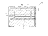
13s,13s,13t 第1の絶縁層
14,14a,14b 第2の絶縁層
14s 第1部分
14t 第2部分
14x,14y 第1部分
14z 第2部分
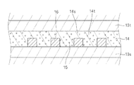
15 空孔
16 配線電極
17 配線電極
18 ビア導体
20,31,32,33 外部電極
36 配線電極
43 第1の絶縁層
44 第2の絶縁層
Claims (6)
- 第1の絶縁層と、
前記第1の絶縁層に接して配置された第2の絶縁層と、
前記第2の絶縁層のみに埋設された配線電極と、
前記第2の絶縁層に関して前記第1の絶縁層とは反対側において前記第2の絶縁層に接して配置された他の絶縁層と、
を備え、
前記第1の絶縁層及び他の絶縁層は、セラミックグリーンシートが焼結してなり、
前記第2の絶縁層は、セラミックペーストが焼結してなり、空孔が形成され、
前記第2の絶縁層は、積層方向から透視したときに前記配線電極に重なる第1部分と、該第1部分以外の第2部分とからなり、
前記第1部分の空孔含有率が、前記第2部分の空孔含有率よりも低いことを特徴とする、セラミック多層基板。 - 前記配線電極の厚みが、前記第2の絶縁層の厚みの半分以上であることを特徴とする、請求項1に記載のセラミック多層基板。
- 第1の絶縁層と、
前記第1の絶縁層に接して配置された第2の絶縁層と、
前記第1の絶縁層に接して配置され、前記第2の絶縁層のみに埋設された配線電極と、
前記第2の絶縁層に関して前記第1の絶縁層とは反対側において前記第2の絶縁層に接して配置された他の絶縁層と、
を備え、
前記第1の絶縁層及び他の絶縁層は、セラミックグリーンシートが焼結してなり、
前記第2の絶縁層は、セラミックペーストが焼結してなり、空孔が形成され、
前記第2の絶縁層は、積層方向から透視したときに前記配線電極に重なる第1部分と、該第1部分以外の第2部分とからなり、
前記第1部分の空孔含有率が、前記第2部分の空孔含有率よりも低いことを特徴とする、セラミック多層基板。 - 第1の絶縁層と、
前記第1の絶縁層に接して配置された第2の絶縁層と、
その周囲全体が前記第2の絶縁層で覆われるように、前記第2の絶縁層に埋設された配線電極と、
前記第2の絶縁層に関して前記第1の絶縁層とは反対側において前記第2の絶縁層に接して配置された他の絶縁層と、
を備え、
前記第1の絶縁層及び他の絶縁層は、セラミックグリーンシートが焼結してなり、
前記第2の絶縁層は、セラミックペーストが焼結してなり、空孔が形成され、
前記第2の絶縁層は、積層方向から透視したときに前記配線電極に重なる第1部分と、該第1部分以外の第2部分とからなり、
前記第1部分の空孔含有率が、前記第2部分の空孔含有率よりも低いことを特徴とする、セラミック多層基板。 - 前記第2の絶縁層の空孔含有率が、0.1vol%以上、かつ30vol%以下であることを特徴とする、請求項1ないし4に記載のセラミック多層基板。
- 未焼成のセラミックグリーンシートを含む基材上に、配線電極を配置する、第1のステップと、
前記配線電極を覆うように、前記基材上にセラミックペーストを塗布する、第2のステップと、
少なくとも前記セラミックペースト上に未焼成のセラミックグリーンシートを含む他の基材を、前記他の基材が前記セラミックペーストに接するように圧着して、未焼成セラミック積層体を形成する、第3のステップと、
前記未焼成セラミック積層体を焼成して、前記セラミックグリーンシート及び前記セラミックペーストを焼結させる、第4のステップと、
を含み、
焼成済みの前記セラミック積層体により、前記セラミックグリーンシートが焼結した第1の絶縁層及び他の絶縁層の間に、前記セラミックペーストが焼結した第2の絶縁層が配置され、前記第2の絶縁層に空孔が形成されているセラミック多層基板を形成し、
前記第2の絶縁層は、積層方向から透視したときに前記配線電極に重なる第1部分と、該第1部分以外の第2部分とからなり、
前記第1部分の空孔含有率が、前記第2部分の空孔含有率よりも低いことを特徴とする、セラミック多層基板の製造方法。
Priority Applications (1)
| Application Number | Priority Date | Filing Date | Title |
|---|---|---|---|
| JP2007214083A JP5194635B2 (ja) | 2007-08-20 | 2007-08-20 | セラミック多層基板及びその製造方法 |
Applications Claiming Priority (1)
| Application Number | Priority Date | Filing Date | Title |
|---|---|---|---|
| JP2007214083A JP5194635B2 (ja) | 2007-08-20 | 2007-08-20 | セラミック多層基板及びその製造方法 |
Publications (2)
| Publication Number | Publication Date |
|---|---|
| JP2009049205A JP2009049205A (ja) | 2009-03-05 |
| JP5194635B2 true JP5194635B2 (ja) | 2013-05-08 |
Family
ID=40501157
Family Applications (1)
| Application Number | Title | Priority Date | Filing Date |
|---|---|---|---|
| JP2007214083A Active JP5194635B2 (ja) | 2007-08-20 | 2007-08-20 | セラミック多層基板及びその製造方法 |
Country Status (1)
| Country | Link |
|---|---|
| JP (1) | JP5194635B2 (ja) |
Families Citing this family (2)
| Publication number | Priority date | Publication date | Assignee | Title |
|---|---|---|---|---|
| JP6989292B2 (ja) * | 2017-05-29 | 2022-01-05 | 京セラ株式会社 | 電子素子実装用基板、電子装置および電子モジュール |
| WO2025070020A1 (ja) * | 2023-09-28 | 2025-04-03 | 京セラ株式会社 | 配線基板の製造方法 |
Family Cites Families (9)
| Publication number | Priority date | Publication date | Assignee | Title |
|---|---|---|---|---|
| JP3470812B2 (ja) * | 1992-02-05 | 2003-11-25 | 株式会社村田製作所 | セラミック積層電子部品の製造方法 |
| JP2001284819A (ja) * | 2000-03-30 | 2001-10-12 | Kyocera Corp | 積層回路基板 |
| JP4134693B2 (ja) * | 2002-11-20 | 2008-08-20 | 日立金属株式会社 | セラミック積層基板の製造方法 |
| JP2004235347A (ja) * | 2003-01-29 | 2004-08-19 | Kyocera Corp | 絶縁性セラミックスおよびそれを用いた多層セラミック基板 |
| JP2005085995A (ja) * | 2003-09-09 | 2005-03-31 | Ngk Spark Plug Co Ltd | セラミック基板の製造方法 |
| US7251120B2 (en) * | 2003-09-30 | 2007-07-31 | Murata Manufacturing Co., Ltd. | Monolithic ceramic electronic component and method for making the same |
| JP2005154207A (ja) * | 2003-11-26 | 2005-06-16 | Kyocera Corp | グリーンシート、積層成形体、積層基板及びその製造方法 |
| JP2005243931A (ja) * | 2004-02-26 | 2005-09-08 | Kyocera Corp | ガラスセラミック多層基板、その配線基板及びそれ等の製造方法 |
| JP2007201272A (ja) * | 2006-01-27 | 2007-08-09 | Kyocera Corp | 配線基板の製造方法 |
-
2007
- 2007-08-20 JP JP2007214083A patent/JP5194635B2/ja active Active
Also Published As
| Publication number | Publication date |
|---|---|
| JP2009049205A (ja) | 2009-03-05 |
Similar Documents
| Publication | Publication Date | Title |
|---|---|---|
| JP5104761B2 (ja) | セラミック基板およびその製造方法 | |
| TWI436387B (zh) | Laminated ceramic electronic parts and manufacturing method thereof | |
| JPWO2017154692A1 (ja) | 複合基板及び複合基板の製造方法 | |
| JP2021168413A (ja) | 積層型電子部品 | |
| JP2010045209A (ja) | 積層セラミック電子部品の製造方法 | |
| JP7309666B2 (ja) | 多層セラミック基板及び電子装置 | |
| JP5194635B2 (ja) | セラミック多層基板及びその製造方法 | |
| JP4688460B2 (ja) | コンデンサ内蔵ガラスセラミック多層配線基板 | |
| JP4276642B2 (ja) | 積層型セラミック電子部品 | |
| JP5110420B2 (ja) | Ag粉末、導体ペースト及び多層セラミック基板とその製造方法 | |
| CN117316618A (zh) | 线圈部件的制造方法以及线圈部件 | |
| JP4844317B2 (ja) | セラミック電子部品およびその製造方法 | |
| JP2010045212A (ja) | 積層セラミック電子部品及びその製造方法 | |
| JP5110419B2 (ja) | Ag粉末、導体ペースト及び多層セラミック基板とその製造方法 | |
| JP2004273426A (ja) | 導電ペーストおよびそれを用いたセラミック多層基板 | |
| JP4658465B2 (ja) | コンデンサ内蔵ガラスセラミック多層配線基板 | |
| JP5230565B2 (ja) | 配線基板 | |
| JP6455633B2 (ja) | 多層セラミック基板及び電子装置 | |
| JP4416342B2 (ja) | 回路基板およびその製造方法 | |
| JP4738166B2 (ja) | 配線基板およびその製造方法 | |
| JP4817855B2 (ja) | コンデンサ内蔵配線基板およびその製造方法 | |
| JP2007173651A (ja) | 積層セラミックコンデンサ、コンデンサ内蔵多層配線基板、および積層電子装置 | |
| JP4530864B2 (ja) | コンデンサ内蔵配線基板 | |
| JP5718167B2 (ja) | 電子部品 | |
| JP2008037675A (ja) | 低温焼結セラミック組成物、セラミック基板およびその製造方法、ならびに電子部品 |
Legal Events
| Date | Code | Title | Description |
|---|---|---|---|
| A621 | Written request for application examination |
Free format text: JAPANESE INTERMEDIATE CODE: A621 Effective date: 20100507 |
|
| A977 | Report on retrieval |
Free format text: JAPANESE INTERMEDIATE CODE: A971007 Effective date: 20111215 |
|
| A131 | Notification of reasons for refusal |
Free format text: JAPANESE INTERMEDIATE CODE: A131 Effective date: 20111220 |
|
| A521 | Written amendment |
Free format text: JAPANESE INTERMEDIATE CODE: A523 Effective date: 20120215 |
|
| A131 | Notification of reasons for refusal |
Free format text: JAPANESE INTERMEDIATE CODE: A131 Effective date: 20120607 |
|
| A521 | Written amendment |
Free format text: JAPANESE INTERMEDIATE CODE: A523 Effective date: 20120802 |
|
| TRDD | Decision of grant or rejection written | ||
| A01 | Written decision to grant a patent or to grant a registration (utility model) |
Free format text: JAPANESE INTERMEDIATE CODE: A01 Effective date: 20130108 |
|
| A61 | First payment of annual fees (during grant procedure) |
Free format text: JAPANESE INTERMEDIATE CODE: A61 Effective date: 20130121 |
|
| FPAY | Renewal fee payment (event date is renewal date of database) |
Free format text: PAYMENT UNTIL: 20160215 Year of fee payment: 3 |
|
| R150 | Certificate of patent or registration of utility model |
Ref document number: 5194635 Country of ref document: JP Free format text: JAPANESE INTERMEDIATE CODE: R150 Free format text: JAPANESE INTERMEDIATE CODE: R150 |