JP5194635B2 - Ceramic multilayer substrate and manufacturing method thereof - Google Patents
Ceramic multilayer substrate and manufacturing method thereof Download PDFInfo
- Publication number
- JP5194635B2 JP5194635B2 JP2007214083A JP2007214083A JP5194635B2 JP 5194635 B2 JP5194635 B2 JP 5194635B2 JP 2007214083 A JP2007214083 A JP 2007214083A JP 2007214083 A JP2007214083 A JP 2007214083A JP 5194635 B2 JP5194635 B2 JP 5194635B2
- Authority
- JP
- Japan
- Prior art keywords
- insulating layer
- ceramic
- wiring electrode
- green sheet
- multilayer substrate
- Prior art date
- Legal status (The legal status is an assumption and is not a legal conclusion. Google has not performed a legal analysis and makes no representation as to the accuracy of the status listed.)
- Active
Links
- 239000000919 ceramic Substances 0.000 title claims description 268
- 239000000758 substrate Substances 0.000 title claims description 99
- 238000004519 manufacturing process Methods 0.000 title claims description 15
- 239000011800 void material Substances 0.000 claims description 37
- 239000011148 porous material Substances 0.000 claims description 21
- 238000010304 firing Methods 0.000 claims description 19
- 238000005245 sintering Methods 0.000 claims description 18
- 238000003825 pressing Methods 0.000 claims description 2
- 239000010410 layer Substances 0.000 description 166
- 238000000034 method Methods 0.000 description 32
- 239000000843 powder Substances 0.000 description 30
- 229910010293 ceramic material Inorganic materials 0.000 description 21
- 239000004020 conductor Substances 0.000 description 16
- 238000003780 insertion Methods 0.000 description 13
- 230000037431 insertion Effects 0.000 description 13
- 239000000463 material Substances 0.000 description 13
- 230000008569 process Effects 0.000 description 13
- 238000007639 printing Methods 0.000 description 12
- 238000012545 processing Methods 0.000 description 9
- 239000002002 slurry Substances 0.000 description 9
- 238000012360 testing method Methods 0.000 description 9
- 239000011229 interlayer Substances 0.000 description 8
- 229910052751 metal Inorganic materials 0.000 description 8
- 239000002184 metal Substances 0.000 description 8
- 238000007747 plating Methods 0.000 description 8
- 230000035882 stress Effects 0.000 description 8
- 229910018072 Al 2 O 3 Inorganic materials 0.000 description 7
- 229910004298 SiO 2 Inorganic materials 0.000 description 7
- 239000011230 binding agent Substances 0.000 description 7
- 238000011156 evaluation Methods 0.000 description 7
- 239000003960 organic solvent Substances 0.000 description 7
- 238000009413 insulation Methods 0.000 description 6
- 239000000203 mixture Substances 0.000 description 6
- 239000002245 particle Substances 0.000 description 6
- 239000004014 plasticizer Substances 0.000 description 6
- 239000012298 atmosphere Substances 0.000 description 5
- 230000007547 defect Effects 0.000 description 5
- 229910010413 TiO 2 Inorganic materials 0.000 description 4
- MCMNRKCIXSYSNV-UHFFFAOYSA-N Zirconium dioxide Chemical compound O=[Zr]=O MCMNRKCIXSYSNV-UHFFFAOYSA-N 0.000 description 4
- 239000002585 base Substances 0.000 description 4
- 239000003990 capacitor Substances 0.000 description 4
- 230000008878 coupling Effects 0.000 description 4
- 238000010168 coupling process Methods 0.000 description 4
- 238000005859 coupling reaction Methods 0.000 description 4
- 230000007423 decrease Effects 0.000 description 4
- 239000011521 glass Substances 0.000 description 4
- 238000010030 laminating Methods 0.000 description 4
- 238000012986 modification Methods 0.000 description 4
- 230000004048 modification Effects 0.000 description 4
- 239000001856 Ethyl cellulose Substances 0.000 description 3
- ZZSNKZQZMQGXPY-UHFFFAOYSA-N Ethyl cellulose Chemical compound CCOCC1OC(OC)C(OCC)C(OCC)C1OC1C(O)C(O)C(OC)C(CO)O1 ZZSNKZQZMQGXPY-UHFFFAOYSA-N 0.000 description 3
- YXFVVABEGXRONW-UHFFFAOYSA-N Toluene Chemical compound CC1=CC=CC=C1 YXFVVABEGXRONW-UHFFFAOYSA-N 0.000 description 3
- WUOACPNHFRMFPN-UHFFFAOYSA-N alpha-terpineol Chemical compound CC1=CCC(C(C)(C)O)CC1 WUOACPNHFRMFPN-UHFFFAOYSA-N 0.000 description 3
- 229910052782 aluminium Inorganic materials 0.000 description 3
- 239000000292 calcium oxide Substances 0.000 description 3
- 239000003795 chemical substances by application Substances 0.000 description 3
- 230000008602 contraction Effects 0.000 description 3
- SQIFACVGCPWBQZ-UHFFFAOYSA-N delta-terpineol Natural products CC(C)(O)C1CCC(=C)CC1 SQIFACVGCPWBQZ-UHFFFAOYSA-N 0.000 description 3
- 239000002270 dispersing agent Substances 0.000 description 3
- 238000007606 doctor blade method Methods 0.000 description 3
- 229920001249 ethyl cellulose Polymers 0.000 description 3
- 235000019325 ethyl cellulose Nutrition 0.000 description 3
- 238000010438 heat treatment Methods 0.000 description 3
- 239000012212 insulator Substances 0.000 description 3
- 229920005989 resin Polymers 0.000 description 3
- 239000011347 resin Substances 0.000 description 3
- 229940116411 terpineol Drugs 0.000 description 3
- DAFHKNAQFPVRKR-UHFFFAOYSA-N (3-hydroxy-2,2,4-trimethylpentyl) 2-methylpropanoate Chemical compound CC(C)C(O)C(C)(C)COC(=O)C(C)C DAFHKNAQFPVRKR-UHFFFAOYSA-N 0.000 description 2
- OAYXUHPQHDHDDZ-UHFFFAOYSA-N 2-(2-butoxyethoxy)ethanol Chemical compound CCCCOCCOCCO OAYXUHPQHDHDDZ-UHFFFAOYSA-N 0.000 description 2
- VXQBJTKSVGFQOL-UHFFFAOYSA-N 2-(2-butoxyethoxy)ethyl acetate Chemical compound CCCCOCCOCCOC(C)=O VXQBJTKSVGFQOL-UHFFFAOYSA-N 0.000 description 2
- 229920000178 Acrylic resin Polymers 0.000 description 2
- 239000004925 Acrylic resin Substances 0.000 description 2
- ODINCKMPIJJUCX-UHFFFAOYSA-N Calcium oxide Chemical compound [Ca]=O ODINCKMPIJJUCX-UHFFFAOYSA-N 0.000 description 2
- 150000001298 alcohols Chemical class 0.000 description 2
- PNEYBMLMFCGWSK-UHFFFAOYSA-N aluminium oxide Inorganic materials [O-2].[O-2].[O-2].[Al+3].[Al+3] PNEYBMLMFCGWSK-UHFFFAOYSA-N 0.000 description 2
- QVGXLLKOCUKJST-UHFFFAOYSA-N atomic oxygen Chemical compound [O] QVGXLLKOCUKJST-UHFFFAOYSA-N 0.000 description 2
- 229910002113 barium titanate Inorganic materials 0.000 description 2
- JRPBQTZRNDNNOP-UHFFFAOYSA-N barium titanate Chemical compound [Ba+2].[Ba+2].[O-][Ti]([O-])([O-])[O-] JRPBQTZRNDNNOP-UHFFFAOYSA-N 0.000 description 2
- 230000015556 catabolic process Effects 0.000 description 2
- 238000001816 cooling Methods 0.000 description 2
- 229910052802 copper Inorganic materials 0.000 description 2
- DOIRQSBPFJWKBE-UHFFFAOYSA-N dibutyl phthalate Chemical compound CCCCOC(=O)C1=CC=CC=C1C(=O)OCCCC DOIRQSBPFJWKBE-UHFFFAOYSA-N 0.000 description 2
- 239000003989 dielectric material Substances 0.000 description 2
- 238000001035 drying Methods 0.000 description 2
- 239000003792 electrolyte Substances 0.000 description 2
- 239000006260 foam Substances 0.000 description 2
- 239000012535 impurity Substances 0.000 description 2
- 238000004898 kneading Methods 0.000 description 2
- 239000000696 magnetic material Substances 0.000 description 2
- UODXCYZDMHPIJE-UHFFFAOYSA-N menthanol Chemical compound CC1CCC(C(C)(C)O)CC1 UODXCYZDMHPIJE-UHFFFAOYSA-N 0.000 description 2
- 229910021645 metal ion Inorganic materials 0.000 description 2
- 239000000113 methacrylic resin Substances 0.000 description 2
- 238000013508 migration Methods 0.000 description 2
- 230000005012 migration Effects 0.000 description 2
- 238000002156 mixing Methods 0.000 description 2
- PLDDOISOJJCEMH-UHFFFAOYSA-N neodymium(3+);oxygen(2-) Chemical compound [O-2].[O-2].[O-2].[Nd+3].[Nd+3] PLDDOISOJJCEMH-UHFFFAOYSA-N 0.000 description 2
- 229910052760 oxygen Inorganic materials 0.000 description 2
- 239000001301 oxygen Substances 0.000 description 2
- 229920002037 poly(vinyl butyral) polymer Polymers 0.000 description 2
- 238000004080 punching Methods 0.000 description 2
- 230000035939 shock Effects 0.000 description 2
- 229910052709 silver Inorganic materials 0.000 description 2
- 239000002904 solvent Substances 0.000 description 2
- 238000003756 stirring Methods 0.000 description 2
- 229910000859 α-Fe Inorganic materials 0.000 description 2
- HBNHCGDYYBMKJN-UHFFFAOYSA-N 2-(4-methylcyclohexyl)propan-2-yl acetate Chemical compound CC1CCC(C(C)(C)OC(C)=O)CC1 HBNHCGDYYBMKJN-UHFFFAOYSA-N 0.000 description 1
- GWEVSGVZZGPLCZ-UHFFFAOYSA-N Titan oxide Chemical compound O=[Ti]=O GWEVSGVZZGPLCZ-UHFFFAOYSA-N 0.000 description 1
- MLBISOBTPLLTLK-UHFFFAOYSA-N [O-2].[O-2].[Ti+4].[Nd+3] Chemical compound [O-2].[O-2].[Ti+4].[Nd+3] MLBISOBTPLLTLK-UHFFFAOYSA-N 0.000 description 1
- NIXOWILDQLNWCW-UHFFFAOYSA-N acrylic acid group Chemical group C(C=C)(=O)O NIXOWILDQLNWCW-UHFFFAOYSA-N 0.000 description 1
- 239000012190 activator Substances 0.000 description 1
- 239000000654 additive Substances 0.000 description 1
- 230000000996 additive effect Effects 0.000 description 1
- 238000004220 aggregation Methods 0.000 description 1
- 230000002776 aggregation Effects 0.000 description 1
- 239000003513 alkali Substances 0.000 description 1
- 229920000180 alkyd Polymers 0.000 description 1
- 230000015572 biosynthetic process Effects 0.000 description 1
- 239000005388 borosilicate glass Substances 0.000 description 1
- 235000012255 calcium oxide Nutrition 0.000 description 1
- 239000011362 coarse particle Substances 0.000 description 1
- 239000012141 concentrate Substances 0.000 description 1
- 238000005520 cutting process Methods 0.000 description 1
- 230000002950 deficient Effects 0.000 description 1
- 238000013461 design Methods 0.000 description 1
- 230000000694 effects Effects 0.000 description 1
- 230000005672 electromagnetic field Effects 0.000 description 1
- 239000003822 epoxy resin Substances 0.000 description 1
- 229910052737 gold Inorganic materials 0.000 description 1
- 230000002706 hydrostatic effect Effects 0.000 description 1
- -1 isopropylene alcohol Chemical compound 0.000 description 1
- 238000003475 lamination Methods 0.000 description 1
- 238000005259 measurement Methods 0.000 description 1
- 150000002739 metals Chemical class 0.000 description 1
- 229910052759 nickel Inorganic materials 0.000 description 1
- 229920000647 polyepoxide Polymers 0.000 description 1
- 239000002994 raw material Substances 0.000 description 1
- 230000009467 reduction Effects 0.000 description 1
- 230000002040 relaxant effect Effects 0.000 description 1
- 238000007790 scraping Methods 0.000 description 1
- 238000007650 screen-printing Methods 0.000 description 1
- 239000005368 silicate glass Substances 0.000 description 1
- 229910000679 solder Inorganic materials 0.000 description 1
- 239000007787 solid Substances 0.000 description 1
- 238000004528 spin coating Methods 0.000 description 1
- 238000005507 spraying Methods 0.000 description 1
- 239000004094 surface-active agent Substances 0.000 description 1
- 230000008646 thermal stress Effects 0.000 description 1
- OGIDPMRJRNCKJF-UHFFFAOYSA-N titanium oxide Inorganic materials [Ti]=O OGIDPMRJRNCKJF-UHFFFAOYSA-N 0.000 description 1
- 229920002554 vinyl polymer Polymers 0.000 description 1
Images


Landscapes
- Production Of Multi-Layered Print Wiring Board (AREA)
Description
本発明はセラミック多層基板及びその製造方法に関し、詳しくは、内部に配線電極を備えたセラミック多層基板の構造とその製造方法に関する。 The present invention relates to a ceramic multilayer substrate and a method for manufacturing the same, and more particularly to a structure of a ceramic multilayer substrate having wiring electrodes therein and a method for manufacturing the same.
セラミック多層基板を備えた積層電子部品は、複数の絶縁層の間に、抵抗、キャパシタ、インダクタなどの回路素子を構成する配線電極が配置されている。 In a multilayer electronic component including a ceramic multilayer substrate, wiring electrodes constituting circuit elements such as resistors, capacitors, and inductors are disposed between a plurality of insulating layers.
このような積層電子部品を製造するために、セラミックグリーンシート上に配線電極を形成し、その上に別のグリーンシートを積層すると、配線電極近傍で空隙が発生したり、セラミックグリーンシート表面が平坦にならないことがある。これに対しては、配線電極の形状に対応した凹部をグリーンシートに形成し、その凹部に配線電極を形成することにより、配線電極による段差を解消すれば、改善できる。 In order to manufacture such a multilayer electronic component, when a wiring electrode is formed on a ceramic green sheet and another green sheet is laminated on the ceramic green sheet, voids are generated in the vicinity of the wiring electrode or the surface of the ceramic green sheet is flat. It may not be. This can be improved by forming a recess corresponding to the shape of the wiring electrode in the green sheet and forming the wiring electrode in the recess to eliminate the step caused by the wiring electrode.
例えば特許文献1には、図9の断面図に示すように、グリーンシート80にレーザ加工で形成した凹部内に、配線電極82を配置することが提案されている。
しかし、特許文献1の方法で製造する場合には、高価なレーザ装置が必要になり、また凹部を加工するための工程が必要になる。 However, when manufacturing by the method of patent document 1, an expensive laser apparatus is needed and the process for processing a recessed part is needed.
一方、積層電子部品の製造方法として、上述のシート積層法のほかに、配線電極及び絶縁体部分をペースト等の印刷により形成する印刷方法も知られている。しかし、印刷法を用いた場合、絶縁体部分用のセラミックペーストは、配線電極用のペーストに比べ、柔らかく、かつ粘性も低いため、絶縁体部分が配線電極よりも低くなり、配線電極部が凸状に突出し、積層数が増加すると、積層体表面の平坦性が悪くなるという問題があった。 On the other hand, as a method for manufacturing a laminated electronic component, in addition to the above-described sheet laminating method, a printing method is also known in which a wiring electrode and an insulator portion are formed by printing a paste or the like. However, when the printing method is used, the ceramic paste for the insulator part is softer and less viscous than the paste for the wiring electrode, so the insulator part is lower than the wiring electrode and the wiring electrode part is convex. When the number of stacked layers increases, the flatness of the surface of the stacked body deteriorates.
本発明は、かかる実情に鑑み、シート積層法と印刷法による問題を改善することを目的とし、セラミック多層基板の内部に配線電極を設けても、低コストかつ簡単な工程で、セラミック多層基板の平坦性を確保することができる、セラミック多層基板の構造及び製造方法を提供しようとするものである。 In view of such circumstances, the present invention aims to improve the problems caused by the sheet lamination method and the printing method, and even if a wiring electrode is provided inside the ceramic multilayer substrate, the ceramic multilayer substrate can be manufactured at a low cost and with a simple process. An object of the present invention is to provide a structure and manufacturing method of a ceramic multilayer substrate that can ensure flatness.
本発明は、上記課題を解決するために、以下のように構成したセラミック多層基板を提供する。 In order to solve the above-described problems, the present invention provides a ceramic multilayer substrate configured as follows.
セラミック多層基板は、(a)第1の絶縁層と、(b)前記第1の絶縁層に接して配置された第2の絶縁層と、(c)前記第2の絶縁層のみに埋設された配線電極と、(d)前記第2の絶縁層に関して前記第1の絶縁層とは反対側において前記第2の絶縁層に接して配置された他の絶縁層とを備える。前記第1の絶縁層及び他の絶縁層は、セラミックグリーンシートが焼結してなる。前記第2の絶縁層は、セラミックペーストが焼結してなり、空孔が形成されている。前記第2の絶縁層は、積層方向から透視したときに前記配線電極に重なる第1部分と、該第1部分以外の第2部分とからなる。前記第1部分の空孔含有率が、前記第2部分の空孔含有率よりも低い。好ましくは、前記配線電極の厚みが、前記第2の絶縁層の厚みの半分以上である。 The ceramic multilayer substrate is embedded in (a) a first insulating layer, (b) a second insulating layer disposed in contact with the first insulating layer, and (c) only the second insulating layer. And (d) another insulating layer disposed in contact with the second insulating layer on the side opposite to the first insulating layer with respect to the second insulating layer. The first insulating layer and the other insulating layers are formed by sintering a ceramic green sheet. The second insulating layer is formed by sintering a ceramic paste to form pores. The second insulating layer includes a first portion that overlaps the wiring electrode when seen through from the stacking direction, and a second portion other than the first portion. The void content of the first portion is lower than the void content of the second portion. Preferably, the thickness of the wiring electrode is not less than half of the thickness of the second insulating layer.
上記構成によれば、例えば、第1の絶縁層を形成するためのセラミックグリーンシート上に、配線電極を、第1の絶縁層に接するように、又は第1の絶縁層から離れるように配置し、配線電極が第1の絶縁層には埋設されていない状態で、第2の絶縁層を形成するためのセラミックぺーストを、配線電極を覆うように配置することにより、セラミックグリーンシートにレーザ加工で凹部を形成して該凹部に配線電極を配置する場合よりも低コストかつ簡単な工程で、セラミック多層基板の内部に配線電極を設けることができる。 According to the above configuration, for example, the wiring electrode is disposed on the ceramic green sheet for forming the first insulating layer so as to be in contact with the first insulating layer or away from the first insulating layer. In a state where the wiring electrode is not embedded in the first insulating layer, a ceramic paste for forming the second insulating layer is disposed so as to cover the wiring electrode, so that laser processing is performed on the ceramic green sheet. Thus, the wiring electrodes can be provided inside the ceramic multilayer substrate by a simpler process at a lower cost than when forming the recesses and disposing the wiring electrodes in the recesses.
また、セラミックグリーンシートとセラミックペーストを併用して絶縁層を形成することで、セラミックペーストだけで絶縁層を形成する場合よりも、セラミック多層基板の平坦性を確保することができる。 Further, by forming the insulating layer by using the ceramic green sheet and the ceramic paste in combination, the flatness of the ceramic multilayer substrate can be ensured as compared with the case where the insulating layer is formed only with the ceramic paste.
第2の絶縁層には、第2の絶縁層を形成するためのセラミックぺーストに含まれる泡によって、空孔が形成される。空孔は、絶縁性を低下させる原因となる。配線電極の厚みが第2の絶縁層の厚みの半分以上であれば、配線電極の上又は下の第2の絶縁層が薄くなるため、この部分の空孔含有率が、第2の絶縁層の他の部分の空孔含有率よりも小さくなる。そのため、第2の絶縁層の空孔含有率が一定である場合(例えば、セラミックグリーンシートにレーザ加工で凹部を形成した場合)に比べると、絶縁性を向上させることができる。 In the second insulating layer, pores are formed by bubbles contained in the ceramic paste for forming the second insulating layer. A void | hole becomes a cause which reduces insulation. If the thickness of the wiring electrode is more than half of the thickness of the second insulating layer, the second insulating layer above or below the wiring electrode is thinned. It becomes smaller than the vacancy content of other parts. Therefore, the insulating property can be improved as compared with the case where the void content of the second insulating layer is constant (for example, when the concave portion is formed by laser processing on the ceramic green sheet).
また、本発明は、上記課題を解決するために、以下のように構成した他のセラミック多層基板を提供する。 In order to solve the above-mentioned problems, the present invention provides another ceramic multilayer substrate configured as follows.
セラミック多層基板は、(a)第1の絶縁層と、(b)前記第1の絶縁層に接して配置された第2の絶縁層と、(c)前記第1の絶縁層に接して配置され、前記第2の絶縁層のみに埋設された配線電極と、(d)前記第2の絶縁層に関して前記第1の絶縁層とは反対側において前記第2の絶縁層に接して配置された他の絶縁層とを備える。前記第1の絶縁層及び他の絶縁層は、セラミックグリーンシートが焼結してなる。前記第2の絶縁層は、セラミックペーストが焼結してなり、空孔が形成されている。前記第2の絶縁層は、積層方向から透視したときに前記配線電極に重なる第1部分と、該第1部分以外の第2部分とからなる。前記第1部分の空孔含有率が、前記第2部分の空孔含有率よりも低い。 The ceramic multilayer substrate includes: (a) a first insulating layer; (b) a second insulating layer disposed in contact with the first insulating layer; and (c) disposed in contact with the first insulating layer. A wiring electrode embedded only in the second insulating layer , and (d) disposed in contact with the second insulating layer on the side opposite to the first insulating layer with respect to the second insulating layer. And another insulating layer . The first insulating layer and the other insulating layers are formed by sintering a ceramic green sheet. The second insulating layer, Ri ceramic paste Na sintered, that have pores formed. The second insulating layer includes a first portion that overlaps the wiring electrode when seen through from the stacking direction, and a second portion other than the first portion. The void content of the first portion is lower than the void content of the second portion.
上記構成によれば、例えば、第1の絶縁層を形成するためのセラミックグリーンシート上に、配線電極を、第1の絶縁層に接するように配置し、配線電極が第1の絶縁層には埋設されていない状態で、第2の絶縁層を形成するためのセラミックぺーストを、配線電極を覆うように配置することにより、セラミックグリーンシートにレーザ加工で凹部を形成して該凹部に配線電極を配置する場合よりも低コストかつ簡単な工程で、セラミック多層基板の内部に配線電極を設けることができる。 According to the above configuration, for example, the wiring electrode is disposed on the ceramic green sheet for forming the first insulating layer so as to be in contact with the first insulating layer, and the wiring electrode is disposed on the first insulating layer. A ceramic paste for forming the second insulating layer is disposed so as to cover the wiring electrode in a state where it is not buried, so that a concave portion is formed in the ceramic green sheet by laser processing, and the wiring electrode is formed in the concave portion. Wiring electrodes can be provided inside the ceramic multilayer substrate by a lower cost and simpler process than in the case of arranging the electrodes.
また、セラミックグリーンシートとセラミックペーストを併用して絶縁層を形成することで、セラミックペーストだけで絶縁層を形成する場合よりも、セラミック多層基板の平坦性を確保することができる。 Further, by forming the insulating layer by using the ceramic green sheet and the ceramic paste in combination, the flatness of the ceramic multilayer substrate can be ensured as compared with the case where the insulating layer is formed only with the ceramic paste.
第2の絶縁層には、第2の絶縁層を形成するためのセラミックぺーストに含まれる泡によって、空孔が形成される。空孔は、絶縁性を低下させる原因となる。第2の絶縁層の第1部分の空孔含有率が、第2の絶縁層の第2部分の空孔含有率よりも低いと、第2の絶縁層の空孔含有率が一定である場合(例えば、セラミックグリーンシートにレーザ加工で凹部を形成した場合)に比べると、絶縁性を向上させることができる。 In the second insulating layer, pores are formed by bubbles contained in the ceramic paste for forming the second insulating layer. A void | hole becomes a cause which reduces insulation. When the vacancy content of the first insulating layer is lower than the vacancy content of the second insulating layer, the second insulating layer has a constant vacancy content. Compared to (for example, when a concave portion is formed by laser processing on a ceramic green sheet), the insulating property can be improved.
また、本発明は、上記課題を解決するために、以下のように構成したさらに別のセラミック多層基板を提供する。 Moreover, in order to solve the said subject, this invention provides the another ceramic multilayer substrate comprised as follows.
セラミック多層基板は、(a)第1の絶縁層と、(b)前記第1の絶縁層に接して配置された第2の絶縁層と、(c)その周囲全体が前記第2の絶縁層で覆われるように、前記第2の絶縁層に埋設された配線電極と、(d)前記第2の絶縁層に関して前記第1の絶縁層とは反対側において前記第2の絶縁層に接して配置された他の絶縁層とを備える。前記第1の絶縁層及び他の絶縁層は、セラミックグリーンシートが焼結してなる。前記第2の絶縁層は、セラミックペーストが焼結してなり、空孔が形成されている。前記第2の絶縁層は、積層方向から透視したときに前記配線電極に重なる第1部分と、該第1部分以外の第2部分とからなる。前記第1部分の空孔含有率が、前記第2部分の空孔含有率よりも低い。 The ceramic multilayer substrate includes: (a) a first insulating layer; (b) a second insulating layer disposed in contact with the first insulating layer; and (c) an entire periphery of the second insulating layer. A wiring electrode embedded in the second insulating layer so as to be covered with , and (d) in contact with the second insulating layer on the opposite side of the first insulating layer with respect to the second insulating layer. Another insulating layer disposed . The first insulating layer and the other insulating layers are formed by sintering a ceramic green sheet. The second insulating layer, Ri ceramic paste Na sintered, that have pores formed. The second insulating layer includes a first portion that overlaps the wiring electrode when seen through from the stacking direction, and a second portion other than the first portion. The void content of the first portion is lower than the void content of the second portion.
上記構成によれば、例えば、第1の絶縁層を形成するためのセラミックグリーンシート上に、第2の絶縁層の一部を形成するためのセラミックぺーストを配置し、このセラミックペースト上に配線電極を配置し、配線電極が第1の絶縁層から離れている状態、すなわち第1の絶縁層には埋設されていない状態で、第2の絶縁層の残りの部分を形成するためのセラミックぺーストを、配線電極を覆うように配置することにより、セラミックグリーンシートにレーザ加工で凹部を形成して該凹部に配線電極を配置する場合よりも低コストかつ簡単な工程で、セラミック多層基板の内部に配線電極を設けることができる。 According to the above configuration, for example, the ceramic paste for forming a part of the second insulating layer is disposed on the ceramic green sheet for forming the first insulating layer, and the wiring is formed on the ceramic paste. A ceramic page for forming the remaining portion of the second insulating layer in a state where the electrode is disposed and the wiring electrode is separated from the first insulating layer, that is, not embedded in the first insulating layer. By disposing the strike so as to cover the wiring electrode, the inside of the ceramic multilayer substrate can be manufactured at a lower cost and with a simpler process than the case where a recess is formed in the ceramic green sheet by laser processing and the wiring electrode is placed in the recess. Wiring electrodes can be provided on the substrate.
また、セラミックグリーンシートとセラミックペーストを併用して絶縁層を形成することで、セラミックペーストだけで絶縁層を形成する場合よりも、セラミック多層基板の平坦性を確保することができる。 Further, by forming the insulating layer by using the ceramic green sheet and the ceramic paste in combination, the flatness of the ceramic multilayer substrate can be ensured as compared with the case where the insulating layer is formed only with the ceramic paste.
第2の絶縁層には、第2の絶縁層を形成するためのセラミックぺーストに含まれる泡によって、空孔が形成される。空孔は、絶縁性を低下させる原因となる。第2の絶縁層の第1部分の空孔含有率が、第2の絶縁層の第2部分の空孔含有率よりも低いと、第2の絶縁層の空孔含有率が一定である場合(例えば、セラミックグリーンシートにレーザ加工で凹部を形成した場合)に比べると、絶縁性を向上させることができる。 In the second insulating layer, pores are formed by bubbles contained in the ceramic paste for forming the second insulating layer. A void | hole becomes a cause which reduces insulation. When the vacancy content of the first insulating layer is lower than the vacancy content of the second insulating layer, the second insulating layer has a constant vacancy content. Compared to (for example, when a concave portion is formed by laser processing on a ceramic green sheet), the insulating property can be improved.
好ましくは、上記各構成において、前記第2の絶縁層の空孔含有率が、0.1vol%以上、かつ30vol%以下である。 Preferably, in each of the above structures, the void content of the second insulating layer is not less than 0.1 vol% and not more than 30 vol%.
第2の絶縁層の空孔含有率が0.1vol%以上であると、第2の絶縁層に発生する応力を緩和する効果が十分になる。第2の絶縁層の空孔含有率が30vol%以下であると、めっき工程でめっき液が基板内部に侵入しないので、空孔に残存しためっき液によるマイグレーションや、耐電圧の低下を引き起こす絶縁破壊が起こりにくい。 When the void content of the second insulating layer is 0.1 vol% or more, the effect of relaxing the stress generated in the second insulating layer is sufficient. When the void content of the second insulating layer is 30 vol% or less, the plating solution does not enter the substrate during the plating process, and therefore, the dielectric breakdown causes migration due to the plating solution remaining in the holes and a decrease in withstand voltage. Is unlikely to occur.
また、本発明は、上記課題を解決するために、以下のように構成したセラミック多層基板の製造方法を提供する。 Moreover, in order to solve the said subject, this invention provides the manufacturing method of the ceramic multilayer substrate comprised as follows.
セラミック多層基板の製造方法は、(1)未焼成のセラミックグリーンシートを含む基材上に、配線電極を配置する、第1のステップと、(2)前記配線電極を覆うように、前記基材上にセラミックペーストを塗布する、第2のステップと、(3)少なくとも前記セラミックペースト上に未焼成のセラミックグリーンシートを含む他の基材を、前記他の基材が前記セラミックペーストに接するように圧着して、未焼成セラミック積層体を形成する、第3のステップと、(4)前記未焼成セラミック積層体を焼成して、前記セラミックグリーンシート及び前記セラミックペーストを焼結させる、第4のステップとを含む。焼成済みの前記セラミック積層体により、前記セラミックグリーンシートが焼結した第1の絶縁層及び他の絶縁層の間に、前記セラミックペーストが焼結した第2の絶縁層が配置され、前記第2の絶縁層に空孔が形成されているセラミック多層基板を形成する。前記第2の絶縁層は、積層方向から透視したときに前記配線電極に重なる第1部分と、該第1部分以外の第2部分とからなる。前記第1部分の空孔含有率が、前記第2部分の空孔含有率よりも低い。 A method for producing a ceramic multilayer substrate includes: (1) a first step in which a wiring electrode is disposed on a base material including an unfired ceramic green sheet; and (2) the base material so as to cover the wiring electrode. A second step of applying a ceramic paste thereon; and (3) at least another substrate including an unfired ceramic green sheet on the ceramic paste, such that the other substrate contacts the ceramic paste. A third step of forming an unfired ceramic laminate by pressure bonding; and (4) a fourth step of firing the unfired ceramic laminate to sinter the ceramic green sheet and the ceramic paste. Including. A second insulating layer obtained by sintering the ceramic paste is disposed between the first insulating layer obtained by sintering the ceramic green sheet and another insulating layer by the sintered ceramic laminate, and the second insulating layer is provided. A ceramic multilayer substrate in which holes are formed in the insulating layer is formed. The second insulating layer includes a first portion that overlaps the wiring electrode when seen through from the stacking direction, and a second portion other than the first portion. The void content of the first portion is lower than the void content of the second portion.
上記第1のステップにおいて、セラミックグリーンシートのみからなる基材に電極を配置しても、セラミックグリーンシート上にセラミックペーストが塗布された基材を用い、この基材のセラミックペースト上に配線電極を配置してもよい。 In the first step, even if the electrode is disposed on the base material made of only the ceramic green sheet, the base material coated with the ceramic paste is used on the ceramic green sheet, and the wiring electrode is formed on the ceramic paste of the base material. You may arrange.
上記方法によれば、セラミックグリーンシートにレーザ加工で凹部を形成して該凹部に配線電極を配置する場合よりも低コストかつ簡単な工程で、セラミック多層基板の内部に配線電極を設けることができる。また、セラミックグリーンシートとセラミックペーストを併用して絶縁層を形成することで、セラミックペーストだけで絶縁層を形成する場合よりも、セラミック多層基板の平坦性を確保することができる。 According to the above method, the wiring electrode can be provided inside the ceramic multilayer substrate at a lower cost and with a simpler process than the case where the concave portion is formed by laser processing on the ceramic green sheet and the wiring electrode is disposed in the concave portion. . Further, by forming the insulating layer by using the ceramic green sheet and the ceramic paste in combination, the flatness of the ceramic multilayer substrate can be ensured as compared with the case where the insulating layer is formed only with the ceramic paste.
本発明によれば、セラミック多層基板の内部に配線電極を設けても、低コストかつ簡単な工程で、セラミック多層基板の平坦性を確保することができる。 According to the present invention, even if the wiring electrode is provided inside the ceramic multilayer substrate, the flatness of the ceramic multilayer substrate can be ensured by a low cost and simple process.
以下、本発明の実施の形態について、図1〜図8を参照しながら説明する。 Hereinafter, embodiments of the present invention will be described with reference to FIGS.
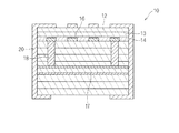
図1の断面図に概略構成を示すように、セラミック多層基板10は、セラミックの絶縁層が積層された基板本体12の内部に、配線電極16と、内部配線17と、層間接続ビア導体18とが配置され、基板本体12の側面に外部電極20が形成されている。
As shown schematically in the cross-sectional view of FIG. 1, the
配線電極16は、抵抗、キャパシタ、インダクタなどの回路素子を構成する。層間接続ビア導体18は、異なる層の配線電極16や内部配線17の間を電気的に接続する。配線電極16と、内部配線17と、層間接続ビア導体18とによって、任意の周波数の電気信号のみを取り出すための回路等が形成される。
The
外部電極20は、内部配線17を介して、基板本体12内の回路に電気的に接続されている。外部電極20は、セラミック多層基板10をプリント配線基板等の外部回路基板に実装する場合の電気的接続を行うために用いる。外部電極20は、必要に応じて、セラミック多層基板10を外部回路基板に実装するための位置合わせ用マークのために使用してもよい。
The
基板本体12の絶縁層は、セラミックグリーンシートが焼結してなる第1の絶縁層13と、セラミックペーストが焼結してなる第2の絶縁層14とを含む。配線電極16は、第2の絶縁層14のみに埋設されていている。
The insulating layer of the
図2の断面図に示すセラミック多層基板10aのように、配線電極16が埋設されている2層以上の第2の絶縁層14aを備えてもよい。
Like the
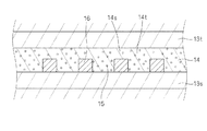
図3の要部断面図に示すように、第2の絶縁層14に埋設された配線電極16は、第1の絶縁層13sに接し、第2の絶縁層14は第1の絶縁層13s,13tに接している。
3, the
第2の絶縁層14には、第2の絶縁層14を形成するためのセラミックぺーストに含まれる泡によって、空孔15が形成されている。空孔15は、絶縁性を低下させる原因となる。
例えば、配線電極16の厚みが第2の絶縁層14の厚みの半分以上になるように形成されている。この場合、第2の絶縁層14となるセラミックペーストがスキージなどによって印刷され、配線電極16上のセラミックペースト中の泡は、他の部分のペースト中の泡よりも少なくなる。そのため、絶縁層14は、配線電極16の上の第1部分14s(積層方向から透視したときに配線電極16に重なる部分)の空孔含有率が、第2の絶縁層14の第1部分14s以外の第2部分14tの空孔含有率よりも小さくなる。このように第2の絶縁層14の第1部分14sの空孔含有率を小さくすることによって、第2の絶縁層14の空孔含有率が一定である場合に比べると、絶縁性を向上させることができる。
For example, the
第2の絶縁層14の空孔含有率が、上記のように第1部分14sと第2部分14tで異なれば、配線電極16の厚みが第2の絶縁層14の厚みの半分より小さい場合でも、同様に、絶縁性を向上させることができる。
If the void content of the second insulating
図5は、図3のように第2の絶縁層14に配線電極16を埋設する工程を示す要部断面図である。
FIG. 5 is a fragmentary cross-sectional view showing the process of embedding the
まず、図5(a)に示すように、配線電極16を、第1の絶縁層13sになるセラミックグリーンシートの主面上に形成し、次いで、図5(b)に示すように、配線電極16を覆うように、第2の絶縁層14になるセラミックペーストを塗布する。そして、図5(c)に示すように、第2の絶縁層14になるセラミックペースト上に、他の第1の絶縁層13tになるセラミックグリーンシートを積層する。
First, as shown in FIG. 5A, the
なお、第2の絶縁層14になるセラミックペーストの粘度が低い場合、図5(d)に示すように配線電極16の上部でセラミックペーストがなだらかな凸状の断面形状を示すことがある。この場合、他の第1の絶縁層13tとなるセラミックグリーンシートを積層し、圧着する際の圧力により配線電極16の上部のセラミックペースト内の泡が第2部分14tである配線電極16の左右側面部に押し出される。これにより、第1部分14sの空孔含有率を小さくすることができる。
When the viscosity of the ceramic paste that becomes the second insulating
配線電極を形成する際、セラミックグリーンシートは仮硬化させている。これにより、セラミックグリーンシート上は硬くて平坦な状態となっている。このセラミックグリーンシート表面に配線電極を形成し、その配線電極を覆うようにセラミックペーストを塗布して第2の絶縁層を形成する。このとき、セラミックグリーンシートが硬化しており、さらに、粘性が低いセラミックペーストを塗布するため、第2の絶縁層の表面を平坦に形成することができる。 When forming the wiring electrode, the ceramic green sheet is temporarily cured. Thereby, the ceramic green sheet is in a hard and flat state. A wiring electrode is formed on the surface of the ceramic green sheet, and a ceramic paste is applied to cover the wiring electrode to form a second insulating layer. At this time, since the ceramic green sheet is cured and a ceramic paste having a low viscosity is applied, the surface of the second insulating layer can be formed flat.
第2の絶縁層はセラミックペーストで形成するため、その内部に泡を含んでいる。セラミックペーストを乾燥・硬化させると、その泡が空孔となって第2の絶縁層内に残る。このように第2の絶縁層内に空孔を備えることにより、基板焼成時や冷却時に基板に加わる応力や基板実装時の加熱による熱応力を、空孔により緩和することができる。また、上下配線電極間で容量やカプラなどの線路結合デバイスを構成した場合、その空孔数により電極間の容量あるいは結合を調整できるため、回路設計の自由度を向上させることもできる。 Since the second insulating layer is formed of a ceramic paste, it contains bubbles therein. When the ceramic paste is dried and cured, the bubbles become pores and remain in the second insulating layer. By providing holes in the second insulating layer in this manner, stress applied to the substrate during substrate firing or cooling and thermal stress due to heating during substrate mounting can be relieved by the holes. Further, when a line coupling device such as a capacitor or a coupler is formed between the upper and lower wiring electrodes, the capacitance or coupling between the electrodes can be adjusted by the number of holes, so that the degree of freedom in circuit design can be improved.
セラミックペーストは、特許文献1で使用されているセラミックグリーンシートやセラミックスラリ等より粘度が低いため、配線電極が厚い場合でも、その絶縁層表面を平坦化することができる。 Since the ceramic paste has a lower viscosity than the ceramic green sheet or ceramic slurry used in Patent Document 1, the surface of the insulating layer can be flattened even when the wiring electrode is thick.
また、同じ絶縁層内に隣り合うように配線電極を形成した場合、粘度の低いセラミックペーストが配線電極間に隙間なく充填されるため、基板焼成時に電極とセラミックペーストの収縮量の差によるセラミック部のクラックの発生を防止することができ、両者の接合強度を向上させることにより、配線電極の剥離による不良発生を防止することもできる。 In addition, when wiring electrodes are formed adjacent to each other in the same insulating layer, a ceramic paste having a low viscosity is filled with no gap between the wiring electrodes, so that the ceramic portion due to the difference in shrinkage between the electrode and the ceramic paste during substrate firing. The generation of cracks can be prevented, and by improving the bonding strength between the two, the occurrence of defects due to the peeling of the wiring electrodes can also be prevented.
さらに、配線電極を形成した絶縁層の上の表面を平坦化することができ、配線電極周囲にもセラミックペーストが配置されているため、多層基板形成圧着時の圧力がその絶縁層に均等に加わり、配線電極のつぶれを防止することができる。これにより、膜厚の厚い配線電極を形成することができる。 Furthermore, the surface on the insulating layer on which the wiring electrode is formed can be flattened, and the ceramic paste is also arranged around the wiring electrode, so that the pressure applied when forming the multilayer substrate is applied evenly to the insulating layer. The collapse of the wiring electrode can be prevented. Thereby, a thick wiring electrode can be formed.
図3の構成に代え、図4の要部断面図に示すように、第2の絶縁層14bの内部に配線電極16が完全に埋設され、配線電極16が第1の絶縁層13s,13tから完全に離れ、配線電極16が第1の絶縁層13s,13tに接していない構成としてもよい。
Instead of the configuration of FIG. 3, as shown in the cross-sectional view of the main part of FIG. 4, the
空孔15を含有する第2の絶縁層14bは、配線電極16と第1の絶縁層13s,13tとの間の第1部分14x,14yにおける空孔含有率が、第1部分14x,14y以外の第2部分14zにおける空孔含有率よりも低い。第2の絶縁層14の第1部分14x,14yは、積層方向から透視したときに配線電極16に重なる部分である。
The second
応力発生が大きな場合は、図4に示すように、配線電極16全体を、空孔15を多く含有する第2の絶縁層で覆うことで、応力緩和の度合いを強めることができる。
When the generation of stress is large, as shown in FIG. 4, the degree of stress relaxation can be increased by covering the
また、後に述べる挿入損失低減を目的に、必要に応じて誘電率や誘電損失を任意にコントロールするために、図3のように構成することも可能である。 Further, for the purpose of reducing the insertion loss described later, it is also possible to configure as shown in FIG. 3 in order to arbitrarily control the dielectric constant and dielectric loss as required.
図6は、図4のように第2の絶縁層14bに配線電極を配置する工程を示す要部断面図である。
FIG. 6 is a cross-sectional view of the main part showing the step of arranging the wiring electrodes on the second insulating
まず、図6(a)に示すように、第1の絶縁層13sになるセラミックグリーンシート上に、第2の絶縁層14bの一部14sを形成するためのセラミックぺーストを塗布し、次いで、図6(b)に示すように、その上に配線電極16を配置する。次いで、図6(c)に示すように、第2の絶縁層14bの残りの部分14tとなるセラミックぺーストを、配線電極16を覆うように塗布する。そして、図6(d)に示すように、その上に、他の第1の絶縁層13となるセラミックグリーンシートを積層する。
First, as shown in FIG. 6A, a ceramic paste for forming a
本発明のセラミック多層基板は、高周波信号を流した場合、電磁波が空孔を避けるようにして発散する。したがって、配線電極中の電極端に集中しやすい電流密度は分散される。このため、本発明のセラミック多層基板は、高周波信号の減衰を抑制することが可能になる。 In the ceramic multilayer substrate of the present invention, when a high frequency signal is passed, electromagnetic waves diverge so as to avoid holes. Therefore, the current density that tends to concentrate on the electrode ends in the wiring electrodes is dispersed. For this reason, the ceramic multilayer substrate of the present invention can suppress attenuation of the high-frequency signal.
すなわち、本発明のセラミック多層基板は、図8に示すような等価回路において、In側から挿入した高周波信号50により、他方に信号52が流れる。このとき、配線電極同士の電磁界の結合66が大きくなると、点線の矢印53で示すように、一方の配線電極に打ち消す信号52以外の信号が流れる。このため、挿入損失が大きくなる。
That is, in the ceramic multilayer substrate of the present invention, in the equivalent circuit as shown in FIG. 8, the
本発明のセラミック多層基板は、第2の絶縁層に空孔を含有しているので、誘電率が低くなり、容量の結合が減少するため、挿入損失が低減する。さらに、本発明のセラミック多層基板は、セラミック粉の粒径や溶剤に溶けないような樹脂をセラミックペーストに含有させることにより空孔含有率のコントロールが可能である。したがって、本発明のセラミック多層基板は、誘電率コントロールが可能になり、挿入損失低減に大きく寄与する。 Since the ceramic multilayer substrate of the present invention contains voids in the second insulating layer, the dielectric constant is lowered and the coupling of capacitance is reduced, so that the insertion loss is reduced. Furthermore, in the ceramic multilayer substrate of the present invention, the pore content can be controlled by incorporating into the ceramic paste a resin that does not dissolve in the ceramic particle size or solvent. Therefore, the ceramic multilayer substrate of the present invention can control the dielectric constant and greatly contribute to the reduction of insertion loss.
本発明のセラミック多層基板の内部配線、配線電極、層間接続ビア導体及び外部電極は、CuやAg、Ni、Al等で形成できる。本発明の多層セラミック基板は、内部配線、配線電極、層間接続ビア及び外部電極と共に一括焼成可能である。 The internal wiring, wiring electrode, interlayer connection via conductor and external electrode of the ceramic multilayer substrate of the present invention can be formed of Cu, Ag, Ni, Al or the like. The multilayer ceramic substrate of the present invention can be fired together with internal wiring, wiring electrodes, interlayer connection vias and external electrodes.
また、セラミック多層基板のセラミック材料は、一般にセラミック多層基板に適用されるアルミナ(Al2O3)やジルコニア(ZrO2)、カルシア(CaCO3)、酸化ネオジウム(Nd2O7)、酸化チタン(TiO2)等を主成分とする。セラミック多層基板のセラミック材料は、セラミック焼結体であればいずれの材料も適用できる。セラミック多層基板のセラミック材料は、特にジルコニア−カルシア質焼結体や、酸化ネオジウム一酸化チタン質焼結体から成るものが望ましい。 The ceramic material of the ceramic multilayer substrate is generally alumina (Al 2 O 3 ), zirconia (ZrO 2 ), calcia (CaCO 3 ), neodymium oxide (Nd 2 O 7 ), titanium oxide ( The main component is TiO 2 ). Any material can be applied as the ceramic material of the ceramic multilayer substrate as long as it is a ceramic sintered body. The ceramic material of the ceramic multilayer substrate is preferably composed of a zirconia-calcia sintered body or a neodymium oxide titanium oxide sintered body.
例えば、ジルコニア−カルシア質焼結体は、ジルコニア(Zro2)、カルシア(CaO)等の原料粉末に有機バインダと有機溶剤、可塑剤、分散剤等を添加混合される。セラミックスラリは、周知のドクターブレード法等のシート形成法により形成される。セラミックグリーンシートは、所定の打ち抜き加工を施される。セラミック多層基板は、セラミックグリーンシートを複数枚積層し、約900℃の温度で焼成することにより得られる。 For example, in a zirconia-calcia sintered body, an organic binder, an organic solvent, a plasticizer, a dispersant, and the like are added to and mixed with raw material powders such as zirconia (Zro 2 ) and calcia (CaO). The ceramic slurry is formed by a sheet forming method such as a well-known doctor blade method. The ceramic green sheet is subjected to a predetermined punching process. The ceramic multilayer substrate is obtained by laminating a plurality of ceramic green sheets and firing them at a temperature of about 900 ° C.
さらに、第2の絶縁層の空孔含有率は、0.1〜30.0vol%の範囲であることが望ましい。 Furthermore, the vacancy content of the second insulating layer is desirably in the range of 0.1 to 30.0 vol%.
第2の絶縁層の空孔含有率が、0.1vol%未満の場合、発生する応力の緩和が十分にされない。このため、セラミック多層基板をプリント配線基板等にはんだで実装する加熱で、セラミックと配線電極の熱膨張差によって、配線電極とセラミックの間にクラック等が発生する。 When the void content of the second insulating layer is less than 0.1 vol%, the generated stress is not sufficiently relaxed. For this reason, a crack or the like is generated between the wiring electrode and the ceramic due to a difference in thermal expansion between the ceramic and the wiring electrode due to the heating of mounting the ceramic multilayer substrate on the printed wiring board or the like with solder.
また、第2の絶縁層の空孔含有率が、30.0Vol%より多くなると、めっき工程でめっき液が基板内部に侵入にする。このため、セラミック多層基板は、空孔にめっき液が残存し、マイグレーションを引き起こしやすくなる。めっき液は、金属イオン等を含む電解質だからである。また、セラミック多層基板は、耐電圧の低下を伴うため、絶縁破壊を起こしやすくなる。めっき液は、金属イオン等を含む電解質だからである。 Further, when the void content of the second insulating layer is more than 30.0 Vol%, the plating solution penetrates into the substrate in the plating step. For this reason, in the ceramic multilayer substrate, the plating solution remains in the pores, and migration tends to occur. This is because the plating solution is an electrolyte containing metal ions and the like. In addition, since the ceramic multilayer substrate is accompanied by a decrease in withstand voltage, dielectric breakdown tends to occur. This is because the plating solution is an electrolyte containing metal ions and the like.
したがって空孔含有率は、0.1〜30.0vol%の範囲が好ましい。 Therefore, the void content is preferably in the range of 0.1 to 30.0 vol%.
次に、セラミック多層基板の製造方法について説明する。 Next, a method for manufacturing a ceramic multilayer substrate will be described.
(1)まず、セラミック材料を含むセラミックグリーンシートを用意する。 (1) First, a ceramic green sheet containing a ceramic material is prepared.
セラミックグリーンシートは、セラミックスラリを乾燥させて作製する。セラミックスラリは、セラミック材料の粉末と有機ビヒクルを混合して作製する。セラミックスラリは、例えば、ZrO2;40wt%〜55wt%、CaCO3;35wt%〜45wt%、CaO−SiO2−B2O3−Li2O−Al2O3−MgO系ガラス;5wt%〜15wt%、その他不純物;0wt%〜10wt%からなる混合物を、有機溶剤、可塑剤等からなる有機ビヒクル中に分散させ、調製する。 The ceramic green sheet is produced by drying a ceramic slurry. The ceramic slurry is prepared by mixing ceramic material powder and an organic vehicle. The ceramic slurry is, for example, ZrO 2 ; 40 wt% to 55 wt%, CaCO 3 ; 35 wt% to 45 wt%, CaO—SiO 2 —B 2 O 3 —Li 2 O—Al 2 O 3 —MgO-based glass; A mixture composed of 15 wt% and other impurities; 0 wt% to 10 wt% is dispersed in an organic vehicle composed of an organic solvent, a plasticizer and the like to prepare.
セラミック材料は、(a)SiO2;50wt%〜60wt%、BaCO3、Al2O3;0wt%〜10wt%、CaCO3;0wt%〜10wt%、B4C;0wt%〜10wt%系セラミック、ZrO2;20wt%〜35wt%、SiO2;20wt%〜30wt%、SrCO3;15wt%〜25wt%、BaCO3;15wt%〜25WT%、Al2O3;0wt%〜10wt%、TiO2;0wt%〜10wt%の系セラミック、(b)フェライト等の磁性体材料、(c)チタン酸バリウム等の誘電体材料、等を使用することもできる。 Ceramic material, (a) SiO 2; 50wt % ~60wt%, BaCO 3, Al 2 O 3; 0wt% ~10wt%, CaCO 3; 0wt% ~10wt%, B 4 C; 0wt% ~10wt% based ceramic , ZrO 2; 20wt% ~35wt% , SiO 2; 20wt% ~30wt%, SrCO 3; 15wt% ~25wt%, BaCO 3; 15wt% ~25WT%, Al 2 O 3; 0wt% ~10wt%, TiO 2 A 0 wt% to 10 wt% ceramic, (b) a magnetic material such as ferrite, (c) a dielectric material such as barium titanate, and the like can also be used.
セラミックグリーンシートは、前述のセラミックスラリを、ドクターブレード法等でシート状に形成して、約80℃の温風等で乾燥させて得られる。 The ceramic green sheet is obtained by forming the above ceramic slurry into a sheet shape by a doctor blade method or the like and drying it with hot air at about 80 ° C.
セラミックグリーンシートは、印刷法により形成した未焼結の厚膜印刷層であってもよい。 The ceramic green sheet may be an unsintered thick film printed layer formed by a printing method.
セラミックグリーンシートは、1050℃以下の温度で焼結する低温焼結セラミックグリーンシートが好ましい。なぜならば、配線電極、内部配線等の材料が、Cu等の金属であるからである。 The ceramic green sheet is preferably a low-temperature sintered ceramic green sheet that is sintered at a temperature of 1050 ° C. or lower. This is because materials such as wiring electrodes and internal wiring are metals such as Cu.
(2)次いで、必要に応じて、セラミックグリーンシートに貫通孔(ビア)を加工して層間接続ビアを形成したり、セラミックグリーンシートに配線電極や内部配線を形成したりする。貫通孔(ビア)は、パンチング等により加工する。層間接続ビアは、貫通孔に導体ペーストを印刷により埋め込む等の方法で形成する。配線電極や内部配線は、層間接続ビア有り又は無しのセラミックグリーンシートに対して、導体ペーストを用いてスクリーン印刷等により印刷する等の方法により形成する。 (2) Next, if necessary, through holes (vias) are processed in the ceramic green sheet to form interlayer connection vias, or wiring electrodes and internal wiring are formed in the ceramic green sheet. The through hole (via) is processed by punching or the like. The interlayer connection via is formed by a method such as embedding a conductive paste in the through hole by printing. The wiring electrodes and internal wiring are formed by a method such as printing by screen printing or the like using a conductive paste on a ceramic green sheet with or without interlayer connection vias.
導体ペーストには、例えば導体材料粉末をペースト化したものを用いる。導体材料粉末には、低抵抗材料のAg、Cu、Al、Au、Pt等の金属を主成分としたものが好ましい。導体ペーストは、上記の主成分の金属粉末に対して、所定の割合で有機ビヒクルを所定量加え、攪拌、混練して作製する。ただし、主成分粉末、添加成分粉末、有機ビヒクルなどの配合の順序は、特に制約はない。 As the conductor paste, for example, a paste made of a conductor material powder is used. The conductive material powder is preferably a low-resistance material mainly composed of a metal such as Ag, Cu, Al, Au, or Pt. The conductive paste is prepared by adding a predetermined amount of an organic vehicle at a predetermined ratio to the above-mentioned main component metal powder, stirring and kneading. However, the order of blending the main component powder, additive component powder, organic vehicle, etc. is not particularly limited.
なお、導体ペースト中に含まれる金属粉末の含有量は、60wt%〜95wt%が好ましい。 In addition, as for content of the metal powder contained in a conductor paste, 60 wt%-95 wt% are preferable.
金属粉末の含有量が、60wt%未満の場合、焼成後の収縮体積量が多くなる。このため、高膜厚の配線の場合、収縮体積量が大きくなりすぎてセラミック基板中で空隙となる。したがって、含有量が60wt%未満は、信頼性の点で問題となる。 When the content of the metal powder is less than 60 wt%, the shrinkage volume after firing increases. For this reason, in the case of a high-thickness wiring, the contracted volume becomes too large and a void is formed in the ceramic substrate. Therefore, if the content is less than 60 wt%, there is a problem in terms of reliability.
一方、金属粉末の含有量が、95wt%より多くなると、焼成後の収縮体積量が少なくなる。このため、含有量が95wt%より多いものは、焼成時のセラミックの収縮に追従できなくなる。したがって、含有量が95wt%より多いものは、配線とセラミック基板の界面でクラック等が発生する。 On the other hand, when the content of the metal powder exceeds 95 wt%, the shrinkage volume after firing decreases. For this reason, those having a content of more than 95 wt% cannot follow the ceramic shrinkage during firing. Accordingly, if the content is greater than 95 wt%, cracks and the like are generated at the interface between the wiring and the ceramic substrate.
よって、導体ペースト中に含まれる金属粉末の含有量は60wt%〜95wt%が好ましい。 Therefore, the content of the metal powder contained in the conductor paste is preferably 60 wt% to 95 wt%.
主成分の金属粉末は、粗大粉末や極端な凝集粉末がないものが望ましい。導体ペーストとした後の最大粗粒の粒径が、50μm以下になるようにすることが望ましい。 The main component metal powder is preferably free from coarse powder or extremely agglomerated powder. It is desirable that the particle diameter of the largest coarse particles after forming the conductor paste be 50 μm or less.
有機ビヒクルは、有機バインダと有機溶剤を混合したものである。有機バインダは、例えばエチルセルロース、アクリル樹脂、ポリビニルブチラール、メタクリル樹脂等を使用する。 The organic vehicle is a mixture of an organic binder and an organic solvent. For example, ethyl cellulose, acrylic resin, polyvinyl butyral, methacrylic resin, or the like is used as the organic binder.
有機溶剤は、例えば、ターピネオール、ジヒドロターピネオール、ジヒドロターピネオールアセテート、ブチルカルビトール、ブチルカルビトールアセテート、テキサノール、アルコール類等を使用する。 As the organic solvent, for example, terpineol, dihydroterpineol, dihydroterpineol acetate, butyl carbitol, butyl carbitol acetate, texanol, alcohols and the like are used.
導体ペーストの粘度は、印刷性を考慮して、50〜700Pa・sとすることが望ましい。導体ペーストには、必要に応じて、各種の分散剤、可塑剤、活性剤等を添加してもよい。 The viscosity of the conductor paste is preferably 50 to 700 Pa · s in consideration of printability. You may add various dispersing agents, a plasticizer, an activator, etc. to a conductor paste as needed.
(3)次いで、図3に示したように構成する場合には、配線電極を形成したセラミックグリーンシート上に、導体ペーストの印刷等の方法で、セラミックペーストを、印刷法、スピンコートあるいは、スプレー等で塗布する。このとき、図5(b)に示したように、セラミックペーストによって配線電極がすべて覆われるように、セラミックペーストを塗布する。 (3) Next, in the case of the configuration shown in FIG. 3, the ceramic paste is printed on the ceramic green sheet on which the wiring electrodes are formed by a method such as printing of a conductive paste, and the printing method, spin coating or spraying. Apply with etc. At this time, as shown in FIG. 5B, the ceramic paste is applied so that all the wiring electrodes are covered with the ceramic paste.
図4に示したように構成する場合には、まず、セラミックグリーンシート上全面にセラミックペーストを印刷し、次いで、セラミックペースト上に配線電極を印刷し、次いで、配線電極をすべて覆うようにセラミックペーストを印刷する。 In the case of the configuration shown in FIG. 4, first, the ceramic paste is printed on the entire surface of the ceramic green sheet, then the wiring electrodes are printed on the ceramic paste, and then the ceramic paste so as to cover all the wiring electrodes. To print.
セラミックペーストは、セラミックグリーンシートと無機成分が同一の組成であるのが望ましい。焼成収縮挙動が近似するからである。 The ceramic paste desirably has the same composition as the ceramic green sheet and the inorganic component. This is because the firing shrinkage behavior is approximate.
セラミックペーストは、セラミック材料粉末に有機溶剤、可塑剤等からなる有機ビヒクル中に分散し、調製する。 The ceramic paste is prepared by dispersing in a ceramic material powder in an organic vehicle composed of an organic solvent, a plasticizer and the like.
セラミック材料粉末は、例えば、ZrO2;40wt%〜55wt%、CaCO3;35wt%〜45wt%、CaO−SiO2−B2O3−Li2O−Al2O3−MgO系ガラス;5wt%〜15wt%、その他不純物;0wt%〜10wt%からなる混合物を主成分とする。 The ceramic material powder is, for example, ZrO 2 ; 40 wt% to 55 wt%, CaCO 3 ; 35 wt% to 45 wt%, CaO—SiO 2 —B 2 O 3 —Li 2 O—Al 2 O 3 —MgO-based glass; A mixture composed of ˜15 wt% and other impurities; 0 wt% to 10 wt% is a main component.
セラミック材料粉末は、上記に示したもののほか、(a)SiO2;50wt%〜60wt%、BaCO3、AlO;30wt%〜10wt%、CaCO;30wt%〜10wt%、B4C;0wt%〜10wt%系セラミック、(b)ZrO2;20wt%〜35wt%、SiO2;20wt%〜30wt%、SrCO3;15wt%〜25WT%、BaCO3;15wt%〜25wt%、Al2O;30wt%〜10wt%、TiO2;0wt%〜10wt%系セラミック、フェライト等の磁性体材料、(c)チタン酸バリウム等の誘電体材料、等を選択してもよい。 Ceramic material powder in addition to those indicated above, (a) SiO 2; 50wt % ~60wt%, BaCO 3, AlO; 30wt% ~10wt%, CaCO; 30wt% ~10wt%, B 4 C; 0wt% ~ 10 wt% based ceramic, (b) ZrO 2; 20wt % ~35wt%, SiO 2; 20wt% ~30wt%, SrCO 3; 15wt% ~25WT%, BaCO 3; 15wt% ~25wt%, Al 2 O; 30wt% 10 wt%, TiO 2 ; 0 wt% to 10 wt% ceramic material, magnetic material such as ferrite, (c) dielectric material such as barium titanate, etc. may be selected.
セラミック材料粉末には、必要に応じて、Al2O3、Nb2O5、TiO2、ホウ珪酸ガラス、珪酸ガラス、アルカリガラスから選ばれた少なくとも一種を、焼結制御剤として添加してもよい。 If necessary, at least one selected from Al 2 O 3 , Nb 2 O 5 , TiO 2 , borosilicate glass, silicate glass, and alkali glass may be added to the ceramic material powder as a sintering control agent. Good.
セラミック材料粉末の平均粒径は、0.1μm〜30μm以下の範囲にあるものを用いることが好ましい。0.1μm〜30μm以下の範囲にあるものは、セラミック材料粉末の極端な凝集が防止される。また、0.1μm〜30μm以下の範囲にあるものは、ペースト化後の最大粗粒を50μm以下の粒径に調整することができる。0.1μm〜30μm以下の範囲にあるものは、セラミックグリーンシートのセラミック材料粉末と同等の粒径になる。このため、0.1μm〜30μm以下の範囲にあるものは、収縮量、収縮開始および収縮速さの点で、セラミックグリーンシートと同程度になる。したがって、0.1μm〜30μm以下の範囲では、セラミックグリーンシートと配線電極の界面のクラックや剥離等が防止される。 It is preferable to use a ceramic material powder having an average particle size in the range of 0.1 μm to 30 μm. The thing in the range of 0.1 micrometer-30 micrometers or less prevents the extreme aggregation of ceramic material powder. Moreover, what exists in the range of 0.1 micrometer-30 micrometers or less can adjust the largest coarse grain after paste-izing to a particle size of 50 micrometers or less. Those in the range of 0.1 μm to 30 μm or less have the same particle size as the ceramic material powder of the ceramic green sheet. For this reason, the thing in the range of 0.1 micrometer-30 micrometers or less becomes the same grade as a ceramic green sheet at the point of the amount of contraction, contraction start, and contraction speed. Therefore, in the range of 0.1 μm to 30 μm or less, cracks and peeling at the interface between the ceramic green sheet and the wiring electrode are prevented.
有機ビヒクルの有機バインダには、例えばエチルセルロース、アクリル樹脂、ポリビニルブチラール、メタクリル樹脂等を用いる。 For example, ethyl cellulose, acrylic resin, polyvinyl butyral, methacrylic resin, or the like is used as the organic binder of the organic vehicle.
有機ビヒクルの有機溶剤には、例えばターピネオール、ブチルカルピトール、ブチルカルピトールアセテート、テキサノール、アルコール類等を用いる。有機ビヒクルには、必要に応じて分散剤、可塑剤、界面活性剤等を添加してもよい。 As the organic solvent of the organic vehicle, for example, terpineol, butyl carbitol, butyl carbitol acetate, texanol, alcohols and the like are used. You may add a dispersing agent, a plasticizer, surfactant, etc. to an organic vehicle as needed.
セラミックペーストは、セラミックペースト全体量に対して、セラミック材料粉末の含有量が5wt%〜50wt%となるように、セラミック系材料粉末を秤量する。 The ceramic paste is weighed so that the content of the ceramic material powder is 5 wt% to 50 wt% with respect to the total amount of the ceramic paste.
配線電極は、セラミック材料粉末の量が5wt%より少ないと、配線電極近傍のセラミックペーストの厚みが薄くなるため、積層圧着時に配線電極がせん弾力によってつぶれて変形しやすくなる。最悪の場合、配線電極は、隣接の配線電極や内部配線との間で、ショートが生じる。 When the amount of the ceramic material powder is less than 5 wt%, the thickness of the ceramic paste in the vicinity of the wiring electrode becomes thin, so that the wiring electrode is easily crushed and deformed by the elastic force at the time of laminating and pressing. In the worst case, the wiring electrode is short-circuited between the adjacent wiring electrode and the internal wiring.
一方、セラミック材料粉末が50wt%より多くなると、クラックや剥離等が発生しやすくなる。セラミック粉末が、ペースト中で凝集し易くなるためである。このため、セラミックペースト中の密度が不均一になる。よって、配線電極との焼成の焼結挙動の差が大きくなって、クラックや剥離等が発生しやすくなる。 On the other hand, if the ceramic material powder is more than 50 wt%, cracks, peeling and the like are likely to occur. This is because the ceramic powder easily aggregates in the paste. For this reason, the density in the ceramic paste becomes non-uniform. Therefore, the difference in the sintering behavior of firing with the wiring electrode is increased, and cracks, peeling, and the like are likely to occur.
したがって、セラミックペースト中のセラミック材料粉末の含有量は、5wt%〜50wt%とする。 Therefore, the content of the ceramic material powder in the ceramic paste is set to 5 wt% to 50 wt%.
セラミックグリーンシートとセラミックペーストの空孔含有率を異ならせることが必要である。 It is necessary to vary the pore content of the ceramic green sheet and the ceramic paste.
空孔含有率を異ならせるためには、セラミックペースト中のセラミック材料と有機バインダの含有比率を、セラミックシートの含有比率と異ならせればよい。焼成中に有機バインダが分解飛散し、飛散した部分が空孔として存在するからである。 In order to vary the void content, the content ratio of the ceramic material and the organic binder in the ceramic paste may be different from the content ratio of the ceramic sheet. This is because the organic binder is decomposed and scattered during firing, and the scattered portions exist as holes.
あるいは、空孔含有率を異ならせるためには、セラミックペースト中にボリビニル等の空孔形成剤等を添加すればよい。焼成中に空孔形成剤が分解飛散し、飛散し、飛散した部分が空孔をして存在するからである。 Alternatively, in order to vary the pore content, a pore forming agent such as polyvinyl may be added to the ceramic paste. This is because the pore-forming agent is decomposed and scattered during firing, and the scattered portions exist as pores.
複数種類のセラミックペーストを用意して、必要に応じてセラミックペーストを複数回塗布してもよい。これによって、セラミックシートに対する接合性を向上させることができる。 A plurality of types of ceramic paste may be prepared, and the ceramic paste may be applied a plurality of times as necessary. Thereby, the bondability to the ceramic sheet can be improved.
(4)次いで、未焼成セラミック積層体を、以下のようにして形成する。まず、セラミックグリーンシートを、少なくとも2枚以上重ね合わせる。次いで、例えば10〜300MPaの圧力下にて、静水圧プレス等によりセラミックグリーンシートを圧着して、未焼成セラミック積層体を形成する。 (4) Next, an unsintered ceramic laminate is formed as follows. First, at least two ceramic green sheets are stacked. Next, the ceramic green sheet is pressure-bonded by a hydrostatic pressure press or the like under a pressure of 10 to 300 MPa, for example, to form an unfired ceramic laminate.
セラミックグリーンシートに形成された配線電極は、静水圧プレス等で発生するせん断応力によって変形しようとする。しかし、配線電極の周囲にセラミックペーストが存在するため、変形が抑制される。 The wiring electrode formed on the ceramic green sheet tends to be deformed by a shear stress generated by an isostatic press or the like. However, since the ceramic paste exists around the wiring electrode, the deformation is suppressed.
未焼成セラミック積層体は、さらに積層方向にプレスした後、個々のセラミック多層基板のための積層体チップとなるべき大きさに切断し、積層体チップを形成する。 The unfired ceramic laminate is further pressed in the laminating direction, and then cut into a size to be a laminate chip for each ceramic multilayer substrate to form a laminate chip.
(5)次いで、積層体チップを、周知のベルト炉やバッチ炉で、セラミックグリーンシートの焼成温度、例えば、850〜1000℃で焼成する。積層体チップの焼成後、セラミック多層基板が得られる。 (5) Next, the multilayer chip is fired at a firing temperature of the ceramic green sheet, for example, 850 to 1000 ° C. in a known belt furnace or batch furnace. After firing the laminated chip, a ceramic multilayer substrate is obtained.
セラミックグリーンシートの未焼結の絶縁層は、焼成で焼結する。焼成雰囲気は、導体材料がAg等の難酸化性材料の場合は大気雰囲気で行う。焼成雰囲気は、Cu等の易酸化性の材料の場合は、低酸素雰囲気で行う。ただし、導体材料がAg等の場合においては、必要に応じて、低酸素雰囲気で行ってもよい。 The unsintered insulating layer of the ceramic green sheet is sintered by firing. The firing atmosphere is an air atmosphere when the conductor material is a hardly oxidizable material such as Ag. The firing atmosphere is a low oxygen atmosphere in the case of an easily oxidizable material such as Cu. However, when the conductor material is Ag or the like, it may be performed in a low oxygen atmosphere as necessary.
以上の工程において、多層セラミック基板は、高膜厚の配線電極のつぶれが、配線電極の周囲に配置されているセラミックペーストにより抑制される。また、セラミックペーストにより形成される第2の絶縁層が空孔を含有しているために、焼成中や焼成後の冷却時に発生する応力が緩和される。 In the above process, in the multilayer ceramic substrate, the collapse of the high-thickness wiring electrode is suppressed by the ceramic paste arranged around the wiring electrode. Moreover, since the 2nd insulating layer formed with a ceramic paste contains a void | hole, the stress which generate | occur | produces at the time of cooling during baking or after baking is relieve | moderated.
さらに上記工程により製造されたセラミック多層基板は、プリント基板への実装時の加熱等による応力が、セラミックペーストにより形成され空孔を含有する第2の絶縁層によって、緩和される。 Further, in the ceramic multilayer substrate manufactured by the above process, stress due to heating or the like during mounting on the printed circuit board is relieved by the second insulating layer formed of the ceramic paste and containing pores.
したがって、膜厚の厚い配線電極であっても、その周囲の第2の絶縁層にクラックや剥がれが発生することを抑制することが可能になる。 Therefore, even in the case of a thick wiring electrode, it is possible to suppress the occurrence of cracks or peeling in the surrounding second insulating layer.
<作製例> 図7(a)の透視図、図7(a)の線B−Bに沿って積層方向に切断した断面図である図7(b)に示すように、基板本体の内部に第1の絶縁層43、第2の絶縁層44、配線電極36及び容量層34を含み、基板本体の側面に外部電極31,32,33が形成されたセラミック多層基板10xの作製例について、説明する。
<Manufacturing Example> As shown in FIG. 7B, which is a perspective view of FIG. 7A and a cross-sectional view taken along the line BB of FIG. An example of manufacturing the
まず、ZrO2;50wt%、CaCO3;40wt%、CaO−SiO2−B2O3−Li2O−Al2O3−MgO系ガラス;10wt%とを、アクリルからなる有機バインダ、トルエン、及びイソプロピレンアルコールからなる有機溶剤およびジ−n−ブチルフタレートからなる可塑剤を含んだ有機ビヒクル中に分散させ、セラミックスラリを調製した。 First, ZrO 2 ; 50 wt%, CaCO 3 ; 40 wt%, CaO—SiO 2 —B 2 O 3 —Li 2 O—Al 2 O 3 —MgO-based glass; 10 wt%, an organic binder made of acrylic, toluene, A ceramic slurry was prepared by dispersing in an organic vehicle containing an organic solvent composed of isopropylene alcohol and a plasticizer composed of di-n-butyl phthalate.
次いで、このセラミックスラリを用い、ドクターブレード法でグリーンシートを厚み22μmに形成した。 Next, using this ceramic slurry, a green sheet was formed to a thickness of 22 μm by the doctor blade method.
導体ペーストは、導体ペースト中に80wt%含有した主成分のCu粉末に対して、所定の割合で、有機ビヒクルを所定量加え、攪拌、混練することにより作製したものを使用した。 The conductive paste used was prepared by adding a predetermined amount of an organic vehicle at a predetermined ratio to the main component Cu powder contained in the conductive paste at 80 wt%, stirring and kneading.
セラミックペーストは、セラミックスラリに用いられるセラミック材料粉末と同じ組成のセラミック材料粉末を固形分(無機成分)として、樹脂(エチルセルロース、アルキッド樹脂)および溶剤(ターピネオール)を攪拌機にて予備混合し、その後混練機で混練して粘度が約130Pa・sになるように作製した。 For ceramic paste, ceramic material powder with the same composition as the ceramic material powder used in ceramic slurry is used as a solid (inorganic component), and resin (ethylcellulose, alkyd resin) and solvent (terpineol) are premixed with a stirrer and then kneaded. The mixture was kneaded with a machine so that the viscosity was about 130 Pa · s.
次いで、セラミックグリーンシート上に、50μm幅の全長15mmの配線電極36を、導体ペーストを用い、印刷法によって、膜厚が約50μmになるように印刷塗布した。
Next, a
次いで、前記配線電極36が形成された第1の絶縁層用セラミックグリーンシート上全面に対して、第2の絶縁層44になるセラミックペーストを、印刷法によって印刷塗布した。
Next, a ceramic paste to be the second insulating
また、前述の配線電極36の形成と同様に、導体ペーストを使用して、400μm幅の全長800μmの容量電極34を、印刷法によって、膜厚が約20μmになるように印刷塗布したセラミックグリーンシートも用意した。
Similarly to the formation of the
次いで、配線電極36およびセラミックペーストが塗布された第1の絶縁層用セラミックグリーンシート上に、セラミックグリーンシートを1枚、反対面側に容量電極2層34,38を含みながらセラミックグリーンシートを23枚ずつそれぞれ重ね合わせる。
Next, on the first insulating layer ceramic green sheet coated with the
次いで、150MPaの圧力にて圧着することにより、配線電極、内部配線等を有した未焼成セラミック積層体を作製した。 Next, an unfired ceramic laminate having wiring electrodes, internal wirings, and the like was produced by pressure bonding at a pressure of 150 MPa.
次いで、得られた未焼成セラミック積層体を、ダイシングによって、3.3mm×0.8mm×0.6mmの大きさに切断し、焼成前の積層体チップを得た。 Next, the obtained unfired ceramic laminate was cut into a size of 3.3 mm × 0.8 mm × 0.6 mm by dicing to obtain a laminate chip before firing.
次いで、得られた積層体チップをアルミナセッターに載置し、950℃1時間で焼成した。焼成後に取り出した積層体チップを、挿入損失評価用セラミック多層基板と呼ぶ。 Next, the obtained laminate chip was placed on an alumina setter and baked at 950 ° C. for 1 hour. The laminated chip taken out after firing is called a ceramic multilayer substrate for insertion loss evaluation.
挿入損失評価用セラミック基板について、5.15GHzの挿入損失をネットワークアナライザーで測定し、−1.50dBより小さなものを不良として判定した。 With respect to the ceramic substrate for evaluation of insertion loss, 5.15 GHz insertion loss was measured with a network analyzer, and a value smaller than −1.50 dB was judged as defective.
また、挿入損失評価用セラミック多層基板を用いて、−55℃と125℃の温度をそれぞれ10分間加える履歴を1サイクルとする温度サイクルを、2000サイクルまで実施して、気槽熱衝撃信頼性試験を行った。 In addition, using a ceramic multilayer substrate for insertion loss evaluation, a temperature cycle in which a history of adding temperatures of −55 ° C. and 125 ° C. for 10 minutes each is taken as one cycle is performed up to 2000 cycles, and an air tank thermal shock reliability test Went.
気槽熱衝撃信頼性試験後に、デジタルマイクロスコープを用いて、挿入損失評価用セラミック多層基板を削りながら所定の厚みごとに、断面を検査した。 After the air tank thermal shock reliability test, a cross section was inspected for each predetermined thickness while cutting the ceramic multilayer substrate for insertion loss evaluation using a digital microscope.
具体的には、配線電極36について、10μm以上のクラック等の欠陥の有無を調査した。配線電極36の周囲の絶縁層について、10μm以上クラック等の欠陥の有無を調べた。
Specifically, the
同時に、配線電極36が埋設された第2の絶縁層44について、空孔含有率を調査した。空孔含有率は、単位面積当たりの空孔面積の割合である。具体的には、挿入損失評価用セラミック多層基板をエポキシ樹脂で固定して側面を削りながら、セラミックペーストにより形成された第2の絶縁層の断面をSEM(走査型電子顕微鏡)で観察し、断面画像のコントラスト差から、単位面積当たりの空孔の面積割合を求めた。空孔含有率は、セラミックペーストが含有するセラミック粉の粒径や樹脂によって変わる。
At the same time, the vacancy content rate was investigated for the second insulating
また、挿入損失評価用セラミック多層基板の配線電極36の耐電圧評価として、10Vの電圧を1分間かけて遮断するのを1サイクルとする耐電圧サイクル試験を、1000サイクル実施した。耐電圧サイクル試験は、絶縁抵抗値が1GΩ未満になったものをNGとして判定した。
In addition, withstand voltage evaluation of the
測定及び判定結果を下記表1に示す。

表1から、信頼性試験において基板欠陥や耐電圧おいて欠陥のない多層セラミック基板であり、良好な高周波特性を得るためには、資料番号2、3、4の多層セラミック基板のように、第2の絶縁層44の空孔含有率が0.1〜30.0vol%の範囲内が必要であることが分かる。
From Table 1, it is a multilayer ceramic substrate that is free from defects in substrate testing and withstand voltage in the reliability test, and in order to obtain good high frequency characteristics, It can be seen that the vacancy content of the insulating
これに対して、第2の絶縁層44の空孔含有率が0.1vol%未満場合、温度サイクル試験によって配線電極36の周囲の絶縁層においてクラックが発生した。また、高周波信号の挿入損失が劣化してしまった。
On the other hand, when the void content of the second insulating
空孔含有率が30.0vol%より多くなると、温度サイクル試験によって内部導体配線の周囲の第2の絶縁層においてクラックが発生した。また、耐電圧試験によって耐電圧が1GΩ未満になり、高周波信号の挿入損失も劣化してしまった。 When the void content was higher than 30.0 vol%, cracks occurred in the second insulating layer around the internal conductor wiring by the temperature cycle test. Further, the withstand voltage test showed that the withstand voltage was less than 1 GΩ, and the insertion loss of the high-frequency signal was also deteriorated.
<まとめ> 以上のように、セラミック多層基板の内部に配線電極を設けても、低コストかつ簡単な工程で、セラミック多層基板の平坦性を確保することができる。 <Summary> As described above, even if the wiring electrode is provided inside the ceramic multilayer substrate, the flatness of the ceramic multilayer substrate can be ensured by a low-cost and simple process.
なお、本発明は、上記した実施の形態に限定されるものではなく、種々変更を加えて実施可能である。 The present invention is not limited to the above-described embodiment, and can be implemented with various modifications.
例えば、クラック等の不具合が生じやすい一部の配線電極のみが第2の絶縁層に埋設され、他の配線電極が第2の絶縁層に埋設されていない構成としても構わない。 For example, only a part of the wiring electrodes that are likely to cause defects such as cracks may be embedded in the second insulating layer, and the other wiring electrodes may not be embedded in the second insulating layer.
10,10a,10x セラミック多層基板
13s,13s,13t 第1の絶縁層
14,14a,14b 第2の絶縁層
14s 第1部分
14t 第2部分
14x,14y 第1部分
14z 第2部分
15 空孔
16 配線電極
17 配線電極
18 ビア導体
20,31,32,33 外部電極
36 配線電極
43 第1の絶縁層
44 第2の絶縁層
10, 10a, 10x
Claims (6)
前記第1の絶縁層に接して配置された第2の絶縁層と、
前記第2の絶縁層のみに埋設された配線電極と、
前記第2の絶縁層に関して前記第1の絶縁層とは反対側において前記第2の絶縁層に接して配置された他の絶縁層と、
を備え、
前記第1の絶縁層及び他の絶縁層は、セラミックグリーンシートが焼結してなり、
前記第2の絶縁層は、セラミックペーストが焼結してなり、空孔が形成され、
前記第2の絶縁層は、積層方向から透視したときに前記配線電極に重なる第1部分と、該第1部分以外の第2部分とからなり、
前記第1部分の空孔含有率が、前記第2部分の空孔含有率よりも低いことを特徴とする、セラミック多層基板。 A first insulating layer;
A second insulating layer disposed in contact with the first insulating layer;
A wiring electrode embedded only in the second insulating layer;
Another insulating layer disposed in contact with the second insulating layer on the side opposite to the first insulating layer with respect to the second insulating layer;
With
The first insulating layer and the other insulating layer are formed by sintering a ceramic green sheet,
The second insulating layer is formed by sintering a ceramic paste, and pores are formed .
The second insulating layer includes a first portion that overlaps the wiring electrode when seen through from the stacking direction, and a second portion other than the first portion,
The ceramic multilayer substrate according to claim 1, wherein a void content of the first portion is lower than a void content of the second portion .
前記第1の絶縁層に接して配置された第2の絶縁層と、
前記第1の絶縁層に接して配置され、前記第2の絶縁層のみに埋設された配線電極と、
前記第2の絶縁層に関して前記第1の絶縁層とは反対側において前記第2の絶縁層に接して配置された他の絶縁層と、
を備え、
前記第1の絶縁層及び他の絶縁層は、セラミックグリーンシートが焼結してなり、
前記第2の絶縁層は、セラミックペーストが焼結してなり、空孔が形成され、
前記第2の絶縁層は、積層方向から透視したときに前記配線電極に重なる第1部分と、該第1部分以外の第2部分とからなり、
前記第1部分の空孔含有率が、前記第2部分の空孔含有率よりも低いことを特徴とする、セラミック多層基板。 A first insulating layer;
A second insulating layer disposed in contact with the first insulating layer;
A wiring electrode disposed in contact with the first insulating layer and embedded only in the second insulating layer;
Another insulating layer disposed in contact with the second insulating layer on the side opposite to the first insulating layer with respect to the second insulating layer;
Bei to give a,
The first insulating layer and the other insulating layer are formed by sintering a ceramic green sheet,
The second insulating layer is formed by sintering a ceramic paste, and pores are formed.
The second insulating layer includes a first portion that overlaps the wiring electrode when seen through from the stacking direction, and a second portion other than the first portion,
The ceramic multilayer substrate according to claim 1, wherein a void content of the first portion is lower than a void content of the second portion.
前記第1の絶縁層に接して配置された第2の絶縁層と、
その周囲全体が前記第2の絶縁層で覆われるように、前記第2の絶縁層に埋設された配線電極と、
前記第2の絶縁層に関して前記第1の絶縁層とは反対側において前記第2の絶縁層に接して配置された他の絶縁層と、
を備え、
前記第1の絶縁層及び他の絶縁層は、セラミックグリーンシートが焼結してなり、
前記第2の絶縁層は、セラミックペーストが焼結してなり、空孔が形成され、
前記第2の絶縁層は、積層方向から透視したときに前記配線電極に重なる第1部分と、該第1部分以外の第2部分とからなり、
前記第1部分の空孔含有率が、前記第2部分の空孔含有率よりも低いことを特徴とする、セラミック多層基板。 A first insulating layer;
A second insulating layer disposed in contact with the first insulating layer;
A wiring electrode embedded in the second insulating layer so that the entire periphery thereof is covered with the second insulating layer;
Another insulating layer disposed in contact with the second insulating layer on the side opposite to the first insulating layer with respect to the second insulating layer;
Bei to give a,
The first insulating layer and the other insulating layer are formed by sintering a ceramic green sheet,
The second insulating layer is formed by sintering a ceramic paste, and pores are formed.
The second insulating layer includes a first portion that overlaps the wiring electrode when seen through from the stacking direction, and a second portion other than the first portion,
The ceramic multilayer substrate according to claim 1, wherein a void content of the first portion is lower than a void content of the second portion.
前記配線電極を覆うように、前記基材上にセラミックペーストを塗布する、第2のステップと、
少なくとも前記セラミックペースト上に未焼成のセラミックグリーンシートを含む他の基材を、前記他の基材が前記セラミックペーストに接するように圧着して、未焼成セラミック積層体を形成する、第3のステップと、
前記未焼成セラミック積層体を焼成して、前記セラミックグリーンシート及び前記セラミックペーストを焼結させる、第4のステップと、
を含み、
焼成済みの前記セラミック積層体により、前記セラミックグリーンシートが焼結した第1の絶縁層及び他の絶縁層の間に、前記セラミックペーストが焼結した第2の絶縁層が配置され、前記第2の絶縁層に空孔が形成されているセラミック多層基板を形成し、
前記第2の絶縁層は、積層方向から透視したときに前記配線電極に重なる第1部分と、該第1部分以外の第2部分とからなり、
前記第1部分の空孔含有率が、前記第2部分の空孔含有率よりも低いことを特徴とする、セラミック多層基板の製造方法。 Placing a wiring electrode on a substrate including an unfired ceramic green sheet,
Applying a ceramic paste on the substrate so as to cover the wiring electrode; and
A third step of forming an unfired ceramic laminate by pressing another substrate including at least the unfired ceramic green sheet on the ceramic paste so that the other substrate is in contact with the ceramic paste. When,
Firing the green ceramic laminate to sinter the ceramic green sheet and the ceramic paste;
Including
A second insulating layer obtained by sintering the ceramic paste is disposed between the first insulating layer obtained by sintering the ceramic green sheet and another insulating layer by the sintered ceramic laminate, and the second insulating layer is provided. Forming a ceramic multilayer substrate in which pores are formed in the insulating layer ,
The second insulating layer includes a first portion that overlaps the wiring electrode when seen through from the stacking direction, and a second portion other than the first portion,
The method for producing a ceramic multilayer substrate , wherein the pore content of the first portion is lower than the pore content of the second portion .
Priority Applications (1)
| Application Number | Priority Date | Filing Date | Title |
|---|---|---|---|
| JP2007214083A JP5194635B2 (en) | 2007-08-20 | 2007-08-20 | Ceramic multilayer substrate and manufacturing method thereof |
Applications Claiming Priority (1)
| Application Number | Priority Date | Filing Date | Title |
|---|---|---|---|
| JP2007214083A JP5194635B2 (en) | 2007-08-20 | 2007-08-20 | Ceramic multilayer substrate and manufacturing method thereof |
Publications (2)
| Publication Number | Publication Date |
|---|---|
| JP2009049205A JP2009049205A (en) | 2009-03-05 |
| JP5194635B2 true JP5194635B2 (en) | 2013-05-08 |
Family
ID=40501157
Family Applications (1)
| Application Number | Title | Priority Date | Filing Date |
|---|---|---|---|
| JP2007214083A Active JP5194635B2 (en) | 2007-08-20 | 2007-08-20 | Ceramic multilayer substrate and manufacturing method thereof |
Country Status (1)
| Country | Link |
|---|---|
| JP (1) | JP5194635B2 (en) |
Families Citing this family (2)
| Publication number | Priority date | Publication date | Assignee | Title |
|---|---|---|---|---|
| JP6989292B2 (en) * | 2017-05-29 | 2022-01-05 | 京セラ株式会社 | Substrate for mounting electronic devices, electronic devices and electronic modules |
| WO2025070020A1 (en) * | 2023-09-28 | 2025-04-03 | 京セラ株式会社 | Wiring board manufacturing method |
Family Cites Families (9)
| Publication number | Priority date | Publication date | Assignee | Title |
|---|---|---|---|---|
| JP3470812B2 (en) * | 1992-02-05 | 2003-11-25 | 株式会社村田製作所 | Manufacturing method of ceramic laminated electronic component |
| JP2001284819A (en) * | 2000-03-30 | 2001-10-12 | Kyocera Corp | Laminated circuit board |
| JP4134693B2 (en) * | 2002-11-20 | 2008-08-20 | 日立金属株式会社 | Manufacturing method of ceramic laminated substrate |
| JP2004235347A (en) * | 2003-01-29 | 2004-08-19 | Kyocera Corp | Insulating ceramics and multilayer ceramic substrate using the same |
| JP2005085995A (en) * | 2003-09-09 | 2005-03-31 | Ngk Spark Plug Co Ltd | Manufacturing method of ceramic substrate |
| US7251120B2 (en) * | 2003-09-30 | 2007-07-31 | Murata Manufacturing Co., Ltd. | Monolithic ceramic electronic component and method for making the same |
| JP2005154207A (en) * | 2003-11-26 | 2005-06-16 | Kyocera Corp | Green sheet, laminated molded body, laminated substrate and method for producing the same |
| JP2005243931A (en) * | 2004-02-26 | 2005-09-08 | Kyocera Corp | GLASS CERAMIC MULTILAYER SUBSTRATE, WIRING BOARD AND METHOD FOR PRODUCING THE SAME |
| JP2007201272A (en) * | 2006-01-27 | 2007-08-09 | Kyocera Corp | Wiring board manufacturing method |
-
2007
- 2007-08-20 JP JP2007214083A patent/JP5194635B2/en active Active
Also Published As
| Publication number | Publication date |
|---|---|
| JP2009049205A (en) | 2009-03-05 |
Similar Documents
| Publication | Publication Date | Title |
|---|---|---|
| JP5104761B2 (en) | Ceramic substrate and manufacturing method thereof | |
| TWI436387B (en) | Laminated ceramic electronic parts and manufacturing method thereof | |
| JPWO2017154692A1 (en) | Composite substrate and method for manufacturing composite substrate | |
| JP2021168413A (en) | Laminated electronic components | |
| JP2010045209A (en) | Method of manufacturing laminated ceramic electronic component | |
| JP7309666B2 (en) | Multilayer ceramic substrate and electronic device | |
| JP5194635B2 (en) | Ceramic multilayer substrate and manufacturing method thereof | |
| JP4688460B2 (en) | Glass ceramic multilayer wiring board with built-in capacitor | |
| JP4276642B2 (en) | Multilayer ceramic electronic components | |
| JP5110420B2 (en) | Ag powder, conductor paste, multilayer ceramic substrate and manufacturing method thereof | |
| CN117316618A (en) | Method for manufacturing coil component and coil component | |
| JP4844317B2 (en) | Ceramic electronic component and manufacturing method thereof | |
| JP2010045212A (en) | Laminated ceramic electronic component and its manufacturing method | |
| JP5110419B2 (en) | Ag powder, conductor paste, multilayer ceramic substrate and manufacturing method thereof | |
| JP2004273426A (en) | Conductive paste and ceramic multilayer substrate using the same | |
| JP4658465B2 (en) | Glass ceramic multilayer wiring board with built-in capacitor | |
| JP5230565B2 (en) | Wiring board | |
| JP6455633B2 (en) | Multilayer ceramic substrate and electronic device | |
| JP4416342B2 (en) | Circuit board and manufacturing method thereof | |
| JP4738166B2 (en) | Wiring board and manufacturing method thereof | |
| JP4817855B2 (en) | Capacitor built-in wiring board and manufacturing method thereof | |
| JP2007173651A (en) | Multilayer ceramic capacitor, multilayer wiring board with built-in capacitor, and multilayer electronic device | |
| JP4530864B2 (en) | Wiring board with built-in capacitor | |
| JP5718167B2 (en) | Electronic components | |
| JP2008037675A (en) | Low temperature-sinterable ceramic composition, ceramic substrate, method for manufacturing the same, and electronic component |
Legal Events
| Date | Code | Title | Description |
|---|---|---|---|
| A621 | Written request for application examination |
Free format text: JAPANESE INTERMEDIATE CODE: A621 Effective date: 20100507 |
|
| A977 | Report on retrieval |
Free format text: JAPANESE INTERMEDIATE CODE: A971007 Effective date: 20111215 |
|
| A131 | Notification of reasons for refusal |
Free format text: JAPANESE INTERMEDIATE CODE: A131 Effective date: 20111220 |
|
| A521 | Written amendment |
Free format text: JAPANESE INTERMEDIATE CODE: A523 Effective date: 20120215 |
|
| A131 | Notification of reasons for refusal |
Free format text: JAPANESE INTERMEDIATE CODE: A131 Effective date: 20120607 |
|
| A521 | Written amendment |
Free format text: JAPANESE INTERMEDIATE CODE: A523 Effective date: 20120802 |
|
| TRDD | Decision of grant or rejection written | ||
| A01 | Written decision to grant a patent or to grant a registration (utility model) |
Free format text: JAPANESE INTERMEDIATE CODE: A01 Effective date: 20130108 |
|
| A61 | First payment of annual fees (during grant procedure) |
Free format text: JAPANESE INTERMEDIATE CODE: A61 Effective date: 20130121 |
|
| FPAY | Renewal fee payment (event date is renewal date of database) |
Free format text: PAYMENT UNTIL: 20160215 Year of fee payment: 3 |
|
| R150 | Certificate of patent or registration of utility model |
Ref document number: 5194635 Country of ref document: JP Free format text: JAPANESE INTERMEDIATE CODE: R150 Free format text: JAPANESE INTERMEDIATE CODE: R150 |