JP5156090B2 - Cis系太陽電池の集積構造 - Google Patents
Cis系太陽電池の集積構造 Download PDFInfo
- Publication number
- JP5156090B2 JP5156090B2 JP2010501745A JP2010501745A JP5156090B2 JP 5156090 B2 JP5156090 B2 JP 5156090B2 JP 2010501745 A JP2010501745 A JP 2010501745A JP 2010501745 A JP2010501745 A JP 2010501745A JP 5156090 B2 JP5156090 B2 JP 5156090B2
- Authority
- JP
- Japan
- Prior art keywords
- buffer layer
- solar cell
- cis
- thin film
- integrated structure
- Prior art date
- Legal status (The legal status is an assumption and is not a legal conclusion. Google has not performed a legal analysis and makes no representation as to the accuracy of the status listed.)
- Expired - Fee Related
Links
- 239000010408 film Substances 0.000 claims description 57
- 239000010409 thin film Substances 0.000 claims description 46
- 230000031700 light absorption Effects 0.000 claims description 40
- 238000000034 method Methods 0.000 claims description 30
- 229910052751 metal Inorganic materials 0.000 claims description 21
- 239000002184 metal Substances 0.000 claims description 21
- XLOMVQKBTHCTTD-UHFFFAOYSA-N Zinc monoxide Chemical compound [Zn]=O XLOMVQKBTHCTTD-UHFFFAOYSA-N 0.000 claims description 16
- 238000005229 chemical vapour deposition Methods 0.000 claims description 14
- 239000011701 zinc Substances 0.000 claims description 14
- 239000012535 impurity Substances 0.000 claims description 12
- 150000001875 compounds Chemical class 0.000 claims description 11
- 229910052717 sulfur Inorganic materials 0.000 claims description 11
- NINIDFKCEFEMDL-UHFFFAOYSA-N Sulfur Chemical compound [S] NINIDFKCEFEMDL-UHFFFAOYSA-N 0.000 claims description 10
- 229910052733 gallium Inorganic materials 0.000 claims description 10
- 229910052738 indium Inorganic materials 0.000 claims description 10
- 239000011593 sulfur Substances 0.000 claims description 10
- GYHNNYVSQQEPJS-UHFFFAOYSA-N Gallium Chemical compound [Ga] GYHNNYVSQQEPJS-UHFFFAOYSA-N 0.000 claims description 9
- ZOXJGFHDIHLPTG-UHFFFAOYSA-N Boron Chemical compound [B] ZOXJGFHDIHLPTG-UHFFFAOYSA-N 0.000 claims description 8
- 229910052796 boron Inorganic materials 0.000 claims description 8
- 239000011787 zinc oxide Substances 0.000 claims description 8
- 229910052782 aluminium Inorganic materials 0.000 claims description 7
- XAGFODPZIPBFFR-UHFFFAOYSA-N aluminium Chemical compound [Al] XAGFODPZIPBFFR-UHFFFAOYSA-N 0.000 claims description 7
- APFVFJFRJDLVQX-UHFFFAOYSA-N indium atom Chemical compound [In] APFVFJFRJDLVQX-UHFFFAOYSA-N 0.000 claims description 5
- 229910052793 cadmium Inorganic materials 0.000 claims description 4
- BDOSMKKIYDKNTQ-UHFFFAOYSA-N cadmium atom Chemical compound [Cd] BDOSMKKIYDKNTQ-UHFFFAOYSA-N 0.000 claims description 4
- JBQYATWDVHIOAR-UHFFFAOYSA-N tellanylidenegermanium Chemical compound [Te]=[Ge] JBQYATWDVHIOAR-UHFFFAOYSA-N 0.000 claims description 3
- 239000010410 layer Substances 0.000 description 252
- 238000006243 chemical reaction Methods 0.000 description 18
- 239000010949 copper Substances 0.000 description 17
- 239000000758 substrate Substances 0.000 description 16
- 240000002329 Inga feuillei Species 0.000 description 11
- 238000004519 manufacturing process Methods 0.000 description 10
- 230000001629 suppression Effects 0.000 description 10
- 239000011669 selenium Substances 0.000 description 9
- 239000002344 surface layer Substances 0.000 description 9
- WUPHOULIZUERAE-UHFFFAOYSA-N 3-(oxolan-2-yl)propanoic acid Chemical compound OC(=O)CCC1CCCO1 WUPHOULIZUERAE-UHFFFAOYSA-N 0.000 description 8
- 229910052980 cadmium sulfide Inorganic materials 0.000 description 8
- 239000011521 glass Substances 0.000 description 8
- 230000015572 biosynthetic process Effects 0.000 description 6
- 230000000694 effects Effects 0.000 description 6
- 238000004544 sputter deposition Methods 0.000 description 6
- 229910052725 zinc Inorganic materials 0.000 description 6
- 239000013078 crystal Substances 0.000 description 5
- 239000002699 waste material Substances 0.000 description 5
- UCKMPCXJQFINFW-UHFFFAOYSA-N Sulphide Chemical compound [S-2] UCKMPCXJQFINFW-UHFFFAOYSA-N 0.000 description 4
- HCHKCACWOHOZIP-UHFFFAOYSA-N Zinc Chemical compound [Zn] HCHKCACWOHOZIP-UHFFFAOYSA-N 0.000 description 4
- 150000003346 selenoethers Chemical class 0.000 description 4
- 229910052802 copper Inorganic materials 0.000 description 3
- 239000007788 liquid Substances 0.000 description 3
- 239000004065 semiconductor Substances 0.000 description 3
- 238000005987 sulfurization reaction Methods 0.000 description 3
- XKRFYHLGVUSROY-UHFFFAOYSA-N Argon Chemical compound [Ar] XKRFYHLGVUSROY-UHFFFAOYSA-N 0.000 description 2
- RYGMFSIKBFXOCR-UHFFFAOYSA-N Copper Chemical compound [Cu] RYGMFSIKBFXOCR-UHFFFAOYSA-N 0.000 description 2
- BUGBHKTXTAQXES-UHFFFAOYSA-N Selenium Chemical compound [Se] BUGBHKTXTAQXES-UHFFFAOYSA-N 0.000 description 2
- 230000000295 complement effect Effects 0.000 description 2
- 229910052760 oxygen Inorganic materials 0.000 description 2
- 239000002245 particle Substances 0.000 description 2
- 238000002161 passivation Methods 0.000 description 2
- 239000002243 precursor Substances 0.000 description 2
- 239000002994 raw material Substances 0.000 description 2
- 150000003839 salts Chemical class 0.000 description 2
- 229910052711 selenium Inorganic materials 0.000 description 2
- -1 that is Substances 0.000 description 2
- 239000010936 titanium Substances 0.000 description 2
- 238000007740 vapor deposition Methods 0.000 description 2
- VHUUQVKOLVNVRT-UHFFFAOYSA-N Ammonium hydroxide Chemical compound [NH4+].[OH-] VHUUQVKOLVNVRT-UHFFFAOYSA-N 0.000 description 1
- 229910000807 Ga alloy Inorganic materials 0.000 description 1
- 229910000846 In alloy Inorganic materials 0.000 description 1
- ZOKXTWBITQBERF-UHFFFAOYSA-N Molybdenum Chemical compound [Mo] ZOKXTWBITQBERF-UHFFFAOYSA-N 0.000 description 1
- NSEQHAPSDIEVCD-UHFFFAOYSA-N N.[Zn+2] Chemical compound N.[Zn+2] NSEQHAPSDIEVCD-UHFFFAOYSA-N 0.000 description 1
- RTAQQCXQSZGOHL-UHFFFAOYSA-N Titanium Chemical compound [Ti] RTAQQCXQSZGOHL-UHFFFAOYSA-N 0.000 description 1
- ZOIORXHNWRGPMV-UHFFFAOYSA-N acetic acid;zinc Chemical compound [Zn].CC(O)=O.CC(O)=O ZOIORXHNWRGPMV-UHFFFAOYSA-N 0.000 description 1
- 239000000908 ammonium hydroxide Substances 0.000 description 1
- 238000000137 annealing Methods 0.000 description 1
- 229910052786 argon Inorganic materials 0.000 description 1
- QVGXLLKOCUKJST-UHFFFAOYSA-N atomic oxygen Chemical compound [O] QVGXLLKOCUKJST-UHFFFAOYSA-N 0.000 description 1
- 230000005587 bubbling Effects 0.000 description 1
- DVRDHUBQLOKMHZ-UHFFFAOYSA-N chalcopyrite Chemical group [S-2].[S-2].[Fe+2].[Cu+2] DVRDHUBQLOKMHZ-UHFFFAOYSA-N 0.000 description 1
- 239000013626 chemical specie Substances 0.000 description 1
- 238000010549 co-Evaporation Methods 0.000 description 1
- 238000005260 corrosion Methods 0.000 description 1
- 238000000151 deposition Methods 0.000 description 1
- HQWPLXHWEZZGKY-UHFFFAOYSA-N diethylzinc Chemical compound CC[Zn]CC HQWPLXHWEZZGKY-UHFFFAOYSA-N 0.000 description 1
- AXAZMDOAUQTMOW-UHFFFAOYSA-N dimethylzinc Chemical compound C[Zn]C AXAZMDOAUQTMOW-UHFFFAOYSA-N 0.000 description 1
- 239000002019 doping agent Substances 0.000 description 1
- 238000001035 drying Methods 0.000 description 1
- 239000005357 flat glass Substances 0.000 description 1
- 239000001307 helium Substances 0.000 description 1
- 229910052734 helium Inorganic materials 0.000 description 1
- SWQJXJOGLNCZEY-UHFFFAOYSA-N helium atom Chemical compound [He] SWQJXJOGLNCZEY-UHFFFAOYSA-N 0.000 description 1
- 125000002887 hydroxy group Chemical group [H]O* 0.000 description 1
- 239000011261 inert gas Substances 0.000 description 1
- 239000000463 material Substances 0.000 description 1
- 229910052750 molybdenum Inorganic materials 0.000 description 1
- 239000011733 molybdenum Substances 0.000 description 1
- GQPLMRYTRLFLPF-UHFFFAOYSA-N nitrous oxide Inorganic materials [O-][N+]#N GQPLMRYTRLFLPF-UHFFFAOYSA-N 0.000 description 1
- 230000003287 optical effect Effects 0.000 description 1
- 230000003647 oxidation Effects 0.000 description 1
- 238000007254 oxidation reaction Methods 0.000 description 1
- 239000001301 oxygen Substances 0.000 description 1
- 230000000737 periodic effect Effects 0.000 description 1
- 229920001721 polyimide Polymers 0.000 description 1
- 230000001737 promoting effect Effects 0.000 description 1
- 238000002407 reforming Methods 0.000 description 1
- 230000007261 regionalization Effects 0.000 description 1
- 239000011347 resin Substances 0.000 description 1
- 229920005989 resin Polymers 0.000 description 1
- 238000007790 scraping Methods 0.000 description 1
- 239000007787 solid Substances 0.000 description 1
- 229910052719 titanium Inorganic materials 0.000 description 1
- XLYOFNOQVPJJNP-UHFFFAOYSA-N water Substances O XLYOFNOQVPJJNP-UHFFFAOYSA-N 0.000 description 1
- 239000004246 zinc acetate Substances 0.000 description 1
- UGZADUVQMDAIAO-UHFFFAOYSA-L zinc hydroxide Chemical compound [OH-].[OH-].[Zn+2] UGZADUVQMDAIAO-UHFFFAOYSA-L 0.000 description 1
- 229940007718 zinc hydroxide Drugs 0.000 description 1
- 229910021511 zinc hydroxide Inorganic materials 0.000 description 1
Images


Classifications
-
- H—ELECTRICITY
- H01—ELECTRIC ELEMENTS
- H01L—SEMICONDUCTOR DEVICES NOT COVERED BY CLASS H10
- H01L31/00—Semiconductor devices sensitive to infrared radiation, light, electromagnetic radiation of shorter wavelength or corpuscular radiation and specially adapted either for the conversion of the energy of such radiation into electrical energy or for the control of electrical energy by such radiation; Processes or apparatus specially adapted for the manufacture or treatment thereof or of parts thereof; Details thereof
- H01L31/0248—Semiconductor devices sensitive to infrared radiation, light, electromagnetic radiation of shorter wavelength or corpuscular radiation and specially adapted either for the conversion of the energy of such radiation into electrical energy or for the control of electrical energy by such radiation; Processes or apparatus specially adapted for the manufacture or treatment thereof or of parts thereof; Details thereof characterised by their semiconductor bodies
- H01L31/036—Semiconductor devices sensitive to infrared radiation, light, electromagnetic radiation of shorter wavelength or corpuscular radiation and specially adapted either for the conversion of the energy of such radiation into electrical energy or for the control of electrical energy by such radiation; Processes or apparatus specially adapted for the manufacture or treatment thereof or of parts thereof; Details thereof characterised by their semiconductor bodies characterised by their crystalline structure or particular orientation of the crystalline planes
- H01L31/0392—Semiconductor devices sensitive to infrared radiation, light, electromagnetic radiation of shorter wavelength or corpuscular radiation and specially adapted either for the conversion of the energy of such radiation into electrical energy or for the control of electrical energy by such radiation; Processes or apparatus specially adapted for the manufacture or treatment thereof or of parts thereof; Details thereof characterised by their semiconductor bodies characterised by their crystalline structure or particular orientation of the crystalline planes including thin films deposited on metallic or insulating substrates ; characterised by specific substrate materials or substrate features or by the presence of intermediate layers, e.g. barrier layers, on the substrate
- H01L31/03923—Semiconductor devices sensitive to infrared radiation, light, electromagnetic radiation of shorter wavelength or corpuscular radiation and specially adapted either for the conversion of the energy of such radiation into electrical energy or for the control of electrical energy by such radiation; Processes or apparatus specially adapted for the manufacture or treatment thereof or of parts thereof; Details thereof characterised by their semiconductor bodies characterised by their crystalline structure or particular orientation of the crystalline planes including thin films deposited on metallic or insulating substrates ; characterised by specific substrate materials or substrate features or by the presence of intermediate layers, e.g. barrier layers, on the substrate including AIBIIICVI compound materials, e.g. CIS, CIGS
-
- H—ELECTRICITY
- H01—ELECTRIC ELEMENTS
- H01L—SEMICONDUCTOR DEVICES NOT COVERED BY CLASS H10
- H01L31/00—Semiconductor devices sensitive to infrared radiation, light, electromagnetic radiation of shorter wavelength or corpuscular radiation and specially adapted either for the conversion of the energy of such radiation into electrical energy or for the control of electrical energy by such radiation; Processes or apparatus specially adapted for the manufacture or treatment thereof or of parts thereof; Details thereof
- H01L31/02—Details
- H01L31/0224—Electrodes
- H01L31/022466—Electrodes made of transparent conductive layers, e.g. TCO, ITO layers
- H01L31/022483—Electrodes made of transparent conductive layers, e.g. TCO, ITO layers composed of zinc oxide [ZnO]
-
- H—ELECTRICITY
- H01—ELECTRIC ELEMENTS
- H01L—SEMICONDUCTOR DEVICES NOT COVERED BY CLASS H10
- H01L31/00—Semiconductor devices sensitive to infrared radiation, light, electromagnetic radiation of shorter wavelength or corpuscular radiation and specially adapted either for the conversion of the energy of such radiation into electrical energy or for the control of electrical energy by such radiation; Processes or apparatus specially adapted for the manufacture or treatment thereof or of parts thereof; Details thereof
- H01L31/04—Semiconductor devices sensitive to infrared radiation, light, electromagnetic radiation of shorter wavelength or corpuscular radiation and specially adapted either for the conversion of the energy of such radiation into electrical energy or for the control of electrical energy by such radiation; Processes or apparatus specially adapted for the manufacture or treatment thereof or of parts thereof; Details thereof adapted as photovoltaic [PV] conversion devices
- H01L31/06—Semiconductor devices sensitive to infrared radiation, light, electromagnetic radiation of shorter wavelength or corpuscular radiation and specially adapted either for the conversion of the energy of such radiation into electrical energy or for the control of electrical energy by such radiation; Processes or apparatus specially adapted for the manufacture or treatment thereof or of parts thereof; Details thereof adapted as photovoltaic [PV] conversion devices characterised by at least one potential-jump barrier or surface barrier
- H01L31/072—Semiconductor devices sensitive to infrared radiation, light, electromagnetic radiation of shorter wavelength or corpuscular radiation and specially adapted either for the conversion of the energy of such radiation into electrical energy or for the control of electrical energy by such radiation; Processes or apparatus specially adapted for the manufacture or treatment thereof or of parts thereof; Details thereof adapted as photovoltaic [PV] conversion devices characterised by at least one potential-jump barrier or surface barrier the potential barriers being only of the PN heterojunction type
- H01L31/0749—Semiconductor devices sensitive to infrared radiation, light, electromagnetic radiation of shorter wavelength or corpuscular radiation and specially adapted either for the conversion of the energy of such radiation into electrical energy or for the control of electrical energy by such radiation; Processes or apparatus specially adapted for the manufacture or treatment thereof or of parts thereof; Details thereof adapted as photovoltaic [PV] conversion devices characterised by at least one potential-jump barrier or surface barrier the potential barriers being only of the PN heterojunction type including a AIBIIICVI compound, e.g. CdS/CulnSe2 [CIS] heterojunction solar cells
-
- H—ELECTRICITY
- H01—ELECTRIC ELEMENTS
- H01L—SEMICONDUCTOR DEVICES NOT COVERED BY CLASS H10
- H01L31/00—Semiconductor devices sensitive to infrared radiation, light, electromagnetic radiation of shorter wavelength or corpuscular radiation and specially adapted either for the conversion of the energy of such radiation into electrical energy or for the control of electrical energy by such radiation; Processes or apparatus specially adapted for the manufacture or treatment thereof or of parts thereof; Details thereof
- H01L31/18—Processes or apparatus specially adapted for the manufacture or treatment of these devices or of parts thereof
- H01L31/1884—Manufacture of transparent electrodes, e.g. TCO, ITO
-
- Y—GENERAL TAGGING OF NEW TECHNOLOGICAL DEVELOPMENTS; GENERAL TAGGING OF CROSS-SECTIONAL TECHNOLOGIES SPANNING OVER SEVERAL SECTIONS OF THE IPC; TECHNICAL SUBJECTS COVERED BY FORMER USPC CROSS-REFERENCE ART COLLECTIONS [XRACs] AND DIGESTS
- Y02—TECHNOLOGIES OR APPLICATIONS FOR MITIGATION OR ADAPTATION AGAINST CLIMATE CHANGE
- Y02E—REDUCTION OF GREENHOUSE GAS [GHG] EMISSIONS, RELATED TO ENERGY GENERATION, TRANSMISSION OR DISTRIBUTION
- Y02E10/00—Energy generation through renewable energy sources
- Y02E10/50—Photovoltaic [PV] energy
- Y02E10/541—CuInSe2 material PV cells
Description
特許文献1には、溶液から化学的にCdS薄膜を製膜する溶液成長法は、CuInSe2薄膜光吸収層を溶液中へ浸漬することにより、薄膜光吸収層と高品質なヘテロ接合を形成し、且つシャント抵抗を高める効果を有するとしている。
一方で、このリーク抑制のために、リーク抑制の主体であるCBDバッファ層を厚くしてリーク抑制を行うことも考えられるが、CBDバッファ層を厚くすると直列抵抗増加という不具合が発生し、かつ、結果的にリーク抑制は不十分になってしまうという問題があった。また、生成する廃棄物の量も増大するため製造コストの増大にも繋がってしまうという問題があった。
また、このドーピング不純物元素がアルミニウム(Al)、ガリウム(Ga)、ホウ素(B)であってもよい。
このドーピング不純物元素が、アルミニウム(Al)、ガリウム(Ga)、ホウ素(B)であってもよい。
また、第2のバッファ層の抵抗率を上げることで、リーク抑制の強化を図ることができる。このため、第1のバッファ層の膜厚を低減することができ、pn接合部における直列抵抗を低減させることができる。
図1に示すように、本実施形態に係るCIS系薄膜太陽電池1は、ガラス基板11、金属裏面電極層12、p型CIS系光吸収層(以下、単に「光吸収層」という。)13、高抵抗バッファ層14、n型透明導電膜、(以下、単に「窓層」という。)15の順に積層されたサブストレート構造のpn型へテロ接合デバイスを構成している。
光吸収層13は代表的には2種の製法があり、一つがセレン化/硫化法であり、一つが多元同時蒸着法である。
セレン化/硫化法では、裏面電極層12上に、銅(Cu)、インジウム(In)、ガリウム(Ga)を含む積層構造または混晶の金属プリカーサー膜(Cu/In、Cu/Ga、Cu−Ga合金/In、Cu−Ga−In合金等)を、スパッタ法や蒸着法等により製膜した後、セレン及び/又は硫黄含有雰囲気中で熱処理することによって光吸収層13を製膜することができる。
また多元同時蒸着法では、500℃程度以上に加熱した裏面電極層12が形成されたガラス基板11上に、銅(Cu)、インジウム(In)、ガリウム(Ga)、セレン(Se)を含む原料を適当な組合せで同時に蒸着することによって光吸収層13を製膜することができる。
この光吸収層13の表面(概ね表面より100nmまで)における硫黄濃度が0.5atoms%以上、より好ましくは3atoms%以上とすることで光入射側での光学的禁制帯幅を増大させることができるため、より効果的に光を吸収させることができる。また、後述のCBDバッファ層との接合界面特性が向上する効果がある。
この窓層15は、酸化亜鉛系薄膜の場合、周期律表III族元素、例えば、アルミニウム(Al)、ガリウム(Ga)、ホウ素(B)のいずれか1つ、又はこれらを組み合わせてドーパントとする。
このCBDバッファ層141の膜厚は、20nm以下、より好ましくは10nm以下に形成されている。
CBDバッファ層141は、溶液成長法(CBD法)により製膜されている。溶液成長法(CBD法)とは前駆体となる化学種を含む溶液に基材を浸し、溶液と基材表面との間で不均一反応を進行させることによって薄膜を基材上に析出させるという方法である。
具体的には、例えば、光吸収層13上に、酢酸亜鉛を液温80℃の水酸化アンモニウムに溶解して亜鉛アンモニウム錯塩を形成させ、その溶液中に硫黄含有塩であるチオリアを溶解し、この溶液を光吸収層13に10分間接触させて、光吸収層13上に当該溶液から硫黄含有亜鉛混晶化合物半導体薄膜を化学的に成長させる。さらに成長した硫黄含有亜鉛混晶化合物半導体薄膜を大気中で設定温度200
℃で15分間アニールすることで乾燥し、かつ膜中の水酸化亜鉛の一部を酸化亜鉛に転化すると同時に硫黄により改質を促進することにより、硫黄含有亜鉛混晶化合物を高品質化させることができる。
なお、このCBDバッファ層141は、溶液を調整することによりCdxSy、ZnxSy、ZnxOy、Znx(OH)y、InxSy、Inx(OH)y、InxOy(ここで、x、yは自然数)が含まれてもよい。
MOCVDバッファ層142に含まれるドーピング不純物元素としては、アルミニウム(Al)、ガリウム(Ga)、ホウ素(B)などのいずれかであり、そのドーピング不純物元素濃度を1×10¹⁹atoms/cm3以下、より好ましくは1×1018atoms/cm3以下となるように調整することによりバッファ層として好適な高抵抗な膜とすることができる。
そして、このMOCVDバッファ層142の抵抗率は、0.1Ωcm以上、より好ましくは1Ωcm以上となっている。
このMOCVDバッファ層142は、例えば、亜鉛(Zn)の有機金属化物(例えば、ジエチル亜鉛、ジメチル亜鉛)と純水を原料として、これをバブラー等に充填し、ヘリウム(He)、アルゴン(Ar)等の不活性ガスで泡立てて、同伴させてMOCVD装置内にて成膜する。
具体的には、第2のバッファ層であるMOCVDバッファ層142の抵抗率は0.1Ωcm以上、好ましくは1Ωcm以上、より好ましくは10Ωcm以上となっており、第3のバッファ層であるMOCVDバッファ層143の抵抗率は0.1〜100Ωcm、好ましくは0.1〜10Ωcmとなっている。
これにより、第3のバッファ層であるMOCVDバッファ層143は、第2のバッファ層であるMOCVDバッファ層142よりも抵抗率が低くなっている。
図2〜図7に示した結果はいずれも、30cm×30cm基板サイズの集積構造となっている。
図2にMOCVDバッファ層142の膜厚(nm)と、太陽電池の変換効率の特性のグラフを示し、図3にMOCVDバッファ層142の膜厚(nm)と、太陽電池の曲線因子(FF)の関係を示す。
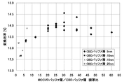
図4にMOCVDバッファ層142/CBDバッファ層141の膜厚比と、変換効率(%)の関係を示し、図5にMOCVDバッファ層142/CBDバッファ層141の膜厚比と、曲線因子(FF)との関係を示す。
また、図6にMOCVDバッファ層143の膜厚と太陽電池の変換効率の特性のグラフを示し、図7にMOCVDバッファ層143の膜厚(nm)と、太陽電池の曲線因子(FF)の関係をそれぞれ示す。
図4のグラフでは、横軸にMOCVDバッファ層142/Cホウ素(B)Dバッファ層141の膜厚比、縦軸に変換効率(%)、図5のグラフでは、横軸にMOCVDバッファ層142/CBDバッファ層141の膜厚比、縦軸に変換効率(%)を示している。
そして、それぞれのグラフにおいて、CBDバッファ層141の膜厚に応じた変換効率、曲線因子(FF)の変化を表している。また、図2〜図5においては、MOCVDバッファ層143の膜厚は70nm、抵抗率は0.5Ωcmである。
そして、それぞれのグラフにおいて、MOCVDバッファ層143の抵抗率に応じた変換効率、曲線因子(FF)の変化を表している。
まず、ガラス基板11上に金属裏面電極層12の電極パターンP1を形成し、その上に光吸収層13及びCBDバッファ層141、MOCVDバッファ層142を製膜する。
そして、MOCVDバッファ層142を製膜した時点で、メカニカルスクライブ装置又はレーザスクライブ装置により光吸収層13及びCBDバッファ層141、MOCVDバッファ層142を削ることによりパターン2を形成し、その上にさらに有機金属化学的気相成長法(MOCVD法)により第3のバッファ層としてMOCVDバッファ層143を製膜したものである。
また、MOCVDバッファ層143は、配線パターンの端面という製膜しにくい部分であるが、有機金属化学的気相成長法(MOCVD法)により製膜することで、カバーレッジよく製膜することができる。
12 金属裏面電極層
13 光吸収層
14 高抵抗バッファ層
15 窓層
141 CBDバッファ層(第1のバッファ層)
142 MOCVDバッファ層(第2のバッファ層)
143 MOCVDバッファ層(第3のバッファ層)
P1 パターン1
P2 パターン2
P3 パターン3
Claims (15)
- p型CIS系光吸収層、バッファ層、n型透明導電膜の順に積層されたCIS系薄膜太陽電池において、
前記バッファ層は3層以上の積層構造であり、
前記p型CIS系光吸収層と接する第1のバッファ層は、カドミウム(Cd)、又は、亜鉛(Zn)、又は、インジウム(In)を含む化合物からなり、
前記第1のバッファ層と接する第2のバッファ層は酸化亜鉛系薄膜からなり、
前記p型CIS系光吸収層、前記第1のバッファ層及び第2のバッファ層に配線パターンを形成することにより露出した端面及び、前記第2のバッファ層の前記n型透明導電膜との間の端面を覆う第3のバッファ層が形成されており、
前記第3のバッファ層は、酸化亜鉛系薄膜からなり、抵抗率が0.1〜100Ωcmの範囲内である、
ことを特徴とするCIS系薄膜太陽電池の集積構造。 - 前記第3のバッファ層の抵抗率が、前記第2のバッファ層の抵抗率より小さい、
請求項1記載のCIS系薄膜太陽電池の集積構造。 - 前記第3のバッファ層の膜厚が10〜300nmの範囲内である、
請求項1又は2記載のCIS系薄膜太陽電池の集積構造。 - 前記第3のバッファ層が有機金属化学的気相成長法(MOCVD法)により形成される、
請求項1〜3のいずれかに記載のCIS系薄膜太陽電池の集積構造。 - 前記第3のバッファ層に含まれるドーピング不純物元素濃度が1×10¹⁹atoms/cm3以下である、
請求項1〜4のいずれかに記載のCIS系薄膜太陽電池の集積構造。 - 前記ドーピング不純物元素が、アルミニウム(Al)、ガリウム(Ga)、ホウ素(B)のいずれかである、
請求項5記載のCIS系薄膜太陽電池の集積構造。 - 前記第1のバッファ層の膜厚が20nm以下、かつ、前記第2のバッファ層の膜厚が100nm以上である、
請求項1〜6のいずれかに記載のCIS系薄膜太陽電池の集積構造。 - 前記第1のバッファ層の膜厚と、前記第2のバッファ層の膜厚の比(第2のバッファ層の膜厚/第1のバッファ層の膜厚)が5以上である、
請求項1〜7のいずれかに記載のCIS系薄膜太陽電池の集積構造。 - 前記第1のバッファ層が、溶液成長法(CBD法)により形成される、
請求項1〜8のいずれかに記載のCIS系薄膜太陽電池の集積構造。 - 前記第2のバッファ層が、有機金属化学的気相成長法(MOCVD法)により形成される、
請求項1〜9のいずれかに記載のCIS系薄膜太陽電池の集積構造。 - 前記第2のバッファ層に含まれるドーピング不純物元素濃度が、1×10¹⁹atoms/cm3以下である、
請求項1〜10のいずれかに記載のCIS系薄膜太陽電池の集積構造。 - 前記ドーピング不純物元素が、アルミニウム(Al)、ガリウム(Ga)、ホウ素(B)のいずれかである、
請求項11記載のCIS系薄膜太陽電池の集積構造。 - 前記第1のバッファ層が、CdxSy、ZnxSy、ZnxOy、Znx(OH)y、InxSy、Inx(OH)y、InxOy(x、yは自然数)のいずれかを含む化合物である、
請求項1〜12のいずれかに記載のCIS系薄膜太陽電池の集積構造。 - 前記CIS系光吸収層表面における硫黄濃度が、0.5atoms%以上である、
請求項1〜13のいずれかに記載のCIS系薄膜太陽電池の集積構造。 - 前記第2のバッファ層の抵抗率が0.1Ωcm以上である、
請求項1〜14のいずれかに記載のCIS系薄膜太陽電池の集積構造。
Applications Claiming Priority (1)
| Application Number | Priority Date | Filing Date | Title |
|---|---|---|---|
| PCT/JP2008/054157 WO2009110093A1 (ja) | 2008-03-07 | 2008-03-07 | Cis系太陽電池の集積構造 |
Publications (2)
| Publication Number | Publication Date |
|---|---|
| JPWO2009110093A1 JPWO2009110093A1 (ja) | 2011-07-14 |
| JP5156090B2 true JP5156090B2 (ja) | 2013-03-06 |
Family
ID=41055672
Family Applications (1)
| Application Number | Title | Priority Date | Filing Date |
|---|---|---|---|
| JP2010501745A Expired - Fee Related JP5156090B2 (ja) | 2008-03-07 | 2008-03-07 | Cis系太陽電池の集積構造 |
Country Status (6)
| Country | Link |
|---|---|
| US (1) | US8575478B2 (ja) |
| JP (1) | JP5156090B2 (ja) |
| KR (1) | KR101488413B1 (ja) |
| DE (1) | DE112008003755T5 (ja) |
| TW (1) | TW200939499A (ja) |
| WO (1) | WO2009110093A1 (ja) |
Families Citing this family (23)
| Publication number | Priority date | Publication date | Assignee | Title |
|---|---|---|---|---|
| KR101034150B1 (ko) | 2009-11-02 | 2011-05-13 | 엘지이노텍 주식회사 | 태양전지 및 이의 제조방법 |
| KR101210168B1 (ko) * | 2010-03-24 | 2012-12-07 | 엘지이노텍 주식회사 | 태양광 발전장치 및 이의 제조방법 |
| KR101091361B1 (ko) * | 2010-07-30 | 2011-12-07 | 엘지이노텍 주식회사 | 태양광 발전장치 및 이의 제조방법 |
| US20120204939A1 (en) * | 2010-08-23 | 2012-08-16 | Stion Corporation | Structure and Method for High Efficiency CIS/CIGS-based Tandem Photovoltaic Module |
| CN103283031B (zh) * | 2010-09-22 | 2016-08-17 | 第一太阳能有限公司 | 包含n型掺杂剂源的光伏装置 |
| JP5500059B2 (ja) * | 2010-12-07 | 2014-05-21 | 株式会社豊田中央研究所 | 光電素子 |
| JPWO2012086703A1 (ja) * | 2010-12-22 | 2014-05-22 | 京セラ株式会社 | 光電変換装置 |
| KR101154786B1 (ko) * | 2011-05-31 | 2012-06-18 | 중앙대학교 산학협력단 | 태양전지 및 이의 제조방법 |
| KR101262573B1 (ko) * | 2011-07-29 | 2013-05-08 | 엘지이노텍 주식회사 | 태양전지 및 그의 제조방법 |
| KR101273093B1 (ko) * | 2011-07-29 | 2013-06-13 | 엘지이노텍 주식회사 | 태양전지 및 이의 제조방법 |
| KR101327126B1 (ko) * | 2011-10-05 | 2013-11-07 | 엘지이노텍 주식회사 | 태양전지 및 이를 이용한 태양전지 모듈 |
| KR101210046B1 (ko) | 2011-10-17 | 2012-12-07 | 엘지이노텍 주식회사 | 태양전지 및 이의 제조방법 |
| KR20130136739A (ko) * | 2012-06-05 | 2013-12-13 | 엘지이노텍 주식회사 | 태양전지 및 이의 제조방법 |
| US8697478B2 (en) * | 2012-09-06 | 2014-04-15 | Tsmc Solar Ltd. | Cover for protecting solar cells during fabrication |
| KR101923729B1 (ko) * | 2012-10-29 | 2018-11-29 | 한국전자통신연구원 | 태양전지의 제조방법 |
| WO2014077395A1 (ja) * | 2012-11-19 | 2014-05-22 | 東ソー株式会社 | 酸化物焼結体、それを用いたスパッタリングターゲット及び酸化物膜 |
| KR101415251B1 (ko) * | 2013-03-12 | 2014-07-07 | 한국에너지기술연구원 | 다중 버퍼층 및 이를 포함하는 태양전지 및 그 생산방법 |
| US9240501B2 (en) * | 2014-02-12 | 2016-01-19 | Solar Frontier K.K. | Compound-based thin film solar cell |
| US20180308995A1 (en) * | 2015-10-19 | 2018-10-25 | Solar Frontier K.K. | Photoelectric conversion element |
| CN105514215A (zh) * | 2015-12-16 | 2016-04-20 | 山东建筑大学 | 一种用氧化锌制备硫化锌光电薄膜的方法 |
| US10478518B2 (en) * | 2016-03-02 | 2019-11-19 | Better Vision Solutions LLC | Method for disinfecting contact lenses |
| WO2017200612A1 (en) | 2016-05-18 | 2017-11-23 | Menzel Diversified Enterprises, LLC | Insulated container |
| US10583977B2 (en) * | 2016-08-16 | 2020-03-10 | Mp Global Products, L.L.C. | Method of making an insulation material and an insulated mailer |
Citations (14)
| Publication number | Priority date | Publication date | Assignee | Title |
|---|---|---|---|---|
| JPH0494174A (ja) * | 1990-08-10 | 1992-03-26 | Fuji Electric Co Ltd | 化合物薄膜太陽電池およびその製造方法 |
| JPH10144946A (ja) * | 1996-11-08 | 1998-05-29 | Showa Shell Sekiyu Kk | 薄膜太陽電池の透明導電膜及び該透明導電膜の製造 方法 |
| JPH11220151A (ja) * | 1998-02-02 | 1999-08-10 | Shinko Electric Ind Co Ltd | 化合物半導体薄膜光電変換素子 |
| JP2000323733A (ja) * | 1999-03-05 | 2000-11-24 | Matsushita Electric Ind Co Ltd | 太陽電池 |
| JP2000332273A (ja) * | 1999-05-25 | 2000-11-30 | Matsushita Electric Ind Co Ltd | 太陽電池およびその製造方法 |
| JP2002124688A (ja) * | 2000-10-18 | 2002-04-26 | Matsushita Electric Ind Co Ltd | 太陽電池 |
| JP2002319686A (ja) * | 2001-04-23 | 2002-10-31 | Matsushita Electric Ind Co Ltd | 集積型薄膜太陽電池の製造方法 |
| JP2002373995A (ja) * | 2001-06-15 | 2002-12-26 | Honda Motor Co Ltd | 太陽電池の製造方法 |
| JP2004103959A (ja) * | 2002-09-11 | 2004-04-02 | Matsushita Electric Ind Co Ltd | 太陽電池およびその製造方法 |
| JP2004119953A (ja) * | 2002-09-26 | 2004-04-15 | Honda Motor Co Ltd | 薄膜太陽電池およびその製造方法 |
| JP2004214300A (ja) * | 2002-12-27 | 2004-07-29 | National Institute Of Advanced Industrial & Technology | ヘテロ接合を有する太陽電池 |
| JP2005191167A (ja) * | 2003-12-25 | 2005-07-14 | Showa Shell Sekiyu Kk | 集積型薄膜太陽電池及びその製造方法 |
| JP2006332190A (ja) * | 2005-05-24 | 2006-12-07 | Honda Motor Co Ltd | カルコパイライト型太陽電池 |
| JP2007287926A (ja) * | 2006-04-17 | 2007-11-01 | Kaneka Corp | 集積化薄膜光電変換装置の製造方法および、その製造方法で得られうる集積化薄膜光電変換装置。 |
Family Cites Families (9)
| Publication number | Priority date | Publication date | Assignee | Title |
|---|---|---|---|---|
| US4335266A (en) * | 1980-12-31 | 1982-06-15 | The Boeing Company | Methods for forming thin-film heterojunction solar cells from I-III-VI.sub.2 |
| US4611091A (en) | 1984-12-06 | 1986-09-09 | Atlantic Richfield Company | CuInSe2 thin film solar cell with thin CdS and transparent window layer |
| JPH03249342A (ja) | 1990-02-28 | 1991-11-07 | Mitsubishi Motors Corp | 混合燃料エンジン用燃料供給装置 |
| JPH0766984B2 (ja) * | 1992-02-13 | 1995-07-19 | インターナショナル・ビジネス・マシーンズ・コーポレイション | ヘテロ超格子pn接合 |
| JP3402515B2 (ja) * | 1994-05-23 | 2003-05-06 | 日本碍子株式会社 | 水素分離体とそれを用いた水素分離装置及び水素分離体の製造方法 |
| US6259016B1 (en) | 1999-03-05 | 2001-07-10 | Matsushita Electric Industrial Co., Ltd. | Solar cell |
| JP2002094089A (ja) * | 2000-09-11 | 2002-03-29 | Honda Motor Co Ltd | 化合物薄膜太陽電池の製造方法 |
| SE0301350D0 (sv) * | 2003-05-08 | 2003-05-08 | Forskarpatent I Uppsala Ab | A thin-film solar cell |
| JP4841173B2 (ja) | 2005-05-27 | 2011-12-21 | 昭和シェル石油株式会社 | Cis系薄膜太陽電池の高抵抗バッファ層・窓層連続製膜方法及び製膜装置 |
-
2008
- 2008-03-07 DE DE112008003755T patent/DE112008003755T5/de not_active Withdrawn
- 2008-03-07 JP JP2010501745A patent/JP5156090B2/ja not_active Expired - Fee Related
- 2008-03-07 US US12/921,222 patent/US8575478B2/en not_active Expired - Fee Related
- 2008-03-07 KR KR1020107019676A patent/KR101488413B1/ko active IP Right Grant
- 2008-03-07 WO PCT/JP2008/054157 patent/WO2009110093A1/ja active Application Filing
- 2008-05-07 TW TW097116848A patent/TW200939499A/zh unknown
Patent Citations (14)
| Publication number | Priority date | Publication date | Assignee | Title |
|---|---|---|---|---|
| JPH0494174A (ja) * | 1990-08-10 | 1992-03-26 | Fuji Electric Co Ltd | 化合物薄膜太陽電池およびその製造方法 |
| JPH10144946A (ja) * | 1996-11-08 | 1998-05-29 | Showa Shell Sekiyu Kk | 薄膜太陽電池の透明導電膜及び該透明導電膜の製造 方法 |
| JPH11220151A (ja) * | 1998-02-02 | 1999-08-10 | Shinko Electric Ind Co Ltd | 化合物半導体薄膜光電変換素子 |
| JP2000323733A (ja) * | 1999-03-05 | 2000-11-24 | Matsushita Electric Ind Co Ltd | 太陽電池 |
| JP2000332273A (ja) * | 1999-05-25 | 2000-11-30 | Matsushita Electric Ind Co Ltd | 太陽電池およびその製造方法 |
| JP2002124688A (ja) * | 2000-10-18 | 2002-04-26 | Matsushita Electric Ind Co Ltd | 太陽電池 |
| JP2002319686A (ja) * | 2001-04-23 | 2002-10-31 | Matsushita Electric Ind Co Ltd | 集積型薄膜太陽電池の製造方法 |
| JP2002373995A (ja) * | 2001-06-15 | 2002-12-26 | Honda Motor Co Ltd | 太陽電池の製造方法 |
| JP2004103959A (ja) * | 2002-09-11 | 2004-04-02 | Matsushita Electric Ind Co Ltd | 太陽電池およびその製造方法 |
| JP2004119953A (ja) * | 2002-09-26 | 2004-04-15 | Honda Motor Co Ltd | 薄膜太陽電池およびその製造方法 |
| JP2004214300A (ja) * | 2002-12-27 | 2004-07-29 | National Institute Of Advanced Industrial & Technology | ヘテロ接合を有する太陽電池 |
| JP2005191167A (ja) * | 2003-12-25 | 2005-07-14 | Showa Shell Sekiyu Kk | 集積型薄膜太陽電池及びその製造方法 |
| JP2006332190A (ja) * | 2005-05-24 | 2006-12-07 | Honda Motor Co Ltd | カルコパイライト型太陽電池 |
| JP2007287926A (ja) * | 2006-04-17 | 2007-11-01 | Kaneka Corp | 集積化薄膜光電変換装置の製造方法および、その製造方法で得られうる集積化薄膜光電変換装置。 |
Also Published As
| Publication number | Publication date |
|---|---|
| US20110011451A1 (en) | 2011-01-20 |
| US8575478B2 (en) | 2013-11-05 |
| JPWO2009110093A1 (ja) | 2011-07-14 |
| KR101488413B1 (ko) | 2015-01-30 |
| KR20100124741A (ko) | 2010-11-29 |
| DE112008003755T5 (de) | 2011-02-24 |
| TW200939499A (en) | 2009-09-16 |
| WO2009110093A1 (ja) | 2009-09-11 |
Similar Documents
| Publication | Publication Date | Title |
|---|---|---|
| JP5156090B2 (ja) | Cis系太陽電池の集積構造 | |
| WO2009110092A1 (ja) | Cis系太陽電池の積層構造、及び集積構造 | |
| US9935211B2 (en) | Back contact structure for photovoltaic devices such as copper-indium-diselenide solar cells | |
| WO2011158899A1 (ja) | Cis系薄膜太陽電池 | |
| WO2013077417A1 (ja) | Czts系薄膜太陽電池及びその製造方法 | |
| JP6377338B2 (ja) | 光電変換素子、光電変換素子の製造方法及び太陽電池 | |
| JP2016063160A (ja) | 光電変換素子および太陽電池 | |
| JP2014209586A (ja) | 薄膜太陽電池及びその製造方法 | |
| Nakada et al. | Improved efficiency of Cu (In, Ga) Se/sub 2/thin film solar cells with chemically deposited ZnS buffer layers by air-annealing-formation of homojunction by solid phase diffusion | |
| JP2014503125A (ja) | 太陽電池及びその製造方法 | |
| JP5421752B2 (ja) | 化合物半導体太陽電池 | |
| JP2009170928A (ja) | Cis系太陽電池の製造方法 | |
| JP5245034B2 (ja) | Cis系太陽電池の製造方法 | |
| JP2017059656A (ja) | 光電変換素子および太陽電池 | |
| Breeze | Next generation thin-film solar cells | |
| KR20090034079A (ko) | 이셀렌화몰리브덴층을 포함하는 태양전지 및 그의 제조방법 | |
| US20150093852A1 (en) | Method for enhancing conductivity of molybdenum thin film by using electron beam irradiation | |
| KR101283240B1 (ko) | 태양전지 및 이의 제조방법 | |
| JP5420775B2 (ja) | Cis系太陽電池の製造方法 | |
| JP5918765B2 (ja) | 太陽光発電装置 | |
| KR20110116485A (ko) | 태양 전지 제조 방법 | |
| KR101300642B1 (ko) | 태양전지 | |
| JP2013229506A (ja) | 太陽電池 | |
| WO2017068923A1 (ja) | 光電変換素子 | |
| JP2011091249A (ja) | 太陽電池 |
Legal Events
| Date | Code | Title | Description |
|---|---|---|---|
| A621 | Written request for application examination |
Free format text: JAPANESE INTERMEDIATE CODE: A621 Effective date: 20110304 |
|
| A521 | Request for written amendment filed |
Free format text: JAPANESE INTERMEDIATE CODE: A523 Effective date: 20120604 |
|
| A131 | Notification of reasons for refusal |
Free format text: JAPANESE INTERMEDIATE CODE: A131 Effective date: 20120809 |
|
| A521 | Request for written amendment filed |
Free format text: JAPANESE INTERMEDIATE CODE: A523 Effective date: 20121005 |
|
| TRDD | Decision of grant or rejection written | ||
| A01 | Written decision to grant a patent or to grant a registration (utility model) |
Free format text: JAPANESE INTERMEDIATE CODE: A01 Effective date: 20121204 |
|
| A61 | First payment of annual fees (during grant procedure) |
Free format text: JAPANESE INTERMEDIATE CODE: A61 Effective date: 20121207 |
|
| FPAY | Renewal fee payment (event date is renewal date of database) |
Free format text: PAYMENT UNTIL: 20151214 Year of fee payment: 3 |
|
| R150 | Certificate of patent or registration of utility model |
Ref document number: 5156090 Country of ref document: JP Free format text: JAPANESE INTERMEDIATE CODE: R150 Free format text: JAPANESE INTERMEDIATE CODE: R150 |
|
| S111 | Request for change of ownership or part of ownership |
Free format text: JAPANESE INTERMEDIATE CODE: R313111 |
|
| R350 | Written notification of registration of transfer |
Free format text: JAPANESE INTERMEDIATE CODE: R350 |
|
| R250 | Receipt of annual fees |
Free format text: JAPANESE INTERMEDIATE CODE: R250 |
|
| R250 | Receipt of annual fees |
Free format text: JAPANESE INTERMEDIATE CODE: R250 |
|
| R250 | Receipt of annual fees |
Free format text: JAPANESE INTERMEDIATE CODE: R250 |
|
| R250 | Receipt of annual fees |
Free format text: JAPANESE INTERMEDIATE CODE: R250 |
|
| R250 | Receipt of annual fees |
Free format text: JAPANESE INTERMEDIATE CODE: R250 |
|
| R250 | Receipt of annual fees |
Free format text: JAPANESE INTERMEDIATE CODE: R250 |
|
| LAPS | Cancellation because of no payment of annual fees |