JP5132404B2 - 半導体発光装置 - Google Patents
半導体発光装置 Download PDFInfo
- Publication number
- JP5132404B2 JP5132404B2 JP2008108059A JP2008108059A JP5132404B2 JP 5132404 B2 JP5132404 B2 JP 5132404B2 JP 2008108059 A JP2008108059 A JP 2008108059A JP 2008108059 A JP2008108059 A JP 2008108059A JP 5132404 B2 JP5132404 B2 JP 5132404B2
- Authority
- JP
- Japan
- Prior art keywords
- light emitting
- wiring pattern
- semiconductor light
- emitting element
- substrate
- Prior art date
- Legal status (The legal status is an assumption and is not a legal conclusion. Google has not performed a legal analysis and makes no representation as to the accuracy of the status listed.)
- Expired - Fee Related
Links
Images


Classifications
-
- H—ELECTRICITY
- H01—ELECTRIC ELEMENTS
- H01L—SEMICONDUCTOR DEVICES NOT COVERED BY CLASS H10
- H01L25/00—Assemblies consisting of a plurality of individual semiconductor or other solid state devices ; Multistep manufacturing processes thereof
- H01L25/03—Assemblies consisting of a plurality of individual semiconductor or other solid state devices ; Multistep manufacturing processes thereof all the devices being of a type provided for in the same subgroup of groups H01L27/00 - H01L33/00, or in a single subclass of H10K, H10N, e.g. assemblies of rectifier diodes
- H01L25/04—Assemblies consisting of a plurality of individual semiconductor or other solid state devices ; Multistep manufacturing processes thereof all the devices being of a type provided for in the same subgroup of groups H01L27/00 - H01L33/00, or in a single subclass of H10K, H10N, e.g. assemblies of rectifier diodes the devices not having separate containers
- H01L25/075—Assemblies consisting of a plurality of individual semiconductor or other solid state devices ; Multistep manufacturing processes thereof all the devices being of a type provided for in the same subgroup of groups H01L27/00 - H01L33/00, or in a single subclass of H10K, H10N, e.g. assemblies of rectifier diodes the devices not having separate containers the devices being of a type provided for in group H01L33/00
- H01L25/0753—Assemblies consisting of a plurality of individual semiconductor or other solid state devices ; Multistep manufacturing processes thereof all the devices being of a type provided for in the same subgroup of groups H01L27/00 - H01L33/00, or in a single subclass of H10K, H10N, e.g. assemblies of rectifier diodes the devices not having separate containers the devices being of a type provided for in group H01L33/00 the devices being arranged next to each other
-
- H—ELECTRICITY
- H01—ELECTRIC ELEMENTS
- H01L—SEMICONDUCTOR DEVICES NOT COVERED BY CLASS H10
- H01L2224/00—Indexing scheme for arrangements for connecting or disconnecting semiconductor or solid-state bodies and methods related thereto as covered by H01L24/00
- H01L2224/01—Means for bonding being attached to, or being formed on, the surface to be connected, e.g. chip-to-package, die-attach, "first-level" interconnects; Manufacturing methods related thereto
- H01L2224/42—Wire connectors; Manufacturing methods related thereto
- H01L2224/44—Structure, shape, material or disposition of the wire connectors prior to the connecting process
- H01L2224/45—Structure, shape, material or disposition of the wire connectors prior to the connecting process of an individual wire connector
- H01L2224/45001—Core members of the connector
- H01L2224/45099—Material
- H01L2224/451—Material with a principal constituent of the material being a metal or a metalloid, e.g. boron (B), silicon (Si), germanium (Ge), arsenic (As), antimony (Sb), tellurium (Te) and polonium (Po), and alloys thereof
- H01L2224/45138—Material with a principal constituent of the material being a metal or a metalloid, e.g. boron (B), silicon (Si), germanium (Ge), arsenic (As), antimony (Sb), tellurium (Te) and polonium (Po), and alloys thereof the principal constituent melting at a temperature of greater than or equal to 950°C and less than 1550°C
- H01L2224/45144—Gold (Au) as principal constituent
-
- H—ELECTRICITY
- H01—ELECTRIC ELEMENTS
- H01L—SEMICONDUCTOR DEVICES NOT COVERED BY CLASS H10
- H01L2224/00—Indexing scheme for arrangements for connecting or disconnecting semiconductor or solid-state bodies and methods related thereto as covered by H01L24/00
- H01L2224/01—Means for bonding being attached to, or being formed on, the surface to be connected, e.g. chip-to-package, die-attach, "first-level" interconnects; Manufacturing methods related thereto
- H01L2224/42—Wire connectors; Manufacturing methods related thereto
- H01L2224/47—Structure, shape, material or disposition of the wire connectors after the connecting process
- H01L2224/48—Structure, shape, material or disposition of the wire connectors after the connecting process of an individual wire connector
- H01L2224/4805—Shape
- H01L2224/4809—Loop shape
- H01L2224/48091—Arched
-
- H—ELECTRICITY
- H01—ELECTRIC ELEMENTS
- H01L—SEMICONDUCTOR DEVICES NOT COVERED BY CLASS H10
- H01L2224/00—Indexing scheme for arrangements for connecting or disconnecting semiconductor or solid-state bodies and methods related thereto as covered by H01L24/00
- H01L2224/01—Means for bonding being attached to, or being formed on, the surface to be connected, e.g. chip-to-package, die-attach, "first-level" interconnects; Manufacturing methods related thereto
- H01L2224/42—Wire connectors; Manufacturing methods related thereto
- H01L2224/47—Structure, shape, material or disposition of the wire connectors after the connecting process
- H01L2224/48—Structure, shape, material or disposition of the wire connectors after the connecting process of an individual wire connector
- H01L2224/481—Disposition
- H01L2224/48135—Connecting between different semiconductor or solid-state bodies, i.e. chip-to-chip
- H01L2224/48137—Connecting between different semiconductor or solid-state bodies, i.e. chip-to-chip the bodies being arranged next to each other, e.g. on a common substrate
-
- H—ELECTRICITY
- H01—ELECTRIC ELEMENTS
- H01L—SEMICONDUCTOR DEVICES NOT COVERED BY CLASS H10
- H01L2224/00—Indexing scheme for arrangements for connecting or disconnecting semiconductor or solid-state bodies and methods related thereto as covered by H01L24/00
- H01L2224/01—Means for bonding being attached to, or being formed on, the surface to be connected, e.g. chip-to-package, die-attach, "first-level" interconnects; Manufacturing methods related thereto
- H01L2224/42—Wire connectors; Manufacturing methods related thereto
- H01L2224/47—Structure, shape, material or disposition of the wire connectors after the connecting process
- H01L2224/48—Structure, shape, material or disposition of the wire connectors after the connecting process of an individual wire connector
- H01L2224/481—Disposition
- H01L2224/48151—Connecting between a semiconductor or solid-state body and an item not being a semiconductor or solid-state body, e.g. chip-to-substrate, chip-to-passive
- H01L2224/48221—Connecting between a semiconductor or solid-state body and an item not being a semiconductor or solid-state body, e.g. chip-to-substrate, chip-to-passive the body and the item being stacked
- H01L2224/48225—Connecting between a semiconductor or solid-state body and an item not being a semiconductor or solid-state body, e.g. chip-to-substrate, chip-to-passive the body and the item being stacked the item being non-metallic, e.g. insulating substrate with or without metallisation
- H01L2224/48227—Connecting between a semiconductor or solid-state body and an item not being a semiconductor or solid-state body, e.g. chip-to-substrate, chip-to-passive the body and the item being stacked the item being non-metallic, e.g. insulating substrate with or without metallisation connecting the wire to a bond pad of the item
-
- H—ELECTRICITY
- H01—ELECTRIC ELEMENTS
- H01L—SEMICONDUCTOR DEVICES NOT COVERED BY CLASS H10
- H01L33/00—Semiconductor devices with at least one potential-jump barrier or surface barrier specially adapted for light emission; Processes or apparatus specially adapted for the manufacture or treatment thereof or of parts thereof; Details thereof
- H01L33/48—Semiconductor devices with at least one potential-jump barrier or surface barrier specially adapted for light emission; Processes or apparatus specially adapted for the manufacture or treatment thereof or of parts thereof; Details thereof characterised by the semiconductor body packages
- H01L33/483—Containers
- H01L33/486—Containers adapted for surface mounting
-
- H—ELECTRICITY
- H01—ELECTRIC ELEMENTS
- H01L—SEMICONDUCTOR DEVICES NOT COVERED BY CLASS H10
- H01L33/00—Semiconductor devices with at least one potential-jump barrier or surface barrier specially adapted for light emission; Processes or apparatus specially adapted for the manufacture or treatment thereof or of parts thereof; Details thereof
- H01L33/48—Semiconductor devices with at least one potential-jump barrier or surface barrier specially adapted for light emission; Processes or apparatus specially adapted for the manufacture or treatment thereof or of parts thereof; Details thereof characterised by the semiconductor body packages
- H01L33/62—Arrangements for conducting electric current to or from the semiconductor body, e.g. lead-frames, wire-bonds or solder balls
Description
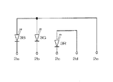
第一の半導体発光素子は、第二の半導体発光素子より静電耐圧が高く、第一の配線パターンおよび第二の配線パターンは電気的に独立して形成され、第一の配線パターンおよび第二の配線パターンの封止樹脂部から露出した部分において、第一の配線パターンは、第二の配線パターンより実装面から離れる方向に遠い位置に配置されていることを特徴とする。
2:配線パターン
3:半導体発光素子
4:導電ワイヤ
5:封止樹脂部
6:スルーホール
7:回路パターン
8:レジスト層
Claims (4)
- 第一の半導体発光素子および第二の半導体発光素子が上面に搭載され、前記上面と隣接する一側面を実装面とする基板と、
前記第一の半導体発光素子および前記第二の半導体発光素子にそれぞれ電気的に接続された第一の配線パターンおよび第二の配線パターンと、
前記基板上において、前記第一の配線パターンおよび前記第二の配線パターンの一部、前記第一の半導体発光素子および前記第二の半導体発光素子を覆う封止樹脂部と、を有し、
前記第一の半導体発光素子は、前記第二の半導体発光素子より静電耐圧が高く、
前記第一の配線パターンおよび前記第二の配線パターンは電気的に独立して形成され、
前記第一の配線パターンおよび前記第二の配線パターンの前記封止樹脂部から露出した部分において、前記第一の配線パターンに接続された誘導端子を有し、
前記誘導端子は、前記第二の配線パターンより前記実装面から離れる方向に遠い位置に配置されていることを特徴とする半導体発光装置。 - 第一の半導体発光素子および第二の半導体発光素子が上面に搭載され、前記上面と隣接する一側面を実装面とする基板と、
前記第一の半導体発光素子および前記第二の半導体発光素子にそれぞれ電気的に接続され、それぞれ正・負の電極パターンからなる第一の配線パターンおよび第二の配線パターンと、
前記基板上において、前記第一の配線パターンおよび前記第二の配線パターンの一部、前記第一の半導体発光素子および前記第二の半導体発光素子を覆う封止樹脂部と、を有し、
前記第一の半導体発光素子は、前記第二の半導体発光素子より静電耐圧が高く、
前記第一の配線パターンおよび前記第二の配線パターンは、正・負いずれかの電極パターンが電気的に共通し、他方の電極パターンが電気的に独立するよう形成され、
前記第一の配線パターンおよび前記第二の配線パターンの前記封止樹脂部から露出した部分において、前記第一の配線パターンの前記第二の配線パターンと電気的に独立して形成された電極パターンは前記第一の配線パターンに接続された誘導端子を有し、
前記誘導端子は、前記第二の配線パターンより前記実装面から離れる方向に遠い位置に配置されていることを特徴とする半導体発光装置。 - 第一の半導体発光素子および第二の半導体発光素子が上面に搭載され、前記上面と隣接する一側面を実装面とする基板と、
前記第一の半導体発光素子および前記第二の半導体発光素子にそれぞれ電気的に接続された第一の配線パターンおよび第二の配線パターンと、
前記基板上において、前記第一の配線パターンおよび前記第二の配線パターンの一部、前記第一の半導体発光素子および前記第二の半導体発光素子を覆う封止樹脂部と、
前記基板上において、前記配線パターンの一部を覆う絶縁膜と、を有し、
前記第一の半導体発光素子は、前記第二の半導体発光素子より静電耐圧が高く、
前記第一の配線パターンおよび前記第二の配線パターンは電気的に独立して形成され、
前記第一の配線パターンおよび前記第二の配線パターンの前記封止樹脂部および前記絶縁膜から露出した部分において、前記第一の配線パターンに接続された誘導端子を有し、
前記誘導端子は、前記第二の配線パターンより前記実装面から離れる方向に遠い位置に配置されていることを特徴とする半導体発光装置。 - 第一の半導体発光素子および第二の半導体発光素子が上面に搭載され、前記上面と隣接する一側面を実装面とする基板と、
前記第一の半導体発光素子および前記第二の半導体発光素子にそれぞれ電気的に接続され、それぞれ正・負の電極パターンからなる第一の配線パターンおよび第二の配線パターンと、
前記基板上において、前記第一の配線パターンおよび前記第二の配線パターンの一部、前記第一の半導体発光素子および前記第二の半導体発光素子を覆う封止樹脂部と、
前記基板上において、前記配線パターンの一部を覆う絶縁膜と、を有し、
前記第一の半導体発光素子は、前記第二の半導体発光素子より静電耐圧が高く、
前記第一の配線パターンおよび前記第二の配線パターンは、正・負いずれかの電極パターンが電気的に共通し、他方の電極パターンが電気的に独立するよう形成され、
前記第一の配線パターンおよび前記第二の配線パターンの前記封止樹脂部および前記絶縁膜から露出した部分において、前記第一の配線パターンの前記第二の配線パターンと電気的に独立して形成された電極パターンは前記第一の配線パターンに接続された誘導端子を有し、
前記誘導端子は、前記第二の配線パターンより前記実装面から離れる方向に遠い位置に配置されていることを特徴とする半導体発光装置。
Priority Applications (3)
| Application Number | Priority Date | Filing Date | Title |
|---|---|---|---|
| JP2008108059A JP5132404B2 (ja) | 2008-04-17 | 2008-04-17 | 半導体発光装置 |
| US12/424,423 US8106411B2 (en) | 2008-04-17 | 2009-04-15 | Light emitting device |
| CN2009101320491A CN101562178B (zh) | 2008-04-17 | 2009-04-15 | 半导体发光装置 |
Applications Claiming Priority (1)
| Application Number | Priority Date | Filing Date | Title |
|---|---|---|---|
| JP2008108059A JP5132404B2 (ja) | 2008-04-17 | 2008-04-17 | 半導体発光装置 |
Publications (3)
| Publication Number | Publication Date |
|---|---|
| JP2009260073A JP2009260073A (ja) | 2009-11-05 |
| JP2009260073A5 JP2009260073A5 (ja) | 2011-06-02 |
| JP5132404B2 true JP5132404B2 (ja) | 2013-01-30 |
Family
ID=41220900
Family Applications (1)
| Application Number | Title | Priority Date | Filing Date |
|---|---|---|---|
| JP2008108059A Expired - Fee Related JP5132404B2 (ja) | 2008-04-17 | 2008-04-17 | 半導体発光装置 |
Country Status (3)
| Country | Link |
|---|---|
| US (1) | US8106411B2 (ja) |
| JP (1) | JP5132404B2 (ja) |
| CN (1) | CN101562178B (ja) |
Families Citing this family (14)
| Publication number | Priority date | Publication date | Assignee | Title |
|---|---|---|---|---|
| JP2011146640A (ja) * | 2010-01-18 | 2011-07-28 | Fujikom Corp | Led光源 |
| KR101047778B1 (ko) | 2010-04-01 | 2011-07-07 | 엘지이노텍 주식회사 | 발광 소자 패키지 및 이를 구비한 라이트 유닛 |
| JP6131048B2 (ja) * | 2010-10-12 | 2017-05-17 | ローム株式会社 | Ledモジュール |
| JP5748496B2 (ja) | 2011-02-10 | 2015-07-15 | ローム株式会社 | Ledモジュール |
| JP2013026510A (ja) * | 2011-07-22 | 2013-02-04 | Rohm Co Ltd | Ledモジュールおよびledモジュールの実装構造 |
| WO2013127675A1 (en) * | 2012-02-28 | 2013-09-06 | Tp Vision Holding B.V. | Led with electro static discharge protection |
| US8876330B2 (en) * | 2012-11-15 | 2014-11-04 | Illinois Tool Works Inc. | Illumination device |
| TWM458672U (zh) * | 2013-04-10 | 2013-08-01 | Genesis Photonics Inc | 光源模組 |
| CN106299095A (zh) * | 2015-06-12 | 2017-01-04 | 映瑞光电科技(上海)有限公司 | 一种高压倒装led芯片及其制作方法 |
| JP2017143314A (ja) * | 2017-05-24 | 2017-08-17 | ローム株式会社 | Ledモジュール |
| JP6842485B2 (ja) * | 2019-03-04 | 2021-03-17 | ローム株式会社 | Ledモジュール |
| JP7231450B2 (ja) * | 2019-03-18 | 2023-03-01 | ローム株式会社 | 半導体発光装置 |
| JP7307874B2 (ja) | 2019-04-26 | 2023-07-13 | 日亜化学工業株式会社 | 発光装置及び発光モジュール |
| CN112242384A (zh) * | 2019-07-18 | 2021-01-19 | 高创(苏州)电子有限公司 | Led灯珠、led显示屏、led显示装置及驱动方法 |
Family Cites Families (11)
| Publication number | Priority date | Publication date | Assignee | Title |
|---|---|---|---|---|
| US6054716A (en) * | 1997-01-10 | 2000-04-25 | Rohm Co., Ltd. | Semiconductor light emitting device having a protecting device |
| JP3673621B2 (ja) | 1997-07-30 | 2005-07-20 | ローム株式会社 | チップ型発光素子 |
| JP2001196634A (ja) * | 2000-01-07 | 2001-07-19 | Nippon Sheet Glass Co Ltd | 発光ダイオードモジュール |
| JP2001196638A (ja) * | 2000-01-12 | 2001-07-19 | Toyoda Gosei Co Ltd | 発光ダイオードの静電保護装置 |
| JP2001345485A (ja) * | 2000-06-02 | 2001-12-14 | Toyoda Gosei Co Ltd | 発光装置 |
| JP2002344025A (ja) * | 2001-05-21 | 2002-11-29 | Stanley Electric Co Ltd | 多色式横方向発光型面実装led |
| JP4239509B2 (ja) * | 2002-08-02 | 2009-03-18 | 日亜化学工業株式会社 | 発光ダイオード |
| JP4598767B2 (ja) * | 2003-07-30 | 2010-12-15 | パナソニック株式会社 | 半導体発光装置、発光モジュール、および照明装置 |
| JP4902114B2 (ja) * | 2004-12-16 | 2012-03-21 | 日亜化学工業株式会社 | 発光装置 |
| JP4756682B2 (ja) * | 2005-05-16 | 2011-08-24 | シチズン電子株式会社 | 発光ダイオード光源ユニット及びバルブ型発光ダイオード光源 |
| US7479660B2 (en) * | 2005-10-21 | 2009-01-20 | Perkinelmer Elcos Gmbh | Multichip on-board LED illumination device |
-
2008
- 2008-04-17 JP JP2008108059A patent/JP5132404B2/ja not_active Expired - Fee Related
-
2009
- 2009-04-15 CN CN2009101320491A patent/CN101562178B/zh not_active Expired - Fee Related
- 2009-04-15 US US12/424,423 patent/US8106411B2/en not_active Expired - Fee Related
Also Published As
| Publication number | Publication date |
|---|---|
| US8106411B2 (en) | 2012-01-31 |
| CN101562178B (zh) | 2012-11-07 |
| US20090284130A1 (en) | 2009-11-19 |
| CN101562178A (zh) | 2009-10-21 |
| JP2009260073A (ja) | 2009-11-05 |
Similar Documents
| Publication | Publication Date | Title |
|---|---|---|
| JP5132404B2 (ja) | 半導体発光装置 | |
| EP2413392A2 (en) | Light-emitting diode package | |
| US9887338B2 (en) | Light emitting diode device | |
| EP2188849B1 (en) | Light emitting device | |
| JP6738785B2 (ja) | 発光デバイス及びその製造方法 | |
| JP6179583B2 (ja) | 電子装置 | |
| JP5041593B2 (ja) | チップ型半導体装置の製造方法 | |
| JP2015526908A (ja) | 発光ダイオード装置 | |
| JP2015005681A (ja) | 半導体装置及びその製造方法 | |
| JP2005057144A (ja) | 発光装置 | |
| JP2007088173A (ja) | 積層型チップバリスタ及び電子機器の製造方法 | |
| US7688591B2 (en) | Electronic-component-mounting board | |
| US20090154176A1 (en) | Electronic component and method for manufacturing same | |
| US20080225449A1 (en) | Electrostatic discharge protection component, and electronic component module using the same | |
| JP2008270327A (ja) | 静電気対策部品およびこれを用いた発光ダイオードモジュール | |
| JP2013219071A (ja) | 発光素子搭載用部品および発光装置 | |
| KR100674857B1 (ko) | 정전기 방전(esd)을 강화한 엘이디 패키지 및 그제조방법 | |
| KR20160126311A (ko) | 반도체 패키지 및 반도체 패키지의 제조방법 | |
| JP2005191097A (ja) | 半導体パッケージ | |
| JP2009188005A (ja) | 表面実装型半導体装置 | |
| JP2011077164A (ja) | 半導体発光装置 | |
| US9923123B2 (en) | Printed circuit board and light-emitting device including same | |
| KR20110073765A (ko) | 칩 저항기 및 이의 제조 방법 | |
| US10008651B2 (en) | Light emitting device and wiring board thereof | |
| JP2005277114A (ja) | 半導体装置 |
Legal Events
| Date | Code | Title | Description |
|---|---|---|---|
| A521 | Request for written amendment filed |
Free format text: JAPANESE INTERMEDIATE CODE: A523 Effective date: 20110414 |
|
| A621 | Written request for application examination |
Free format text: JAPANESE INTERMEDIATE CODE: A621 Effective date: 20110414 |
|
| A977 | Report on retrieval |
Free format text: JAPANESE INTERMEDIATE CODE: A971007 Effective date: 20120815 |
|
| A131 | Notification of reasons for refusal |
Free format text: JAPANESE INTERMEDIATE CODE: A131 Effective date: 20120828 |
|
| A521 | Request for written amendment filed |
Free format text: JAPANESE INTERMEDIATE CODE: A523 Effective date: 20120913 |
|
| TRDD | Decision of grant or rejection written | ||
| A01 | Written decision to grant a patent or to grant a registration (utility model) |
Free format text: JAPANESE INTERMEDIATE CODE: A01 Effective date: 20121009 |
|
| A01 | Written decision to grant a patent or to grant a registration (utility model) |
Free format text: JAPANESE INTERMEDIATE CODE: A01 |
|
| A61 | First payment of annual fees (during grant procedure) |
Free format text: JAPANESE INTERMEDIATE CODE: A61 Effective date: 20121106 |
|
| FPAY | Renewal fee payment (event date is renewal date of database) |
Free format text: PAYMENT UNTIL: 20151116 Year of fee payment: 3 |
|
| R150 | Certificate of patent or registration of utility model |
Free format text: JAPANESE INTERMEDIATE CODE: R150 Ref document number: 5132404 Country of ref document: JP Free format text: JAPANESE INTERMEDIATE CODE: R150 |
|
| R250 | Receipt of annual fees |
Free format text: JAPANESE INTERMEDIATE CODE: R250 |
|
| R250 | Receipt of annual fees |
Free format text: JAPANESE INTERMEDIATE CODE: R250 |
|
| R250 | Receipt of annual fees |
Free format text: JAPANESE INTERMEDIATE CODE: R250 |
|
| R250 | Receipt of annual fees |
Free format text: JAPANESE INTERMEDIATE CODE: R250 |
|
| R250 | Receipt of annual fees |
Free format text: JAPANESE INTERMEDIATE CODE: R250 |
|
| LAPS | Cancellation because of no payment of annual fees |