JP5004791B2 - Soiおよびバルク・シリコン領域を含む半導体デバイス内のsti形成 - Google Patents
Soiおよびバルク・シリコン領域を含む半導体デバイス内のsti形成 Download PDFInfo
- Publication number
- JP5004791B2 JP5004791B2 JP2007516538A JP2007516538A JP5004791B2 JP 5004791 B2 JP5004791 B2 JP 5004791B2 JP 2007516538 A JP2007516538 A JP 2007516538A JP 2007516538 A JP2007516538 A JP 2007516538A JP 5004791 B2 JP5004791 B2 JP 5004791B2
- Authority
- JP
- Japan
- Prior art keywords
- sti
- region
- silicon
- etching
- soi
- Prior art date
- Legal status (The legal status is an assumption and is not a legal conclusion. Google has not performed a legal analysis and makes no representation as to the accuracy of the status listed.)
- Expired - Fee Related
Links
Images


Classifications
-
- H—ELECTRICITY
- H01—ELECTRIC ELEMENTS
- H01L—SEMICONDUCTOR DEVICES NOT COVERED BY CLASS H10
- H01L21/00—Processes or apparatus adapted for the manufacture or treatment of semiconductor or solid state devices or of parts thereof
- H01L21/70—Manufacture or treatment of devices consisting of a plurality of solid state components formed in or on a common substrate or of parts thereof; Manufacture of integrated circuit devices or of parts thereof
- H01L21/71—Manufacture of specific parts of devices defined in group H01L21/70
- H01L21/76—Making of isolation regions between components
- H01L21/762—Dielectric regions, e.g. EPIC dielectric isolation, LOCOS; Trench refilling techniques, SOI technology, use of channel stoppers
- H01L21/7624—Dielectric regions, e.g. EPIC dielectric isolation, LOCOS; Trench refilling techniques, SOI technology, use of channel stoppers using semiconductor on insulator [SOI] technology
-
- H—ELECTRICITY
- H01—ELECTRIC ELEMENTS
- H01L—SEMICONDUCTOR DEVICES NOT COVERED BY CLASS H10
- H01L21/00—Processes or apparatus adapted for the manufacture or treatment of semiconductor or solid state devices or of parts thereof
- H01L21/02—Manufacture or treatment of semiconductor devices or of parts thereof
- H01L21/04—Manufacture or treatment of semiconductor devices or of parts thereof the devices having at least one potential-jump barrier or surface barrier, e.g. PN junction, depletion layer or carrier concentration layer
- H01L21/18—Manufacture or treatment of semiconductor devices or of parts thereof the devices having at least one potential-jump barrier or surface barrier, e.g. PN junction, depletion layer or carrier concentration layer the devices having semiconductor bodies comprising elements of Group IV of the Periodic System or AIIIBV compounds with or without impurities, e.g. doping materials
- H01L21/30—Treatment of semiconductor bodies using processes or apparatus not provided for in groups H01L21/20 - H01L21/26
- H01L21/302—Treatment of semiconductor bodies using processes or apparatus not provided for in groups H01L21/20 - H01L21/26 to change their surface-physical characteristics or shape, e.g. etching, polishing, cutting
- H01L21/306—Chemical or electrical treatment, e.g. electrolytic etching
- H01L21/308—Chemical or electrical treatment, e.g. electrolytic etching using masks
- H01L21/3081—Chemical or electrical treatment, e.g. electrolytic etching using masks characterised by their composition, e.g. multilayer masks, materials
-
- H—ELECTRICITY
- H01—ELECTRIC ELEMENTS
- H01L—SEMICONDUCTOR DEVICES NOT COVERED BY CLASS H10
- H01L21/00—Processes or apparatus adapted for the manufacture or treatment of semiconductor or solid state devices or of parts thereof
- H01L21/70—Manufacture or treatment of devices consisting of a plurality of solid state components formed in or on a common substrate or of parts thereof; Manufacture of integrated circuit devices or of parts thereof
- H01L21/71—Manufacture of specific parts of devices defined in group H01L21/70
- H01L21/76—Making of isolation regions between components
- H01L21/762—Dielectric regions, e.g. EPIC dielectric isolation, LOCOS; Trench refilling techniques, SOI technology, use of channel stoppers
- H01L21/7624—Dielectric regions, e.g. EPIC dielectric isolation, LOCOS; Trench refilling techniques, SOI technology, use of channel stoppers using semiconductor on insulator [SOI] technology
- H01L21/76264—SOI together with lateral isolation, e.g. using local oxidation of silicon, or dielectric or polycristalline material refilled trench or air gap isolation regions, e.g. completely isolated semiconductor islands
- H01L21/76283—Lateral isolation by refilling of trenches with dielectric material
-
- H—ELECTRICITY
- H01—ELECTRIC ELEMENTS
- H01L—SEMICONDUCTOR DEVICES NOT COVERED BY CLASS H10
- H01L21/00—Processes or apparatus adapted for the manufacture or treatment of semiconductor or solid state devices or of parts thereof
- H01L21/02—Manufacture or treatment of semiconductor devices or of parts thereof
- H01L21/04—Manufacture or treatment of semiconductor devices or of parts thereof the devices having at least one potential-jump barrier or surface barrier, e.g. PN junction, depletion layer or carrier concentration layer
- H01L21/18—Manufacture or treatment of semiconductor devices or of parts thereof the devices having at least one potential-jump barrier or surface barrier, e.g. PN junction, depletion layer or carrier concentration layer the devices having semiconductor bodies comprising elements of Group IV of the Periodic System or AIIIBV compounds with or without impurities, e.g. doping materials
- H01L21/30—Treatment of semiconductor bodies using processes or apparatus not provided for in groups H01L21/20 - H01L21/26
- H01L21/31—Treatment of semiconductor bodies using processes or apparatus not provided for in groups H01L21/20 - H01L21/26 to form insulating layers thereon, e.g. for masking or by using photolithographic techniques; After treatment of these layers; Selection of materials for these layers
- H01L21/314—Inorganic layers
- H01L21/316—Inorganic layers composed of oxides or glassy oxides or oxide based glass
- H01L21/31604—Deposition from a gas or vapour
- H01L21/31608—Deposition of SiO2
- H01L21/31612—Deposition of SiO2 on a silicon body
Landscapes
- Engineering & Computer Science (AREA)
- Physics & Mathematics (AREA)
- Condensed Matter Physics & Semiconductors (AREA)
- General Physics & Mathematics (AREA)
- Manufacturing & Machinery (AREA)
- Computer Hardware Design (AREA)
- Microelectronics & Electronic Packaging (AREA)
- Power Engineering (AREA)
- Element Separation (AREA)
- Thin Film Transistor (AREA)
Description
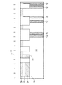
12 トレンチ
14 バルク・シリコン領域
20 シリコン・オン・インシュレータ(SOI)領域
22 シリコン層
24 埋め込み絶縁体
30 パッド層
40 ハードマスク層
42 エッチング
50 時限エッチング
60 エッチング
70 STI材料
72 STI
100 半導体デバイス
Claims (9)
- シリコン・オン・インシュレータ(SOI)領域およびバルク・シリコン領域を含むデバイス内にシリコン・トレンチ分離部(STI)を形成する方法であって、
STIマスクを使用して最上のシリコン層の上面で停止するように、前記最上のシリコン層の上層をエッチングするステップと、
バルク・シリコン領域において当該バルク・シリコン領域に形成されるSTIに必要な深さまでエッチングし且つSOI領域の埋め込み絶縁体で停止する時限エッチングを実行するステップと、
SOI領域の前記埋め込み絶縁体を貫通してエッチングするステップと、
STIを形成するためにSTI材料を堆積するステップと、
を含む方法。 - 前記バルク・シリコン領域に形成されるSTIに必要な深さが、前記SOI領域のシリコン層および前記埋め込み絶縁体の厚さと少なくとも同じ厚さである、請求項1に記載の方法。
- さらに、ハードマスク層を堆積し、パターン化し、エッチングして前記STIマスクを形成することによって、前記STIマスクを形成するステップを含む、請求項1に記載の方法。
- 前記STIマスクのエッチング・ステップが、前記ハードマスク層と、任意の反射防止コーティング(ARC)およびパッド層のうち少なくとも1つとを貫通してエッチングすることを含む、請求項3に記載の方法。
- 前記時限エッチングのステップが、前記埋め込み絶縁体の材料に対して選択的であるエッチングレシピを使用することを含む、請求項1に記載の方法。
- 前記埋め込み絶縁体のエッチング・ステップが、前記STIマスクを除去することを含む、請求項1に記載の方法。
- さらに、最上面の上の前記STI材料を除去するために研磨するステップと、パッド層を除去するステップとを含む、請求項1に記載の方法。
- シリコン・オン・インシュレータ(SOI)領域とバルク・シリコン領域が混合したデバイスのシリコン・トレンチ分離部(STI)をエッチングする方法であって、
STIマスクを使用して最上のシリコン層の上面で停止するように、前記最上のシリコン層の上層をエッチングするステップと、
バルク・シリコン領域において当該バルク・シリコン領域に形成されるSTIに必要な深さまでエッチングし且つSOI領域の埋め込み絶縁体で停止する時限エッチングを実行するステップと、
SOI領域の前記埋め込み絶縁体を貫通してエッチングするステップと、
を含む方法。 - シリコン・オン・インシュレータ(SOI)領域およびバルク・シリコン領域を含むデバイス内にシリコン・トレンチ分離部(STI)を形成する方法であって、
STIマスクを準備するステップと、
前記SOI領域および前記バルク・シリコン領域内に前記STIを同時に形成するステップと、
を含み、前記形成ステップが、
前記STIマスクを使用して最上のシリコン層の上面で停止するように、前記最上のシリコン層の上層をエッチングするステップと、
前記バルク・シリコン領域において当該バルク・シリコン領域に形成されるSTIに必要な深さまでエッチングし、前記SOI領域の埋め込み絶縁体上で停止する時限エッチングを実行するステップと、
前記SOI領域の前記埋め込み絶縁体を貫通してエッチングするステップと、
前記STIを形成するためにSTI材料を堆積させるステップと
を含む、方法。
Applications Claiming Priority (3)
| Application Number | Priority Date | Filing Date | Title |
|---|---|---|---|
| US10/710,060 US7118986B2 (en) | 2004-06-16 | 2004-06-16 | STI formation in semiconductor device including SOI and bulk silicon regions |
| US10/710,060 | 2004-06-16 | ||
| PCT/US2005/019815 WO2006009613A2 (en) | 2004-06-16 | 2005-06-06 | Sti formation in semiconductor device including soi and bulk silicon regions |
Publications (3)
| Publication Number | Publication Date |
|---|---|
| JP2008503872A JP2008503872A (ja) | 2008-02-07 |
| JP2008503872A5 JP2008503872A5 (ja) | 2008-06-19 |
| JP5004791B2 true JP5004791B2 (ja) | 2012-08-22 |
Family
ID=35481177
Family Applications (1)
| Application Number | Title | Priority Date | Filing Date |
|---|---|---|---|
| JP2007516538A Expired - Fee Related JP5004791B2 (ja) | 2004-06-16 | 2005-06-06 | Soiおよびバルク・シリコン領域を含む半導体デバイス内のsti形成 |
Country Status (6)
| Country | Link |
|---|---|
| US (2) | US7118986B2 (ja) |
| EP (1) | EP1782473A4 (ja) |
| JP (1) | JP5004791B2 (ja) |
| CN (1) | CN100452409C (ja) |
| TW (1) | TWI405298B (ja) |
| WO (1) | WO2006009613A2 (ja) |
Families Citing this family (54)
| Publication number | Priority date | Publication date | Assignee | Title |
|---|---|---|---|---|
| US20090130826A1 (en) * | 2004-10-11 | 2009-05-21 | Samsung Electronics Co., Ltd. | Method of Forming a Semiconductor Device Having a Strained Silicon Layer on a Silicon-Germanium Layer |
| US7285480B1 (en) * | 2006-04-07 | 2007-10-23 | International Business Machines Corporation | Integrated circuit chip with FETs having mixed body thicknesses and method of manufacture thereof |
| US9391079B2 (en) | 2007-11-29 | 2016-07-12 | Zeno Semiconductor, Inc. | Compact semiconductor memory device having reduced number of contacts, methods of operating and methods of making |
| US8194451B2 (en) | 2007-11-29 | 2012-06-05 | Zeno Semiconductor, Inc. | Memory cells, memory cell arrays, methods of using and methods of making |
| US9601493B2 (en) | 2006-11-29 | 2017-03-21 | Zeno Semiconductor, Inc | Compact semiconductor memory device having reduced number of contacts, methods of operating and methods of making |
| US8077536B2 (en) * | 2008-08-05 | 2011-12-13 | Zeno Semiconductor, Inc. | Method of operating semiconductor memory device with floating body transistor using silicon controlled rectifier principle |
| US8159868B2 (en) | 2008-08-22 | 2012-04-17 | Zeno Semiconductor, Inc. | Semiconductor memory having both volatile and non-volatile functionality including resistance change material and method of operating |
| US8514622B2 (en) | 2007-11-29 | 2013-08-20 | Zeno Semiconductor, Inc. | Compact semiconductor memory device having reduced number of contacts, methods of operating and methods of making |
| US8547756B2 (en) | 2010-10-04 | 2013-10-01 | Zeno Semiconductor, Inc. | Semiconductor memory device having an electrically floating body transistor |
| US7760548B2 (en) * | 2006-11-29 | 2010-07-20 | Yuniarto Widjaja | Semiconductor memory having both volatile and non-volatile functionality and method of operating |
| US8053327B2 (en) * | 2006-12-21 | 2011-11-08 | Globalfoundries Singapore Pte. Ltd. | Method of manufacture of an integrated circuit system with self-aligned isolation structures |
| CN101246884B (zh) * | 2007-02-12 | 2010-04-21 | 中芯国际集成电路制造(上海)有限公司 | 浅沟槽隔离区、浅沟槽隔离区掩膜版及浅沟槽隔离区制造方法 |
| US7847338B2 (en) | 2007-10-24 | 2010-12-07 | Yuniarto Widjaja | Semiconductor memory having both volatile and non-volatile functionality and method of operating |
| US10403361B2 (en) | 2007-11-29 | 2019-09-03 | Zeno Semiconductor, Inc. | Memory cells, memory cell arrays, methods of using and methods of making |
| US8174886B2 (en) | 2007-11-29 | 2012-05-08 | Zeno Semiconductor, Inc. | Semiconductor memory having electrically floating body transistor |
| US8130547B2 (en) | 2007-11-29 | 2012-03-06 | Zeno Semiconductor, Inc. | Method of maintaining the state of semiconductor memory having electrically floating body transistor |
| US8264875B2 (en) | 2010-10-04 | 2012-09-11 | Zeno Semiconducor, Inc. | Semiconductor memory device having an electrically floating body transistor |
| US8130548B2 (en) * | 2007-11-29 | 2012-03-06 | Zeno Semiconductor, Inc. | Semiconductor memory having electrically floating body transistor |
| US7871893B2 (en) * | 2008-01-28 | 2011-01-18 | International Business Machines Corporation | Method for non-selective shallow trench isolation reactive ion etch for patterning hybrid-oriented devices compatible with high-performance highly-integrated logic devices |
| US8014200B2 (en) | 2008-04-08 | 2011-09-06 | Zeno Semiconductor, Inc. | Semiconductor memory having volatile and multi-bit, non-volatile functionality and methods of operating |
| USRE47381E1 (en) | 2008-09-03 | 2019-05-07 | Zeno Semiconductor, Inc. | Forming semiconductor cells with regions of varying conductivity |
| WO2010086067A1 (en) * | 2009-01-29 | 2010-08-05 | International Business Machines Corporation | Memory transistor with a non-planar floating gate and manufacturing method thereof |
| US11908899B2 (en) | 2009-02-20 | 2024-02-20 | Zeno Semiconductor, Inc. | MOSFET and memory cell having improved drain current through back bias application |
| US8039356B2 (en) | 2010-01-20 | 2011-10-18 | International Business Machines Corporation | Through silicon via lithographic alignment and registration |
| SG10201700467UA (en) | 2010-02-07 | 2017-02-27 | Zeno Semiconductor Inc | Semiconductor memory device having electrically floating body transistor, and having both volatile and non-volatile functionality and method |
| US9922981B2 (en) | 2010-03-02 | 2018-03-20 | Zeno Semiconductor, Inc. | Compact semiconductor memory device having reduced number of contacts, methods of operating and methods of making |
| US10461084B2 (en) | 2010-03-02 | 2019-10-29 | Zeno Semiconductor, Inc. | Compact semiconductor memory device having reduced number of contacts, methods of operating and methods of making |
| US10340276B2 (en) | 2010-03-02 | 2019-07-02 | Zeno Semiconductor, Inc. | Method of maintaining the state of semiconductor memory having electrically floating body transistor |
| US8582359B2 (en) | 2010-11-16 | 2013-11-12 | Zeno Semiconductor, Inc. | Dual-port semiconductor memory and first-in first-out (FIFO) memory having electrically floating body transistor |
| US8957458B2 (en) | 2011-03-24 | 2015-02-17 | Zeno Semiconductor, Inc. | Asymmetric semiconductor memory device having electrically floating body transistor |
| CN102956818B (zh) * | 2011-08-19 | 2016-06-29 | 中芯国际集成电路制造(上海)有限公司 | 相变存储器的制造方法 |
| US9025358B2 (en) | 2011-10-13 | 2015-05-05 | Zeno Semiconductor Inc | Semiconductor memory having both volatile and non-volatile functionality comprising resistive change material and method of operating |
| US20130187159A1 (en) * | 2012-01-23 | 2013-07-25 | Infineon Technologies Ag | Integrated circuit and method of forming an integrated circuit |
| SG11201404871TA (en) | 2012-02-16 | 2014-09-26 | Zeno Semiconductor Inc | Memory cell comprising first and second transistors and methods of operating |
| US9230651B2 (en) | 2012-04-08 | 2016-01-05 | Zeno Semiconductor, Inc. | Memory device having electrically floating body transitor |
| US9208880B2 (en) | 2013-01-14 | 2015-12-08 | Zeno Semiconductor, Inc. | Content addressable memory device having electrically floating body transistor |
| US9029922B2 (en) | 2013-03-09 | 2015-05-12 | Zeno Semiconductor, Inc. | Memory device comprising electrically floating body transistor |
| US9275723B2 (en) | 2013-04-10 | 2016-03-01 | Zeno Semiconductor, Inc. | Scalable floating body memory cell for memory compilers and method of using floating body memories with memory compilers |
| US9368625B2 (en) | 2013-05-01 | 2016-06-14 | Zeno Semiconductor, Inc. | NAND string utilizing floating body memory cell |
| US9281022B2 (en) | 2013-07-10 | 2016-03-08 | Zeno Semiconductor, Inc. | Systems and methods for reducing standby power in floating body memory devices |
| US9548119B2 (en) | 2014-01-15 | 2017-01-17 | Zeno Semiconductor, Inc | Memory device comprising an electrically floating body transistor |
| US9496053B2 (en) | 2014-08-15 | 2016-11-15 | Zeno Semiconductor, Inc. | Memory device comprising electrically floating body transistor |
| US10553683B2 (en) | 2015-04-29 | 2020-02-04 | Zeno Semiconductor, Inc. | MOSFET and memory cell having improved drain current through back bias application |
| TWI694525B (zh) | 2015-04-29 | 2020-05-21 | 美商季諾半導體股份有限公司 | 通過施加回饋偏壓提高漏極電流的金屬氧化物半導體場效應電晶體(mosfet)和存儲單元 |
| US9728640B2 (en) | 2015-08-11 | 2017-08-08 | International Business Machines Corporation | Hybrid substrate engineering in CMOS finFET integration for mobility improvement |
| CN107039459A (zh) * | 2016-02-03 | 2017-08-11 | 上海硅通半导体技术有限公司 | Soi和体硅混合晶圆结构及其制备方法 |
| US10079301B2 (en) | 2016-11-01 | 2018-09-18 | Zeno Semiconductor, Inc. | Memory device comprising an electrically floating body transistor and methods of using |
| CN108389830B (zh) * | 2017-02-03 | 2020-10-16 | 联华电子股份有限公司 | 掩模的制作方法 |
| CN107946231B (zh) * | 2017-11-22 | 2020-06-16 | 上海华力微电子有限公司 | 一种FDSOI器件SOI和bulk区域浅槽形貌优化方法 |
| TWI787498B (zh) | 2018-04-18 | 2022-12-21 | 美商季諾半導體股份有限公司 | 包括電性浮體電晶體的記憶裝置 |
| US11600663B2 (en) | 2019-01-11 | 2023-03-07 | Zeno Semiconductor, Inc. | Memory cell and memory array select transistor |
| CN110416152A (zh) * | 2019-07-26 | 2019-11-05 | 上海华虹宏力半导体制造有限公司 | 深槽隔离结构及工艺方法 |
| US11289598B2 (en) | 2020-04-15 | 2022-03-29 | Globalfoundries Dresden Module One Limited Liability Company & Co. Kg | Co-integrated high voltage (HV) and medium voltage (MV) field effect transistors |
| US11495660B2 (en) | 2020-11-06 | 2022-11-08 | Globalfoundries Dresden Module One Limited Liability Company & Co. Kg | Co-integrated high voltage (HV) and medium voltage (MV) field effect transistors with defect prevention structures |
Family Cites Families (15)
| Publication number | Priority date | Publication date | Assignee | Title |
|---|---|---|---|---|
| JP3362397B2 (ja) * | 1991-03-28 | 2003-01-07 | ソニー株式会社 | ポリッシュによる平坦化工程を含む電子装置の製造方法 |
| US5795810A (en) * | 1995-03-29 | 1998-08-18 | Texas Instruments Incorporated | Deep mesa isolation in SOI |
| US5894152A (en) * | 1997-06-18 | 1999-04-13 | International Business Machines Corporation | SOI/bulk hybrid substrate and method of forming the same |
| JP4776752B2 (ja) * | 2000-04-19 | 2011-09-21 | ルネサスエレクトロニクス株式会社 | 半導体装置 |
| US6350653B1 (en) * | 2000-10-12 | 2002-02-26 | International Business Machines Corporation | Embedded DRAM on silicon-on-insulator substrate |
| US6627484B1 (en) | 2000-11-13 | 2003-09-30 | Advanced Micro Devices, Inc. | Method of forming a buried interconnect on a semiconductor on insulator wafer and a device including a buried interconnect |
| JP4322453B2 (ja) * | 2001-09-27 | 2009-09-02 | 株式会社東芝 | 半導体装置およびその製造方法 |
| JP3825688B2 (ja) * | 2001-12-25 | 2006-09-27 | 株式会社東芝 | 半導体装置の製造方法 |
| JP2003203967A (ja) * | 2001-12-28 | 2003-07-18 | Toshiba Corp | 部分soiウェーハの製造方法、半導体装置及びその製造方法 |
| JP2003243528A (ja) * | 2002-02-13 | 2003-08-29 | Toshiba Corp | 半導体装置 |
| JP3974542B2 (ja) * | 2003-03-17 | 2007-09-12 | 株式会社東芝 | 半導体基板の製造方法および半導体装置の製造方法 |
| US6825545B2 (en) * | 2003-04-03 | 2004-11-30 | International Business Machines Corporation | On chip decap trench capacitor (DTC) for ultra high performance silicon on insulator (SOI) systems microprocessors |
| JP2005072084A (ja) * | 2003-08-28 | 2005-03-17 | Toshiba Corp | 半導体装置及びその製造方法 |
| JP2005244020A (ja) * | 2004-02-27 | 2005-09-08 | Toshiba Corp | 半導体装置及びその製造方法 |
| US7229877B2 (en) * | 2004-11-17 | 2007-06-12 | International Business Machines Corporation | Trench capacitor with hybrid surface orientation substrate |
-
2004
- 2004-06-16 US US10/710,060 patent/US7118986B2/en not_active Expired - Fee Related
-
2005
- 2005-06-06 JP JP2007516538A patent/JP5004791B2/ja not_active Expired - Fee Related
- 2005-06-06 CN CNB2005800153951A patent/CN100452409C/zh not_active Expired - Fee Related
- 2005-06-06 EP EP05757090A patent/EP1782473A4/en not_active Withdrawn
- 2005-06-06 WO PCT/US2005/019815 patent/WO2006009613A2/en active Application Filing
- 2005-06-10 TW TW094119364A patent/TWI405298B/zh not_active IP Right Cessation
-
2006
- 2006-06-21 US US11/425,467 patent/US7394131B2/en not_active Expired - Fee Related
Also Published As
| Publication number | Publication date |
|---|---|
| US7118986B2 (en) | 2006-10-10 |
| EP1782473A2 (en) | 2007-05-09 |
| US7394131B2 (en) | 2008-07-01 |
| JP2008503872A (ja) | 2008-02-07 |
| WO2006009613A2 (en) | 2006-01-26 |
| WO2006009613A3 (en) | 2006-04-13 |
| CN1954435A (zh) | 2007-04-25 |
| TW200601489A (en) | 2006-01-01 |
| CN100452409C (zh) | 2009-01-14 |
| US20060244093A1 (en) | 2006-11-02 |
| TWI405298B (zh) | 2013-08-11 |
| EP1782473A4 (en) | 2010-03-17 |
| US20050282392A1 (en) | 2005-12-22 |
Similar Documents
| Publication | Publication Date | Title |
|---|---|---|
| JP5004791B2 (ja) | Soiおよびバルク・シリコン領域を含む半導体デバイス内のsti形成 | |
| US7807532B2 (en) | Method and structure for self aligned formation of a gate polysilicon layer | |
| US5989977A (en) | Shallow trench isolation process | |
| US5960299A (en) | Method of fabricating a shallow-trench isolation structure in integrated circuit | |
| US5966614A (en) | Silicon nitride-free isolation methods for integrated circuits | |
| US6071792A (en) | Methods of forming shallow trench isolation regions using plasma deposition techniques | |
| US6015757A (en) | Method of oxide etching with high selectivity to silicon nitride by using polysilicon layer | |
| US8669152B2 (en) | Methods of manufacturing semiconductor devices | |
| US5554560A (en) | Method for forming a planar field oxide (fox) on substrates for integrated circuit | |
| US6599813B2 (en) | Method of forming shallow trench isolation for thin silicon-on-insulator substrates | |
| US6093618A (en) | Method of fabricating a shallow trench isolation structure | |
| JP4037597B2 (ja) | トレンチ素子分離方法 | |
| US6410403B1 (en) | Method for planarizing a shallow trench isolation | |
| US20080081433A1 (en) | Method for Forming a Shallow Trench Isolation Structure | |
| US6191000B1 (en) | Shallow trench isolation method used in a semiconductor wafer | |
| US6391739B1 (en) | Process of eliminating a shallow trench isolation divot | |
| US20010012675A1 (en) | Shallow trench isolation process | |
| KR100968305B1 (ko) | Soi 및 벌크 실리콘 영역을 포함하는 반도체 장치 내의sti 형성 | |
| US6281093B1 (en) | Method to reduce trench cone formation in the fabrication of shallow trench isolations | |
| KR100455726B1 (ko) | 반도체 소자의 소자분리막 형성방법 | |
| JP2006108423A (ja) | 素子分離構造部の製造方法 | |
| KR100575080B1 (ko) | 소자 분리막 형성 방법 | |
| KR100499409B1 (ko) | 반도체소자의 소자분리막 형성방법 | |
| KR19990055757A (ko) | 반도체 소자의 소자분리막 형성방법 | |
| US20070148905A1 (en) | Method of forming a trench isolation layer in a semiconductor device |
Legal Events
| Date | Code | Title | Description |
|---|---|---|---|
| A521 | Request for written amendment filed |
Free format text: JAPANESE INTERMEDIATE CODE: A523 Effective date: 20080424 |
|
| A621 | Written request for application examination |
Free format text: JAPANESE INTERMEDIATE CODE: A621 Effective date: 20080424 |
|
| A977 | Report on retrieval |
Free format text: JAPANESE INTERMEDIATE CODE: A971007 Effective date: 20111226 |
|
| A131 | Notification of reasons for refusal |
Free format text: JAPANESE INTERMEDIATE CODE: A131 Effective date: 20120110 |
|
| A521 | Request for written amendment filed |
Free format text: JAPANESE INTERMEDIATE CODE: A523 Effective date: 20120405 |
|
| TRDD | Decision of grant or rejection written | ||
| A01 | Written decision to grant a patent or to grant a registration (utility model) |
Free format text: JAPANESE INTERMEDIATE CODE: A01 Effective date: 20120508 |
|
| A01 | Written decision to grant a patent or to grant a registration (utility model) |
Free format text: JAPANESE INTERMEDIATE CODE: A01 |
|
| A61 | First payment of annual fees (during grant procedure) |
Free format text: JAPANESE INTERMEDIATE CODE: A61 Effective date: 20120522 |
|
| FPAY | Renewal fee payment (event date is renewal date of database) |
Free format text: PAYMENT UNTIL: 20150601 Year of fee payment: 3 |
|
| R150 | Certificate of patent or registration of utility model |
Free format text: JAPANESE INTERMEDIATE CODE: R150 |
|
| R250 | Receipt of annual fees |
Free format text: JAPANESE INTERMEDIATE CODE: R250 |
|
| R250 | Receipt of annual fees |
Free format text: JAPANESE INTERMEDIATE CODE: R250 |
|
| LAPS | Cancellation because of no payment of annual fees |