JP4903987B2 - 半導体装置の製造方法 - Google Patents
半導体装置の製造方法 Download PDFInfo
- Publication number
- JP4903987B2 JP4903987B2 JP2004079597A JP2004079597A JP4903987B2 JP 4903987 B2 JP4903987 B2 JP 4903987B2 JP 2004079597 A JP2004079597 A JP 2004079597A JP 2004079597 A JP2004079597 A JP 2004079597A JP 4903987 B2 JP4903987 B2 JP 4903987B2
- Authority
- JP
- Japan
- Prior art keywords
- semiconductor device
- mold
- curable liquid
- liquid silicone
- manufacturing
- Prior art date
- Legal status (The legal status is an assumption and is not a legal conclusion. Google has not performed a legal analysis and makes no representation as to the accuracy of the status listed.)
- Expired - Lifetime
Links
- 239000004065 semiconductor Substances 0.000 title claims description 162
- 238000004519 manufacturing process Methods 0.000 title claims description 20
- 229920001296 polysiloxane Polymers 0.000 claims description 69
- 239000000203 mixture Substances 0.000 claims description 60
- 239000007788 liquid Substances 0.000 claims description 46
- 238000000465 moulding Methods 0.000 claims description 34
- 238000000034 method Methods 0.000 claims description 31
- 238000000748 compression moulding Methods 0.000 claims description 22
- 238000006459 hydrosilylation reaction Methods 0.000 claims description 15
- 238000005259 measurement Methods 0.000 claims description 8
- 238000007789 sealing Methods 0.000 description 44
- 229920005989 resin Polymers 0.000 description 32
- 239000011347 resin Substances 0.000 description 32
- 229920002379 silicone rubber Polymers 0.000 description 15
- 230000000052 comparative effect Effects 0.000 description 11
- 239000004944 Liquid Silicone Rubber Substances 0.000 description 8
- 239000003822 epoxy resin Substances 0.000 description 7
- 229920000647 polyepoxide Polymers 0.000 description 7
- 239000004945 silicone rubber Substances 0.000 description 7
- 238000004804 winding Methods 0.000 description 7
- 239000003795 chemical substances by application Substances 0.000 description 5
- 230000006835 compression Effects 0.000 description 4
- 238000007906 compression Methods 0.000 description 4
- 238000005520 cutting process Methods 0.000 description 4
- 239000000463 material Substances 0.000 description 4
- 229910000679 solder Inorganic materials 0.000 description 4
- 238000011156 evaluation Methods 0.000 description 3
- 239000010410 layer Substances 0.000 description 3
- -1 polytetrafluoroethylene Polymers 0.000 description 3
- 239000011800 void material Substances 0.000 description 3
- RYGMFSIKBFXOCR-UHFFFAOYSA-N Copper Chemical compound [Cu] RYGMFSIKBFXOCR-UHFFFAOYSA-N 0.000 description 2
- 239000004743 Polypropylene Substances 0.000 description 2
- 239000011889 copper foil Substances 0.000 description 2
- 229920001971 elastomer Polymers 0.000 description 2
- 229920000840 ethylene tetrafluoroethylene copolymer Polymers 0.000 description 2
- 230000002093 peripheral effect Effects 0.000 description 2
- BASFCYQUMIYNBI-UHFFFAOYSA-N platinum Chemical compound [Pt] BASFCYQUMIYNBI-UHFFFAOYSA-N 0.000 description 2
- 229920000139 polyethylene terephthalate Polymers 0.000 description 2
- 239000005020 polyethylene terephthalate Substances 0.000 description 2
- 229920001343 polytetrafluoroethylene Polymers 0.000 description 2
- 239000004810 polytetrafluoroethylene Substances 0.000 description 2
- 238000004382 potting Methods 0.000 description 2
- 238000007650 screen-printing Methods 0.000 description 2
- 238000001179 sorption measurement Methods 0.000 description 2
- 229920001875 Ebonite Polymers 0.000 description 1
- 239000002033 PVDF binder Substances 0.000 description 1
- 239000000654 additive Substances 0.000 description 1
- 230000000996 additive effect Effects 0.000 description 1
- 239000012790 adhesive layer Substances 0.000 description 1
- 125000003342 alkenyl group Chemical group 0.000 description 1
- XAGFODPZIPBFFR-UHFFFAOYSA-N aluminium Chemical compound [Al] XAGFODPZIPBFFR-UHFFFAOYSA-N 0.000 description 1
- 229910052782 aluminium Inorganic materials 0.000 description 1
- 238000007664 blowing Methods 0.000 description 1
- 239000003054 catalyst Substances 0.000 description 1
- 239000000919 ceramic Substances 0.000 description 1
- 238000004140 cleaning Methods 0.000 description 1
- 229920006026 co-polymeric resin Polymers 0.000 description 1
- 238000006482 condensation reaction Methods 0.000 description 1
- 239000004020 conductor Substances 0.000 description 1
- 238000011109 contamination Methods 0.000 description 1
- 230000007547 defect Effects 0.000 description 1
- 230000005611 electricity Effects 0.000 description 1
- 239000000945 filler Substances 0.000 description 1
- PCHJSUWPFVWCPO-UHFFFAOYSA-N gold Chemical compound [Au] PCHJSUWPFVWCPO-UHFFFAOYSA-N 0.000 description 1
- 229910052737 gold Inorganic materials 0.000 description 1
- 239000010931 gold Substances 0.000 description 1
- 238000010438 heat treatment Methods 0.000 description 1
- 125000004435 hydrogen atom Chemical group [H]* 0.000 description 1
- 230000007257 malfunction Effects 0.000 description 1
- 229920006136 organohydrogenpolysiloxane Polymers 0.000 description 1
- 239000000049 pigment Substances 0.000 description 1
- 229910052697 platinum Inorganic materials 0.000 description 1
- 229920001721 polyimide Polymers 0.000 description 1
- 239000009719 polyimide resin Substances 0.000 description 1
- 229920001155 polypropylene Polymers 0.000 description 1
- 229920002981 polyvinylidene fluoride Polymers 0.000 description 1
- 239000003223 protective agent Substances 0.000 description 1
- 238000004080 punching Methods 0.000 description 1
- 238000007348 radical reaction Methods 0.000 description 1
- 239000002683 reaction inhibitor Substances 0.000 description 1
- 230000003014 reinforcing effect Effects 0.000 description 1
- 239000011342 resin composition Substances 0.000 description 1
- 239000003566 sealing material Substances 0.000 description 1
- 229920002050 silicone resin Polymers 0.000 description 1
- 230000003068 static effect Effects 0.000 description 1
- BFKJFAAPBSQJPD-UHFFFAOYSA-N tetrafluoroethene Chemical group FC(F)=C(F)F BFKJFAAPBSQJPD-UHFFFAOYSA-N 0.000 description 1
- 238000001721 transfer moulding Methods 0.000 description 1
- 238000011179 visual inspection Methods 0.000 description 1
Images


Classifications
-
- H—ELECTRICITY
- H01—ELECTRIC ELEMENTS
- H01L—SEMICONDUCTOR DEVICES NOT COVERED BY CLASS H10
- H01L21/00—Processes or apparatus adapted for the manufacture or treatment of semiconductor or solid state devices or of parts thereof
- H01L21/02—Manufacture or treatment of semiconductor devices or of parts thereof
- H01L21/04—Manufacture or treatment of semiconductor devices or of parts thereof the devices having at least one potential-jump barrier or surface barrier, e.g. PN junction, depletion layer or carrier concentration layer
- H01L21/50—Assembly of semiconductor devices using processes or apparatus not provided for in a single one of the subgroups H01L21/06 - H01L21/326, e.g. sealing of a cap to a base of a container
- H01L21/56—Encapsulations, e.g. encapsulation layers, coatings
- H01L21/565—Moulds
- H01L21/566—Release layers for moulds, e.g. release layers, layers against residue during moulding
-
- H—ELECTRICITY
- H01—ELECTRIC ELEMENTS
- H01L—SEMICONDUCTOR DEVICES NOT COVERED BY CLASS H10
- H01L23/00—Details of semiconductor or other solid state devices
- H01L23/28—Encapsulations, e.g. encapsulating layers, coatings, e.g. for protection
- H01L23/29—Encapsulations, e.g. encapsulating layers, coatings, e.g. for protection characterised by the material, e.g. carbon
-
- H—ELECTRICITY
- H01—ELECTRIC ELEMENTS
- H01L—SEMICONDUCTOR DEVICES NOT COVERED BY CLASS H10
- H01L21/00—Processes or apparatus adapted for the manufacture or treatment of semiconductor or solid state devices or of parts thereof
- H01L21/02—Manufacture or treatment of semiconductor devices or of parts thereof
- H01L21/04—Manufacture or treatment of semiconductor devices or of parts thereof the devices having at least one potential-jump barrier or surface barrier, e.g. PN junction, depletion layer or carrier concentration layer
- H01L21/50—Assembly of semiconductor devices using processes or apparatus not provided for in a single one of the subgroups H01L21/06 - H01L21/326, e.g. sealing of a cap to a base of a container
- H01L21/56—Encapsulations, e.g. encapsulation layers, coatings
-
- H—ELECTRICITY
- H01—ELECTRIC ELEMENTS
- H01L—SEMICONDUCTOR DEVICES NOT COVERED BY CLASS H10
- H01L23/00—Details of semiconductor or other solid state devices
- H01L23/28—Encapsulations, e.g. encapsulating layers, coatings, e.g. for protection
- H01L23/29—Encapsulations, e.g. encapsulating layers, coatings, e.g. for protection characterised by the material, e.g. carbon
- H01L23/293—Organic, e.g. plastic
- H01L23/296—Organo-silicon compounds
-
- H—ELECTRICITY
- H01—ELECTRIC ELEMENTS
- H01L—SEMICONDUCTOR DEVICES NOT COVERED BY CLASS H10
- H01L24/00—Arrangements for connecting or disconnecting semiconductor or solid-state bodies; Methods or apparatus related thereto
- H01L24/93—Batch processes
- H01L24/95—Batch processes at chip-level, i.e. with connecting carried out on a plurality of singulated devices, i.e. on diced chips
- H01L24/97—Batch processes at chip-level, i.e. with connecting carried out on a plurality of singulated devices, i.e. on diced chips the devices being connected to a common substrate, e.g. interposer, said common substrate being separable into individual assemblies after connecting
-
- H—ELECTRICITY
- H01—ELECTRIC ELEMENTS
- H01L—SEMICONDUCTOR DEVICES NOT COVERED BY CLASS H10
- H01L2224/00—Indexing scheme for arrangements for connecting or disconnecting semiconductor or solid-state bodies and methods related thereto as covered by H01L24/00
- H01L2224/01—Means for bonding being attached to, or being formed on, the surface to be connected, e.g. chip-to-package, die-attach, "first-level" interconnects; Manufacturing methods related thereto
- H01L2224/10—Bump connectors; Manufacturing methods related thereto
- H01L2224/15—Structure, shape, material or disposition of the bump connectors after the connecting process
- H01L2224/16—Structure, shape, material or disposition of the bump connectors after the connecting process of an individual bump connector
- H01L2224/161—Disposition
- H01L2224/16151—Disposition the bump connector connecting between a semiconductor or solid-state body and an item not being a semiconductor or solid-state body, e.g. chip-to-substrate, chip-to-passive
- H01L2224/16221—Disposition the bump connector connecting between a semiconductor or solid-state body and an item not being a semiconductor or solid-state body, e.g. chip-to-substrate, chip-to-passive the body and the item being stacked
- H01L2224/16225—Disposition the bump connector connecting between a semiconductor or solid-state body and an item not being a semiconductor or solid-state body, e.g. chip-to-substrate, chip-to-passive the body and the item being stacked the item being non-metallic, e.g. insulating substrate with or without metallisation
-
- H—ELECTRICITY
- H01—ELECTRIC ELEMENTS
- H01L—SEMICONDUCTOR DEVICES NOT COVERED BY CLASS H10
- H01L2224/00—Indexing scheme for arrangements for connecting or disconnecting semiconductor or solid-state bodies and methods related thereto as covered by H01L24/00
- H01L2224/01—Means for bonding being attached to, or being formed on, the surface to be connected, e.g. chip-to-package, die-attach, "first-level" interconnects; Manufacturing methods related thereto
- H01L2224/26—Layer connectors, e.g. plate connectors, solder or adhesive layers; Manufacturing methods related thereto
- H01L2224/31—Structure, shape, material or disposition of the layer connectors after the connecting process
- H01L2224/32—Structure, shape, material or disposition of the layer connectors after the connecting process of an individual layer connector
- H01L2224/321—Disposition
- H01L2224/32151—Disposition the layer connector connecting between a semiconductor or solid-state body and an item not being a semiconductor or solid-state body, e.g. chip-to-substrate, chip-to-passive
- H01L2224/32221—Disposition the layer connector connecting between a semiconductor or solid-state body and an item not being a semiconductor or solid-state body, e.g. chip-to-substrate, chip-to-passive the body and the item being stacked
- H01L2224/32225—Disposition the layer connector connecting between a semiconductor or solid-state body and an item not being a semiconductor or solid-state body, e.g. chip-to-substrate, chip-to-passive the body and the item being stacked the item being non-metallic, e.g. insulating substrate with or without metallisation
-
- H—ELECTRICITY
- H01—ELECTRIC ELEMENTS
- H01L—SEMICONDUCTOR DEVICES NOT COVERED BY CLASS H10
- H01L2224/00—Indexing scheme for arrangements for connecting or disconnecting semiconductor or solid-state bodies and methods related thereto as covered by H01L24/00
- H01L2224/01—Means for bonding being attached to, or being formed on, the surface to be connected, e.g. chip-to-package, die-attach, "first-level" interconnects; Manufacturing methods related thereto
- H01L2224/42—Wire connectors; Manufacturing methods related thereto
- H01L2224/44—Structure, shape, material or disposition of the wire connectors prior to the connecting process
- H01L2224/45—Structure, shape, material or disposition of the wire connectors prior to the connecting process of an individual wire connector
- H01L2224/45001—Core members of the connector
- H01L2224/45099—Material
- H01L2224/451—Material with a principal constituent of the material being a metal or a metalloid, e.g. boron (B), silicon (Si), germanium (Ge), arsenic (As), antimony (Sb), tellurium (Te) and polonium (Po), and alloys thereof
- H01L2224/45138—Material with a principal constituent of the material being a metal or a metalloid, e.g. boron (B), silicon (Si), germanium (Ge), arsenic (As), antimony (Sb), tellurium (Te) and polonium (Po), and alloys thereof the principal constituent melting at a temperature of greater than or equal to 950°C and less than 1550°C
- H01L2224/45144—Gold (Au) as principal constituent
-
- H—ELECTRICITY
- H01—ELECTRIC ELEMENTS
- H01L—SEMICONDUCTOR DEVICES NOT COVERED BY CLASS H10
- H01L2224/00—Indexing scheme for arrangements for connecting or disconnecting semiconductor or solid-state bodies and methods related thereto as covered by H01L24/00
- H01L2224/01—Means for bonding being attached to, or being formed on, the surface to be connected, e.g. chip-to-package, die-attach, "first-level" interconnects; Manufacturing methods related thereto
- H01L2224/42—Wire connectors; Manufacturing methods related thereto
- H01L2224/47—Structure, shape, material or disposition of the wire connectors after the connecting process
- H01L2224/48—Structure, shape, material or disposition of the wire connectors after the connecting process of an individual wire connector
- H01L2224/4805—Shape
- H01L2224/4809—Loop shape
- H01L2224/48091—Arched
-
- H—ELECTRICITY
- H01—ELECTRIC ELEMENTS
- H01L—SEMICONDUCTOR DEVICES NOT COVERED BY CLASS H10
- H01L2224/00—Indexing scheme for arrangements for connecting or disconnecting semiconductor or solid-state bodies and methods related thereto as covered by H01L24/00
- H01L2224/01—Means for bonding being attached to, or being formed on, the surface to be connected, e.g. chip-to-package, die-attach, "first-level" interconnects; Manufacturing methods related thereto
- H01L2224/42—Wire connectors; Manufacturing methods related thereto
- H01L2224/47—Structure, shape, material or disposition of the wire connectors after the connecting process
- H01L2224/48—Structure, shape, material or disposition of the wire connectors after the connecting process of an individual wire connector
- H01L2224/481—Disposition
- H01L2224/48151—Connecting between a semiconductor or solid-state body and an item not being a semiconductor or solid-state body, e.g. chip-to-substrate, chip-to-passive
- H01L2224/48221—Connecting between a semiconductor or solid-state body and an item not being a semiconductor or solid-state body, e.g. chip-to-substrate, chip-to-passive the body and the item being stacked
- H01L2224/48225—Connecting between a semiconductor or solid-state body and an item not being a semiconductor or solid-state body, e.g. chip-to-substrate, chip-to-passive the body and the item being stacked the item being non-metallic, e.g. insulating substrate with or without metallisation
- H01L2224/48227—Connecting between a semiconductor or solid-state body and an item not being a semiconductor or solid-state body, e.g. chip-to-substrate, chip-to-passive the body and the item being stacked the item being non-metallic, e.g. insulating substrate with or without metallisation connecting the wire to a bond pad of the item
-
- H—ELECTRICITY
- H01—ELECTRIC ELEMENTS
- H01L—SEMICONDUCTOR DEVICES NOT COVERED BY CLASS H10
- H01L2224/00—Indexing scheme for arrangements for connecting or disconnecting semiconductor or solid-state bodies and methods related thereto as covered by H01L24/00
- H01L2224/73—Means for bonding being of different types provided for in two or more of groups H01L2224/10, H01L2224/18, H01L2224/26, H01L2224/34, H01L2224/42, H01L2224/50, H01L2224/63, H01L2224/71
- H01L2224/732—Location after the connecting process
- H01L2224/73201—Location after the connecting process on the same surface
- H01L2224/73203—Bump and layer connectors
- H01L2224/73204—Bump and layer connectors the bump connector being embedded into the layer connector
-
- H—ELECTRICITY
- H01—ELECTRIC ELEMENTS
- H01L—SEMICONDUCTOR DEVICES NOT COVERED BY CLASS H10
- H01L23/00—Details of semiconductor or other solid state devices
- H01L23/28—Encapsulations, e.g. encapsulating layers, coatings, e.g. for protection
- H01L23/31—Encapsulations, e.g. encapsulating layers, coatings, e.g. for protection characterised by the arrangement or shape
- H01L23/3107—Encapsulations, e.g. encapsulating layers, coatings, e.g. for protection characterised by the arrangement or shape the device being completely enclosed
- H01L23/3121—Encapsulations, e.g. encapsulating layers, coatings, e.g. for protection characterised by the arrangement or shape the device being completely enclosed a substrate forming part of the encapsulation
-
- H—ELECTRICITY
- H01—ELECTRIC ELEMENTS
- H01L—SEMICONDUCTOR DEVICES NOT COVERED BY CLASS H10
- H01L2924/00—Indexing scheme for arrangements or methods for connecting or disconnecting semiconductor or solid-state bodies as covered by H01L24/00
- H01L2924/10—Details of semiconductor or other solid state devices to be connected
- H01L2924/11—Device type
- H01L2924/12—Passive devices, e.g. 2 terminal devices
- H01L2924/1204—Optical Diode
- H01L2924/12042—LASER
-
- H—ELECTRICITY
- H01—ELECTRIC ELEMENTS
- H01L—SEMICONDUCTOR DEVICES NOT COVERED BY CLASS H10
- H01L2924/00—Indexing scheme for arrangements or methods for connecting or disconnecting semiconductor or solid-state bodies as covered by H01L24/00
- H01L2924/15—Details of package parts other than the semiconductor or other solid state devices to be connected
- H01L2924/151—Die mounting substrate
- H01L2924/153—Connection portion
- H01L2924/1531—Connection portion the connection portion being formed only on the surface of the substrate opposite to the die mounting surface
- H01L2924/15311—Connection portion the connection portion being formed only on the surface of the substrate opposite to the die mounting surface being a ball array, e.g. BGA
-
- H—ELECTRICITY
- H01—ELECTRIC ELEMENTS
- H01L—SEMICONDUCTOR DEVICES NOT COVERED BY CLASS H10
- H01L2924/00—Indexing scheme for arrangements or methods for connecting or disconnecting semiconductor or solid-state bodies as covered by H01L24/00
- H01L2924/15—Details of package parts other than the semiconductor or other solid state devices to be connected
- H01L2924/181—Encapsulation
Description
また、本発明の半導体装置は、上記の方法により製造されたことを特徴とする。
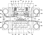
本方法では、半導体装置を金型中に載置して、該金型と該半導体装置との間に供給した硬化性液状シリコーン組成物を所定の成形温度で圧縮成形することにより、半導体装置をシリコーン硬化物で封止する。このような金型を有する圧縮成形機としては、一般に使用されている圧縮成形機を用いることができ、半導体装置を挟持して、金型と半導体装置のキャビティに供給された硬化性液状シリコーン組成物を圧縮成形することのできる上型と下型、これらを加圧するためのクランプ、硬化性液状シリコーン組成物を加熱により硬化させるためのヒーター等を備えていればよい。このような圧縮成形機としては、特開平8−244064号公報、特開平11−77733号公報、あるいは特開2000−277551号公報に記載されている圧縮成形機が例示され、特に、装置が簡単であることから、特開2000−277551号公報により記載されている圧縮成形機であることが好ましい。
硬化性液状シリコーン組成物の室温(25℃)における粘度を、E型回転粘度計(株式会社トキメック社製、コーン:3°、28mmφ)により測定した。
硬化性液状シリコーン組成物を、キュラストメーター(オリエンテック社製のJSRキュラストメーターIII―NPS型)を用いて、各成形温度(70℃、120℃)における、トルク値(kgf・cm)と経過時間(分)を測定した。なお、測定は、硬化性液状シリコーン組成物5mlを下側ダイスに載せ、上側ダイスが閉まった時点を測定開始とした。なお、ゴム用R型ダイスを用い、振幅角度は3°、振動数は100回/分、トルクレンジを最小の10kgf・cmにして測定した。
硬化性液状シリコーン組成物を120℃で30kgf/cm2の荷重を掛けて5分間圧縮成形した後、さらに120℃のオーブン中で1時間加熱処理することによりシリコーン硬化物を作製した。このシリコーン硬化物の25℃における複素弾性率を、粘弾性測定機(せん断周波数:1Hz、歪み率:0.5%)により測定した。
[成形物外観]
シリコーン硬化物あるいはエポキシ樹脂硬化物で封止した半導体装置について、中心部の厚みと外周部の厚みの差が5%未満であるものを○、5%以上、10%未満である場合を△、10%以上である場合を×とした。
目視により、シリコーン硬化物あるいはエポキシ樹脂硬化物で封止した半導体装置の表面を観察し、ボイドがなく末端まで均一に充填されているものを○、少しでもボイドや未未充填部分があるものを×とした。
半導体装置を個片に切断する前の、シリコーン硬化物あるいはエポキシ樹脂硬化物で封止した回路基板の長辺側を固定した時の他端長辺側の高さを測定し、これを反りとして示した。

図3に示す半導体装置を作製した。すなわち、70mm×160mmサイズのBT樹脂製回路基板12(厚さ200μmのBT樹脂フィルムの片面に、厚さ17μmのエポキシ樹脂製接着剤層を介して厚さ18μmの銅箔が積層されており、この銅箔により回路パターンが形成され、この回路パターンのワイヤボンディングするための部分を除き、回路基板12の表面は感光性ソルダーマスクにより被覆されている。)に厚さ35μmのエポキシ樹脂製ダイボンド剤層を介して8mm×14mmサイズの半導体チップ10を接合した。次に、この半導体チップ10のバンプ(図示せず)と回路パターンとを電気的に接続するため48本の金製ボンディングワイヤによりワイヤボンディングした。この回路基板12には、合わせて54個の半導体チップが18個ずつ3ブロックに分けて実装されており、それぞれ回路パターンにワイヤーボンディングされている。
実施例1において、ヒドロシリル化反応硬化性液状シリコーンゴム組成物(A)の代わりにヒドロシリル化反応硬化性液状シリコーンゴム組成物(B)を用いた以外は実施例1と同様にして半導体装置を作製した。この半導体装置の特性を表2に示した。
実施例1において、ヒドロシリル化反応硬化性シリコーンゴム組成物(A)の代わりにヒドロシリル化反応硬化性シリコーンゴム組成物(C)を用い、70℃で35kgf/cm2の荷重をかけて15分間圧縮成形した以外は、実施例1と同様にして半導体装置を作製した。この半導体装置の特性を表2に示した。
比較例1において、ヒドロシリル化反応硬化性液状シリコーンゴム組成物(C)の代わりにヒドロシリル化反応硬化性液状シリコーンゴム組成物(D)を用いた以外は比較例1と同様にして半導体装置を作製した。この半導体装置の特性を表2に示した。
実施例1において、ヒドロシリル化反応硬化性シリコーンゴム組成物(A)の代わりにヒドロシリル化反応硬化性シリコーンゴム組成物(C)を用い、120℃で50kgf/cm2の荷重をかけて3分間圧縮成形した以外は、実施例1と同様にして半導体装置を作製した。この半導体装置の特性を表2に示した。
比較例3において、ヒドロシリル化反応硬化性液状シリコーンゴム組成物(C)の代わりにヒドロシリル化反応硬化性液状シリコーンゴム組成物(D)を用いた以外は比較例3と同様にして半導体装置を作製した。この半導体装置の特性を表2に示した。
12 回路基板
14 シリコーン硬化物
16 半導体装置
20 固定プラテン
22 下型ベース
23 下型
24 ヒータ
26 下クランプストッパ
30 可動プラテン
32 上型ベース
33 上型ホルダ
34 上型
34a キャビティ凹部
36 クランパ
36a、36b エア孔
37 スプリング
38 ヒータ
39 上クランプストッパ
40a、40b 剥離性フィルム
42a、42b 供給ロール
44a、44b 巻取りロール
46 ガイドローラ
48 静電除去装置
50 硬化性液状シリコーン組成物
70 シリコーン硬化物で封止した半導体装置
72 シリコーン硬化物
Claims (7)
- 半導体装置を金型中に載置して、該金型と該半導体装置との間に供給したヒドロシリル化反応硬化性液状シリコーン組成物を50℃〜150℃の成形温度で圧縮成形することにより、複素弾性率1GPa以下のシリコーン硬化物で封止した半導体装置を製造する方法であって、前記硬化性液状シリコーン組成物が、室温(25℃)で90Pa・s以下の粘度を有し、キュラストメーターで測定した、前記成形温度における測定直後から1kgf・cmのトルクに達するまでの時間が1分以上であり、かつ1kgf・cmのトルクから5kgf・cmのトルクに達するまでの時間が1分以内であることを特徴とする半導体装置の製造方法。
- 下型に半導体装置を載置して、上型と半導体装置との間に硬化性液状シリコーン組成物を供給した後、上型と下型とで半導体装置を挟持して前記硬化性液状シリコーン組成物を圧縮成形することを特徴とする、請求項1記載の半導体装置の製造方法。
- 少なくとも2つの半導体装置をシリコーン硬化物で封止した後、個片の半導体装置に切断することを特徴とする、請求項1記載の半導体装置の製造方法。
- 半導体装置が、回路基板上に半導体チップがボンディングワイヤにより電気的に接続されているものであることを特徴とする、請求項1記載の半導体装置の製造方法。
- 回路基板の半導体チップを搭載した面に硬化性液状シリコーン組成物を供給して、半導体チップおよび該チップのボンディングワイヤーとの接続部をシリコーン硬化物で封止したことを特徴とする、請求項4記載の半導体装置の製造方法。
- 金型の内面に剥離性フィルムが密着していることを特徴とする、請求項1記載の半導体装置の製造方法。
- 剥離性フィルムがエア吸引により金型の内面に密着していることを特徴とする、請求項6記載の半導体装置の製造方法。
Priority Applications (8)
| Application Number | Priority Date | Filing Date | Title |
|---|---|---|---|
| JP2004079597A JP4903987B2 (ja) | 2004-03-19 | 2004-03-19 | 半導体装置の製造方法 |
| TW094106803A TWI383429B (zh) | 2004-03-19 | 2005-03-07 | 半導體裝置及其製法 |
| US10/599,041 US8262970B2 (en) | 2004-03-19 | 2005-03-08 | Semiconductor device and method of manufacturing thereof |
| PCT/JP2005/004410 WO2005091361A1 (en) | 2004-03-19 | 2005-03-08 | Semiconductor device and method of manufacturing thereof |
| EP05720681A EP1730775B1 (en) | 2004-03-19 | 2005-03-08 | Semiconductor device and method of manufacturing thereof |
| CNB200580008837XA CN100539092C (zh) | 2004-03-19 | 2005-03-08 | 半导体器件及其制造方法 |
| KR1020067019279A KR101168861B1 (ko) | 2004-03-19 | 2005-03-08 | 반도체 장치 및 이의 제조방법 |
| MYPI20051177A MY146873A (en) | 2004-03-19 | 2005-03-18 | Semiconductor device and method of manufacturing therof. |
Applications Claiming Priority (1)
| Application Number | Priority Date | Filing Date | Title |
|---|---|---|---|
| JP2004079597A JP4903987B2 (ja) | 2004-03-19 | 2004-03-19 | 半導体装置の製造方法 |
Publications (3)
| Publication Number | Publication Date |
|---|---|
| JP2005268565A JP2005268565A (ja) | 2005-09-29 |
| JP2005268565A5 JP2005268565A5 (ja) | 2007-03-29 |
| JP4903987B2 true JP4903987B2 (ja) | 2012-03-28 |
Family
ID=34961509
Family Applications (1)
| Application Number | Title | Priority Date | Filing Date |
|---|---|---|---|
| JP2004079597A Expired - Lifetime JP4903987B2 (ja) | 2004-03-19 | 2004-03-19 | 半導体装置の製造方法 |
Country Status (8)
| Country | Link |
|---|---|
| US (1) | US8262970B2 (ja) |
| EP (1) | EP1730775B1 (ja) |
| JP (1) | JP4903987B2 (ja) |
| KR (1) | KR101168861B1 (ja) |
| CN (1) | CN100539092C (ja) |
| MY (1) | MY146873A (ja) |
| TW (1) | TWI383429B (ja) |
| WO (1) | WO2005091361A1 (ja) |
Families Citing this family (11)
| Publication number | Priority date | Publication date | Assignee | Title |
|---|---|---|---|---|
| JP4931366B2 (ja) | 2005-04-27 | 2012-05-16 | 東レ・ダウコーニング株式会社 | 硬化性シリコーン組成物および電子部品 |
| JP5207591B2 (ja) | 2006-02-23 | 2013-06-12 | 東レ・ダウコーニング株式会社 | 半導体装置の製造方法および半導体装置 |
| JP5285846B2 (ja) | 2006-09-11 | 2013-09-11 | 東レ・ダウコーニング株式会社 | 硬化性シリコーン組成物および電子部品 |
| CN102290170A (zh) * | 2010-06-17 | 2011-12-21 | 台湾双羽电机股份有限公司 | 薄型电阻及其制造方法 |
| KR20150022990A (ko) * | 2012-06-08 | 2015-03-04 | 히타치가세이가부시끼가이샤 | 반도체 장치의 제조 방법 |
| US8997342B2 (en) * | 2012-10-15 | 2015-04-07 | Zhuhai Advanced Chip Carriers & Electronic Substrate Solutions Technologies Co. Ltd. | Method of fabrication, a multilayer electronic structure and structures in accordance with the method |
| JP2014082284A (ja) | 2012-10-15 | 2014-05-08 | Dow Corning Toray Co Ltd | 凸状硬化物及び基材を備える一体化物の製造方法 |
| US9470395B2 (en) | 2013-03-15 | 2016-10-18 | Abl Ip Holding Llc | Optic for a light source |
| CA2911523C (en) | 2013-05-10 | 2018-10-02 | Abl Ip Holding Llc | Silicone optics |
| JP6370494B2 (ja) * | 2014-09-01 | 2018-08-08 | コリア インスティチュート オブ インダストリアル テクノロジー | レドックスフロー電池用バイポーラプレートの製造方法 |
| KR101831573B1 (ko) * | 2015-03-05 | 2018-02-22 | 스미토모 베이클리트 컴퍼니 리미티드 | 봉지용 수지 조성물, 차재용 전자 제어 유닛의 제조 방법, 및 차재용 전자 제어 유닛 |
Family Cites Families (11)
| Publication number | Priority date | Publication date | Assignee | Title |
|---|---|---|---|---|
| JPH0214244A (ja) | 1988-06-30 | 1990-01-18 | Toray Dow Corning Silicone Co Ltd | 加熱硬化性オルガノポリシロキサン組成物 |
| JP3516764B2 (ja) | 1995-03-08 | 2004-04-05 | アピックヤマダ株式会社 | リリースフィルムを用いる樹脂モールド装置及び樹脂モールド方法 |
| JPH1177733A (ja) | 1997-09-01 | 1999-03-23 | Apic Yamada Kk | 樹脂モールド方法及び樹脂モールド装置 |
| US6080605A (en) * | 1998-10-06 | 2000-06-27 | Tessera, Inc. | Methods of encapsulating a semiconductor chip using a settable encapsulant |
| US6040366A (en) | 1998-02-27 | 2000-03-21 | General Electric Company | Liquid injection molding silicone elastomers having primerless adhesion |
| US6124407A (en) * | 1998-10-28 | 2000-09-26 | Dow Corning Corporation | Silicone composition, method for the preparation thereof, and silicone elastomer |
| JP3494586B2 (ja) * | 1999-03-26 | 2004-02-09 | アピックヤマダ株式会社 | 樹脂封止装置及び樹脂封止方法 |
| JP4646363B2 (ja) * | 2000-06-29 | 2011-03-09 | 東レ・ダウコーニング株式会社 | シリコーンゴム組成物 |
| JP4947858B2 (ja) * | 2001-08-21 | 2012-06-06 | 東レ・ダウコーニング株式会社 | 導電性液状シリコーンゴム組成物、導電性シリコーンゴム成形物およびその製造方法 |
| JP4061361B2 (ja) * | 2001-12-28 | 2008-03-19 | モメンティブ・パフォーマンス・マテリアルズ・ジャパン合同会社 | 付加反応型ポリオルガノシロキサン組成物 |
| WO2003102071A1 (en) * | 2002-05-31 | 2003-12-11 | Dow Corning Toray Silicone Co.,Ltd. | Thermoconductive curable liquid polymer composition and semiconductor device produced with the use of this composition |
-
2004
- 2004-03-19 JP JP2004079597A patent/JP4903987B2/ja not_active Expired - Lifetime
-
2005
- 2005-03-07 TW TW094106803A patent/TWI383429B/zh active
- 2005-03-08 CN CNB200580008837XA patent/CN100539092C/zh active Active
- 2005-03-08 WO PCT/JP2005/004410 patent/WO2005091361A1/en active Application Filing
- 2005-03-08 EP EP05720681A patent/EP1730775B1/en active Active
- 2005-03-08 KR KR1020067019279A patent/KR101168861B1/ko active IP Right Grant
- 2005-03-08 US US10/599,041 patent/US8262970B2/en active Active
- 2005-03-18 MY MYPI20051177A patent/MY146873A/en unknown
Also Published As
| Publication number | Publication date |
|---|---|
| JP2005268565A (ja) | 2005-09-29 |
| EP1730775B1 (en) | 2013-02-13 |
| US8262970B2 (en) | 2012-09-11 |
| TW200535957A (en) | 2005-11-01 |
| EP1730775A1 (en) | 2006-12-13 |
| US20070273050A1 (en) | 2007-11-29 |
| WO2005091361A1 (en) | 2005-09-29 |
| TWI383429B (zh) | 2013-01-21 |
| KR20060123643A (ko) | 2006-12-01 |
| MY146873A (en) | 2012-10-15 |
| CN100539092C (zh) | 2009-09-09 |
| KR101168861B1 (ko) | 2012-07-30 |
| CN1934699A (zh) | 2007-03-21 |
Similar Documents
| Publication | Publication Date | Title |
|---|---|---|
| JP4607429B2 (ja) | 半導体装置の製造方法および半導体装置 | |
| JP5101788B2 (ja) | 半導体装置の製造方法および半導体装置 | |
| KR101168861B1 (ko) | 반도체 장치 및 이의 제조방법 | |
| JP6062810B2 (ja) | 樹脂モールド金型及び樹脂モールド装置 | |
| US7520052B2 (en) | Method of manufacturing a semiconductor device | |
| JP2000277551A (ja) | 樹脂封止装置及び樹脂封止方法 | |
| CN108688050B (zh) | 成型模、树脂成型装置、树脂成型方法及树脂成型品的制造方法 | |
| TW201722681A (zh) | 樹脂封裝裝置以及樹脂封裝方法 | |
| JP3581814B2 (ja) | 樹脂封止方法及び樹脂封止装置 | |
| JP6598642B2 (ja) | 樹脂封止装置及び樹脂封止方法 | |
| US8084301B2 (en) | Resin sheet, circuit device and method of manufacturing the same | |
| US6544816B1 (en) | Method of encapsulating thin semiconductor chip-scale packages | |
| JP2004134591A (ja) | 半導体集積回路装置の製造方法 | |
| JP3897565B2 (ja) | 樹脂封止装置及び樹脂封止方法 | |
| JP2007036273A (ja) | 半導体集積回路装置の製造方法 | |
| JP4760876B2 (ja) | 電子装置およびその製造方法 | |
| JP6640003B2 (ja) | 樹脂封止装置及び樹脂封止方法 | |
| JP2003197680A (ja) | 半導体装置の製造方法 | |
| JP3484633B2 (ja) | 電子部品の製造方法 | |
| JP2010086996A (ja) | 回路装置の製造方法 | |
| JP5758823B2 (ja) | 電子部品の樹脂封止成形品の製造方法、圧縮成形用下金型及び樹脂封止装置 |
Legal Events
| Date | Code | Title | Description |
|---|---|---|---|
| A521 | Request for written amendment filed |
Free format text: JAPANESE INTERMEDIATE CODE: A523 Effective date: 20070207 |
|
| A621 | Written request for application examination |
Free format text: JAPANESE INTERMEDIATE CODE: A621 Effective date: 20070207 |
|
| A131 | Notification of reasons for refusal |
Free format text: JAPANESE INTERMEDIATE CODE: A131 Effective date: 20090818 |
|
| A521 | Request for written amendment filed |
Free format text: JAPANESE INTERMEDIATE CODE: A523 Effective date: 20091019 |
|
| A131 | Notification of reasons for refusal |
Free format text: JAPANESE INTERMEDIATE CODE: A131 Effective date: 20091117 |
|
| A521 | Request for written amendment filed |
Free format text: JAPANESE INTERMEDIATE CODE: A523 Effective date: 20100112 |
|
| A02 | Decision of refusal |
Free format text: JAPANESE INTERMEDIATE CODE: A02 Effective date: 20100209 |
|
| A521 | Request for written amendment filed |
Free format text: JAPANESE INTERMEDIATE CODE: A523 Effective date: 20100510 |
|
| A911 | Transfer to examiner for re-examination before appeal (zenchi) |
Free format text: JAPANESE INTERMEDIATE CODE: A911 Effective date: 20100519 |
|
| A912 | Re-examination (zenchi) completed and case transferred to appeal board |
Free format text: JAPANESE INTERMEDIATE CODE: A912 Effective date: 20100611 |
|
| A521 | Request for written amendment filed |
Free format text: JAPANESE INTERMEDIATE CODE: A821 Effective date: 20110830 |
|
| A01 | Written decision to grant a patent or to grant a registration (utility model) |
Free format text: JAPANESE INTERMEDIATE CODE: A01 |
|
| A61 | First payment of annual fees (during grant procedure) |
Free format text: JAPANESE INTERMEDIATE CODE: A61 Effective date: 20120106 |
|
| R150 | Certificate of patent or registration of utility model |
Free format text: JAPANESE INTERMEDIATE CODE: R150 Ref document number: 4903987 Country of ref document: JP Free format text: JAPANESE INTERMEDIATE CODE: R150 |
|
| FPAY | Renewal fee payment (event date is renewal date of database) |
Free format text: PAYMENT UNTIL: 20150113 Year of fee payment: 3 |
|
| R250 | Receipt of annual fees |
Free format text: JAPANESE INTERMEDIATE CODE: R250 |
|
| R250 | Receipt of annual fees |
Free format text: JAPANESE INTERMEDIATE CODE: R250 |
|
| R250 | Receipt of annual fees |
Free format text: JAPANESE INTERMEDIATE CODE: R250 |
|
| R250 | Receipt of annual fees |
Free format text: JAPANESE INTERMEDIATE CODE: R250 |
|
| R250 | Receipt of annual fees |
Free format text: JAPANESE INTERMEDIATE CODE: R250 |
|
| S111 | Request for change of ownership or part of ownership |
Free format text: JAPANESE INTERMEDIATE CODE: R313111 |
|
| R350 | Written notification of registration of transfer |
Free format text: JAPANESE INTERMEDIATE CODE: R350 |
|
| R250 | Receipt of annual fees |
Free format text: JAPANESE INTERMEDIATE CODE: R250 |
|
| R250 | Receipt of annual fees |
Free format text: JAPANESE INTERMEDIATE CODE: R250 |
|
| R250 | Receipt of annual fees |
Free format text: JAPANESE INTERMEDIATE CODE: R250 |
|
| R250 | Receipt of annual fees |
Free format text: JAPANESE INTERMEDIATE CODE: R250 |
|
| R250 | Receipt of annual fees |
Free format text: JAPANESE INTERMEDIATE CODE: R250 |