JP4828537B2 - 半導体装置 - Google Patents
半導体装置 Download PDFInfo
- Publication number
- JP4828537B2 JP4828537B2 JP2007532208A JP2007532208A JP4828537B2 JP 4828537 B2 JP4828537 B2 JP 4828537B2 JP 2007532208 A JP2007532208 A JP 2007532208A JP 2007532208 A JP2007532208 A JP 2007532208A JP 4828537 B2 JP4828537 B2 JP 4828537B2
- Authority
- JP
- Japan
- Prior art keywords
- holes
- film
- semiconductor device
- wafer
- main surface
- Prior art date
- Legal status (The legal status is an assumption and is not a legal conclusion. Google has not performed a legal analysis and makes no representation as to the accuracy of the status listed.)
- Expired - Fee Related
Links
Images


Classifications
-
- H—ELECTRICITY
- H01—ELECTRIC ELEMENTS
- H01L—SEMICONDUCTOR DEVICES NOT COVERED BY CLASS H10
- H01L25/00—Assemblies consisting of a plurality of individual semiconductor or other solid state devices ; Multistep manufacturing processes thereof
- H01L25/03—Assemblies consisting of a plurality of individual semiconductor or other solid state devices ; Multistep manufacturing processes thereof all the devices being of a type provided for in the same subgroup of groups H01L27/00 - H01L33/00, or in a single subclass of H10K, H10N, e.g. assemblies of rectifier diodes
- H01L25/04—Assemblies consisting of a plurality of individual semiconductor or other solid state devices ; Multistep manufacturing processes thereof all the devices being of a type provided for in the same subgroup of groups H01L27/00 - H01L33/00, or in a single subclass of H10K, H10N, e.g. assemblies of rectifier diodes the devices not having separate containers
- H01L25/065—Assemblies consisting of a plurality of individual semiconductor or other solid state devices ; Multistep manufacturing processes thereof all the devices being of a type provided for in the same subgroup of groups H01L27/00 - H01L33/00, or in a single subclass of H10K, H10N, e.g. assemblies of rectifier diodes the devices not having separate containers the devices being of a type provided for in group H01L27/00
- H01L25/0657—Stacked arrangements of devices
-
- H—ELECTRICITY
- H01—ELECTRIC ELEMENTS
- H01L—SEMICONDUCTOR DEVICES NOT COVERED BY CLASS H10
- H01L21/00—Processes or apparatus adapted for the manufacture or treatment of semiconductor or solid state devices or of parts thereof
- H01L21/70—Manufacture or treatment of devices consisting of a plurality of solid state components formed in or on a common substrate or of parts thereof; Manufacture of integrated circuit devices or of parts thereof
- H01L21/71—Manufacture of specific parts of devices defined in group H01L21/70
- H01L21/76—Making of isolation regions between components
- H01L21/763—Polycrystalline semiconductor regions
-
- H—ELECTRICITY
- H01—ELECTRIC ELEMENTS
- H01L—SEMICONDUCTOR DEVICES NOT COVERED BY CLASS H10
- H01L21/00—Processes or apparatus adapted for the manufacture or treatment of semiconductor or solid state devices or of parts thereof
- H01L21/70—Manufacture or treatment of devices consisting of a plurality of solid state components formed in or on a common substrate or of parts thereof; Manufacture of integrated circuit devices or of parts thereof
- H01L21/71—Manufacture of specific parts of devices defined in group H01L21/70
- H01L21/768—Applying interconnections to be used for carrying current between separate components within a device comprising conductors and dielectrics
- H01L21/76898—Applying interconnections to be used for carrying current between separate components within a device comprising conductors and dielectrics formed through a semiconductor substrate
-
- H—ELECTRICITY
- H01—ELECTRIC ELEMENTS
- H01L—SEMICONDUCTOR DEVICES NOT COVERED BY CLASS H10
- H01L21/00—Processes or apparatus adapted for the manufacture or treatment of semiconductor or solid state devices or of parts thereof
- H01L21/70—Manufacture or treatment of devices consisting of a plurality of solid state components formed in or on a common substrate or of parts thereof; Manufacture of integrated circuit devices or of parts thereof
- H01L21/77—Manufacture or treatment of devices consisting of a plurality of solid state components or integrated circuits formed in, or on, a common substrate
- H01L21/78—Manufacture or treatment of devices consisting of a plurality of solid state components or integrated circuits formed in, or on, a common substrate with subsequent division of the substrate into plural individual devices
- H01L21/82—Manufacture or treatment of devices consisting of a plurality of solid state components or integrated circuits formed in, or on, a common substrate with subsequent division of the substrate into plural individual devices to produce devices, e.g. integrated circuits, each consisting of a plurality of components
- H01L21/822—Manufacture or treatment of devices consisting of a plurality of solid state components or integrated circuits formed in, or on, a common substrate with subsequent division of the substrate into plural individual devices to produce devices, e.g. integrated circuits, each consisting of a plurality of components the substrate being a semiconductor, using silicon technology
- H01L21/8232—Field-effect technology
- H01L21/8234—MIS technology, i.e. integration processes of field effect transistors of the conductor-insulator-semiconductor type
- H01L21/8238—Complementary field-effect transistors, e.g. CMOS
- H01L21/823871—Complementary field-effect transistors, e.g. CMOS interconnection or wiring or contact manufacturing related aspects
-
- H—ELECTRICITY
- H01—ELECTRIC ELEMENTS
- H01L—SEMICONDUCTOR DEVICES NOT COVERED BY CLASS H10
- H01L21/00—Processes or apparatus adapted for the manufacture or treatment of semiconductor or solid state devices or of parts thereof
- H01L21/70—Manufacture or treatment of devices consisting of a plurality of solid state components formed in or on a common substrate or of parts thereof; Manufacture of integrated circuit devices or of parts thereof
- H01L21/77—Manufacture or treatment of devices consisting of a plurality of solid state components or integrated circuits formed in, or on, a common substrate
- H01L21/78—Manufacture or treatment of devices consisting of a plurality of solid state components or integrated circuits formed in, or on, a common substrate with subsequent division of the substrate into plural individual devices
- H01L21/82—Manufacture or treatment of devices consisting of a plurality of solid state components or integrated circuits formed in, or on, a common substrate with subsequent division of the substrate into plural individual devices to produce devices, e.g. integrated circuits, each consisting of a plurality of components
- H01L21/822—Manufacture or treatment of devices consisting of a plurality of solid state components or integrated circuits formed in, or on, a common substrate with subsequent division of the substrate into plural individual devices to produce devices, e.g. integrated circuits, each consisting of a plurality of components the substrate being a semiconductor, using silicon technology
- H01L21/8232—Field-effect technology
- H01L21/8234—MIS technology, i.e. integration processes of field effect transistors of the conductor-insulator-semiconductor type
- H01L21/8238—Complementary field-effect transistors, e.g. CMOS
- H01L21/823878—Complementary field-effect transistors, e.g. CMOS isolation region manufacturing related aspects, e.g. to avoid interaction of isolation region with adjacent structure
-
- H—ELECTRICITY
- H01—ELECTRIC ELEMENTS
- H01L—SEMICONDUCTOR DEVICES NOT COVERED BY CLASS H10
- H01L23/00—Details of semiconductor or other solid state devices
- H01L23/48—Arrangements for conducting electric current to or from the solid state body in operation, e.g. leads, terminal arrangements ; Selection of materials therefor
- H01L23/481—Internal lead connections, e.g. via connections, feedthrough structures
-
- H—ELECTRICITY
- H01—ELECTRIC ELEMENTS
- H01L—SEMICONDUCTOR DEVICES NOT COVERED BY CLASS H10
- H01L25/00—Assemblies consisting of a plurality of individual semiconductor or other solid state devices ; Multistep manufacturing processes thereof
- H01L25/50—Multistep manufacturing processes of assemblies consisting of devices, each device being of a type provided for in group H01L27/00 or H01L29/00
-
- H—ELECTRICITY
- H01—ELECTRIC ELEMENTS
- H01L—SEMICONDUCTOR DEVICES NOT COVERED BY CLASS H10
- H01L27/00—Devices consisting of a plurality of semiconductor or other solid-state components formed in or on a common substrate
- H01L27/02—Devices consisting of a plurality of semiconductor or other solid-state components formed in or on a common substrate including semiconductor components specially adapted for rectifying, oscillating, amplifying or switching and having at least one potential-jump barrier or surface barrier; including integrated passive circuit elements with at least one potential-jump barrier or surface barrier
- H01L27/0203—Particular design considerations for integrated circuits
-
- H—ELECTRICITY
- H01—ELECTRIC ELEMENTS
- H01L—SEMICONDUCTOR DEVICES NOT COVERED BY CLASS H10
- H01L2224/00—Indexing scheme for arrangements for connecting or disconnecting semiconductor or solid-state bodies and methods related thereto as covered by H01L24/00
- H01L2224/01—Means for bonding being attached to, or being formed on, the surface to be connected, e.g. chip-to-package, die-attach, "first-level" interconnects; Manufacturing methods related thereto
- H01L2224/42—Wire connectors; Manufacturing methods related thereto
- H01L2224/44—Structure, shape, material or disposition of the wire connectors prior to the connecting process
- H01L2224/45—Structure, shape, material or disposition of the wire connectors prior to the connecting process of an individual wire connector
- H01L2224/45001—Core members of the connector
- H01L2224/45099—Material
- H01L2224/451—Material with a principal constituent of the material being a metal or a metalloid, e.g. boron (B), silicon (Si), germanium (Ge), arsenic (As), antimony (Sb), tellurium (Te) and polonium (Po), and alloys thereof
- H01L2224/45138—Material with a principal constituent of the material being a metal or a metalloid, e.g. boron (B), silicon (Si), germanium (Ge), arsenic (As), antimony (Sb), tellurium (Te) and polonium (Po), and alloys thereof the principal constituent melting at a temperature of greater than or equal to 950°C and less than 1550°C
- H01L2224/45144—Gold (Au) as principal constituent
-
- H—ELECTRICITY
- H01—ELECTRIC ELEMENTS
- H01L—SEMICONDUCTOR DEVICES NOT COVERED BY CLASS H10
- H01L2224/00—Indexing scheme for arrangements for connecting or disconnecting semiconductor or solid-state bodies and methods related thereto as covered by H01L24/00
- H01L2224/01—Means for bonding being attached to, or being formed on, the surface to be connected, e.g. chip-to-package, die-attach, "first-level" interconnects; Manufacturing methods related thereto
- H01L2224/42—Wire connectors; Manufacturing methods related thereto
- H01L2224/47—Structure, shape, material or disposition of the wire connectors after the connecting process
- H01L2224/48—Structure, shape, material or disposition of the wire connectors after the connecting process of an individual wire connector
- H01L2224/481—Disposition
- H01L2224/48151—Connecting between a semiconductor or solid-state body and an item not being a semiconductor or solid-state body, e.g. chip-to-substrate, chip-to-passive
- H01L2224/48221—Connecting between a semiconductor or solid-state body and an item not being a semiconductor or solid-state body, e.g. chip-to-substrate, chip-to-passive the body and the item being stacked
- H01L2224/48225—Connecting between a semiconductor or solid-state body and an item not being a semiconductor or solid-state body, e.g. chip-to-substrate, chip-to-passive the body and the item being stacked the item being non-metallic, e.g. insulating substrate with or without metallisation
- H01L2224/48227—Connecting between a semiconductor or solid-state body and an item not being a semiconductor or solid-state body, e.g. chip-to-substrate, chip-to-passive the body and the item being stacked the item being non-metallic, e.g. insulating substrate with or without metallisation connecting the wire to a bond pad of the item
-
- H—ELECTRICITY
- H01—ELECTRIC ELEMENTS
- H01L—SEMICONDUCTOR DEVICES NOT COVERED BY CLASS H10
- H01L2224/00—Indexing scheme for arrangements for connecting or disconnecting semiconductor or solid-state bodies and methods related thereto as covered by H01L24/00
- H01L2224/01—Means for bonding being attached to, or being formed on, the surface to be connected, e.g. chip-to-package, die-attach, "first-level" interconnects; Manufacturing methods related thereto
- H01L2224/42—Wire connectors; Manufacturing methods related thereto
- H01L2224/47—Structure, shape, material or disposition of the wire connectors after the connecting process
- H01L2224/48—Structure, shape, material or disposition of the wire connectors after the connecting process of an individual wire connector
- H01L2224/484—Connecting portions
- H01L2224/48463—Connecting portions the connecting portion on the bonding area of the semiconductor or solid-state body being a ball bond
- H01L2224/48465—Connecting portions the connecting portion on the bonding area of the semiconductor or solid-state body being a ball bond the other connecting portion not on the bonding area being a wedge bond, i.e. ball-to-wedge, regular stitch
-
- H—ELECTRICITY
- H01—ELECTRIC ELEMENTS
- H01L—SEMICONDUCTOR DEVICES NOT COVERED BY CLASS H10
- H01L2225/00—Details relating to assemblies covered by the group H01L25/00 but not provided for in its subgroups
- H01L2225/03—All the devices being of a type provided for in the same subgroup of groups H01L27/00 - H01L33/648 and H10K99/00
- H01L2225/04—All the devices being of a type provided for in the same subgroup of groups H01L27/00 - H01L33/648 and H10K99/00 the devices not having separate containers
- H01L2225/065—All the devices being of a type provided for in the same subgroup of groups H01L27/00 - H01L33/648 and H10K99/00 the devices not having separate containers the devices being of a type provided for in group H01L27/00
- H01L2225/06503—Stacked arrangements of devices
- H01L2225/0651—Wire or wire-like electrical connections from device to substrate
-
- H—ELECTRICITY
- H01—ELECTRIC ELEMENTS
- H01L—SEMICONDUCTOR DEVICES NOT COVERED BY CLASS H10
- H01L2225/00—Details relating to assemblies covered by the group H01L25/00 but not provided for in its subgroups
- H01L2225/03—All the devices being of a type provided for in the same subgroup of groups H01L27/00 - H01L33/648 and H10K99/00
- H01L2225/04—All the devices being of a type provided for in the same subgroup of groups H01L27/00 - H01L33/648 and H10K99/00 the devices not having separate containers
- H01L2225/065—All the devices being of a type provided for in the same subgroup of groups H01L27/00 - H01L33/648 and H10K99/00 the devices not having separate containers the devices being of a type provided for in group H01L27/00
- H01L2225/06503—Stacked arrangements of devices
- H01L2225/06513—Bump or bump-like direct electrical connections between devices, e.g. flip-chip connection, solder bumps
-
- H—ELECTRICITY
- H01—ELECTRIC ELEMENTS
- H01L—SEMICONDUCTOR DEVICES NOT COVERED BY CLASS H10
- H01L23/00—Details of semiconductor or other solid state devices
- H01L23/28—Encapsulations, e.g. encapsulating layers, coatings, e.g. for protection
- H01L23/31—Encapsulations, e.g. encapsulating layers, coatings, e.g. for protection characterised by the arrangement or shape
- H01L23/3107—Encapsulations, e.g. encapsulating layers, coatings, e.g. for protection characterised by the arrangement or shape the device being completely enclosed
- H01L23/3121—Encapsulations, e.g. encapsulating layers, coatings, e.g. for protection characterised by the arrangement or shape the device being completely enclosed a substrate forming part of the encapsulation
- H01L23/3128—Encapsulations, e.g. encapsulating layers, coatings, e.g. for protection characterised by the arrangement or shape the device being completely enclosed a substrate forming part of the encapsulation the substrate having spherical bumps for external connection
-
- H—ELECTRICITY
- H01—ELECTRIC ELEMENTS
- H01L—SEMICONDUCTOR DEVICES NOT COVERED BY CLASS H10
- H01L24/00—Arrangements for connecting or disconnecting semiconductor or solid-state bodies; Methods or apparatus related thereto
- H01L24/01—Means for bonding being attached to, or being formed on, the surface to be connected, e.g. chip-to-package, die-attach, "first-level" interconnects; Manufacturing methods related thereto
- H01L24/42—Wire connectors; Manufacturing methods related thereto
- H01L24/44—Structure, shape, material or disposition of the wire connectors prior to the connecting process
- H01L24/45—Structure, shape, material or disposition of the wire connectors prior to the connecting process of an individual wire connector
-
- H—ELECTRICITY
- H01—ELECTRIC ELEMENTS
- H01L—SEMICONDUCTOR DEVICES NOT COVERED BY CLASS H10
- H01L24/00—Arrangements for connecting or disconnecting semiconductor or solid-state bodies; Methods or apparatus related thereto
- H01L24/01—Means for bonding being attached to, or being formed on, the surface to be connected, e.g. chip-to-package, die-attach, "first-level" interconnects; Manufacturing methods related thereto
- H01L24/42—Wire connectors; Manufacturing methods related thereto
- H01L24/47—Structure, shape, material or disposition of the wire connectors after the connecting process
- H01L24/48—Structure, shape, material or disposition of the wire connectors after the connecting process of an individual wire connector
-
- H—ELECTRICITY
- H01—ELECTRIC ELEMENTS
- H01L—SEMICONDUCTOR DEVICES NOT COVERED BY CLASS H10
- H01L2924/00—Indexing scheme for arrangements or methods for connecting or disconnecting semiconductor or solid-state bodies as covered by H01L24/00
- H01L2924/0001—Technical content checked by a classifier
- H01L2924/00014—Technical content checked by a classifier the subject-matter covered by the group, the symbol of which is combined with the symbol of this group, being disclosed without further technical details
-
- H—ELECTRICITY
- H01—ELECTRIC ELEMENTS
- H01L—SEMICONDUCTOR DEVICES NOT COVERED BY CLASS H10
- H01L2924/00—Indexing scheme for arrangements or methods for connecting or disconnecting semiconductor or solid-state bodies as covered by H01L24/00
- H01L2924/01—Chemical elements
- H01L2924/01004—Beryllium [Be]
-
- H—ELECTRICITY
- H01—ELECTRIC ELEMENTS
- H01L—SEMICONDUCTOR DEVICES NOT COVERED BY CLASS H10
- H01L2924/00—Indexing scheme for arrangements or methods for connecting or disconnecting semiconductor or solid-state bodies as covered by H01L24/00
- H01L2924/01—Chemical elements
- H01L2924/01029—Copper [Cu]
-
- H—ELECTRICITY
- H01—ELECTRIC ELEMENTS
- H01L—SEMICONDUCTOR DEVICES NOT COVERED BY CLASS H10
- H01L2924/00—Indexing scheme for arrangements or methods for connecting or disconnecting semiconductor or solid-state bodies as covered by H01L24/00
- H01L2924/01—Chemical elements
- H01L2924/01078—Platinum [Pt]
-
- H—ELECTRICITY
- H01—ELECTRIC ELEMENTS
- H01L—SEMICONDUCTOR DEVICES NOT COVERED BY CLASS H10
- H01L2924/00—Indexing scheme for arrangements or methods for connecting or disconnecting semiconductor or solid-state bodies as covered by H01L24/00
- H01L2924/01—Chemical elements
- H01L2924/01079—Gold [Au]
-
- H—ELECTRICITY
- H01—ELECTRIC ELEMENTS
- H01L—SEMICONDUCTOR DEVICES NOT COVERED BY CLASS H10
- H01L2924/00—Indexing scheme for arrangements or methods for connecting or disconnecting semiconductor or solid-state bodies as covered by H01L24/00
- H01L2924/049—Nitrides composed of metals from groups of the periodic table
- H01L2924/0494—4th Group
- H01L2924/04941—TiN
-
- H—ELECTRICITY
- H01—ELECTRIC ELEMENTS
- H01L—SEMICONDUCTOR DEVICES NOT COVERED BY CLASS H10
- H01L2924/00—Indexing scheme for arrangements or methods for connecting or disconnecting semiconductor or solid-state bodies as covered by H01L24/00
- H01L2924/10—Details of semiconductor or other solid state devices to be connected
- H01L2924/11—Device type
- H01L2924/13—Discrete devices, e.g. 3 terminal devices
- H01L2924/1304—Transistor
- H01L2924/1306—Field-effect transistor [FET]
- H01L2924/13091—Metal-Oxide-Semiconductor Field-Effect Transistor [MOSFET]
-
- H—ELECTRICITY
- H01—ELECTRIC ELEMENTS
- H01L—SEMICONDUCTOR DEVICES NOT COVERED BY CLASS H10
- H01L2924/00—Indexing scheme for arrangements or methods for connecting or disconnecting semiconductor or solid-state bodies as covered by H01L24/00
- H01L2924/10—Details of semiconductor or other solid state devices to be connected
- H01L2924/11—Device type
- H01L2924/14—Integrated circuits
-
- H—ELECTRICITY
- H01—ELECTRIC ELEMENTS
- H01L—SEMICONDUCTOR DEVICES NOT COVERED BY CLASS H10
- H01L2924/00—Indexing scheme for arrangements or methods for connecting or disconnecting semiconductor or solid-state bodies as covered by H01L24/00
- H01L2924/15—Details of package parts other than the semiconductor or other solid state devices to be connected
- H01L2924/151—Die mounting substrate
- H01L2924/153—Connection portion
- H01L2924/1531—Connection portion the connection portion being formed only on the surface of the substrate opposite to the die mounting surface
- H01L2924/15311—Connection portion the connection portion being formed only on the surface of the substrate opposite to the die mounting surface being a ball array, e.g. BGA
-
- H—ELECTRICITY
- H01—ELECTRIC ELEMENTS
- H01L—SEMICONDUCTOR DEVICES NOT COVERED BY CLASS H10
- H01L2924/00—Indexing scheme for arrangements or methods for connecting or disconnecting semiconductor or solid-state bodies as covered by H01L24/00
- H01L2924/15—Details of package parts other than the semiconductor or other solid state devices to be connected
- H01L2924/181—Encapsulation
Description
Claims (9)
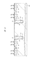
- 主面に形成された複数の第1集積回路素子と、前記主面および裏面を貫通するように形成された複数の第1貫通孔と、前記複数の第1貫通孔のそれぞれの内部に形成され、前記複数の集積回路素子のいずれかに電気的に接続された第1導電膜とを有する第1半導体基板を備えた半導体装置であって、
前記主面における前記複数の第1貫通孔のそれぞれの開口形状は、長方形であり、
前記複数の第1貫通孔は、その長辺が前記主面の第1方向に沿って配向された第1群の貫通孔と、前記長辺が前記主面の第1方向とは異なる第2方向に沿って配向された第2群の貫通孔とを含み、
前記主面における前記第1群の貫通孔の数と前記第2群の貫通孔の数は、等しく、
前記第1群の貫通孔と前記第2群の貫通孔は、電気的に分離されており、
前記第1群の貫通孔の開口形状と前記第2群の貫通孔の開口形状は、等しいことを特徴とする半導体装置。 - 前記主面における前記第1方向と前記第2方向とのなす角は、90度であることを特徴とする請求項1記載の半導体装置。
- 前記主面における前記第1方向と前記第2方向とのなす角は、45度であることを特徴とする請求項1記載の半導体装置。
- 前記複数の第1貫通孔は、それぞれの長辺が同一方向に配向され、かつそれぞれの短辺方向に沿って一列に配列された2個の第1貫通孔を一組とする複数組の貫通孔によって構成されることを特徴とする請求項1記載の半導体装置。
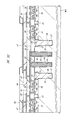
- 主面に複数の第2集積回路素子が形成された第2半導体基板をさらに備え、前記第2半導体基板上に前記第1半導体基板が積層され、前記第1半導体基板の主面に形成された前記第1集積回路素子のいずれかと、前記第2半導体基板の主面に形成された前記第2集積回路素子のいずれかとが、前記複数の第1貫通孔を介して互いに電気的に接続されていることを特徴とする請求項1記載の半導体装置。
- 前記第1半導体基板の厚さと前記第2半導体基板の厚さは異なることを特徴とする請求項5記載の半導体装置。
- 前記第2半導体基板は、その主面および裏面を貫通するように形成された複数の第2貫通孔と、前記複数の第2貫通孔のそれぞれの内部に形成され、前記複数の第2集積回路素子のいずれかに電気的に接続された第2導電膜とをさらに有することを特徴とする請求項5記載の半導体装置。
- 前記第1貫通孔は、短辺の長さが1μm以上であり、深さは短辺の長さの1/2よりも深いことを特徴とする請求項5記載の半導体装置。
- 前記第1導電膜は、タングステンを主成分とする導電膜であることを特徴とする請求項1記載の半導体装置。
Priority Applications (1)
| Application Number | Priority Date | Filing Date | Title |
|---|---|---|---|
| JP2007532208A JP4828537B2 (ja) | 2005-08-26 | 2006-08-25 | 半導体装置 |
Applications Claiming Priority (4)
| Application Number | Priority Date | Filing Date | Title |
|---|---|---|---|
| JP2005245553 | 2005-08-26 | ||
| JP2005245553 | 2005-08-26 | ||
| PCT/JP2006/316770 WO2007023963A1 (ja) | 2005-08-26 | 2006-08-25 | 半導体装置 |
| JP2007532208A JP4828537B2 (ja) | 2005-08-26 | 2006-08-25 | 半導体装置 |
Publications (2)
| Publication Number | Publication Date |
|---|---|
| JPWO2007023963A1 JPWO2007023963A1 (ja) | 2009-03-05 |
| JP4828537B2 true JP4828537B2 (ja) | 2011-11-30 |
Family
ID=37771701
Family Applications (1)
| Application Number | Title | Priority Date | Filing Date |
|---|---|---|---|
| JP2007532208A Expired - Fee Related JP4828537B2 (ja) | 2005-08-26 | 2006-08-25 | 半導体装置 |
Country Status (4)
| Country | Link |
|---|---|
| US (1) | US7948088B2 (ja) |
| JP (1) | JP4828537B2 (ja) |
| TW (1) | TWI407539B (ja) |
| WO (1) | WO2007023963A1 (ja) |
Families Citing this family (10)
| Publication number | Priority date | Publication date | Assignee | Title |
|---|---|---|---|---|
| JP4389227B2 (ja) * | 2006-09-28 | 2009-12-24 | エルピーダメモリ株式会社 | 半導体装置の製造方法 |
| JP2008244187A (ja) * | 2007-03-28 | 2008-10-09 | Elpida Memory Inc | 貫通電極および半導体装置 |
| JP5563186B2 (ja) * | 2007-03-30 | 2014-07-30 | ピーエスフォー ルクスコ エスエイアールエル | 半導体装置及びその製造方法 |
| US8710629B2 (en) | 2009-12-17 | 2014-04-29 | Qualcomm Incorporated | Apparatus and method for controlling semiconductor die warpage |
| CN103378030B (zh) * | 2012-04-18 | 2016-04-20 | 中芯国际集成电路制造(上海)有限公司 | 硅通孔结构 |
| EP2793254B1 (en) * | 2013-04-16 | 2015-10-21 | Ams Ag | Semiconductor device with through-substrate via of enhanced conductivity and corresponding fabrication method |
| JP2016174101A (ja) * | 2015-03-17 | 2016-09-29 | 株式会社東芝 | 半導体装置およびその製造方法 |
| US9543192B2 (en) * | 2015-05-18 | 2017-01-10 | Globalfoundries Singapore Pte. Ltd. | Stitched devices |
| CN106783674B (zh) * | 2016-12-05 | 2019-12-06 | 河北昂扬微电子科技有限公司 | 超薄晶圆翘曲的控制方法 |
| CN113053804B (zh) * | 2021-03-10 | 2023-02-21 | 中国科学院微电子研究所 | 一种钨复合膜层及其生长方法、单片3dic |
Citations (4)
| Publication number | Priority date | Publication date | Assignee | Title |
|---|---|---|---|---|
| JP2002043502A (ja) * | 2000-07-25 | 2002-02-08 | Toshiba Corp | マルチチップ半導体装置、ならびにマルチチップ半導体装置用チップ及びその製造方法 |
| JP2004179673A (ja) * | 2001-05-30 | 2004-06-24 | Sharp Corp | 半導体装置の製造方法 |
| JP2004221430A (ja) * | 2003-01-16 | 2004-08-05 | Nec Electronics Corp | 半導体装置およびそのマスクパターン |
| JP2006165025A (ja) * | 2004-12-02 | 2006-06-22 | Nec Electronics Corp | 半導体装置およびそれを用いた半導体モジュール、ならびに半導体装置の製造方法 |
Family Cites Families (8)
| Publication number | Priority date | Publication date | Assignee | Title |
|---|---|---|---|---|
| JPH11261000A (ja) | 1998-03-13 | 1999-09-24 | Japan Science & Technology Corp | 3次元半導体集積回路装置の製造方法 |
| JP2002124517A (ja) * | 2000-10-13 | 2002-04-26 | Sharp Corp | 半導体装置およびその製造方法 |
| JP2002151796A (ja) * | 2000-11-13 | 2002-05-24 | Sharp Corp | 窒化物半導体発光素子とこれを含む装置 |
| JP2002334967A (ja) | 2001-05-07 | 2002-11-22 | Sony Corp | 3次元半導体チップ |
| US7095114B2 (en) * | 2001-05-30 | 2006-08-22 | Sharp Kabushiki Kaisha | Semiconductor device with via hole group generating high frequency electromagnetic bonding, manufacturing method thereof, and monolithic microwave integrated circuit |
| JP4190211B2 (ja) * | 2002-06-05 | 2008-12-03 | 株式会社東京精密 | 基板加工方法および基板加工装置 |
| JP2005085963A (ja) * | 2003-09-08 | 2005-03-31 | Sharp Corp | 半導体装置およびその製造方法 |
| US7767493B2 (en) * | 2005-06-14 | 2010-08-03 | John Trezza | Post & penetration interconnection |
-
2006
- 2006-08-25 US US12/063,606 patent/US7948088B2/en not_active Expired - Fee Related
- 2006-08-25 WO PCT/JP2006/316770 patent/WO2007023963A1/ja active Application Filing
- 2006-08-25 JP JP2007532208A patent/JP4828537B2/ja not_active Expired - Fee Related
- 2006-08-25 TW TW095131381A patent/TWI407539B/zh not_active IP Right Cessation
Patent Citations (4)
| Publication number | Priority date | Publication date | Assignee | Title |
|---|---|---|---|---|
| JP2002043502A (ja) * | 2000-07-25 | 2002-02-08 | Toshiba Corp | マルチチップ半導体装置、ならびにマルチチップ半導体装置用チップ及びその製造方法 |
| JP2004179673A (ja) * | 2001-05-30 | 2004-06-24 | Sharp Corp | 半導体装置の製造方法 |
| JP2004221430A (ja) * | 2003-01-16 | 2004-08-05 | Nec Electronics Corp | 半導体装置およびそのマスクパターン |
| JP2006165025A (ja) * | 2004-12-02 | 2006-06-22 | Nec Electronics Corp | 半導体装置およびそれを用いた半導体モジュール、ならびに半導体装置の製造方法 |
Also Published As
| Publication number | Publication date |
|---|---|
| US20090174080A1 (en) | 2009-07-09 |
| TWI407539B (zh) | 2013-09-01 |
| WO2007023963A1 (ja) | 2007-03-01 |
| JPWO2007023963A1 (ja) | 2009-03-05 |
| TW200725865A (en) | 2007-07-01 |
| US7948088B2 (en) | 2011-05-24 |
Similar Documents
| Publication | Publication Date | Title |
|---|---|---|
| JP4916444B2 (ja) | 半導体装置の製造方法 | |
| JP4828537B2 (ja) | 半導体装置 | |
| US8354730B2 (en) | Manufacturing method of semiconductor device and semiconductor device | |
| US7812457B2 (en) | Semiconductor device and semiconductor wafer and a method for manufacturing the same | |
| JP2008091852A (ja) | 積層パッケージおよびその製造方法 | |
| CN102468247B (zh) | 附着聚酰亚胺层的密封环结构 | |
| US10424508B2 (en) | Interconnection structure having a via structure and fabrication thereof | |
| US7535062B2 (en) | Semiconductor device having SOI structure | |
| JP2009152583A (ja) | 半導体素子及びその製造方法 | |
| JP2009055004A (ja) | 貫通配線構造 | |
| US11521937B2 (en) | Package structures with built-in EMI shielding | |
| WO2010035375A1 (ja) | 半導体装置及びその製造方法 | |
| JP2011071441A (ja) | 半導体装置の製造方法、半導体装置およびウエハ積層構造物 | |
| TW202034403A (zh) | 半導體裝置及其製造方法 | |
| JP4945545B2 (ja) | 半導体装置の製造方法 | |
| JP2015099827A (ja) | 半導体装置および半導体装置の製造方法 | |
| JP5271562B2 (ja) | 半導体装置および半導体装置の製造方法 | |
| JP2018088487A (ja) | 半導体装置及びその製造方法 | |
| WO2010082248A1 (ja) | 半導体装置およびそれを用いた電子機器ならびに半導体装置の製造方法 | |
| CN104347529A (zh) | 半导体装置及其制造方法、以及半导体装置的安装方法 | |
| JP4696152B2 (ja) | 半導体装置の製造方法および半導体装置 | |
| WO2011148444A1 (ja) | 半導体装置及びその製造方法 |
Legal Events
| Date | Code | Title | Description |
|---|---|---|---|
| A131 | Notification of reasons for refusal |
Free format text: JAPANESE INTERMEDIATE CODE: A131 Effective date: 20100921 |
|
| A521 | Request for written amendment filed |
Free format text: JAPANESE INTERMEDIATE CODE: A523 Effective date: 20101119 |
|
| TRDD | Decision of grant or rejection written | ||
| A01 | Written decision to grant a patent or to grant a registration (utility model) |
Free format text: JAPANESE INTERMEDIATE CODE: A01 Effective date: 20110823 |
|
| A01 | Written decision to grant a patent or to grant a registration (utility model) |
Free format text: JAPANESE INTERMEDIATE CODE: A01 |
|
| A61 | First payment of annual fees (during grant procedure) |
Free format text: JAPANESE INTERMEDIATE CODE: A61 Effective date: 20110914 |
|
| FPAY | Renewal fee payment (event date is renewal date of database) |
Free format text: PAYMENT UNTIL: 20140922 Year of fee payment: 3 |
|
| R150 | Certificate of patent or registration of utility model |
Free format text: JAPANESE INTERMEDIATE CODE: R150 |
|
| LAPS | Cancellation because of no payment of annual fees |