JP4752307B2 - 非接触型データキャリア用導電部材とその製造方法及び装置 - Google Patents
非接触型データキャリア用導電部材とその製造方法及び装置 Download PDFInfo
- Publication number
- JP4752307B2 JP4752307B2 JP2005106822A JP2005106822A JP4752307B2 JP 4752307 B2 JP4752307 B2 JP 4752307B2 JP 2005106822 A JP2005106822 A JP 2005106822A JP 2005106822 A JP2005106822 A JP 2005106822A JP 4752307 B2 JP4752307 B2 JP 4752307B2
- Authority
- JP
- Japan
- Prior art keywords
- punching
- conductive layer
- data carrier
- substrate
- conductive
- Prior art date
- Legal status (The legal status is an assumption and is not a legal conclusion. Google has not performed a legal analysis and makes no representation as to the accuracy of the status listed.)
- Expired - Fee Related
Links
Images


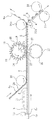


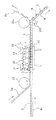


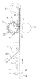

Classifications
-
- H—ELECTRICITY
- H05—ELECTRIC TECHNIQUES NOT OTHERWISE PROVIDED FOR
- H05K—PRINTED CIRCUITS; CASINGS OR CONSTRUCTIONAL DETAILS OF ELECTRIC APPARATUS; MANUFACTURE OF ASSEMBLAGES OF ELECTRICAL COMPONENTS
- H05K3/00—Apparatus or processes for manufacturing printed circuits
- H05K3/02—Apparatus or processes for manufacturing printed circuits in which the conductive material is applied to the surface of the insulating support and is thereafter removed from such areas of the surface which are not intended for current conducting or shielding
- H05K3/04—Apparatus or processes for manufacturing printed circuits in which the conductive material is applied to the surface of the insulating support and is thereafter removed from such areas of the surface which are not intended for current conducting or shielding the conductive material being removed mechanically, e.g. by punching
- H05K3/046—Apparatus or processes for manufacturing printed circuits in which the conductive material is applied to the surface of the insulating support and is thereafter removed from such areas of the surface which are not intended for current conducting or shielding the conductive material being removed mechanically, e.g. by punching by selective transfer or selective detachment of a conductive layer
-
- H—ELECTRICITY
- H05—ELECTRIC TECHNIQUES NOT OTHERWISE PROVIDED FOR
- H05K—PRINTED CIRCUITS; CASINGS OR CONSTRUCTIONAL DETAILS OF ELECTRIC APPARATUS; MANUFACTURE OF ASSEMBLAGES OF ELECTRICAL COMPONENTS
- H05K2201/00—Indexing scheme relating to printed circuits covered by H05K1/00
- H05K2201/03—Conductive materials
- H05K2201/0332—Structure of the conductor
- H05K2201/0335—Layered conductors or foils
- H05K2201/0355—Metal foils
-
- H—ELECTRICITY
- H05—ELECTRIC TECHNIQUES NOT OTHERWISE PROVIDED FOR
- H05K—PRINTED CIRCUITS; CASINGS OR CONSTRUCTIONAL DETAILS OF ELECTRIC APPARATUS; MANUFACTURE OF ASSEMBLAGES OF ELECTRICAL COMPONENTS
- H05K2203/00—Indexing scheme relating to apparatus or processes for manufacturing printed circuits covered by H05K3/00
- H05K2203/05—Patterning and lithography; Masks; Details of resist
- H05K2203/0502—Patterning and lithography
- H05K2203/0522—Using an adhesive pattern
-
- H—ELECTRICITY
- H05—ELECTRIC TECHNIQUES NOT OTHERWISE PROVIDED FOR
- H05K—PRINTED CIRCUITS; CASINGS OR CONSTRUCTIONAL DETAILS OF ELECTRIC APPARATUS; MANUFACTURE OF ASSEMBLAGES OF ELECTRICAL COMPONENTS
- H05K2203/00—Indexing scheme relating to apparatus or processes for manufacturing printed circuits covered by H05K3/00
- H05K2203/15—Position of the PCB during processing
- H05K2203/1545—Continuous processing, i.e. involving rolls moving a band-like or solid carrier along a continuous production path
-
- H—ELECTRICITY
- H05—ELECTRIC TECHNIQUES NOT OTHERWISE PROVIDED FOR
- H05K—PRINTED CIRCUITS; CASINGS OR CONSTRUCTIONAL DETAILS OF ELECTRIC APPARATUS; MANUFACTURE OF ASSEMBLAGES OF ELECTRICAL COMPONENTS
- H05K3/00—Apparatus or processes for manufacturing printed circuits
- H05K3/02—Apparatus or processes for manufacturing printed circuits in which the conductive material is applied to the surface of the insulating support and is thereafter removed from such areas of the surface which are not intended for current conducting or shielding
- H05K3/04—Apparatus or processes for manufacturing printed circuits in which the conductive material is applied to the surface of the insulating support and is thereafter removed from such areas of the surface which are not intended for current conducting or shielding the conductive material being removed mechanically, e.g. by punching
- H05K3/041—Apparatus or processes for manufacturing printed circuits in which the conductive material is applied to the surface of the insulating support and is thereafter removed from such areas of the surface which are not intended for current conducting or shielding the conductive material being removed mechanically, e.g. by punching by using a die for cutting the conductive material
-
- Y—GENERAL TAGGING OF NEW TECHNOLOGICAL DEVELOPMENTS; GENERAL TAGGING OF CROSS-SECTIONAL TECHNOLOGIES SPANNING OVER SEVERAL SECTIONS OF THE IPC; TECHNICAL SUBJECTS COVERED BY FORMER USPC CROSS-REFERENCE ART COLLECTIONS [XRACs] AND DIGESTS
- Y10—TECHNICAL SUBJECTS COVERED BY FORMER USPC
- Y10T—TECHNICAL SUBJECTS COVERED BY FORMER US CLASSIFICATION
- Y10T156/00—Adhesive bonding and miscellaneous chemical manufacture
- Y10T156/10—Methods of surface bonding and/or assembly therefor
- Y10T156/1052—Methods of surface bonding and/or assembly therefor with cutting, punching, tearing or severing
- Y10T156/1054—Methods of surface bonding and/or assembly therefor with cutting, punching, tearing or severing and simultaneously bonding [e.g., cut-seaming]
-
- Y—GENERAL TAGGING OF NEW TECHNOLOGICAL DEVELOPMENTS; GENERAL TAGGING OF CROSS-SECTIONAL TECHNOLOGIES SPANNING OVER SEVERAL SECTIONS OF THE IPC; TECHNICAL SUBJECTS COVERED BY FORMER USPC CROSS-REFERENCE ART COLLECTIONS [XRACs] AND DIGESTS
- Y10—TECHNICAL SUBJECTS COVERED BY FORMER USPC
- Y10T—TECHNICAL SUBJECTS COVERED BY FORMER US CLASSIFICATION
- Y10T29/00—Metal working
- Y10T29/49—Method of mechanical manufacture
- Y10T29/49002—Electrical device making
- Y10T29/49117—Conductor or circuit manufacturing
- Y10T29/49124—On flat or curved insulated base, e.g., printed circuit, etc.
- Y10T29/49126—Assembling bases
-
- Y—GENERAL TAGGING OF NEW TECHNOLOGICAL DEVELOPMENTS; GENERAL TAGGING OF CROSS-SECTIONAL TECHNOLOGIES SPANNING OVER SEVERAL SECTIONS OF THE IPC; TECHNICAL SUBJECTS COVERED BY FORMER USPC CROSS-REFERENCE ART COLLECTIONS [XRACs] AND DIGESTS
- Y10—TECHNICAL SUBJECTS COVERED BY FORMER USPC
- Y10T—TECHNICAL SUBJECTS COVERED BY FORMER US CLASSIFICATION
- Y10T29/00—Metal working
- Y10T29/49—Method of mechanical manufacture
- Y10T29/49002—Electrical device making
- Y10T29/49117—Conductor or circuit manufacturing
- Y10T29/49124—On flat or curved insulated base, e.g., printed circuit, etc.
- Y10T29/49128—Assembling formed circuit to base
-
- Y—GENERAL TAGGING OF NEW TECHNOLOGICAL DEVELOPMENTS; GENERAL TAGGING OF CROSS-SECTIONAL TECHNOLOGIES SPANNING OVER SEVERAL SECTIONS OF THE IPC; TECHNICAL SUBJECTS COVERED BY FORMER USPC CROSS-REFERENCE ART COLLECTIONS [XRACs] AND DIGESTS
- Y10—TECHNICAL SUBJECTS COVERED BY FORMER USPC
- Y10T—TECHNICAL SUBJECTS COVERED BY FORMER US CLASSIFICATION
- Y10T29/00—Metal working
- Y10T29/49—Method of mechanical manufacture
- Y10T29/49002—Electrical device making
- Y10T29/49117—Conductor or circuit manufacturing
- Y10T29/49124—On flat or curved insulated base, e.g., printed circuit, etc.
- Y10T29/49155—Manufacturing circuit on or in base
- Y10T29/49156—Manufacturing circuit on or in base with selective destruction of conductive paths
-
- Y—GENERAL TAGGING OF NEW TECHNOLOGICAL DEVELOPMENTS; GENERAL TAGGING OF CROSS-SECTIONAL TECHNOLOGIES SPANNING OVER SEVERAL SECTIONS OF THE IPC; TECHNICAL SUBJECTS COVERED BY FORMER USPC CROSS-REFERENCE ART COLLECTIONS [XRACs] AND DIGESTS
- Y10—TECHNICAL SUBJECTS COVERED BY FORMER USPC
- Y10T—TECHNICAL SUBJECTS COVERED BY FORMER US CLASSIFICATION
- Y10T29/00—Metal working
- Y10T29/49—Method of mechanical manufacture
- Y10T29/49002—Electrical device making
- Y10T29/49117—Conductor or circuit manufacturing
- Y10T29/49124—On flat or curved insulated base, e.g., printed circuit, etc.
- Y10T29/49155—Manufacturing circuit on or in base
- Y10T29/49163—Manufacturing circuit on or in base with sintering of base
Landscapes
- Engineering & Computer Science (AREA)
- Manufacturing & Machinery (AREA)
- Microelectronics & Electronic Packaging (AREA)
- Details Of Aerials (AREA)
- Credit Cards Or The Like (AREA)
Priority Applications (6)
| Application Number | Priority Date | Filing Date | Title |
|---|---|---|---|
| JP2005106822A JP4752307B2 (ja) | 2004-04-28 | 2005-04-01 | 非接触型データキャリア用導電部材とその製造方法及び装置 |
| US11/578,311 US7930822B2 (en) | 2004-04-28 | 2005-04-20 | Method and device for manufacturing a conductive member for non-contact type data carrier |
| PCT/JP2005/007527 WO2005107347A1 (ja) | 2004-04-28 | 2005-04-20 | 非接触型データキャリア用導電部材とその製造方法及び装置 |
| EP05734388A EP1744607A4 (en) | 2004-04-28 | 2005-04-20 | CONDUCTIVE MEMBER FOR NON-CONTACT DATA CARRIER AND METHOD AND DEVICE FOR MANUFACTURING THE SAME |
| CN2005800186423A CN1985552B (zh) | 2004-04-28 | 2005-04-20 | 用于非接触型数据载体的导电元件及其制造方法和装置 |
| TW094113409A TW200540026A (en) | 2004-04-28 | 2005-04-27 | Conductive member for non-contact data carrier and manufacturing method and device thereof |
Applications Claiming Priority (5)
| Application Number | Priority Date | Filing Date | Title |
|---|---|---|---|
| JP2004134659 | 2004-04-28 | ||
| JP2004134659 | 2004-04-28 | ||
| JP2005058239 | 2005-03-02 | ||
| JP2005058239 | 2005-03-02 | ||
| JP2005106822A JP4752307B2 (ja) | 2004-04-28 | 2005-04-01 | 非接触型データキャリア用導電部材とその製造方法及び装置 |
Publications (2)
| Publication Number | Publication Date |
|---|---|
| JP2006277700A JP2006277700A (ja) | 2006-10-12 |
| JP4752307B2 true JP4752307B2 (ja) | 2011-08-17 |
Family
ID=35242084
Family Applications (1)
| Application Number | Title | Priority Date | Filing Date |
|---|---|---|---|
| JP2005106822A Expired - Fee Related JP4752307B2 (ja) | 2004-04-28 | 2005-04-01 | 非接触型データキャリア用導電部材とその製造方法及び装置 |
Country Status (6)
| Country | Link |
|---|---|
| US (1) | US7930822B2 (enExample) |
| EP (1) | EP1744607A4 (enExample) |
| JP (1) | JP4752307B2 (enExample) |
| CN (1) | CN1985552B (enExample) |
| TW (1) | TW200540026A (enExample) |
| WO (1) | WO2005107347A1 (enExample) |
Families Citing this family (22)
| Publication number | Priority date | Publication date | Assignee | Title |
|---|---|---|---|---|
| JP4779556B2 (ja) * | 2005-10-07 | 2011-09-28 | 大日本印刷株式会社 | 非接触型データキャリア用導電部材の製造方法及び装置 |
| JP2008015969A (ja) * | 2006-07-10 | 2008-01-24 | Dainippon Printing Co Ltd | 非接触型データキャリア用導電部材の製造方法及び装置 |
| US8162231B2 (en) | 2006-11-01 | 2012-04-24 | Dai Nippon Printing Co., Ltd. | Noncontact IC tag label and method of manufacturing the same |
| JP5083091B2 (ja) * | 2008-07-24 | 2012-11-28 | 大日本印刷株式会社 | 非接触型データキャリア用導電部材の形成方法及び装置 |
| JP5128676B2 (ja) * | 2008-11-14 | 2013-01-23 | 凸版印刷株式会社 | 非接触icラベルおよび物品 |
| WO2012067225A1 (ja) * | 2010-11-19 | 2012-05-24 | 凸版印刷株式会社 | 金属箔パターン積層体、金属箔の型抜き方法、回路基板、その製造方法、および太陽電池モジュール |
| KR102067846B1 (ko) * | 2011-06-06 | 2020-01-17 | 디에스엠 아이피 어셋츠 비.브이. | 금속박 패턴 적층체, 금속박 적층체, 금속박 적층 기판, 태양 전지 모듈 및 금속박 패턴 적층체의 제조 방법 |
| WO2013019922A2 (en) | 2011-08-03 | 2013-02-07 | Graphic Packaging International, Inc. | Systems and methods for forming laminates with patterned microwave energy interactive material |
| DE102012209328A1 (de) * | 2012-06-01 | 2013-12-05 | 3D-Micromac Ag | Verfahren und Anlage zum Herstellen eines Mehrschichtelements sowie Mehrschichtelement |
| US9380709B2 (en) | 2013-03-15 | 2016-06-28 | Taiwan Semiconductor Manufacturing Co., Ltd. | Method of cutting conductive patterns |
| WO2015048000A1 (en) * | 2013-09-26 | 2015-04-02 | Graphic Packaging International, Inc. | Laminates, and systems and methods for laminating |
| JP6379667B2 (ja) * | 2014-05-21 | 2018-08-29 | Tdk株式会社 | アンテナ装置及びその製造方法 |
| WO2016070915A1 (de) * | 2014-11-05 | 2016-05-12 | Ev Group E. Thallner Gmbh | Verfahren und vorrichtung zum beschichten eines produktsubstrats |
| ES2873874T3 (es) | 2014-12-22 | 2021-11-04 | Graphic Packaging Int Llc | Sistemas y procedimientos para formar laminados |
| EP3432224B1 (en) * | 2016-03-18 | 2022-06-29 | Sato Holdings Kabushiki Kaisha | Method for manufacturing an rfid inlet |
| CN107482302A (zh) * | 2017-07-01 | 2017-12-15 | 华中科技大学 | 一种rfid天线制作方法 |
| CN108566732B (zh) * | 2018-05-14 | 2020-09-01 | 龙南骏亚柔性智能科技有限公司 | 一种柔性pcb电子器件褶皱制备结构 |
| WO2020141331A1 (en) * | 2019-01-04 | 2020-07-09 | Sherkin Technologies Uk Ltd | Improvements in or relating to flexible electronics |
| US10709022B1 (en) * | 2019-04-19 | 2020-07-07 | Gentherm Incorporated | Milling of flex foil with two conductive layers from both sides |
| CN112589913A (zh) * | 2021-03-05 | 2021-04-02 | 赛柯赛斯新能源科技(苏州)有限公司 | 柔性电路板圆刀裁切工艺及其加工装置 |
| CN117048173A (zh) * | 2023-08-28 | 2023-11-14 | 晶科能源股份有限公司 | 层压机及层压机的层压方法 |
| CN118514411A (zh) * | 2024-04-19 | 2024-08-20 | 隆基绿能科技股份有限公司 | 一种光伏背板加工设备及方法 |
Family Cites Families (16)
| Publication number | Priority date | Publication date | Assignee | Title |
|---|---|---|---|---|
| US3573126A (en) * | 1968-06-07 | 1971-03-30 | Gti Corp | Methods of manufacturing electrical circuits |
| US3713944A (en) * | 1970-05-28 | 1973-01-30 | Essex International Inc | A method of manufacture of printed circuits by die stamping |
| US4091125A (en) * | 1976-11-08 | 1978-05-23 | Delgadillo Joseph A | Circuit board and method for producing same |
| US4682415A (en) * | 1985-10-28 | 1987-07-28 | U.S. Product Development Company | Method of making printed circuits |
| ATE440480T1 (de) * | 1993-12-30 | 2009-09-15 | Miyake Kk | Verbundfolie mit schaltungsfírmiger metallfolie oder dergleichen und verfahren zur herstellung |
| JP3116209B2 (ja) | 1994-12-01 | 2000-12-11 | 株式会社三宅 | 共振タグ等の回路様金属箔シートの製造方法 |
| US5759422A (en) * | 1996-02-14 | 1998-06-02 | Fort James Corporation | Patterned metal foil laminate and method for making same |
| JPH10187922A (ja) * | 1996-10-23 | 1998-07-21 | Furukawa Electric Co Ltd:The | プリペイドカード |
| US6320556B1 (en) * | 2000-01-19 | 2001-11-20 | Moore North America, Inc. | RFID foil or film antennas |
| JP3536977B2 (ja) * | 2000-10-24 | 2004-06-14 | ローム株式会社 | 非接触型icカード及びその集合体及びその製造方法 |
| JP2002298109A (ja) * | 2001-03-30 | 2002-10-11 | Toppan Forms Co Ltd | 非接触型icメディアおよびその製造方法 |
| JP4770065B2 (ja) * | 2001-06-06 | 2011-09-07 | 大日本印刷株式会社 | 意匠性の高いrfidタグ、およびその製造方法 |
| DE10145749A1 (de) * | 2001-09-17 | 2003-04-24 | Infineon Technologies Ag | Verfahren zur Herstellung einer strukturierten Metallschicht auf einem Trägerkörper und Trägerkörper mit einer strukturierten Metallschicht |
| JP3998975B2 (ja) * | 2001-12-28 | 2007-10-31 | 大日本印刷株式会社 | 電磁波遮蔽用シート |
| FR2841089B1 (fr) * | 2002-06-14 | 2004-07-30 | Sequoias | Procede de fabrication industrielle, en ligne, d'antennes pour transpondeurs rfid |
| JP4012019B2 (ja) * | 2002-08-30 | 2007-11-21 | 大日本印刷株式会社 | アンテナ配線パターンの形成方法 |
-
2005
- 2005-04-01 JP JP2005106822A patent/JP4752307B2/ja not_active Expired - Fee Related
- 2005-04-20 US US11/578,311 patent/US7930822B2/en active Active
- 2005-04-20 EP EP05734388A patent/EP1744607A4/en not_active Withdrawn
- 2005-04-20 CN CN2005800186423A patent/CN1985552B/zh not_active Expired - Fee Related
- 2005-04-20 WO PCT/JP2005/007527 patent/WO2005107347A1/ja not_active Ceased
- 2005-04-27 TW TW094113409A patent/TW200540026A/zh not_active IP Right Cessation
Also Published As
| Publication number | Publication date |
|---|---|
| TWI351354B (enExample) | 2011-11-01 |
| CN1985552B (zh) | 2012-09-05 |
| EP1744607A4 (en) | 2010-10-27 |
| EP1744607A1 (en) | 2007-01-17 |
| TW200540026A (en) | 2005-12-16 |
| CN1985552A (zh) | 2007-06-20 |
| US20070214637A1 (en) | 2007-09-20 |
| US7930822B2 (en) | 2011-04-26 |
| JP2006277700A (ja) | 2006-10-12 |
| WO2005107347A1 (ja) | 2005-11-10 |
Similar Documents
| Publication | Publication Date | Title |
|---|---|---|
| TWI351354B (enExample) | ||
| JP7105333B2 (ja) | アンテナパターンの製造方法、rfidインレットの製造方法、rfidラベルの製造方法及びrfid媒体の製造方法 | |
| US11710886B2 (en) | Foil laminate intermediate and method of manufacturing | |
| JP7353985B2 (ja) | 回路パターン、rfidインレイ、rfidラベル及びrfid媒体 | |
| US20080295318A1 (en) | Method and Device for Continuously Producing Electronic Film Components and an Electronic Film Component | |
| JP7722822B2 (ja) | Rfidラベルの製造方法 | |
| JP2005339518A (ja) | 非接触型データキャリア用導電部材とその製造方法及び装置 | |
| JP2005340773A (ja) | 非接触型データキャリア用導電部材とその製造方法及び装置 | |
| KR100739374B1 (ko) | Rfid 태그 | |
| JP4779556B2 (ja) | 非接触型データキャリア用導電部材の製造方法及び装置 | |
| JP2005311179A (ja) | 非接触データキャリア用導電部材製造方法および非接触データキャリア用導電部材製造装置 | |
| JP5083091B2 (ja) | 非接触型データキャリア用導電部材の形成方法及び装置 | |
| JP2005339509A (ja) | 非接触型データキャリア用導電部材とその製造方法及び装置 | |
| JP4012019B2 (ja) | アンテナ配線パターンの形成方法 | |
| JP2005346696A (ja) | 非接触型データキャリア用導電部材とその製造方法及び装置 | |
| JP2005339517A (ja) | 非接触型データキャリア用導電部材とその製造方法及び装置 | |
| WO2023047949A1 (ja) | Rfid容器及びrfid容器の製造方法 | |
| JP2009031964A (ja) | 非接触icタグの製造方法及び装置 | |
| JP5167619B2 (ja) | 非接触型データキャリア用導電シートの製造方法及び装置、icタグ付きシートの製造装置。 | |
| JP2005346695A (ja) | 非接触型データキャリア用導電部材とその製造方法及び装置 | |
| JP5050426B2 (ja) | 非接触icタグの製造方法及び装置 | |
| JP7587949B2 (ja) | アンテナパターンの製造方法 | |
| JP4910344B2 (ja) | 非接触型icタグとその製造方法 | |
| JP4629535B2 (ja) | 非接触データキャリア用部材の製造方法及び成形型 | |
| JP5018370B2 (ja) | 非接触型データキャリア用導電部材とその製造方法及び装置 |
Legal Events
| Date | Code | Title | Description |
|---|---|---|---|
| A621 | Written request for application examination |
Free format text: JAPANESE INTERMEDIATE CODE: A621 Effective date: 20080312 |
|
| A131 | Notification of reasons for refusal |
Free format text: JAPANESE INTERMEDIATE CODE: A131 Effective date: 20110208 |
|
| RD02 | Notification of acceptance of power of attorney |
Free format text: JAPANESE INTERMEDIATE CODE: A7422 Effective date: 20110216 |
|
| A521 | Written amendment |
Free format text: JAPANESE INTERMEDIATE CODE: A523 Effective date: 20110408 |
|
| TRDD | Decision of grant or rejection written | ||
| A01 | Written decision to grant a patent or to grant a registration (utility model) |
Free format text: JAPANESE INTERMEDIATE CODE: A01 Effective date: 20110426 |
|
| A61 | First payment of annual fees (during grant procedure) |
Free format text: JAPANESE INTERMEDIATE CODE: A61 Effective date: 20110509 |
|
| FPAY | Renewal fee payment (event date is renewal date of database) |
Free format text: PAYMENT UNTIL: 20140603 Year of fee payment: 3 |
|
| R150 | Certificate of patent or registration of utility model |
Ref document number: 4752307 Country of ref document: JP Free format text: JAPANESE INTERMEDIATE CODE: R150 Free format text: JAPANESE INTERMEDIATE CODE: R150 |
|
| LAPS | Cancellation because of no payment of annual fees |