JP4668729B2 - 半導体装置の製造方法 - Google Patents
半導体装置の製造方法 Download PDFInfo
- Publication number
- JP4668729B2 JP4668729B2 JP2005236591A JP2005236591A JP4668729B2 JP 4668729 B2 JP4668729 B2 JP 4668729B2 JP 2005236591 A JP2005236591 A JP 2005236591A JP 2005236591 A JP2005236591 A JP 2005236591A JP 4668729 B2 JP4668729 B2 JP 4668729B2
- Authority
- JP
- Japan
- Prior art keywords
- tab
- semiconductor chip
- frame
- resin
- die attach
- Prior art date
- Legal status (The legal status is an assumption and is not a legal conclusion. Google has not performed a legal analysis and makes no representation as to the accuracy of the status listed.)
- Expired - Fee Related
Links
Images


Classifications
-
- H—ELECTRICITY
- H01—ELECTRIC ELEMENTS
- H01L—SEMICONDUCTOR DEVICES NOT COVERED BY CLASS H10
- H01L2224/00—Indexing scheme for arrangements for connecting or disconnecting semiconductor or solid-state bodies and methods related thereto as covered by H01L24/00
- H01L2224/01—Means for bonding being attached to, or being formed on, the surface to be connected, e.g. chip-to-package, die-attach, "first-level" interconnects; Manufacturing methods related thereto
- H01L2224/42—Wire connectors; Manufacturing methods related thereto
- H01L2224/44—Structure, shape, material or disposition of the wire connectors prior to the connecting process
- H01L2224/45—Structure, shape, material or disposition of the wire connectors prior to the connecting process of an individual wire connector
- H01L2224/45001—Core members of the connector
- H01L2224/45099—Material
- H01L2224/451—Material with a principal constituent of the material being a metal or a metalloid, e.g. boron (B), silicon (Si), germanium (Ge), arsenic (As), antimony (Sb), tellurium (Te) and polonium (Po), and alloys thereof
- H01L2224/45138—Material with a principal constituent of the material being a metal or a metalloid, e.g. boron (B), silicon (Si), germanium (Ge), arsenic (As), antimony (Sb), tellurium (Te) and polonium (Po), and alloys thereof the principal constituent melting at a temperature of greater than or equal to 950°C and less than 1550°C
- H01L2224/45144—Gold (Au) as principal constituent
-
- H—ELECTRICITY
- H01—ELECTRIC ELEMENTS
- H01L—SEMICONDUCTOR DEVICES NOT COVERED BY CLASS H10
- H01L2224/00—Indexing scheme for arrangements for connecting or disconnecting semiconductor or solid-state bodies and methods related thereto as covered by H01L24/00
- H01L2224/01—Means for bonding being attached to, or being formed on, the surface to be connected, e.g. chip-to-package, die-attach, "first-level" interconnects; Manufacturing methods related thereto
- H01L2224/42—Wire connectors; Manufacturing methods related thereto
- H01L2224/47—Structure, shape, material or disposition of the wire connectors after the connecting process
- H01L2224/48—Structure, shape, material or disposition of the wire connectors after the connecting process of an individual wire connector
- H01L2224/481—Disposition
- H01L2224/48151—Connecting between a semiconductor or solid-state body and an item not being a semiconductor or solid-state body, e.g. chip-to-substrate, chip-to-passive
- H01L2224/48221—Connecting between a semiconductor or solid-state body and an item not being a semiconductor or solid-state body, e.g. chip-to-substrate, chip-to-passive the body and the item being stacked
- H01L2224/48245—Connecting between a semiconductor or solid-state body and an item not being a semiconductor or solid-state body, e.g. chip-to-substrate, chip-to-passive the body and the item being stacked the item being metallic
- H01L2224/48247—Connecting between a semiconductor or solid-state body and an item not being a semiconductor or solid-state body, e.g. chip-to-substrate, chip-to-passive the body and the item being stacked the item being metallic connecting the wire to a bond pad of the item
Description
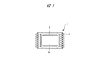
図1は、本実施の形態1における半導体装置1の一部を示した図である。図1において、本実施の形態1における半導体装置1のパッケージ形態は、TSOP(パッケージの取り付け面からの高さが1.2mm以下)である。このTSOPでは、半導体チップの搭載にタブを用いる。半導体装置1の中央部には、内部がくりぬかれて枠形状をした枠タブ2が形成されている。すなわち、半導体装置1の中央部には、内部に空洞部2aが形成されている枠タブ2が形成されている。この枠タブ2は、半導体チップを搭載するものであり、長方形状の枠形状をしている。そして、枠タブ2の周囲には、複数のリード3が形成されている。
上には、半導体チップ4が搭載されている。半導体チップ4の裏面全面には、粘着性のダイアタッチフィルム6が貼り付けられており、このダイアタッチフィルム6によって、枠タブ2と半導体チップ4が接着されている。半導体チップ4の表面には複数のボンディングパッド7が形成されており、このボンディングパッド7とリード3とは、ワイヤ5で電気的に接続されている。そして、半導体チップ4からリードの一部にわたって樹脂で封止され、TSOPによるパッケージが形成されている。
前記実施の形態1では、半導体チップの外縁部にボンディングパッドがある例について説明したが、本実施の形態2では、半導体チップの中央部にボンディングパッドがある例について説明する。
前記実施の形態1のパッケージ形態はTSOPであったが、本実施の形態3は、パッケージ形態がQFPである場合について説明する。
2 枠タブ
2a 空洞部
3 リード
4 半導体チップ
5 ワイヤ
6 ダイアタッチフィルム
7 ボンディングパッド
8 樹脂
9 溝
10 半導体ウェハ
10a 半導体チップ
11 治具
12 ダイシングテープ
13 ダイアタッチフィルム
14 吸着ステージ
15 ブレード
16 突き上げ駒
17 コレット
18 ヒータステージ
19 リード
20 枠タブ
20a 空洞部
21 ボンディングパッド
22 ワイヤ
23 溝
24 気泡
25 樹脂
26 アウターリード
27 実装基板
28 端子
29 半田
30 半導体装置
31 枠タブ
32 タブ材
33 リード
34 半導体チップ
35 ボンディングパッド
36 ワイヤ
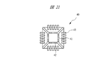
40 半導体装置
41 枠タブ
42 溝
43 リード
44 半導体チップ
45 ワイヤ
100 半導体チップ
101 タブ
102 樹脂
103 ダイアタッチフィルム
105 ヒータステージ
106 タブ
Claims (3)
- 以下の工程を含むことを特徴とする半導体装置の製造方法:
(a)上面、前記上面とは反対側の下面を有するタブと、平面視において前記タブの周囲に配置された複数のリードとを備えたリードフレームを準備する工程;
(b)前記(a)工程の後、表面、前記表面に形成された複数のボンディングパッド、前記表面とは反対側の裏面を有する半導体チップを、前記半導体チップの前記裏面が前記タブの前記上面と対向するように、ダイアタッチフィルムを介して前記タブの前記上面に搭載する工程;
(c)前記(b)工程の後、前記半導体チップの前記複数のボンディングパッドと前記複数のリードとを、複数のワイヤを介してそれぞれ電気的に接続する工程;
(d)前記(c)工程の後、前記半導体チップ、前記複数のワイヤ、前記複数のリードのそれぞれの一部、および前記タブを樹脂で封止する工程;
ここで、
前記タブの平面形状は、枠状からなり、
前記タブの前記上面には、ハーフエッチング加工によって溝が形成されており、
前記(b)工程では、平面視において前記半導体チップが前記溝と重なり、かつ、前記ダイアタッチフィルムが前記タブの前記溝内の底面と接触しないように、前記ダイアタッチフィルムを介して前記タブの前記上面に前記半導体チップを固定する。 - 前記タブの平面形状は、互いに対向する一対の第1辺と、前記第1辺とそれぞれ交差し、かつ、互いに対向する一対の第2辺とを有する四角形からなり、
前記複数のリードは、前記第1辺のみに沿って配置されており、
前記溝は、前記タブの前記上面における前記一対の第2辺のみに形成されており、
前記(d)工程では、前記一対の第2辺のうちの一方から他方に向かって前記樹脂を供給することを特徴とする請求項1記載の半導体装置の製造方法。 - 前記(b)工程では、前記複数のボンディングパッドの直下に前記タブが位置するように、前記半導体チップを前記タブに搭載し、
前記(c)工程では、前記タブの前記下面を、発熱したヒータステージに接触させていることを特徴とする請求項1記載の半導体装置の製造方法。
Priority Applications (1)
| Application Number | Priority Date | Filing Date | Title |
|---|---|---|---|
| JP2005236591A JP4668729B2 (ja) | 2005-08-17 | 2005-08-17 | 半導体装置の製造方法 |
Applications Claiming Priority (1)
| Application Number | Priority Date | Filing Date | Title |
|---|---|---|---|
| JP2005236591A JP4668729B2 (ja) | 2005-08-17 | 2005-08-17 | 半導体装置の製造方法 |
Publications (3)
| Publication Number | Publication Date |
|---|---|
| JP2007053195A JP2007053195A (ja) | 2007-03-01 |
| JP2007053195A5 JP2007053195A5 (ja) | 2008-10-02 |
| JP4668729B2 true JP4668729B2 (ja) | 2011-04-13 |
Family
ID=37917443
Family Applications (1)
| Application Number | Title | Priority Date | Filing Date |
|---|---|---|---|
| JP2005236591A Expired - Fee Related JP4668729B2 (ja) | 2005-08-17 | 2005-08-17 | 半導体装置の製造方法 |
Country Status (1)
| Country | Link |
|---|---|
| JP (1) | JP4668729B2 (ja) |
Citations (11)
| Publication number | Priority date | Publication date | Assignee | Title |
|---|---|---|---|---|
| JPS6215844A (ja) * | 1985-07-15 | 1987-01-24 | Hitachi Ltd | 半導体リ−ドフレ−ム |
| JPS63248155A (ja) * | 1987-04-03 | 1988-10-14 | Mitsubishi Electric Corp | 半導体装置 |
| JPH0697354A (ja) * | 1992-07-27 | 1994-04-08 | Motorola Inc | 開口部のあるフラッグを有する半導体装置 |
| JPH06236899A (ja) * | 1992-09-29 | 1994-08-23 | Toshiba Corp | 樹脂封止型半導体装置 |
| JPH06268146A (ja) * | 1993-03-15 | 1994-09-22 | Toshiba Corp | 半導体装置 |
| JPH10303352A (ja) * | 1997-04-22 | 1998-11-13 | Toshiba Corp | 半導体装置および半導体装置の製造方法 |
| JP2000104040A (ja) * | 1998-09-30 | 2000-04-11 | Hitachi Chem Co Ltd | ダイボンディング用接着剤及び半導体装置の製造方法 |
| JP2000252403A (ja) * | 1999-02-26 | 2000-09-14 | Mitsui High Tec Inc | 半導体装置 |
| JP2002261187A (ja) * | 2000-12-28 | 2002-09-13 | Hitachi Ltd | 半導体装置 |
| JP2003332522A (ja) * | 2002-05-17 | 2003-11-21 | Mitsubishi Electric Corp | 半導体装置 |
| JP2005203401A (ja) * | 2004-01-13 | 2005-07-28 | Sumitomo Bakelite Co Ltd | 半導体装置の製造方法および半導体装置 |
-
2005
- 2005-08-17 JP JP2005236591A patent/JP4668729B2/ja not_active Expired - Fee Related
Patent Citations (11)
| Publication number | Priority date | Publication date | Assignee | Title |
|---|---|---|---|---|
| JPS6215844A (ja) * | 1985-07-15 | 1987-01-24 | Hitachi Ltd | 半導体リ−ドフレ−ム |
| JPS63248155A (ja) * | 1987-04-03 | 1988-10-14 | Mitsubishi Electric Corp | 半導体装置 |
| JPH0697354A (ja) * | 1992-07-27 | 1994-04-08 | Motorola Inc | 開口部のあるフラッグを有する半導体装置 |
| JPH06236899A (ja) * | 1992-09-29 | 1994-08-23 | Toshiba Corp | 樹脂封止型半導体装置 |
| JPH06268146A (ja) * | 1993-03-15 | 1994-09-22 | Toshiba Corp | 半導体装置 |
| JPH10303352A (ja) * | 1997-04-22 | 1998-11-13 | Toshiba Corp | 半導体装置および半導体装置の製造方法 |
| JP2000104040A (ja) * | 1998-09-30 | 2000-04-11 | Hitachi Chem Co Ltd | ダイボンディング用接着剤及び半導体装置の製造方法 |
| JP2000252403A (ja) * | 1999-02-26 | 2000-09-14 | Mitsui High Tec Inc | 半導体装置 |
| JP2002261187A (ja) * | 2000-12-28 | 2002-09-13 | Hitachi Ltd | 半導体装置 |
| JP2003332522A (ja) * | 2002-05-17 | 2003-11-21 | Mitsubishi Electric Corp | 半導体装置 |
| JP2005203401A (ja) * | 2004-01-13 | 2005-07-28 | Sumitomo Bakelite Co Ltd | 半導体装置の製造方法および半導体装置 |
Also Published As
| Publication number | Publication date |
|---|---|
| JP2007053195A (ja) | 2007-03-01 |
Similar Documents
| Publication | Publication Date | Title |
|---|---|---|
| KR100551641B1 (ko) | 반도체 장치의 제조 방법 및 반도체 장치 | |
| JP2520575B2 (ja) | 集積回路チップ・パッケ―ジを基板の表面に電気的に且つ機械的に接続する弾力性リ―ド及びこれの製造方法 | |
| CN107644862B (zh) | 具有银纳米层的粗糙引线框 | |
| JP5100967B2 (ja) | リードフレーム、これを利用した半導体チップパッケージ及びその製造方法 | |
| JP3238004B2 (ja) | 半導体装置の製造方法 | |
| US9520374B2 (en) | Semiconductor device, substrate and semiconductor device manufacturing method | |
| JP2005191240A (ja) | 半導体装置及びその製造方法 | |
| JP2005057067A (ja) | 半導体装置およびその製造方法 | |
| US20080135990A1 (en) | Stress-improved flip-chip semiconductor device having half-etched leadframe | |
| KR100825784B1 (ko) | 휨 및 와이어 단선을 억제하는 반도체 패키지 및 그제조방법 | |
| US20110241187A1 (en) | Lead frame with recessed die bond area | |
| JP3847602B2 (ja) | 積層型半導体装置及びその製造方法並びに半導体装置搭載マザーボード及び半導体装置搭載マザーボードの製造方法 | |
| KR20120018756A (ko) | Ic 패키지용 리드프레임 및 제조방법 | |
| JP4668729B2 (ja) | 半導体装置の製造方法 | |
| JP3682468B2 (ja) | 半導体集積回路装置 | |
| JP2007073763A (ja) | 半導体装置およびその製造方法 | |
| US6278183B1 (en) | Semiconductor device and method for manufacturing the same | |
| WO2015129185A1 (ja) | 樹脂封止型半導体装置、およびその製造方法、ならびにその実装体 | |
| JP2017092212A (ja) | 半導体装置およびその製造方法 | |
| KR100608331B1 (ko) | 멀티 칩 패키지 | |
| JP2004172647A (ja) | 半導体装置 | |
| JP2005116566A (ja) | 半導体素子固定用接着剤、半導体素子への接着材の供給方法、半導体装置及び半導体装置の製造方法 | |
| KR19980083259A (ko) | 칩 싸이즈 반도체 패키지의 구조 및 그 제조 방법 | |
| JP5261025B2 (ja) | 樹脂封止型半導体装置及び樹脂封止型半導体装置の製造方法 | |
| JP2008251786A (ja) | 半導体装置および半導体装置の製造方法 |
Legal Events
| Date | Code | Title | Description |
|---|---|---|---|
| A521 | Written amendment |
Free format text: JAPANESE INTERMEDIATE CODE: A523 Effective date: 20080808 |
|
| A621 | Written request for application examination |
Free format text: JAPANESE INTERMEDIATE CODE: A621 Effective date: 20080808 |
|
| A711 | Notification of change in applicant |
Free format text: JAPANESE INTERMEDIATE CODE: A712 Effective date: 20100528 |
|
| A977 | Report on retrieval |
Free format text: JAPANESE INTERMEDIATE CODE: A971007 Effective date: 20100929 |
|
| A131 | Notification of reasons for refusal |
Free format text: JAPANESE INTERMEDIATE CODE: A131 Effective date: 20101005 |
|
| A521 | Written amendment |
Free format text: JAPANESE INTERMEDIATE CODE: A523 Effective date: 20101203 |
|
| TRDD | Decision of grant or rejection written | ||
| A01 | Written decision to grant a patent or to grant a registration (utility model) |
Free format text: JAPANESE INTERMEDIATE CODE: A01 Effective date: 20101228 |
|
| A01 | Written decision to grant a patent or to grant a registration (utility model) |
Free format text: JAPANESE INTERMEDIATE CODE: A01 |
|
| A61 | First payment of annual fees (during grant procedure) |
Free format text: JAPANESE INTERMEDIATE CODE: A61 Effective date: 20110113 |
|
| FPAY | Renewal fee payment (event date is renewal date of database) |
Free format text: PAYMENT UNTIL: 20140121 Year of fee payment: 3 |
|
| R150 | Certificate of patent or registration of utility model |
Ref document number: 4668729 Country of ref document: JP Free format text: JAPANESE INTERMEDIATE CODE: R150 Free format text: JAPANESE INTERMEDIATE CODE: R150 |
|
| S531 | Written request for registration of change of domicile |
Free format text: JAPANESE INTERMEDIATE CODE: R313531 |
|
| R350 | Written notification of registration of transfer |
Free format text: JAPANESE INTERMEDIATE CODE: R350 |
|
| LAPS | Cancellation because of no payment of annual fees |