JP4610414B2 - 電子部品収納用パッケージおよび電子装置ならびに電子装置の実装構造 - Google Patents
電子部品収納用パッケージおよび電子装置ならびに電子装置の実装構造 Download PDFInfo
- Publication number
- JP4610414B2 JP4610414B2 JP2005155866A JP2005155866A JP4610414B2 JP 4610414 B2 JP4610414 B2 JP 4610414B2 JP 2005155866 A JP2005155866 A JP 2005155866A JP 2005155866 A JP2005155866 A JP 2005155866A JP 4610414 B2 JP4610414 B2 JP 4610414B2
- Authority
- JP
- Japan
- Prior art keywords
- electronic component
- metal
- frame
- heat
- electronic device
- Prior art date
- Legal status (The legal status is an assumption and is not a legal conclusion. Google has not performed a legal analysis and makes no representation as to the accuracy of the status listed.)
- Expired - Fee Related
Links
Images


Classifications
-
- H—ELECTRICITY
- H01—ELECTRIC ELEMENTS
- H01L—SEMICONDUCTOR DEVICES NOT COVERED BY CLASS H10
- H01L23/00—Details of semiconductor or other solid state devices
- H01L23/02—Containers; Seals
- H01L23/04—Containers; Seals characterised by the shape of the container or parts, e.g. caps, walls
- H01L23/043—Containers; Seals characterised by the shape of the container or parts, e.g. caps, walls the container being a hollow construction and having a conductive base as a mounting as well as a lead for the semiconductor body
- H01L23/047—Containers; Seals characterised by the shape of the container or parts, e.g. caps, walls the container being a hollow construction and having a conductive base as a mounting as well as a lead for the semiconductor body the other leads being parallel to the base
-
- H—ELECTRICITY
- H01—ELECTRIC ELEMENTS
- H01L—SEMICONDUCTOR DEVICES NOT COVERED BY CLASS H10
- H01L23/00—Details of semiconductor or other solid state devices
- H01L23/34—Arrangements for cooling, heating, ventilating or temperature compensation ; Temperature sensing arrangements
- H01L23/42—Fillings or auxiliary members in containers or encapsulations selected or arranged to facilitate heating or cooling
- H01L23/433—Auxiliary members in containers characterised by their shape, e.g. pistons
- H01L23/4334—Auxiliary members in encapsulations
-
- H—ELECTRICITY
- H01—ELECTRIC ELEMENTS
- H01L—SEMICONDUCTOR DEVICES NOT COVERED BY CLASS H10
- H01L2224/00—Indexing scheme for arrangements for connecting or disconnecting semiconductor or solid-state bodies and methods related thereto as covered by H01L24/00
- H01L2224/01—Means for bonding being attached to, or being formed on, the surface to be connected, e.g. chip-to-package, die-attach, "first-level" interconnects; Manufacturing methods related thereto
- H01L2224/26—Layer connectors, e.g. plate connectors, solder or adhesive layers; Manufacturing methods related thereto
- H01L2224/31—Structure, shape, material or disposition of the layer connectors after the connecting process
- H01L2224/32—Structure, shape, material or disposition of the layer connectors after the connecting process of an individual layer connector
- H01L2224/321—Disposition
- H01L2224/32151—Disposition the layer connector connecting between a semiconductor or solid-state body and an item not being a semiconductor or solid-state body, e.g. chip-to-substrate, chip-to-passive
- H01L2224/32153—Disposition the layer connector connecting between a semiconductor or solid-state body and an item not being a semiconductor or solid-state body, e.g. chip-to-substrate, chip-to-passive the body and the item being arranged next to each other, e.g. on a common substrate
- H01L2224/32175—Disposition the layer connector connecting between a semiconductor or solid-state body and an item not being a semiconductor or solid-state body, e.g. chip-to-substrate, chip-to-passive the body and the item being arranged next to each other, e.g. on a common substrate the item being metallic
- H01L2224/32188—Disposition the layer connector connecting between a semiconductor or solid-state body and an item not being a semiconductor or solid-state body, e.g. chip-to-substrate, chip-to-passive the body and the item being arranged next to each other, e.g. on a common substrate the item being metallic the layer connector connecting to a bonding area protruding from the surface of the item
-
- H—ELECTRICITY
- H01—ELECTRIC ELEMENTS
- H01L—SEMICONDUCTOR DEVICES NOT COVERED BY CLASS H10
- H01L2224/00—Indexing scheme for arrangements for connecting or disconnecting semiconductor or solid-state bodies and methods related thereto as covered by H01L24/00
- H01L2224/01—Means for bonding being attached to, or being formed on, the surface to be connected, e.g. chip-to-package, die-attach, "first-level" interconnects; Manufacturing methods related thereto
- H01L2224/42—Wire connectors; Manufacturing methods related thereto
- H01L2224/47—Structure, shape, material or disposition of the wire connectors after the connecting process
- H01L2224/48—Structure, shape, material or disposition of the wire connectors after the connecting process of an individual wire connector
- H01L2224/481—Disposition
- H01L2224/48151—Connecting between a semiconductor or solid-state body and an item not being a semiconductor or solid-state body, e.g. chip-to-substrate, chip-to-passive
- H01L2224/48221—Connecting between a semiconductor or solid-state body and an item not being a semiconductor or solid-state body, e.g. chip-to-substrate, chip-to-passive the body and the item being stacked
- H01L2224/48225—Connecting between a semiconductor or solid-state body and an item not being a semiconductor or solid-state body, e.g. chip-to-substrate, chip-to-passive the body and the item being stacked the item being non-metallic, e.g. insulating substrate with or without metallisation
- H01L2224/48227—Connecting between a semiconductor or solid-state body and an item not being a semiconductor or solid-state body, e.g. chip-to-substrate, chip-to-passive the body and the item being stacked the item being non-metallic, e.g. insulating substrate with or without metallisation connecting the wire to a bond pad of the item
-
- H—ELECTRICITY
- H01—ELECTRIC ELEMENTS
- H01L—SEMICONDUCTOR DEVICES NOT COVERED BY CLASS H10
- H01L2224/00—Indexing scheme for arrangements for connecting or disconnecting semiconductor or solid-state bodies and methods related thereto as covered by H01L24/00
- H01L2224/73—Means for bonding being of different types provided for in two or more of groups H01L2224/10, H01L2224/18, H01L2224/26, H01L2224/34, H01L2224/42, H01L2224/50, H01L2224/63, H01L2224/71
- H01L2224/732—Location after the connecting process
- H01L2224/73251—Location after the connecting process on different surfaces
- H01L2224/73265—Layer and wire connectors
-
- H—ELECTRICITY
- H01—ELECTRIC ELEMENTS
- H01L—SEMICONDUCTOR DEVICES NOT COVERED BY CLASS H10
- H01L24/00—Arrangements for connecting or disconnecting semiconductor or solid-state bodies; Methods or apparatus related thereto
- H01L24/01—Means for bonding being attached to, or being formed on, the surface to be connected, e.g. chip-to-package, die-attach, "first-level" interconnects; Manufacturing methods related thereto
- H01L24/42—Wire connectors; Manufacturing methods related thereto
- H01L24/47—Structure, shape, material or disposition of the wire connectors after the connecting process
- H01L24/48—Structure, shape, material or disposition of the wire connectors after the connecting process of an individual wire connector
-
- H—ELECTRICITY
- H01—ELECTRIC ELEMENTS
- H01L—SEMICONDUCTOR DEVICES NOT COVERED BY CLASS H10
- H01L2924/00—Indexing scheme for arrangements or methods for connecting or disconnecting semiconductor or solid-state bodies as covered by H01L24/00
- H01L2924/0001—Technical content checked by a classifier
- H01L2924/00014—Technical content checked by a classifier the subject-matter covered by the group, the symbol of which is combined with the symbol of this group, being disclosed without further technical details
-
- H—ELECTRICITY
- H01—ELECTRIC ELEMENTS
- H01L—SEMICONDUCTOR DEVICES NOT COVERED BY CLASS H10
- H01L2924/00—Indexing scheme for arrangements or methods for connecting or disconnecting semiconductor or solid-state bodies as covered by H01L24/00
- H01L2924/01—Chemical elements
- H01L2924/01012—Magnesium [Mg]
-
- H—ELECTRICITY
- H01—ELECTRIC ELEMENTS
- H01L—SEMICONDUCTOR DEVICES NOT COVERED BY CLASS H10
- H01L2924/00—Indexing scheme for arrangements or methods for connecting or disconnecting semiconductor or solid-state bodies as covered by H01L24/00
- H01L2924/01—Chemical elements
- H01L2924/01019—Potassium [K]
-
- H—ELECTRICITY
- H01—ELECTRIC ELEMENTS
- H01L—SEMICONDUCTOR DEVICES NOT COVERED BY CLASS H10
- H01L2924/00—Indexing scheme for arrangements or methods for connecting or disconnecting semiconductor or solid-state bodies as covered by H01L24/00
- H01L2924/01—Chemical elements
- H01L2924/0102—Calcium [Ca]
-
- H—ELECTRICITY
- H01—ELECTRIC ELEMENTS
- H01L—SEMICONDUCTOR DEVICES NOT COVERED BY CLASS H10
- H01L2924/00—Indexing scheme for arrangements or methods for connecting or disconnecting semiconductor or solid-state bodies as covered by H01L24/00
- H01L2924/01—Chemical elements
- H01L2924/01025—Manganese [Mn]
-
- H—ELECTRICITY
- H01—ELECTRIC ELEMENTS
- H01L—SEMICONDUCTOR DEVICES NOT COVERED BY CLASS H10
- H01L2924/00—Indexing scheme for arrangements or methods for connecting or disconnecting semiconductor or solid-state bodies as covered by H01L24/00
- H01L2924/01—Chemical elements
- H01L2924/01046—Palladium [Pd]
-
- H—ELECTRICITY
- H01—ELECTRIC ELEMENTS
- H01L—SEMICONDUCTOR DEVICES NOT COVERED BY CLASS H10
- H01L2924/00—Indexing scheme for arrangements or methods for connecting or disconnecting semiconductor or solid-state bodies as covered by H01L24/00
- H01L2924/01—Chemical elements
- H01L2924/01078—Platinum [Pt]
-
- H—ELECTRICITY
- H01—ELECTRIC ELEMENTS
- H01L—SEMICONDUCTOR DEVICES NOT COVERED BY CLASS H10
- H01L2924/00—Indexing scheme for arrangements or methods for connecting or disconnecting semiconductor or solid-state bodies as covered by H01L24/00
- H01L2924/01—Chemical elements
- H01L2924/01079—Gold [Au]
-
- H—ELECTRICITY
- H01—ELECTRIC ELEMENTS
- H01L—SEMICONDUCTOR DEVICES NOT COVERED BY CLASS H10
- H01L2924/00—Indexing scheme for arrangements or methods for connecting or disconnecting semiconductor or solid-state bodies as covered by H01L24/00
- H01L2924/095—Indexing scheme for arrangements or methods for connecting or disconnecting semiconductor or solid-state bodies as covered by H01L24/00 with a principal constituent of the material being a combination of two or more materials provided in the groups H01L2924/013 - H01L2924/0715
- H01L2924/097—Glass-ceramics, e.g. devitrified glass
- H01L2924/09701—Low temperature co-fired ceramic [LTCC]
-
- H—ELECTRICITY
- H01—ELECTRIC ELEMENTS
- H01L—SEMICONDUCTOR DEVICES NOT COVERED BY CLASS H10
- H01L2924/00—Indexing scheme for arrangements or methods for connecting or disconnecting semiconductor or solid-state bodies as covered by H01L24/00
- H01L2924/10—Details of semiconductor or other solid state devices to be connected
- H01L2924/11—Device type
- H01L2924/12—Passive devices, e.g. 2 terminal devices
- H01L2924/1204—Optical Diode
- H01L2924/12041—LED
-
- H—ELECTRICITY
- H01—ELECTRIC ELEMENTS
- H01L—SEMICONDUCTOR DEVICES NOT COVERED BY CLASS H10
- H01L2924/00—Indexing scheme for arrangements or methods for connecting or disconnecting semiconductor or solid-state bodies as covered by H01L24/00
- H01L2924/15—Details of package parts other than the semiconductor or other solid state devices to be connected
- H01L2924/151—Die mounting substrate
- H01L2924/1515—Shape
- H01L2924/15153—Shape the die mounting substrate comprising a recess for hosting the device
-
- H—ELECTRICITY
- H01—ELECTRIC ELEMENTS
- H01L—SEMICONDUCTOR DEVICES NOT COVERED BY CLASS H10
- H01L2924/00—Indexing scheme for arrangements or methods for connecting or disconnecting semiconductor or solid-state bodies as covered by H01L24/00
- H01L2924/15—Details of package parts other than the semiconductor or other solid state devices to be connected
- H01L2924/151—Die mounting substrate
- H01L2924/1517—Multilayer substrate
-
- H—ELECTRICITY
- H01—ELECTRIC ELEMENTS
- H01L—SEMICONDUCTOR DEVICES NOT COVERED BY CLASS H10
- H01L2924/00—Indexing scheme for arrangements or methods for connecting or disconnecting semiconductor or solid-state bodies as covered by H01L24/00
- H01L2924/15—Details of package parts other than the semiconductor or other solid state devices to be connected
- H01L2924/161—Cap
- H01L2924/1615—Shape
- H01L2924/16152—Cap comprising a cavity for hosting the device, e.g. U-shaped cap
-
- H—ELECTRICITY
- H01—ELECTRIC ELEMENTS
- H01L—SEMICONDUCTOR DEVICES NOT COVERED BY CLASS H10
- H01L2924/00—Indexing scheme for arrangements or methods for connecting or disconnecting semiconductor or solid-state bodies as covered by H01L24/00
- H01L2924/15—Details of package parts other than the semiconductor or other solid state devices to be connected
- H01L2924/161—Cap
- H01L2924/1615—Shape
- H01L2924/16195—Flat cap [not enclosing an internal cavity]
-
- H—ELECTRICITY
- H01—ELECTRIC ELEMENTS
- H01L—SEMICONDUCTOR DEVICES NOT COVERED BY CLASS H10
- H01L2924/00—Indexing scheme for arrangements or methods for connecting or disconnecting semiconductor or solid-state bodies as covered by H01L24/00
- H01L2924/19—Details of hybrid assemblies other than the semiconductor or other solid state devices to be connected
- H01L2924/191—Disposition
- H01L2924/19101—Disposition of discrete passive components
- H01L2924/19107—Disposition of discrete passive components off-chip wires
-
- H—ELECTRICITY
- H01—ELECTRIC ELEMENTS
- H01L—SEMICONDUCTOR DEVICES NOT COVERED BY CLASS H10
- H01L2924/00—Indexing scheme for arrangements or methods for connecting or disconnecting semiconductor or solid-state bodies as covered by H01L24/00
- H01L2924/30—Technical effects
- H01L2924/301—Electrical effects
- H01L2924/3025—Electromagnetic shielding
Description
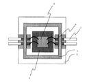
2・・・・・金属基体
3・・・・・貫通金属体
4・・・・・熱拡散金属層
5・・・・・枠体
6・・・・・配線導体
10・・・・蓋体
11・・・・電子部品
12・・・・搭載部
Claims (6)
- 上面の中央部に電子部品を搭載するための搭載部を有する平板状の放熱部材と、該放熱部材の上面に前記搭載部を取り囲んで取着するとともに内面から外面に導出する複数の配線導体を形成して成る枠体とを具備する電子部品収納用パッケージであって、前記放熱部材を、枠状の金属基体の上面に該金属基体よりも熱伝導率の高い熱拡散金属層を積層するとともに、前記金属基体の、前記搭載部の直下で前記枠体の内面よりも内側に位置する部位に形成された貫通孔に前記金属基体よりも熱伝導率の高い貫通金属体を充填することにより形成し、さらに前記金属基体および前記枠体の熱膨張係数を前記熱拡散金属層よりも小さくしており、前記電子部品が搭載される上面とは反対側の、前記貫通金属体の下面の算術平均粗さがRa≦30μmであるとともに、前記放熱部材の反りが下側に凸形状であることを特徴とする電子部品収納用パッケージ。
- 前記枠体の熱膨張係数を前記金属基体よりも小さくしたことを特徴とする請求項1記載の電子部品収納用パッケージ。
- 前記枠体の厚みを前記金属基体よりも薄くしたことを特徴とする請求項1記載の電子部品収納用パッケージ。
- 請求項1乃至請求項3のいずれかに記載の電子部品収納用パッケージと、前記搭載部に搭載するとともに電極を前記配線導体に電気的に接続した前記電子部品と、前記枠体の上面に前記電子部品を覆うように取着した蓋体または前記枠体の内側に前記電子部品を覆うように充填した封止樹脂とを具備していることを特徴とする電子装置。
- 請求項4記載の電子装置を外部放熱板に実装した実装構造であって、前記金属基体の下面および前記貫通金属体の下面を前記外部放熱板に接触させたことを特徴とする電子装置の実装構造。
- 前記貫通金属体の下面と外部放熱板との間にカーボンシートまたはグリースを介在させたことを特徴とする請求項5記載の電子装置の実装構造。
Priority Applications (2)
| Application Number | Priority Date | Filing Date | Title |
|---|---|---|---|
| JP2005155866A JP4610414B2 (ja) | 2005-03-22 | 2005-05-27 | 電子部品収納用パッケージおよび電子装置ならびに電子装置の実装構造 |
| US11/378,859 US7745914B2 (en) | 2005-03-22 | 2006-03-17 | Package for receiving electronic parts, and electronic device and mounting structure thereof |
Applications Claiming Priority (2)
| Application Number | Priority Date | Filing Date | Title |
|---|---|---|---|
| JP2005081464 | 2005-03-22 | ||
| JP2005155866A JP4610414B2 (ja) | 2005-03-22 | 2005-05-27 | 電子部品収納用パッケージおよび電子装置ならびに電子装置の実装構造 |
Publications (3)
| Publication Number | Publication Date |
|---|---|
| JP2006303400A JP2006303400A (ja) | 2006-11-02 |
| JP2006303400A5 JP2006303400A5 (ja) | 2008-05-15 |
| JP4610414B2 true JP4610414B2 (ja) | 2011-01-12 |
Family
ID=37393340
Family Applications (1)
| Application Number | Title | Priority Date | Filing Date |
|---|---|---|---|
| JP2005155866A Expired - Fee Related JP4610414B2 (ja) | 2005-03-22 | 2005-05-27 | 電子部品収納用パッケージおよび電子装置ならびに電子装置の実装構造 |
Country Status (2)
| Country | Link |
|---|---|
| US (1) | US7745914B2 (ja) |
| JP (1) | JP4610414B2 (ja) |
Cited By (1)
| Publication number | Priority date | Publication date | Assignee | Title |
|---|---|---|---|---|
| WO2018092251A1 (ja) * | 2016-11-17 | 2018-05-24 | 三菱電機株式会社 | 半導体パッケージ |
Families Citing this family (19)
| Publication number | Priority date | Publication date | Assignee | Title |
|---|---|---|---|---|
| JP5112101B2 (ja) * | 2007-02-15 | 2013-01-09 | 株式会社東芝 | 半導体パッケージ |
| JP4558012B2 (ja) * | 2007-07-05 | 2010-10-06 | 株式会社東芝 | 半導体パッケージ用放熱プレート及び半導体装置 |
| US7838985B2 (en) * | 2007-07-12 | 2010-11-23 | Vishay General Semiconductor Llc | Semiconductor assembly that includes a power semiconductor die located on a cell defined by first and second patterned polymer layers |
| US7915728B2 (en) * | 2007-07-12 | 2011-03-29 | Vishay General Semiconductor Llc | Subassembly that includes a power semiconductor die and a heat sink having an exposed surface portion thereof |
| JP2011114219A (ja) * | 2009-11-27 | 2011-06-09 | Kyocera Corp | 素子搭載用部品、実装基体および電子装置 |
| JP5500056B2 (ja) * | 2010-12-06 | 2014-05-21 | 日本電気株式会社 | 赤外線センサパッケージおよび該赤外線センサパッケージを搭載した電子機器 |
| KR101277202B1 (ko) * | 2011-04-25 | 2013-06-20 | 주식회사 코스텍시스 | 메탈 베이스 및 그 제조 방법과 이를 이용한 소자 패키지 |
| EP2560203A1 (en) * | 2011-08-17 | 2013-02-20 | ABB Technology AG | Power semiconductor arrangement |
| CN102403419B (zh) * | 2011-11-09 | 2013-08-21 | 东莞勤上光电股份有限公司 | 一种大功率led散热结构的制作工艺 |
| KR101973395B1 (ko) * | 2012-08-09 | 2019-04-29 | 엘지이노텍 주식회사 | 발광 모듈 |
| JP6193784B2 (ja) * | 2014-02-26 | 2017-09-06 | 京セラ株式会社 | 撮像素子実装用基板及び撮像装置 |
| JP6068649B2 (ja) | 2014-04-23 | 2017-01-25 | 京セラ株式会社 | 電子素子実装用基板および電子装置 |
| JP6502925B2 (ja) | 2014-04-23 | 2019-04-17 | 京セラ株式会社 | 電子素子実装用基板および電子装置 |
| JP6208889B2 (ja) | 2014-09-19 | 2017-10-04 | 京セラ株式会社 | 電子素子実装用基板および電子装置 |
| US9559026B2 (en) | 2015-02-26 | 2017-01-31 | Infineon Technologies Americas Corp. | Semiconductor package having a multi-layered base |
| US20190006254A1 (en) * | 2017-06-30 | 2019-01-03 | Kyocera International, Inc. | Microelectronic package construction enabled through ceramic insulator strengthening and design |
| WO2019168056A1 (ja) * | 2018-02-27 | 2019-09-06 | 京セラ株式会社 | 半導体パッケージ、半導体装置および半導体パッケージの製造方法 |
| US20220044979A1 (en) * | 2020-08-04 | 2022-02-10 | Qorvo Us, Inc. | Hermetic package for high cte mismatch |
| US11929310B2 (en) | 2021-12-09 | 2024-03-12 | Nxp Usa, Inc. | Radio frequency packages containing substrates with coefficient of thermal expansion matched mount pads and associated fabrication methods |
Citations (6)
| Publication number | Priority date | Publication date | Assignee | Title |
|---|---|---|---|---|
| JPH0240940A (ja) * | 1988-07-29 | 1990-02-09 | Ibiden Co Ltd | 混成集積回路パッケージ |
| JPH04284655A (ja) * | 1991-03-13 | 1992-10-09 | Hitachi Ltd | 半導体集積回路装置 |
| JPH07302866A (ja) * | 1994-04-28 | 1995-11-14 | Nippon Steel Corp | 半導体装置および該装置用ヒートスプレッダー |
| JPH0883867A (ja) * | 1994-07-15 | 1996-03-26 | Mitsubishi Materials Corp | 高放熱性セラミックパッケージ |
| JPH0945828A (ja) * | 1995-07-31 | 1997-02-14 | Nec Corp | 半導体装置用パッケージ |
| JP2004247514A (ja) * | 2003-02-13 | 2004-09-02 | Kyocera Corp | 半導体素子収納用パッケージおよび半導体装置 |
Family Cites Families (7)
| Publication number | Priority date | Publication date | Assignee | Title |
|---|---|---|---|---|
| US5175612A (en) * | 1989-12-19 | 1992-12-29 | Lsi Logic Corporation | Heat sink for semiconductor device assembly |
| JPH04348062A (ja) | 1991-01-09 | 1992-12-03 | Sumitomo Electric Ind Ltd | 半導体搭載用放熱基板の製造法と該基板を用いた半導体用パッケージ |
| US5367196A (en) * | 1992-09-17 | 1994-11-22 | Olin Corporation | Molded plastic semiconductor package including an aluminum alloy heat spreader |
| JPH06334074A (ja) | 1993-05-20 | 1994-12-02 | Hitachi Metals Ltd | 半導体装置用基板 |
| KR0163871B1 (ko) * | 1995-11-25 | 1998-12-01 | 김광호 | 하부에 히트 싱크가 부착된 솔더 볼 어레이 패키지 |
| US6921971B2 (en) * | 2003-01-15 | 2005-07-26 | Kyocera Corporation | Heat releasing member, package for accommodating semiconductor element and semiconductor device |
| US7235422B2 (en) * | 2005-02-02 | 2007-06-26 | Agere Systems Inc. | Device packages |
-
2005
- 2005-05-27 JP JP2005155866A patent/JP4610414B2/ja not_active Expired - Fee Related
-
2006
- 2006-03-17 US US11/378,859 patent/US7745914B2/en not_active Expired - Fee Related
Patent Citations (6)
| Publication number | Priority date | Publication date | Assignee | Title |
|---|---|---|---|---|
| JPH0240940A (ja) * | 1988-07-29 | 1990-02-09 | Ibiden Co Ltd | 混成集積回路パッケージ |
| JPH04284655A (ja) * | 1991-03-13 | 1992-10-09 | Hitachi Ltd | 半導体集積回路装置 |
| JPH07302866A (ja) * | 1994-04-28 | 1995-11-14 | Nippon Steel Corp | 半導体装置および該装置用ヒートスプレッダー |
| JPH0883867A (ja) * | 1994-07-15 | 1996-03-26 | Mitsubishi Materials Corp | 高放熱性セラミックパッケージ |
| JPH0945828A (ja) * | 1995-07-31 | 1997-02-14 | Nec Corp | 半導体装置用パッケージ |
| JP2004247514A (ja) * | 2003-02-13 | 2004-09-02 | Kyocera Corp | 半導体素子収納用パッケージおよび半導体装置 |
Cited By (3)
| Publication number | Priority date | Publication date | Assignee | Title |
|---|---|---|---|---|
| WO2018092251A1 (ja) * | 2016-11-17 | 2018-05-24 | 三菱電機株式会社 | 半導体パッケージ |
| JPWO2018092251A1 (ja) * | 2016-11-17 | 2019-03-14 | 三菱電機株式会社 | 半導体パッケージ |
| US10910326B2 (en) | 2016-11-17 | 2021-02-02 | Mitsubishi Electric Corporation | Semiconductor package |
Also Published As
| Publication number | Publication date |
|---|---|
| US7745914B2 (en) | 2010-06-29 |
| JP2006303400A (ja) | 2006-11-02 |
| US20060249835A1 (en) | 2006-11-09 |
Similar Documents
| Publication | Publication Date | Title |
|---|---|---|
| JP4610414B2 (ja) | 電子部品収納用パッケージおよび電子装置ならびに電子装置の実装構造 | |
| JP5091459B2 (ja) | 高放熱型電子部品収納用パッケージの製造方法 | |
| JPWO2007138771A1 (ja) | 半導体装置、電子部品モジュールおよび半導体装置の製造方法 | |
| JP4459031B2 (ja) | 電子部品収納用パッケージおよび電子装置 | |
| JP4514598B2 (ja) | 電子部品収納用パッケージおよび電子装置 | |
| JP2006013420A (ja) | 電子部品収納用パッケージおよび電子装置 | |
| JP2000183253A (ja) | 半導体素子収納用パッケージ | |
| JP4377769B2 (ja) | 電子部品収納用パッケージおよび電子装置 | |
| JP2004296726A (ja) | 放熱部材および半導体素子収納用パッケージおよび半導体装置 | |
| JP2004247514A (ja) | 半導体素子収納用パッケージおよび半導体装置 | |
| JP4377748B2 (ja) | 電子部品収納用パッケージおよび電子装置 | |
| JP2005277382A (ja) | 電子部品収納用パッケージおよび電子装置 | |
| JP4485893B2 (ja) | 電子部品収納用パッケージおよび電子装置 | |
| JP2002222887A (ja) | 半導体素子収納用パッケージ | |
| JP2006041287A (ja) | 電子部品収納用パッケージおよび電子装置 | |
| JP2000183236A (ja) | 半導体素子収納用パッケージ | |
| JP2000183215A (ja) | 半導体素子収納用パッケージ | |
| JP2009170758A (ja) | 高放熱型電子部品収納用パッケージ | |
| JP2006013356A (ja) | 電子部品収納用パッケージおよび電子装置 | |
| JP2005340560A (ja) | 電子部品収納用パッケージおよび電子装置 | |
| KR20130141175A (ko) | 칩 패키지 및 그 제조 방법 | |
| JP2004228415A (ja) | 半導体素子収納用パッケージおよび半導体装置 | |
| JP2011035340A (ja) | 高放熱型電子部品収納用パッケージ | |
| JP2004296723A (ja) | 半導体素子収納用パッケージおよび半導体装置 | |
| JP2000114442A (ja) | 電子部品用パッケージ |
Legal Events
| Date | Code | Title | Description |
|---|---|---|---|
| A621 | Written request for application examination |
Free format text: JAPANESE INTERMEDIATE CODE: A621 Effective date: 20080218 |
|
| A521 | Request for written amendment filed |
Free format text: JAPANESE INTERMEDIATE CODE: A523 Effective date: 20080218 |
|
| A521 | Request for written amendment filed |
Free format text: JAPANESE INTERMEDIATE CODE: A523 Effective date: 20080327 |
|
| A977 | Report on retrieval |
Free format text: JAPANESE INTERMEDIATE CODE: A971007 Effective date: 20100405 |
|
| A131 | Notification of reasons for refusal |
Free format text: JAPANESE INTERMEDIATE CODE: A131 Effective date: 20100413 |
|
| A521 | Request for written amendment filed |
Free format text: JAPANESE INTERMEDIATE CODE: A523 Effective date: 20100611 |
|
| A131 | Notification of reasons for refusal |
Free format text: JAPANESE INTERMEDIATE CODE: A131 Effective date: 20100629 |
|
| A521 | Request for written amendment filed |
Free format text: JAPANESE INTERMEDIATE CODE: A523 Effective date: 20100826 |
|
| TRDD | Decision of grant or rejection written | ||
| A01 | Written decision to grant a patent or to grant a registration (utility model) |
Free format text: JAPANESE INTERMEDIATE CODE: A01 Effective date: 20100914 |
|
| A01 | Written decision to grant a patent or to grant a registration (utility model) |
Free format text: JAPANESE INTERMEDIATE CODE: A01 |
|
| A61 | First payment of annual fees (during grant procedure) |
Free format text: JAPANESE INTERMEDIATE CODE: A61 Effective date: 20101012 |
|
| FPAY | Renewal fee payment (event date is renewal date of database) |
Free format text: PAYMENT UNTIL: 20131022 Year of fee payment: 3 |
|
| R150 | Certificate of patent or registration of utility model |
Free format text: JAPANESE INTERMEDIATE CODE: R150 |
|
| LAPS | Cancellation because of no payment of annual fees |