JP4605880B2 - 半導体装置 - Google Patents
半導体装置 Download PDFInfo
- Publication number
- JP4605880B2 JP4605880B2 JP2000308622A JP2000308622A JP4605880B2 JP 4605880 B2 JP4605880 B2 JP 4605880B2 JP 2000308622 A JP2000308622 A JP 2000308622A JP 2000308622 A JP2000308622 A JP 2000308622A JP 4605880 B2 JP4605880 B2 JP 4605880B2
- Authority
- JP
- Japan
- Prior art keywords
- substrate
- semiconductor device
- glass plate
- light
- adhesive resin
- Prior art date
- Legal status (The legal status is an assumption and is not a legal conclusion. Google has not performed a legal analysis and makes no representation as to the accuracy of the status listed.)
- Expired - Fee Related
Links
Images


Classifications
-
- H—ELECTRICITY
- H01—ELECTRIC ELEMENTS
- H01L—SEMICONDUCTOR DEVICES NOT COVERED BY CLASS H10
- H01L24/00—Arrangements for connecting or disconnecting semiconductor or solid-state bodies; Methods or apparatus related thereto
- H01L24/93—Batch processes
- H01L24/95—Batch processes at chip-level, i.e. with connecting carried out on a plurality of singulated devices, i.e. on diced chips
- H01L24/97—Batch processes at chip-level, i.e. with connecting carried out on a plurality of singulated devices, i.e. on diced chips the devices being connected to a common substrate, e.g. interposer, said common substrate being separable into individual assemblies after connecting
-
- H—ELECTRICITY
- H01—ELECTRIC ELEMENTS
- H01L—SEMICONDUCTOR DEVICES NOT COVERED BY CLASS H10
- H01L2224/00—Indexing scheme for arrangements for connecting or disconnecting semiconductor or solid-state bodies and methods related thereto as covered by H01L24/00
- H01L2224/01—Means for bonding being attached to, or being formed on, the surface to be connected, e.g. chip-to-package, die-attach, "first-level" interconnects; Manufacturing methods related thereto
- H01L2224/26—Layer connectors, e.g. plate connectors, solder or adhesive layers; Manufacturing methods related thereto
- H01L2224/31—Structure, shape, material or disposition of the layer connectors after the connecting process
- H01L2224/32—Structure, shape, material or disposition of the layer connectors after the connecting process of an individual layer connector
- H01L2224/321—Disposition
- H01L2224/32151—Disposition the layer connector connecting between a semiconductor or solid-state body and an item not being a semiconductor or solid-state body, e.g. chip-to-substrate, chip-to-passive
- H01L2224/32221—Disposition the layer connector connecting between a semiconductor or solid-state body and an item not being a semiconductor or solid-state body, e.g. chip-to-substrate, chip-to-passive the body and the item being stacked
- H01L2224/32225—Disposition the layer connector connecting between a semiconductor or solid-state body and an item not being a semiconductor or solid-state body, e.g. chip-to-substrate, chip-to-passive the body and the item being stacked the item being non-metallic, e.g. insulating substrate with or without metallisation
-
- H—ELECTRICITY
- H01—ELECTRIC ELEMENTS
- H01L—SEMICONDUCTOR DEVICES NOT COVERED BY CLASS H10
- H01L2224/00—Indexing scheme for arrangements for connecting or disconnecting semiconductor or solid-state bodies and methods related thereto as covered by H01L24/00
- H01L2224/01—Means for bonding being attached to, or being formed on, the surface to be connected, e.g. chip-to-package, die-attach, "first-level" interconnects; Manufacturing methods related thereto
- H01L2224/42—Wire connectors; Manufacturing methods related thereto
- H01L2224/44—Structure, shape, material or disposition of the wire connectors prior to the connecting process
- H01L2224/45—Structure, shape, material or disposition of the wire connectors prior to the connecting process of an individual wire connector
- H01L2224/45001—Core members of the connector
- H01L2224/4501—Shape
- H01L2224/45012—Cross-sectional shape
- H01L2224/45015—Cross-sectional shape being circular
-
- H—ELECTRICITY
- H01—ELECTRIC ELEMENTS
- H01L—SEMICONDUCTOR DEVICES NOT COVERED BY CLASS H10
- H01L2224/00—Indexing scheme for arrangements for connecting or disconnecting semiconductor or solid-state bodies and methods related thereto as covered by H01L24/00
- H01L2224/01—Means for bonding being attached to, or being formed on, the surface to be connected, e.g. chip-to-package, die-attach, "first-level" interconnects; Manufacturing methods related thereto
- H01L2224/42—Wire connectors; Manufacturing methods related thereto
- H01L2224/44—Structure, shape, material or disposition of the wire connectors prior to the connecting process
- H01L2224/45—Structure, shape, material or disposition of the wire connectors prior to the connecting process of an individual wire connector
- H01L2224/45001—Core members of the connector
- H01L2224/45099—Material
- H01L2224/451—Material with a principal constituent of the material being a metal or a metalloid, e.g. boron (B), silicon (Si), germanium (Ge), arsenic (As), antimony (Sb), tellurium (Te) and polonium (Po), and alloys thereof
- H01L2224/45138—Material with a principal constituent of the material being a metal or a metalloid, e.g. boron (B), silicon (Si), germanium (Ge), arsenic (As), antimony (Sb), tellurium (Te) and polonium (Po), and alloys thereof the principal constituent melting at a temperature of greater than or equal to 950°C and less than 1550°C
- H01L2224/45144—Gold (Au) as principal constituent
-
- H—ELECTRICITY
- H01—ELECTRIC ELEMENTS
- H01L—SEMICONDUCTOR DEVICES NOT COVERED BY CLASS H10
- H01L2224/00—Indexing scheme for arrangements for connecting or disconnecting semiconductor or solid-state bodies and methods related thereto as covered by H01L24/00
- H01L2224/01—Means for bonding being attached to, or being formed on, the surface to be connected, e.g. chip-to-package, die-attach, "first-level" interconnects; Manufacturing methods related thereto
- H01L2224/42—Wire connectors; Manufacturing methods related thereto
- H01L2224/47—Structure, shape, material or disposition of the wire connectors after the connecting process
- H01L2224/48—Structure, shape, material or disposition of the wire connectors after the connecting process of an individual wire connector
- H01L2224/4805—Shape
- H01L2224/4809—Loop shape
- H01L2224/48091—Arched
-
- H—ELECTRICITY
- H01—ELECTRIC ELEMENTS
- H01L—SEMICONDUCTOR DEVICES NOT COVERED BY CLASS H10
- H01L2224/00—Indexing scheme for arrangements for connecting or disconnecting semiconductor or solid-state bodies and methods related thereto as covered by H01L24/00
- H01L2224/01—Means for bonding being attached to, or being formed on, the surface to be connected, e.g. chip-to-package, die-attach, "first-level" interconnects; Manufacturing methods related thereto
- H01L2224/42—Wire connectors; Manufacturing methods related thereto
- H01L2224/47—Structure, shape, material or disposition of the wire connectors after the connecting process
- H01L2224/48—Structure, shape, material or disposition of the wire connectors after the connecting process of an individual wire connector
- H01L2224/481—Disposition
- H01L2224/48151—Connecting between a semiconductor or solid-state body and an item not being a semiconductor or solid-state body, e.g. chip-to-substrate, chip-to-passive
- H01L2224/48221—Connecting between a semiconductor or solid-state body and an item not being a semiconductor or solid-state body, e.g. chip-to-substrate, chip-to-passive the body and the item being stacked
- H01L2224/48225—Connecting between a semiconductor or solid-state body and an item not being a semiconductor or solid-state body, e.g. chip-to-substrate, chip-to-passive the body and the item being stacked the item being non-metallic, e.g. insulating substrate with or without metallisation
- H01L2224/48227—Connecting between a semiconductor or solid-state body and an item not being a semiconductor or solid-state body, e.g. chip-to-substrate, chip-to-passive the body and the item being stacked the item being non-metallic, e.g. insulating substrate with or without metallisation connecting the wire to a bond pad of the item
-
- H—ELECTRICITY
- H01—ELECTRIC ELEMENTS
- H01L—SEMICONDUCTOR DEVICES NOT COVERED BY CLASS H10
- H01L2224/00—Indexing scheme for arrangements for connecting or disconnecting semiconductor or solid-state bodies and methods related thereto as covered by H01L24/00
- H01L2224/01—Means for bonding being attached to, or being formed on, the surface to be connected, e.g. chip-to-package, die-attach, "first-level" interconnects; Manufacturing methods related thereto
- H01L2224/42—Wire connectors; Manufacturing methods related thereto
- H01L2224/47—Structure, shape, material or disposition of the wire connectors after the connecting process
- H01L2224/48—Structure, shape, material or disposition of the wire connectors after the connecting process of an individual wire connector
- H01L2224/481—Disposition
- H01L2224/48151—Connecting between a semiconductor or solid-state body and an item not being a semiconductor or solid-state body, e.g. chip-to-substrate, chip-to-passive
- H01L2224/48221—Connecting between a semiconductor or solid-state body and an item not being a semiconductor or solid-state body, e.g. chip-to-substrate, chip-to-passive the body and the item being stacked
- H01L2224/48245—Connecting between a semiconductor or solid-state body and an item not being a semiconductor or solid-state body, e.g. chip-to-substrate, chip-to-passive the body and the item being stacked the item being metallic
- H01L2224/48247—Connecting between a semiconductor or solid-state body and an item not being a semiconductor or solid-state body, e.g. chip-to-substrate, chip-to-passive the body and the item being stacked the item being metallic connecting the wire to a bond pad of the item
-
- H—ELECTRICITY
- H01—ELECTRIC ELEMENTS
- H01L—SEMICONDUCTOR DEVICES NOT COVERED BY CLASS H10
- H01L2224/00—Indexing scheme for arrangements for connecting or disconnecting semiconductor or solid-state bodies and methods related thereto as covered by H01L24/00
- H01L2224/01—Means for bonding being attached to, or being formed on, the surface to be connected, e.g. chip-to-package, die-attach, "first-level" interconnects; Manufacturing methods related thereto
- H01L2224/42—Wire connectors; Manufacturing methods related thereto
- H01L2224/47—Structure, shape, material or disposition of the wire connectors after the connecting process
- H01L2224/48—Structure, shape, material or disposition of the wire connectors after the connecting process of an individual wire connector
- H01L2224/485—Material
- H01L2224/48505—Material at the bonding interface
- H01L2224/48599—Principal constituent of the connecting portion of the wire connector being Gold (Au)
- H01L2224/486—Principal constituent of the connecting portion of the wire connector being Gold (Au) with a principal constituent of the bonding area being a metal or a metalloid, e.g. boron (B), silicon (Si), germanium (Ge), arsenic (As), antimony (Sb), tellurium (Te) and polonium (Po), and alloys thereof
- H01L2224/48638—Principal constituent of the connecting portion of the wire connector being Gold (Au) with a principal constituent of the bonding area being a metal or a metalloid, e.g. boron (B), silicon (Si), germanium (Ge), arsenic (As), antimony (Sb), tellurium (Te) and polonium (Po), and alloys thereof the principal constituent melting at a temperature of greater than or equal to 950°C and less than 1550°C
- H01L2224/48644—Gold (Au) as principal constituent
-
- H—ELECTRICITY
- H01—ELECTRIC ELEMENTS
- H01L—SEMICONDUCTOR DEVICES NOT COVERED BY CLASS H10
- H01L2224/00—Indexing scheme for arrangements for connecting or disconnecting semiconductor or solid-state bodies and methods related thereto as covered by H01L24/00
- H01L2224/73—Means for bonding being of different types provided for in two or more of groups H01L2224/10, H01L2224/18, H01L2224/26, H01L2224/34, H01L2224/42, H01L2224/50, H01L2224/63, H01L2224/71
- H01L2224/732—Location after the connecting process
- H01L2224/73251—Location after the connecting process on different surfaces
- H01L2224/73265—Layer and wire connectors
-
- H—ELECTRICITY
- H01—ELECTRIC ELEMENTS
- H01L—SEMICONDUCTOR DEVICES NOT COVERED BY CLASS H10
- H01L2224/00—Indexing scheme for arrangements for connecting or disconnecting semiconductor or solid-state bodies and methods related thereto as covered by H01L24/00
- H01L2224/80—Methods for connecting semiconductor or other solid state bodies using means for bonding being attached to, or being formed on, the surface to be connected
- H01L2224/85—Methods for connecting semiconductor or other solid state bodies using means for bonding being attached to, or being formed on, the surface to be connected using a wire connector
- H01L2224/8538—Bonding interfaces outside the semiconductor or solid-state body
- H01L2224/85399—Material
- H01L2224/854—Material with a principal constituent of the material being a metal or a metalloid, e.g. boron (B), silicon (Si), germanium (Ge), arsenic (As), antimony (Sb), tellurium (Te) and polonium (Po), and alloys thereof
- H01L2224/85438—Material with a principal constituent of the material being a metal or a metalloid, e.g. boron (B), silicon (Si), germanium (Ge), arsenic (As), antimony (Sb), tellurium (Te) and polonium (Po), and alloys thereof the principal constituent melting at a temperature of greater than or equal to 950°C and less than 1550°C
- H01L2224/85444—Gold (Au) as principal constituent
-
- H—ELECTRICITY
- H01—ELECTRIC ELEMENTS
- H01L—SEMICONDUCTOR DEVICES NOT COVERED BY CLASS H10
- H01L2224/00—Indexing scheme for arrangements for connecting or disconnecting semiconductor or solid-state bodies and methods related thereto as covered by H01L24/00
- H01L2224/93—Batch processes
- H01L2224/95—Batch processes at chip-level, i.e. with connecting carried out on a plurality of singulated devices, i.e. on diced chips
- H01L2224/97—Batch processes at chip-level, i.e. with connecting carried out on a plurality of singulated devices, i.e. on diced chips the devices being connected to a common substrate, e.g. interposer, said common substrate being separable into individual assemblies after connecting
-
- H—ELECTRICITY
- H01—ELECTRIC ELEMENTS
- H01L—SEMICONDUCTOR DEVICES NOT COVERED BY CLASS H10
- H01L2924/00—Indexing scheme for arrangements or methods for connecting or disconnecting semiconductor or solid-state bodies as covered by H01L24/00
- H01L2924/10—Details of semiconductor or other solid state devices to be connected
- H01L2924/11—Device type
- H01L2924/12—Passive devices, e.g. 2 terminal devices
- H01L2924/1203—Rectifying Diode
- H01L2924/12032—Schottky diode
-
- H—ELECTRICITY
- H01—ELECTRIC ELEMENTS
- H01L—SEMICONDUCTOR DEVICES NOT COVERED BY CLASS H10
- H01L2924/00—Indexing scheme for arrangements or methods for connecting or disconnecting semiconductor or solid-state bodies as covered by H01L24/00
- H01L2924/10—Details of semiconductor or other solid state devices to be connected
- H01L2924/11—Device type
- H01L2924/13—Discrete devices, e.g. 3 terminal devices
- H01L2924/1304—Transistor
- H01L2924/1306—Field-effect transistor [FET]
- H01L2924/13091—Metal-Oxide-Semiconductor Field-Effect Transistor [MOSFET]
-
- H—ELECTRICITY
- H01—ELECTRIC ELEMENTS
- H01L—SEMICONDUCTOR DEVICES NOT COVERED BY CLASS H10
- H01L2924/00—Indexing scheme for arrangements or methods for connecting or disconnecting semiconductor or solid-state bodies as covered by H01L24/00
- H01L2924/15—Details of package parts other than the semiconductor or other solid state devices to be connected
- H01L2924/161—Cap
- H01L2924/1615—Shape
- H01L2924/16195—Flat cap [not enclosing an internal cavity]
-
- H—ELECTRICITY
- H01—ELECTRIC ELEMENTS
- H01L—SEMICONDUCTOR DEVICES NOT COVERED BY CLASS H10
- H01L2924/00—Indexing scheme for arrangements or methods for connecting or disconnecting semiconductor or solid-state bodies as covered by H01L24/00
- H01L2924/19—Details of hybrid assemblies other than the semiconductor or other solid state devices to be connected
- H01L2924/191—Disposition
- H01L2924/19101—Disposition of discrete passive components
- H01L2924/19107—Disposition of discrete passive components off-chip wires
Landscapes
- Engineering & Computer Science (AREA)
- Computer Hardware Design (AREA)
- Microelectronics & Electronic Packaging (AREA)
- Power Engineering (AREA)
- Dot-Matrix Printers And Others (AREA)
- Laser Beam Printer (AREA)
- Laser Beam Processing (AREA)
Description
【発明の属する技術分野】
本発明は特に高周波用途の半導体素子および過電流保護機能を気密中空パッケージに収納した半導体装置およびその製造方法に関する。
【0002】
【従来の技術】
図11に従来の中空パッケージを用いた半導体装置の一例を示した。この電子部品は、セラミックなどからなるベース基板1、外部接続用のリード2、同じくセラミック等からなるキャップ3からなり、リード2の素子搭載部4表面に半導体チップ5を固着し、半導体チップ5とリード2とをボンディングワイヤ6で接続し、半導体チップ5をキャップ3が構成する気密空間7内部に封止したものである(例えば、特開平10−173117号)。
【0003】
斯かる部品を製造するときは、リード2をリードフレームの状態で供給し、該リードフレームに対して半導体チップ5をダイボンド、ワイヤボンドし、そしてリードフレーム下面にベース基板1を貼り付け、そしてリード2を挟むようにしてキャップ3をベース基板1に貼り付け、そしてリード2を切断、整形するという工程を経る。
【0004】
【発明が解決しようとする課題】
しかしながら、従来の半導体装置の製造方法では、半導体装置への製造品名、ロット番号、特性等のレーザー印刷工程では、上記した工程により個々に製造された半導体装置にそれぞれ1個ずつ製造品名、ロット番号、特性等をレーザー印刷していた。
【0005】
しかし、本発明の半導体装置への製造品名、ロット番号、特性等のレーザー印刷工程では、基板上に一体に複数個形成された半導体装置に対して、裏面から個々の半導体装置の位置を自動認識し、表面から個々の半導体装置の樹脂層に製造品名、ロット番号、特性等をレーザー印刷する必要があり、従来の半導体装置の製造方法には無い工程であった。
【0006】
【課題を解決するための手段】
上記した各事情に鑑みて成されたものであり、本発明の半導体装置は、絶縁物より成る支持基板と、該支持基板に設けた導電パターンと、前記支持基板の前記導電パターン上に設けた回路素子と、前記回路素子を覆い前記支持基板との間に気密中空部を形成して接着されたガラス板と,前記ガラス板の裏面に塗布した接着樹脂と、前記接着樹脂にレーザ印刷されたマーキングとを有することを特徴とする。
【0007】
本発明の半導体装置は、好適には、気密中空を形成する前記ガラス板の接着面全面にあらかじめ遮光性接着樹脂を被覆しておくことで、半導体装置の製造品名、ロット番号、特性を前記ガラス板の表面から前記遮光性接着樹脂にレーザー印刷することができ、また、印刷された前記半導体装置の製造品名、ロット番号、特性は前記ガラス板で保護されるため消えることがないため、高品質の半導体装置を形成することが可能であることを特徴とする。
【0008】
上記した課題を解決するために、本発明の半導体装置の製造方法は、表面に多数個の搭載部を形成した導電パターンを設け、裏面に外部接続端子を設けた支持基板を準備する工程と、前記各搭載部に回路素子を固着する工程と、前記回路素子を覆い前記支持基板との間に前記各搭載部毎に気密中空部を形成するガラス板の接着面全面に接着樹脂を被覆する工程と、前記ガラス板と前記支持基板とを接着し、前記各搭載部毎に気密中空部を形成する工程と、前記各搭載部毎の前記接着樹脂に前記ガラス板を通してレーザー印刷する工程と、前記支持基板と前記ガラス板との接着部をダイシングして前記各掲載部毎に分離する工程とを有することを特徴とする。
【0009】
更に、本発明の半導体装置の製造方法は、好適には、レーザー印刷工程において、気密中空を形成する前記ガラス板の接着面全面にあらかじめ遮光性接着樹脂を被覆しておくことで、裏面から個々の前記搭載部を自動認識し、表面から個々の前記搭載部に対応する前記接着樹脂に半導体装置の製造品名、ロット番号、特性をそれぞれレーザー印刷することができるため、製造工程が簡素であり、大量生産が可能であることを特徴とする工程である。
【0010】
【発明の実施の形態】
以下に本発明の実施の形態について図面を参照しながら詳細に説明する。
【0011】
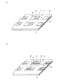
図1は、本発明の半導体装置の1実施例を示す(A)断面図、(B)平面図である。大判基板21から分離された基板21aは、セラミックやガラスエポキシ等の絶縁材料からなり100〜300μmの板厚と、平面視で(図1(B)のように観測して)長辺×短辺が2.5mm×1.9mm程度の矩形形状を有している。基板21aは更に、表面側に第1主面22aを、裏面側に第2主面22bを各々具備し、これらの表面は互いに平行に延在する。柱状部23は基板21aの外周近傍を高さ0.4mm、幅が0.5mm程度で取り囲むように設けられた環状の柱状部であり、柱状部23によって基板21aの中央部分を凹ませた凹部24を形成している。基板21aと柱状部23とは、各々別個に形成された部材を接着剤37で固着したものである。尚、基板21aと柱状部23とがあらかじめ一体化したものであっても良い。
【0012】
基板21aの第1主面22aの表面は平坦に形成されており、その表面には金メッキなどの導電パターンによってアイランド部26と電極部27、28が形成されている。そして、基板21aのアイランド部26には例えばショットキーバリアダイオードやMOSFET素子等の半導体チップ29がダイボンドされている。半導体チップ29の表面に形成した電極パッドと電極部27、28とがボンディングワイヤ30で接続されている。
【0013】
基板21aの第2主面22bの表面には金メッキなどの導電パターンによって外部接続端子32、33、34が形成されている。更に電極部32、33、34には基板21aの第1主面22aから第2主面22bを貫通するビアホール35が設けられる。ビアホール35の内部はタングステン、銀、銅などの導電材料によって埋設されており、アイランド部26を外部接続端子32に、電極部27を外部接続端子33に、電極部28を外部接続端子34に各々電気的に接続する。外部接続端子32、33、34は、その端部が基板21の端部から0.01〜0.1mm程度後退されている。また、電極部27、28のビアホール35上は平坦でないため、ボンディングワイヤ30は、各々電極部27、28のビアホール35上を避けて接続されているのが好ましい。外部接続端子32、33、34は、あらかじめ大判基板21に形成されている。
【0014】
凹部24内部を密閉空間とするため、板厚が0.1〜0.3mm程度の透明なガラス板36が蓋体として用いられる。ガラス板36は、大判基板21上に多数形成された凹部24を被覆するため、ガラス板36の接着面全面には、遮光性接着材37があらかじめ塗布されている。そして、凹部24形成する柱状部23の上部とガラス板36の接着面が接着することにより、半導体チップ29と金属細線30は完全に気密空間内に収納される。
【0015】
ここで、遮光性接着樹脂37がガラス板36の接着面全面に塗布されることで、ガラス板36を透過した光が遮光性接着樹脂37で遮断され、凹部24内部の半導体チップ29等には、光が直接当たらない構造となっている。
【0016】
更に、遮光性接着樹脂37には、表面から個々の搭載部41に対応する部分にレーザー印刷により半導体装置の製造品名、ロット番号、特性が印刷される構造となる。そして、遮光性接着樹脂37上は、ガラス板36により保護されているため、レーザー印刷により印刷された半導体装置の製造品名、ロット番号、特性が消えない構造となる。
【0017】
半導体チップ29周辺は、ダイシングによって切断された柱状部23が取り囲み、更にその上部を切断されたガラス板36が密閉する。柱状部23と基板21aの第1主面22aとが、及び柱状部23とガラス板36とが接着剤37によって接着される。これによって半導体チップ29と金属細線30は凹部24が構成する気密空間内に収納される。基板21a、柱状部23及びガラス板36の外周端面は、ダイシングによって切断された平坦な切断端面となる。
【0018】
上記した半導体装置は、実装基板上の電極パターンに対して外部接続電極32、33、34を対向接着する様にして実装される。
【0019】
次に、図2は、ヒューズを用いた過電流保護装置の実施例を示す(A)断面図、(B)平面図である。基板51はセラミックやガラスエポキシ等の絶縁材料からなる。100〜300μmの板厚と、平面視で(図2(B)のように観測して)長辺×短辺が2.5mm×1.9mm程度の矩形形状を有している。基板51は更に、表面側に第1主面52aを、裏面側に第2主面52bを各々具備する。柱状部53は基板51の外周近傍を高さ0.4mm、幅が0.5mm程度で取り囲むように設けられた環状の側部であり、柱状部53によって基板51の中央部分を凹ませた凹部54を形成している。基板51と柱状部53とは、各々別個に形成された部材を接着剤61固着したものである。尚、基板51と柱状部53とがあらかじめ一体化したものであっても良い。
【0020】
基板51の第1主面52aの表面は平坦に形成されており、その表面には金メッキなどの導電パターンによって電極部55、56が形成されている。電極部55、56間には例えば直径が30μmの金属細線57がワイヤボンドによって打たれている。金属細線57は純度99.99%の金線や、半田の細線等からなり、電極部55に1stボンドが打たれ凹部54の高さに収まる様な高さのワイヤループで電極部56に2ndボンドされる。
【0021】
基板51の第2主面52bの表面には金メッキなどの導電パターンによって外部接続端子58、59が形成されている。更に電極部55、56の下部には基板51を貫通するビアホール60が設けられる。ビアホール60の内部はタングステンなどの導電材料によって埋設されており、電極部55を外部接続端子58に、電極部56を外部接続端子59に各々電気的に接続する。外部接続端子58、59は、その端部が基板51の端部から0.01〜0.1mm程度後退されている。また、電極部27、28のビアホール35上は平坦でないため、ボンディングワイヤ30は、各々電極部27、28のビアホール35上を避けて接続されているのが好ましい。
【0022】
凹部54内部を密閉空間とするため、板厚が0.1〜0.3mm程度の透明なガラス板62が蓋体として用いられる。ガラス板62は、大判基板21上に多数形成された凹部54を被覆するため、ガラス板62の接着面全面には、遮光性接着材61があらかじめ塗布されている。そして、凹部54形成する柱状部53の上部とガラス板62の接着面が接着することにより、金属細線57は完全に気密空間内に収納される。
【0023】
ここで、遮光性接着樹脂61がガラス板62の接着面全面に塗布されることで、ガラス板62を透過した光が遮光性接着樹脂61で遮断され、凹部54内部の金属細線57等には、光が直接当たらない構造となっている。
【0024】
更に、遮光性接着樹脂61には、表面から個々の搭載部63に対応する部分にレーザー印刷により半導体装置の製造品名、ロット番号、特性が印刷される構造となる。そして、遮光性接着樹脂61上は、ガラス板62により保護されているため、レーザー印刷により印刷された半導体装置の製造品名、ロット番号、特性が消えずらい構造となる。
【0025】
上記した過電流保護装置は、実装基板上の電極パターンに対して外部接続電極58、59を対向接着する様にして実装される。外部接続端子58、59間に定格以上の過電流が流れたとき、該過電流は金属細線57を流れ金属細線57の固有抵抗によって急激な温度上昇をもたらす。この発熱により、金属細線57が溶断して過電流に対する保護機能を果たす。上記の直径30μmの金(Au)線であれば、ワイヤ長、約0.7mmの場合、溶断電流は約4A(1〜5秒)となる。多くの場合、放熱性と抵抗の関係から電極部55、56に近い箇所よりは、金属細線57の真中近傍で溶断する。このとき、溶断箇所が樹脂などの他の素材に接していないので、外観上で、装置が発火、発煙、変色、変形することがない装置を得ることが出来る。また、金属細線27が溶断することによって、過電流時に端子間が完全にオープンとなる素子とすることが出来る。
【0026】
尚、ヒューズ素子としては、金属細線の他に電極部55、56を形成する導電パターンの一部をくさび状に幅狭にして連続させたものや、ポリシリコン抵抗体を固着すること等によっても形成することが出来る。要は溶断箇所が凹部54内に収納されていればよい。また、凹部54内部は大気中で密閉するが、例えば窒素雰囲気等の不燃性ガスを充填することも可能である。
【0027】
上記したように、本発明の半導体装置は、気密中空構造を形成する透明なガラス板36の接着面に遮光性接着樹脂37が全面に塗布されることで、レーザー印刷の工程での半導体装置の製造品名、ロット番号、特性が遮光性接着樹脂37の表面に印刷される構造となる。そして、遮光性接着樹脂37上は、ガラス板36により保護されているため、レーザー印刷により印刷された半導体装置の製造品名、ロット番号、特性が、消えることを防止することができる。
【0028】
更に、本発明の半導体装置は、半導体チップ29、ボンディングワイヤ30等を気密中空するのに透明なガラス板36を用いることで、ガラス板36と柱状部23との接着部の状態を外観検査において確認することができる。また、ガラス板36の接着面には、遮光性接着樹脂37が全面に塗布されているため、ガラス板36を透過した光が凹部24内に入射し、半導体チップ29等に直接当たり、半導体チップ29等の特性が劣化することを抑制することができる。
【0029】
以下に図1に示した本発明の第1の実施例を詳細に説明する。
【0030】
第1工程:図3(A)参照
先ず、大判の基板21を準備する。大判基板21はセラミックやガラスエポキシ等の絶縁材料からなり、100〜300μmの板厚を具備する。大判基板21は更に、表面側に第1主面22aを、裏面側に第2主面22bを各々具備する。符号23は高さ0.1〜0.5mm、幅が0.25〜0.5mm程度の一定幅で設けられた格子状の柱状部であり、柱状部23によって基板21の中央部分を凹ませた凹部24を形成している。基板21と柱状部23とは、あらかじめ一体化成形され、柱状部23を含めて上記した板厚となっている。尚、基板21と柱状部23とを個別に形成して接着固定したものを準備しても良い。
【0031】
凹部24は、例えば1つの大きさが約0.8mm×0.6mmの大きさを持ち、基板21に縦横に等間隔で配置されている。凹部24の第1主面22aには多数組のアイランド部26と電極部27、28が金メッキなどの導電パターンにより描画されている。各凹部24とその周囲を囲む第2基板21bの柱状部23の一部が素子搭載部41を構成することになる。
【0032】
第2工程:図3(B)参照
この様な基板21を準備した後、各凹部24毎に、アイランド部26に半導体チップ29をダイボンドし、ボンディングワイヤ30をワイヤボンドする。そして、半導体チップ29にワイヤボンドしたボンディングワイヤ30の片側は、電極部27、28に接続される。このときのボンディングワイヤ30のループ高さは、柱状部23の高さ以下に収まる高さとする。
【0033】
第3工程:図4(A)、(B)参照
板厚が0.1〜0.3mm程度の透明なガラス板36を準備し、ガラス板36の接着面全面に遮光性接着樹脂37を塗布する。そして、ガラス板36は、例えば、大判基板21と柱状部23とを用いることで形成される複数の凹部24を含めた搭載部41上に気密中空構造を構成する蓋体として接着される。これによって半導体チップ29とボンディングワイヤ30は完全に気密空間内に収納される。このとき、上記したように、ガラス板36には、全面に遮光性接着樹脂37が塗布されているため、一度に大量の半導体素子を形成することができる。
【0034】
ここで、大判基板21と柱状部23とは、後から柱状部23を接着してもいいし、あらかじめ一体となって形成されていても良い。また、大判基板21を掘削することによって凹部24を形成しても良い。
【0035】
その後、柱状部23とガラス板36とが接着不良を起こしているかどうかを目視によるチェックが行われる。
【0036】
第4工程:図5(A)、(B)参照
次に、ガラス板36が接着されたことで、大判基板21上には多数の半導体素子が形成された。そして、個々の半導体素子に対応する遮光性樹脂37部分にレーザー印刷により半導体装置の製造品名、ロット番号、特性が印刷される。
【0037】
具体的には、大判基板21上にガラス板36が接着された後、大判基板21の裏面が自動認識される。このとき、まず、行および列ごとに複数の分割パターン71が認識され、分割パターン71間の距離を測定し、分割パターン71間を等間隔に分割する。ここで、この分割パターン71の幅は搭載部41間の幅と同じ幅で形成されており、図5(B)に示したように行および列間にそれぞれ1ずつ設けられている。そして、1列ごとの分割ライン72が形成され、行および列方向の複数の分割ライン72とを組み合わせることで個々の搭載部41の位置が認識される。その結果、搭載部41間の境界を認識することのできない表面から個々の搭載部41に対応して、遮光性接着樹脂37の表面に製造品名、ロット番号、特性等が連続してレーザー印刷にてそれぞれ形成される。
【0038】
更に、裏面から個々の搭載部41を自動認識する作業において、複数の搭載部41を有する基板の4角には基準マーク73が4点設けられ、基準マーク73の中心を結ぶ線が分割ライン72の水平および垂直ラインの基準ライン74となっている。その結果、分割ライン72が形成される際、この基準ライン74と比較されることで分割ラインの精度が向上し、搭載部41上からはみ出すことなく製造品名、ロット番号、特性等がレーザー印刷にて遮光性樹脂37上に形成される。
【0039】
第5工程:図6(A)、(B)参照
そして、基板21表面に形成した合わせマークを基準にして、各搭載部41毎に分割して図6(B)に示したような個別の装置を得る。分割にはダイシングブレード42を用い、基板21の裏面側にダイシングシートを貼り付け、基板21とガラス板36とをダイシングライン43に沿って縦横に一括して切断する。尚、ダイシングライン43は柱状部23の中心に位置する。また、ダイシングシートをガラス板36側に貼り付けて第2主面22b側からダイシングしても良い。
【0040】
以下に、図1に示した本発明の第2の実施例を説明する。柱状部23を個別部品として構成した場合である。
【0041】
第1工程:図7(A)参照
先ず、平板状の大判の基板21を準備する。大判基板21はセラミックやガラスエポキシ等の絶縁材料からなり、100〜300μmの板厚を具備する。大判基板21は更に、表面側に第1主面22aを、裏面側に第2主面22bを各々具備する。第1主面22aの表面には多数組のアイランド部26と電極部27、28が金メッキなどの導電パターンにより描画されている。アイランド26と電極部27、28の周囲を囲む領域が素子搭載部41を構成し、該素子搭載部41が等間隔で縦横に多数個配置される。
【0042】
第2工程:図7(B)参照
この様な基板21を準備した後、各素子搭載部41毎に、アイランド部26に半導体チップ29をダイボンドし、ボンディングワイヤ30をワイヤボンドする。そして、半導体チップ29にワイヤボンドしたボンディングワイヤ30の片側は、電極部27、28に接続される。このときのボンディングワイヤ30のループ高さは、凹部24深さ以下に収まる高さとする。
【0043】
第3工程:図8(A)参照
ダイボンド、ワイヤボンドが終了した基板21に対して、素子搭載部41に対応する箇所に凹部24(貫通穴)を持つ第2基板21aを第1主面22a表面に接着固定する。接着にはエポキシ系等の接着剤を用いる。
【0044】
凹部24は例えば1つの大きさが約0.8mm×0.6mmの大きさを持ち、第2基板21bに縦横に等間隔で配置されている。凹部24と凹部24との間には、柱状部23が高さ0.1〜0.2mm、幅が0.2〜0.5mm程度の一定幅で格子状に取り囲む。これで凹部24にアイランド26、半導体チップ29、電極パット27、28等が露出し、これで図3(B)の状態と等価になる。この手法であれば、平板状の基板21に対してダイボンド、ワイヤボンドが出来るので、吸着コレットやボンディングツールと柱状部23との接触がなく、凹部24の寸法を縮小できる。
【0045】
第4工程:図8(B)、(C)参照
板厚が0.1〜0.3mm程度の透明なガラス板36を準備し、ガラス板36の接着面全面に遮光性接着樹脂37を塗布する。そして、ガラス板36は、例えば、大判基板21と柱状部23とを用いることで形成される複数の凹部24を含めた搭載部41上に気密中空構造を構成する蓋体として接着される。これによって半導体チップ29とボンディングワイヤ30は完全に気密空間内に収納される。このとき、上記したように、ガラス板36には、全面に遮光性接着樹脂37が塗布されているため、一度に大量の半導体素子を形成することができる。
【0046】
その後、柱状部23とガラス板36とが接着不良を起こしているかどうかを目視によるチェックが行われる。
【0047】
第5工程:図9(A)、(B)参照
次に、ガラス板36が接着されたことで、大判基板21上には多数の半導体素子が形成された。そして、個々の半導体素子に対応する遮光性樹脂37部分にレーザー印刷により半導体装置の製造品名、ロット番号、特性が印刷される。
【0048】
具体的には、大判基板21上にガラス板36が接着された後、大判基板21の裏面が自動認識される。このとき、まず、行および列ごとに複数の分割パターン71が認識され、分割パターン71間の距離を測定し、分割パターン71間を等間隔に分割する。ここで、この分割パターン71の幅は搭載部41間の幅と同じ幅で形成されており、図5(B)に示したように行および列間にそれぞれ1ずつ設けられている。そして、1列ごとの分割ライン72が形成され、行および列方向の複数の分割ライン72とを組み合わせることで個々の搭載部41の位置が認識される。その結果、搭載部41間の境界を認識することのできない表面から個々の搭載部41に対応して、遮光性接着樹脂37の表面に製造品名、ロット番号、特性等が連続してレーザー印刷にてそれぞれ形成される。
【0049】
更に、裏面から個々の搭載部41を自動認識する作業において、複数の搭載部41を有する基板の4角には基準マーク73が4点設けられ、基準マーク73の中心を結ぶ線が分割ライン72の水平および垂直ラインの基準ライン74となっている。その結果、分割ライン72が形成される際、この基準ライン74と比較されることで分割ラインの精度が向上し、搭載部41上からはみ出すことなく製造品名、ロット番号、特性等がレーザー印刷にて遮光性樹脂37上に形成される。
【0050】
第6工程:図10(A)、(B)参照
そして、基板21表面に形成した合わせマークを基準にして、各搭載部41毎に分割して図10(B)に示したような個別の装置を得る。分割にはダイシングブレード42を用い、基板21の第2主面22b側にダイシングシートを貼り付け、基板21、第2基板21b、及びガラス板36とをダイシングライン43に沿って縦横に一括して切断する。尚、ダイシングライン43は柱状部23の中心に位置する。また、第2主面22b側からダイシングする構成でも良い。
【0051】
【発明の効果】
上記したように、本発明の半導体装置によれば、気密中空構造を形成する透明なガラス板の接着面に遮光性接着樹脂が全面に塗布されることで、レーザー印刷の工程での半導体装置の製造品名、ロット番号、特性が遮光性接着樹脂の表面に印刷される構造となる。そして、遮光性接着樹脂上は、ガラス板により保護されているため、レーザー印刷により印刷された半導体装置の製造品名、ロット番号、特性が、消えることを防止することができる。
【0052】
更に、本発明の半導体装置の製造方法によれば、レーザー印刷工程において、基板の裏面に形成された複数の分割パターンを認識することで、個々の半導体素子間の境界を認識することのできない基板の表面から個々の半導体素子に対応して、遮光性接着樹脂の表面に製造品名、ロット番号、特性等が連続してレーザー印刷にてそれぞれ形成することができるので、製造コストが大幅に低減することができ、また、大量生産をすることができる。
【図面の簡単な説明】
【図1】本発明を説明するための(A)断面図、(B)平面図である。
【図2】本発明を説明するための(A)断面図、(B)平面図である。
【図3】本発明を説明するための(A)斜視図、(B)斜視図である。
【図4】本発明を説明するための(A)断面図、(B)斜視図である。
【図5】本発明を説明するための(A)断面図、(B)平面図である。
【図6】本発明を説明するための(A)斜視図、(B)斜視図である。
【図7】本発明を説明するための(A)斜視図、(B)斜視図である。
【図8】本発明を説明するための(A)斜視図、(B)断面図、(C)斜視図である。
【図9】本発明を説明するための(A)断面図、(B)平面図である。
【図10】本発明を説明するための(A)斜視図、(B)斜視図である。
【図11】従来例を説明するための(A)断面図、(B)平面図である。
Claims (6)
- 絶縁物より成る支持基板と、
前記支持基板の表面に設けた導電パターンと、
前記導電パターンと電気的に接続され前記支持基板の裏面に設けた外部接続端子と、
前記支持基板の前記導電パターン上に設けた回路素子と、
前記回路素子を覆い前記支持基板との間に気密中空部を形成して接着されたガラス板と,
前記ガラス板の裏面全面に塗布した遮光性接着樹脂とを具備することを特徴とする半導体装置。 - 前記遮光性接着樹脂には、レーザー印刷によるマーキングが設けられている請求項1に記載の半導体装置。
- 前記マーキングは、前記半導体装置の製造品名、ロット番号、特性が設けられる請求項2に記載の半導体装置。
- 前記回路素子は、半導体素子あるいはヒューズ素子であることを特徴とする請求項1または請求項2に記載の半導体装置。
- 前記ヒューズ素子は、金属細線、前記導電パターンの一部を幅狭にしたもの、またはポリシリコン抵抗体である請求項4に記載の半導体装置。
- 前記気密中空部には、不燃性ガスが充填される請求項1〜請求項5のいずれかに記載の半導体装置。
Priority Applications (1)
| Application Number | Priority Date | Filing Date | Title |
|---|---|---|---|
| JP2000308622A JP4605880B2 (ja) | 2000-10-10 | 2000-10-10 | 半導体装置 |
Applications Claiming Priority (1)
| Application Number | Priority Date | Filing Date | Title |
|---|---|---|---|
| JP2000308622A JP4605880B2 (ja) | 2000-10-10 | 2000-10-10 | 半導体装置 |
Publications (2)
| Publication Number | Publication Date |
|---|---|
| JP2002118188A JP2002118188A (ja) | 2002-04-19 |
| JP4605880B2 true JP4605880B2 (ja) | 2011-01-05 |
Family
ID=18788902
Family Applications (1)
| Application Number | Title | Priority Date | Filing Date |
|---|---|---|---|
| JP2000308622A Expired - Fee Related JP4605880B2 (ja) | 2000-10-10 | 2000-10-10 | 半導体装置 |
Country Status (1)
| Country | Link |
|---|---|
| JP (1) | JP4605880B2 (ja) |
Families Citing this family (9)
| Publication number | Priority date | Publication date | Assignee | Title |
|---|---|---|---|---|
| DE10229038B4 (de) * | 2002-06-28 | 2013-08-14 | Robert Bosch Gmbh | Verkapptes Mikrostrukturbauelement mit Hochfrequenzdurchführung |
| JP2004152829A (ja) * | 2002-10-29 | 2004-05-27 | Kyocera Corp | 太陽電池モジュール及びその製造方法 |
| JP2005123377A (ja) * | 2003-10-16 | 2005-05-12 | Rohm Co Ltd | 電子機器およびその製造方法 |
| JP2009017454A (ja) * | 2007-07-09 | 2009-01-22 | Kyocera Kinseki Corp | 圧電振動子及び圧電振動子の製造方法 |
| JP2009238782A (ja) * | 2008-03-25 | 2009-10-15 | Fujikura Ltd | 半導体装置及びその製造方法 |
| JP5188329B2 (ja) * | 2008-08-29 | 2013-04-24 | 日本電波工業株式会社 | 圧電デバイス及びその製造方法 |
| JP2015188190A (ja) * | 2014-03-27 | 2015-10-29 | 株式会社大真空 | 圧電デバイスおよび圧電デバイスの製造方法 |
| MY187287A (en) * | 2015-12-16 | 2021-09-19 | Eng Kah Entpr Sdn Bhd | Laser printed photo on glass article method thereof |
| JP7417029B2 (ja) | 2018-12-14 | 2024-01-18 | 日亜化学工業株式会社 | 発光装置及びその製造方法 |
Citations (1)
| Publication number | Priority date | Publication date | Assignee | Title |
|---|---|---|---|---|
| JPS63153539U (ja) * | 1987-03-27 | 1988-10-07 |
Family Cites Families (2)
| Publication number | Priority date | Publication date | Assignee | Title |
|---|---|---|---|---|
| JPH01238046A (ja) * | 1988-03-18 | 1989-09-22 | Hitachi Ltd | 固体撮像装置 |
| JPH0744261B2 (ja) * | 1988-12-28 | 1995-05-15 | 凸版印刷株式会社 | 半導体装置用透明被覆体 |
-
2000
- 2000-10-10 JP JP2000308622A patent/JP4605880B2/ja not_active Expired - Fee Related
Patent Citations (1)
| Publication number | Priority date | Publication date | Assignee | Title |
|---|---|---|---|---|
| JPS63153539U (ja) * | 1987-03-27 | 1988-10-07 |
Also Published As
| Publication number | Publication date |
|---|---|
| JP2002118188A (ja) | 2002-04-19 |
Similar Documents
| Publication | Publication Date | Title |
|---|---|---|
| JP4565727B2 (ja) | 半導体装置の製造方法 | |
| KR100378278B1 (ko) | 전자 부품 | |
| KR100241573B1 (ko) | 반도체 웨이퍼 | |
| US6365433B1 (en) | Semiconductor device and manufacturing method thereof | |
| JP5930893B2 (ja) | 半導体発光装置の製造方法 | |
| JP4605880B2 (ja) | 半導体装置 | |
| JPH0454973B2 (ja) | ||
| JP4565728B2 (ja) | 中空気密パッケージ型の半導体装置 | |
| JP3462806B2 (ja) | 半導体装置およびその製造方法 | |
| JP3269025B2 (ja) | 半導体装置とその製造方法 | |
| JP2002110833A (ja) | 半導体装置およびその製造方法 | |
| JPH06261448A (ja) | 通信装置用保安器 | |
| JP2000156434A (ja) | 半導体装置 | |
| JP2000232183A (ja) | 半導体装置の製造方法 | |
| JPH11191562A (ja) | 半導体装置の製造方法 | |
| JP4475788B2 (ja) | 半導体装置の製造方法 | |
| JP3247544B2 (ja) | 半導体装置 | |
| JPH11163007A (ja) | 半導体装置の製造方法 | |
| JPH11176856A (ja) | 半導体装置の製造方法 | |
| JP3639509B2 (ja) | 半導体装置の製造方法 | |
| JP2001044313A (ja) | 半導体装置の製造方法 | |
| JP2005229010A (ja) | 半導体装置及びその製造方法 | |
| JP2002373565A (ja) | 保護装置およびその製造方法 |
Legal Events
| Date | Code | Title | Description |
|---|---|---|---|
| RD01 | Notification of change of attorney |
Free format text: JAPANESE INTERMEDIATE CODE: A7421 Effective date: 20051226 |
|
| A621 | Written request for application examination |
Free format text: JAPANESE INTERMEDIATE CODE: A621 Effective date: 20071009 |
|
| A977 | Report on retrieval |
Free format text: JAPANESE INTERMEDIATE CODE: A971007 Effective date: 20091028 |
|
| A131 | Notification of reasons for refusal |
Free format text: JAPANESE INTERMEDIATE CODE: A131 Effective date: 20091110 |
|
| A521 | Written amendment |
Free format text: JAPANESE INTERMEDIATE CODE: A523 Effective date: 20100105 |
|
| TRDD | Decision of grant or rejection written | ||
| A01 | Written decision to grant a patent or to grant a registration (utility model) |
Free format text: JAPANESE INTERMEDIATE CODE: A01 Effective date: 20100907 |
|
| A01 | Written decision to grant a patent or to grant a registration (utility model) |
Free format text: JAPANESE INTERMEDIATE CODE: A01 |
|
| A61 | First payment of annual fees (during grant procedure) |
Free format text: JAPANESE INTERMEDIATE CODE: A61 Effective date: 20101005 |
|
| FPAY | Renewal fee payment (event date is renewal date of database) |
Free format text: PAYMENT UNTIL: 20131015 Year of fee payment: 3 |
|
| R250 | Receipt of annual fees |
Free format text: JAPANESE INTERMEDIATE CODE: R250 |
|
| LAPS | Cancellation because of no payment of annual fees |