JP4550191B2 - Wide viewing angle LCD - Google Patents
Wide viewing angle LCD Download PDFInfo
- Publication number
- JP4550191B2 JP4550191B2 JP33059599A JP33059599A JP4550191B2 JP 4550191 B2 JP4550191 B2 JP 4550191B2 JP 33059599 A JP33059599 A JP 33059599A JP 33059599 A JP33059599 A JP 33059599A JP 4550191 B2 JP4550191 B2 JP 4550191B2
- Authority
- JP
- Japan
- Prior art keywords
- fringe field
- field forming
- liquid crystal
- pixel electrode
- display device
- Prior art date
- Legal status (The legal status is an assumption and is not a legal conclusion. Google has not performed a legal analysis and makes no representation as to the accuracy of the status listed.)
- Expired - Fee Related
Links
Images


Classifications
-
- G—PHYSICS
- G02—OPTICS
- G02F—OPTICAL DEVICES OR ARRANGEMENTS FOR THE CONTROL OF LIGHT BY MODIFICATION OF THE OPTICAL PROPERTIES OF THE MEDIA OF THE ELEMENTS INVOLVED THEREIN; NON-LINEAR OPTICS; FREQUENCY-CHANGING OF LIGHT; OPTICAL LOGIC ELEMENTS; OPTICAL ANALOGUE/DIGITAL CONVERTERS
- G02F1/00—Devices or arrangements for the control of the intensity, colour, phase, polarisation or direction of light arriving from an independent light source, e.g. switching, gating or modulating; Non-linear optics
- G02F1/01—Devices or arrangements for the control of the intensity, colour, phase, polarisation or direction of light arriving from an independent light source, e.g. switching, gating or modulating; Non-linear optics for the control of the intensity, phase, polarisation or colour
- G02F1/13—Devices or arrangements for the control of the intensity, colour, phase, polarisation or direction of light arriving from an independent light source, e.g. switching, gating or modulating; Non-linear optics for the control of the intensity, phase, polarisation or colour based on liquid crystals, e.g. single liquid crystal display cells
- G02F1/133—Constructional arrangements; Operation of liquid crystal cells; Circuit arrangements
- G02F1/1333—Constructional arrangements; Manufacturing methods
- G02F1/1343—Electrodes
- G02F1/134309—Electrodes characterised by their geometrical arrangement
-
- G—PHYSICS
- G02—OPTICS
- G02F—OPTICAL DEVICES OR ARRANGEMENTS FOR THE CONTROL OF LIGHT BY MODIFICATION OF THE OPTICAL PROPERTIES OF THE MEDIA OF THE ELEMENTS INVOLVED THEREIN; NON-LINEAR OPTICS; FREQUENCY-CHANGING OF LIGHT; OPTICAL LOGIC ELEMENTS; OPTICAL ANALOGUE/DIGITAL CONVERTERS
- G02F1/00—Devices or arrangements for the control of the intensity, colour, phase, polarisation or direction of light arriving from an independent light source, e.g. switching, gating or modulating; Non-linear optics
- G02F1/01—Devices or arrangements for the control of the intensity, colour, phase, polarisation or direction of light arriving from an independent light source, e.g. switching, gating or modulating; Non-linear optics for the control of the intensity, phase, polarisation or colour
- G02F1/13—Devices or arrangements for the control of the intensity, colour, phase, polarisation or direction of light arriving from an independent light source, e.g. switching, gating or modulating; Non-linear optics for the control of the intensity, phase, polarisation or colour based on liquid crystals, e.g. single liquid crystal display cells
- G02F1/133—Constructional arrangements; Operation of liquid crystal cells; Circuit arrangements
- G02F1/136—Liquid crystal cells structurally associated with a semi-conducting layer or substrate, e.g. cells forming part of an integrated circuit
-
- G—PHYSICS
- G02—OPTICS
- G02F—OPTICAL DEVICES OR ARRANGEMENTS FOR THE CONTROL OF LIGHT BY MODIFICATION OF THE OPTICAL PROPERTIES OF THE MEDIA OF THE ELEMENTS INVOLVED THEREIN; NON-LINEAR OPTICS; FREQUENCY-CHANGING OF LIGHT; OPTICAL LOGIC ELEMENTS; OPTICAL ANALOGUE/DIGITAL CONVERTERS
- G02F1/00—Devices or arrangements for the control of the intensity, colour, phase, polarisation or direction of light arriving from an independent light source, e.g. switching, gating or modulating; Non-linear optics
- G02F1/01—Devices or arrangements for the control of the intensity, colour, phase, polarisation or direction of light arriving from an independent light source, e.g. switching, gating or modulating; Non-linear optics for the control of the intensity, phase, polarisation or colour
- G02F1/13—Devices or arrangements for the control of the intensity, colour, phase, polarisation or direction of light arriving from an independent light source, e.g. switching, gating or modulating; Non-linear optics for the control of the intensity, phase, polarisation or colour based on liquid crystals, e.g. single liquid crystal display cells
- G02F1/133—Constructional arrangements; Operation of liquid crystal cells; Circuit arrangements
- G02F1/1333—Constructional arrangements; Manufacturing methods
- G02F1/1337—Surface-induced orientation of the liquid crystal molecules, e.g. by alignment layers
- G02F1/133707—Structures for producing distorted electric fields, e.g. bumps, protrusions, recesses, slits in pixel electrodes
-
- G—PHYSICS
- G02—OPTICS
- G02F—OPTICAL DEVICES OR ARRANGEMENTS FOR THE CONTROL OF LIGHT BY MODIFICATION OF THE OPTICAL PROPERTIES OF THE MEDIA OF THE ELEMENTS INVOLVED THEREIN; NON-LINEAR OPTICS; FREQUENCY-CHANGING OF LIGHT; OPTICAL LOGIC ELEMENTS; OPTICAL ANALOGUE/DIGITAL CONVERTERS
- G02F1/00—Devices or arrangements for the control of the intensity, colour, phase, polarisation or direction of light arriving from an independent light source, e.g. switching, gating or modulating; Non-linear optics
- G02F1/01—Devices or arrangements for the control of the intensity, colour, phase, polarisation or direction of light arriving from an independent light source, e.g. switching, gating or modulating; Non-linear optics for the control of the intensity, phase, polarisation or colour
- G02F1/13—Devices or arrangements for the control of the intensity, colour, phase, polarisation or direction of light arriving from an independent light source, e.g. switching, gating or modulating; Non-linear optics for the control of the intensity, phase, polarisation or colour based on liquid crystals, e.g. single liquid crystal display cells
- G02F1/133—Constructional arrangements; Operation of liquid crystal cells; Circuit arrangements
- G02F1/1333—Constructional arrangements; Manufacturing methods
- G02F1/1343—Electrodes
- G02F1/134309—Electrodes characterised by their geometrical arrangement
- G02F1/134336—Matrix
-
- G—PHYSICS
- G02—OPTICS
- G02F—OPTICAL DEVICES OR ARRANGEMENTS FOR THE CONTROL OF LIGHT BY MODIFICATION OF THE OPTICAL PROPERTIES OF THE MEDIA OF THE ELEMENTS INVOLVED THEREIN; NON-LINEAR OPTICS; FREQUENCY-CHANGING OF LIGHT; OPTICAL LOGIC ELEMENTS; OPTICAL ANALOGUE/DIGITAL CONVERTERS
- G02F1/00—Devices or arrangements for the control of the intensity, colour, phase, polarisation or direction of light arriving from an independent light source, e.g. switching, gating or modulating; Non-linear optics
- G02F1/01—Devices or arrangements for the control of the intensity, colour, phase, polarisation or direction of light arriving from an independent light source, e.g. switching, gating or modulating; Non-linear optics for the control of the intensity, phase, polarisation or colour
- G02F1/13—Devices or arrangements for the control of the intensity, colour, phase, polarisation or direction of light arriving from an independent light source, e.g. switching, gating or modulating; Non-linear optics for the control of the intensity, phase, polarisation or colour based on liquid crystals, e.g. single liquid crystal display cells
- G02F1/137—Devices or arrangements for the control of the intensity, colour, phase, polarisation or direction of light arriving from an independent light source, e.g. switching, gating or modulating; Non-linear optics for the control of the intensity, phase, polarisation or colour based on liquid crystals, e.g. single liquid crystal display cells characterised by the electro-optical or magneto-optical effect, e.g. field-induced phase transition, orientation effect, guest-host interaction or dynamic scattering
- G02F1/139—Devices or arrangements for the control of the intensity, colour, phase, polarisation or direction of light arriving from an independent light source, e.g. switching, gating or modulating; Non-linear optics for the control of the intensity, phase, polarisation or colour based on liquid crystals, e.g. single liquid crystal display cells characterised by the electro-optical or magneto-optical effect, e.g. field-induced phase transition, orientation effect, guest-host interaction or dynamic scattering based on orientation effects in which the liquid crystal remains transparent
- G02F1/1393—Devices or arrangements for the control of the intensity, colour, phase, polarisation or direction of light arriving from an independent light source, e.g. switching, gating or modulating; Non-linear optics for the control of the intensity, phase, polarisation or colour based on liquid crystals, e.g. single liquid crystal display cells characterised by the electro-optical or magneto-optical effect, e.g. field-induced phase transition, orientation effect, guest-host interaction or dynamic scattering based on orientation effects in which the liquid crystal remains transparent the birefringence of the liquid crystal being electrically controlled, e.g. ECB-, DAP-, HAN-, PI-LC cells
-
- G—PHYSICS
- G02—OPTICS
- G02F—OPTICAL DEVICES OR ARRANGEMENTS FOR THE CONTROL OF LIGHT BY MODIFICATION OF THE OPTICAL PROPERTIES OF THE MEDIA OF THE ELEMENTS INVOLVED THEREIN; NON-LINEAR OPTICS; FREQUENCY-CHANGING OF LIGHT; OPTICAL LOGIC ELEMENTS; OPTICAL ANALOGUE/DIGITAL CONVERTERS
- G02F1/00—Devices or arrangements for the control of the intensity, colour, phase, polarisation or direction of light arriving from an independent light source, e.g. switching, gating or modulating; Non-linear optics
- G02F1/01—Devices or arrangements for the control of the intensity, colour, phase, polarisation or direction of light arriving from an independent light source, e.g. switching, gating or modulating; Non-linear optics for the control of the intensity, phase, polarisation or colour
- G02F1/13—Devices or arrangements for the control of the intensity, colour, phase, polarisation or direction of light arriving from an independent light source, e.g. switching, gating or modulating; Non-linear optics for the control of the intensity, phase, polarisation or colour based on liquid crystals, e.g. single liquid crystal display cells
- G02F1/133—Constructional arrangements; Operation of liquid crystal cells; Circuit arrangements
- G02F1/1333—Constructional arrangements; Manufacturing methods
- G02F1/1337—Surface-induced orientation of the liquid crystal molecules, e.g. by alignment layers
- G02F1/13373—Disclination line; Reverse tilt
-
- G—PHYSICS
- G02—OPTICS
- G02F—OPTICAL DEVICES OR ARRANGEMENTS FOR THE CONTROL OF LIGHT BY MODIFICATION OF THE OPTICAL PROPERTIES OF THE MEDIA OF THE ELEMENTS INVOLVED THEREIN; NON-LINEAR OPTICS; FREQUENCY-CHANGING OF LIGHT; OPTICAL LOGIC ELEMENTS; OPTICAL ANALOGUE/DIGITAL CONVERTERS
- G02F1/00—Devices or arrangements for the control of the intensity, colour, phase, polarisation or direction of light arriving from an independent light source, e.g. switching, gating or modulating; Non-linear optics
- G02F1/01—Devices or arrangements for the control of the intensity, colour, phase, polarisation or direction of light arriving from an independent light source, e.g. switching, gating or modulating; Non-linear optics for the control of the intensity, phase, polarisation or colour
- G02F1/13—Devices or arrangements for the control of the intensity, colour, phase, polarisation or direction of light arriving from an independent light source, e.g. switching, gating or modulating; Non-linear optics for the control of the intensity, phase, polarisation or colour based on liquid crystals, e.g. single liquid crystal display cells
- G02F1/133—Constructional arrangements; Operation of liquid crystal cells; Circuit arrangements
- G02F1/1333—Constructional arrangements; Manufacturing methods
- G02F1/1337—Surface-induced orientation of the liquid crystal molecules, e.g. by alignment layers
- G02F1/133742—Surface-induced orientation of the liquid crystal molecules, e.g. by alignment layers for homeotropic alignment
-
- G—PHYSICS
- G02—OPTICS
- G02F—OPTICAL DEVICES OR ARRANGEMENTS FOR THE CONTROL OF LIGHT BY MODIFICATION OF THE OPTICAL PROPERTIES OF THE MEDIA OF THE ELEMENTS INVOLVED THEREIN; NON-LINEAR OPTICS; FREQUENCY-CHANGING OF LIGHT; OPTICAL LOGIC ELEMENTS; OPTICAL ANALOGUE/DIGITAL CONVERTERS
- G02F1/00—Devices or arrangements for the control of the intensity, colour, phase, polarisation or direction of light arriving from an independent light source, e.g. switching, gating or modulating; Non-linear optics
- G02F1/01—Devices or arrangements for the control of the intensity, colour, phase, polarisation or direction of light arriving from an independent light source, e.g. switching, gating or modulating; Non-linear optics for the control of the intensity, phase, polarisation or colour
- G02F1/13—Devices or arrangements for the control of the intensity, colour, phase, polarisation or direction of light arriving from an independent light source, e.g. switching, gating or modulating; Non-linear optics for the control of the intensity, phase, polarisation or colour based on liquid crystals, e.g. single liquid crystal display cells
- G02F1/133—Constructional arrangements; Operation of liquid crystal cells; Circuit arrangements
- G02F1/1333—Constructional arrangements; Manufacturing methods
- G02F1/1343—Electrodes
- G02F1/134309—Electrodes characterised by their geometrical arrangement
- G02F1/134318—Electrodes characterised by their geometrical arrangement having a patterned common electrode
-
- G—PHYSICS
- G02—OPTICS
- G02F—OPTICAL DEVICES OR ARRANGEMENTS FOR THE CONTROL OF LIGHT BY MODIFICATION OF THE OPTICAL PROPERTIES OF THE MEDIA OF THE ELEMENTS INVOLVED THEREIN; NON-LINEAR OPTICS; FREQUENCY-CHANGING OF LIGHT; OPTICAL LOGIC ELEMENTS; OPTICAL ANALOGUE/DIGITAL CONVERTERS
- G02F1/00—Devices or arrangements for the control of the intensity, colour, phase, polarisation or direction of light arriving from an independent light source, e.g. switching, gating or modulating; Non-linear optics
- G02F1/01—Devices or arrangements for the control of the intensity, colour, phase, polarisation or direction of light arriving from an independent light source, e.g. switching, gating or modulating; Non-linear optics for the control of the intensity, phase, polarisation or colour
- G02F1/13—Devices or arrangements for the control of the intensity, colour, phase, polarisation or direction of light arriving from an independent light source, e.g. switching, gating or modulating; Non-linear optics for the control of the intensity, phase, polarisation or colour based on liquid crystals, e.g. single liquid crystal display cells
- G02F1/133—Constructional arrangements; Operation of liquid crystal cells; Circuit arrangements
- G02F1/1333—Constructional arrangements; Manufacturing methods
- G02F1/1343—Electrodes
- G02F1/134309—Electrodes characterised by their geometrical arrangement
- G02F1/134345—Subdivided pixels, e.g. for grey scale or redundancy
-
- G—PHYSICS
- G02—OPTICS
- G02F—OPTICAL DEVICES OR ARRANGEMENTS FOR THE CONTROL OF LIGHT BY MODIFICATION OF THE OPTICAL PROPERTIES OF THE MEDIA OF THE ELEMENTS INVOLVED THEREIN; NON-LINEAR OPTICS; FREQUENCY-CHANGING OF LIGHT; OPTICAL LOGIC ELEMENTS; OPTICAL ANALOGUE/DIGITAL CONVERTERS
- G02F1/00—Devices or arrangements for the control of the intensity, colour, phase, polarisation or direction of light arriving from an independent light source, e.g. switching, gating or modulating; Non-linear optics
- G02F1/01—Devices or arrangements for the control of the intensity, colour, phase, polarisation or direction of light arriving from an independent light source, e.g. switching, gating or modulating; Non-linear optics for the control of the intensity, phase, polarisation or colour
- G02F1/13—Devices or arrangements for the control of the intensity, colour, phase, polarisation or direction of light arriving from an independent light source, e.g. switching, gating or modulating; Non-linear optics for the control of the intensity, phase, polarisation or colour based on liquid crystals, e.g. single liquid crystal display cells
- G02F1/133—Constructional arrangements; Operation of liquid crystal cells; Circuit arrangements
- G02F1/1333—Constructional arrangements; Manufacturing methods
- G02F1/1343—Electrodes
- G02F1/134309—Electrodes characterised by their geometrical arrangement
- G02F1/134372—Electrodes characterised by their geometrical arrangement for fringe field switching [FFS] where the common electrode is not patterned
-
- G—PHYSICS
- G02—OPTICS
- G02F—OPTICAL DEVICES OR ARRANGEMENTS FOR THE CONTROL OF LIGHT BY MODIFICATION OF THE OPTICAL PROPERTIES OF THE MEDIA OF THE ELEMENTS INVOLVED THEREIN; NON-LINEAR OPTICS; FREQUENCY-CHANGING OF LIGHT; OPTICAL LOGIC ELEMENTS; OPTICAL ANALOGUE/DIGITAL CONVERTERS
- G02F2201/00—Constructional arrangements not provided for in groups G02F1/00 - G02F7/00
- G02F2201/12—Constructional arrangements not provided for in groups G02F1/00 - G02F7/00 electrode
- G02F2201/123—Constructional arrangements not provided for in groups G02F1/00 - G02F7/00 electrode pixel
Abstract
Description
【0001】
【発明の属する技術分野】
本発明は広い視野角を有する液晶表示装置に係り、より詳しくは、共通電極と画素電極に一定のパターンを形成することで視野角を広げる方式の液晶表示装置に関する。
【0002】
【従来の技術】
一般に、液晶表示装置は2枚の基板の間に液晶を注入し、ここに加える電場の強さを調節することによって、光透過量を調節する構造からなっている。
【0003】
このうち、垂直配向(vertically aligned:VA)方式の液晶表示装置は、電界が印加されていない状態で液晶分子が基板に対して垂直に配向されているため、直交する偏光板を使用する場合に電界が印加されていない状態で完全に光を遮断することができる。即ち、ノーマリーブラックモード(normally black mode)でオフ(off)状態の輝度が非常に低いので、従来の捩じれネマチック液晶表示装置に比べて高い対比比を得ることができる。しかし、電界が印加された状態で液晶分子の傾く方向が不規則的であるため、上部又は下部の偏光板の偏光方向と液晶分子の長軸方向とが一致する部分が存在し、この部分では液晶分子が光の偏光方向を回転させる機能を発揮しないため、光が偏光板によって全て遮断される。このような部分は画面上に黒く現れて画質を低下させ、このような部分をテクスチャー(texture)という。
【0004】
このような問題を解決するために電極をパターニングする方法が多様に提示されている。しかし、電極をパターニングする従来の方法では応答速度が遅いなどの問題点が依然として存在する。
【0005】
ここで、図面を参照して従来の技術による液晶表示装置における電極パターン及びその問題点を説明する。
【0006】
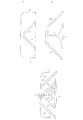
図1は従来の技術による液晶表示装置の上下電極に形成された開口パターンの重畳した状態を示す平面図である。
【0007】
中間が折り曲げられた形態の共通電極の開口パターン1と画素電極の開口パターン2とが互いに対向する形態に配置されており、共通電極と画素電極との間に液晶物質が注入されて各電極の面に対して垂直に配向されている。
【0008】
この時、共通電極と画素電極との間に電界が印加されると、液晶分子3が電気力を受け電極面に対して平行に横になる。このような液晶分子3の電気場に対する反応速度を応答速度といい、開口パターンが図1aのように形成されている場合には応答速度が非常に遅い。その理由は次のようである。
【0009】
即ち、開口パターン1、2によってフリンジフィールド(fringe field)が形成され、液晶分子はフリンジフィールドの電気力を受け、一旦、開口部パターン1、2に対して垂直に配列(A状態)されてから、再び互いに平行になろうとするネマチック(nematic)液晶の本性によって互いに平行に配列(B状態)される2段階動作を行うからである。
【0010】
【発明が解決しようとする課題】
液晶分子の遅い応答速度は動画像表現時に残像を誘発する要因となる。従って、動画像表示の品質を向上させるためには液晶分子の速い応答速度が必要である。
【0011】
本発明は前記課題を解決するためのものであって、その目的は広視野角液晶表示装置の応答速度を向上させることにある。
【0012】
また、本発明の目的は広視野角液晶表示装置の画質を向上させることにある。
【0013】
【課題を解決するための手段】
前記目的を達成するために、本発明の液晶表示装置では、上下の基板で電極の開口部又は突起を、設計規則を守りながらできる限り平行に形成する。
【0014】
以下の液晶表示を提供する。
画素電極を含む第1基板と、
共通電極を含む第2基板と、
前記第1基板と前記第2基板との間に注入されている液晶物質とを含む液晶表示装置であり、
前記画素電極と前記共通電極との間に電圧が印加されていない状態では、前記液晶物質に含まれる液晶分子は前記第1基板と前記第2基板とのいずれに対しても実質的に垂直に配向され、
前記画素電極は、前記画素電極の領域を複数に区切る開口部からなる第1フリンジフィールド形成部と第2フリンジフィールド形成部とを含み、
前記第1フリンジフィールド形成部は、前記画素電極の第1角で交わる第1辺と第2辺との間で、前記第2辺から前記第1辺に向かって、前記第2辺に対して斜めに延び、
前記第2フリンジフィールド形成部は、前記第1角とは異なる前記画素電極の第2角で前記第2辺と交わる前記画素電極の第3辺と前記第2辺との間で、前記第2辺から前記第3辺に向かって、前記第2辺に対して斜めに延び、
前記共通電極は、前記画素電極と対向する前記共通電極の領域を複数に区切る開口部又は突起を含む第3フリンジフィールド形成部と第4フリンジフィールド形成部とを含み、
前記第3フリンジフィールド形成部は、
前記第1辺、前記第2辺、及び前記第1フリンジフィールド形成部で囲まれた前記画素電極の領域に対向する領域を、前記第1辺と前記第2辺との両方に対しては斜めに、前記第1フリンジフィールド形成部に対しては平行に延びている第1中央部、
前記第1辺に沿って前記第1中央部から前記第1角とは反対側に向かって延びている第1横端部、及び、
前記第2辺に沿って前記第1中央部から前記第1角とは反対側に向かって延びている第1縦端部、からなり、
前記第4フリンジフィールド形成部は、前記第2辺と前記第3辺との両方に対しては斜めであり、前記第2フリンジフィールド形成部に対しては平行である第2中央部を含む、
液晶表示装置。
【0015】
ここで、前記第1辺は前記第2辺に対して垂直であり、前記第1中央部は、前記第1辺に対向する前記共通電極の領域から、前記第2辺に対向する前記共通電極の領域まで延びている。
【0016】
ここで、前記第1辺は前記第2辺より短く、前記第1中央部は、前記第1辺に対向する前記共通電極の領域から、前記第2辺に対向する前記共通電極の領域まで延びている。
【0017】
ここで、前記第4フリンジフィールド形成部は、前記第2辺、前記第3辺、及び前記第2フリンジフィールド形成部で囲まれた前記画素電極の領域に対向する前記共通電極の領域に含まれ、前記第4フリンジフィールド形成部は、前記第2辺に沿って前記第2中央部から前記第2角とは反対側に向かって延びている第2縦端部を含む。
【0018】
ここで、前記第4フリンジフィールド形成部は、前記第2辺、前記第3辺、及び前記第2フリンジフィールド形成部で囲まれた前記画素電極の領域に対向する前記共通電極の領域に含まれ、前記第4フリンジフィールド形成部は、前記第3辺に沿って前記第2中央部から前記第2角とは反対側に向かって延びている第2横端部を含む。
【0019】
ここで、前記第1フリンジフィールド形成部、前記第2フリンジフィールド形成部、前記第3フリンジフィールド形成部、及び前記第4フリンジフィールド形成部は一つの画素領域に含まれ、前記第1フリンジフィールド形成部と前記第2フリンジフィールド形成部とは、隣接する画素領域に含まれている第1フリンジフィールド形成部と第2フリンジフィールド形成部とから分離され、又は、前記第3フリンジフィールド形成部と前記第4フリンジフィールド形成部とは、隣接する画素領域に含まれている第3フリンジフィールド形成部と第4フリンジフィールド形成部とから分離されている。
【0020】
ここで、前記第3フリンジフィールド形成部と前記第4フリンジフィールド形成部とは前記第2辺の中心に対して対称である。
【0021】
ここで、前記第1フリンジフィールド形成部と前記第2フリンジフィールド形成部とは開口部からなり、前記第3フリンジフィールド形成部と前記第4フリンジフィールド形成部とは突起からなる。
【0022】
ここで、前記共通電極は、前記第3フリンジフィールド形成部と前記第4フリンジフィールド形成部との間に開口部又は突起からなる第5フリンジフィールド形成部を含み、前記第5フリンジフィールド形成部は、前記第1辺に対して実質的に平行に延びている幹部、前記幹部から前記第1フリンジフィールド形成部に対して平行に延びている第1枝部、及び、前記幹部から前記第2フリンジフィールド形成部に対して平行に延びている第2枝部、を含む。
【0023】
ここで、前記第5フリンジフィールド形成部は、前記第1辺に対して実質的に垂直な前記画素電極の第4辺に沿って前記第1枝部の端から斜めに延びている第1枝端部と、前記第4辺に沿って前記第2枝部の端から斜めに延びている第2枝端部と、を含む。
【0024】
ここで、前記第5フリンジフィールド形成部は一つの画素領域に含まれ、隣接する画素領域に含まれている第3フリンジフィールド形成部、第4フリンジフィールド形成部、及び第5フリンジフィールド形成部から分離されている。
【0030】
【発明の実施の形態】
以下、本発明の実施例による液晶表示装置の構造について図面に基づいて説明する。
【0031】
図2は本発明の実施例による液晶表示装置の概略的構造を示す断面図である。
【0032】
液晶表示装置は、下部基板10と、これと対向している上部基板20と、下部基板10と上部基板20との間に注入されて基板10、20に対して垂直に配向されている液晶物質30とからなる。
【0033】
ガラスなどの透明な絶縁物質からなる下部基板10上にはITO(indium tin oxide)又はIZO(indium zinc oxide)などの透明な導電物質からなっていて開口パターン(図示しない)を有している画素電極12が形成されており、各画素電極12はスイッチング素子11に連結されて画像信号電圧の印加を受ける。この時、スイッチング素子11としては薄膜トランジスタが使用されるのが普通であり、薄膜トランジスタは走査信号を伝達するゲート線(図示しない)及び画像信号を伝達するデータ線(図示しない)にそれぞれ連結されて走査信号に従って画素電極12をオン(on)又はオフ(off)にする。また、下部基板10の下面には下部偏光板14が付着されている。ここで、画素電極12は反射型液晶表示装置である場合には透明な物質からならなくてもよく、この場合には下部偏光板14も不必要になる。
【0034】
前記下部基板と同様にガラスなどの透明な絶縁物質からなる上部基板20の下面に、光漏れを防止するためのブラックマトリックス21と、赤、緑、青のカラーフィルタ22及びITO又はIZOなどの透明な導電物質からなっており開口(図示しない)を有している共通電極23とが形成されている。この時、ブラックマトリックス21やカラーフィルタ22は下部基板10上に形成されることも可能である。また、上部基板20の上面には上部偏光板24が付着されている。
【0035】
下部偏光板14及び上部偏光板24の偏光方向は、ノーマリーブラックモード(normally black mode)では互いに直交するように配置し、ノーマリーホワイトモード(normally white mode)では互いに平行に配置する。以下ではノーマリーブラックモードのみを考慮する。
【0036】
2枚の基板10、20の外側偏光板14、24の内側には補償フィルム15、25がそれぞれ付着されている。この時、2枚の基板のうちの一側にはaプレート一軸性補償フィルムを付着して反対側にはcプレート一軸性補償フィルムを付着したり、cプレート一軸性補償フィルムを両側に付着することができる。一軸性補償フィルムの代わりに二軸性補償フィルムを使用することもできるが、この場合は2枚の基板のうちの一側のみに二軸性補償フィルムを付着することもできる。補償フィルムの付着方向はaプレート又は二軸性補償フィルムにおいて屈折率が最大の方向、即ち、遅い軸(slow axis)が偏光板の透過軸と一致するか直交するように付着する。
【0037】
次いで、図面を参照して本発明の実施例による液晶表示装置の画素電極及び共通電極の開口パターンについて説明する。
【0038】
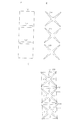
図3a及び3bはそれぞれ本発明の第1及び第2実施例による液晶表示装置の上下電極に形成された開口パターンの重畳した状態を示す平面図である。
【0039】
応答速度を向上させるためには、図3aのように、開口パターン1、2を平行な直線に形成して、液晶分子3がフリンジフィールドによって配列された状態が液晶分子相互間で平行な状態になるようにする。こうすると、1段階動作で液晶分子の動きが完了するために応答速度が速くなる。
【0040】
しかし、図3aのように開口パターン1、2を形成した場合には、テクスチャー(texture)が広い範囲にかけて著しく発生する。また、白残像(明るい色の地に暗い色を表示してから再び明るい色の地に戻る時に瞬間的に周辺の地の色よりもっと明るくなる現象)が発生する可能性がある。
【0041】
このような問題点を改善するために、図3bに示されているように、緩やかな曲線形の開口パターン1、2を考慮することができる。しかし、このような形態では液晶分子が完全な1段階動作を行えないため、再び動作速度が遅くなるという問題点が発生する。
【0042】
以下、動作速度の向上及びテクスチャーなどの不良の抑制の両方を考慮してデザインされた開口パターンについて説明する。
【0043】
図4a、5a、6a、7a、8a、9a、10aはそれぞれ本発明の第3ないし第9実施例による液晶表示装置の画素電極のパターンを示す平面図であり、図4b、5b、6b、7b、8b、9b、10bはそれぞれ本発明の第3ないし第9実施例による液晶表示装置の共通電極に形成されている開口パターンを示す平面図であり、図4c、5c、6c、7c、8c、9c、10cはそれぞれ本発明の第3ないし第9実施例による液晶表示装置の上下基板を整列させた状態で画素電極のパターンと共通電極の開口パターンとを重畳させた状態の平面図である。
【0044】
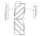
まず、本発明の第3実施例について説明する。
図4aに示されているように、長方形の画素電極12の中間部に右辺から左側に細く掘られた第1開口部121が形成されており、第1開口部121の入口の両側は角が切り取られて緩やかな角度で曲がっている(以下、“角取り”という)。第1開口部121を中心にして画素電極12を上部と下部とに区分すると、上部及び下部にはそれぞれ第2及び第3開口部122、123が形成されている。第2及び第3開口部はそれぞれ画素電極12の上部及び下部を対角線に掘り下げて形成されており、互いに対称をなしている。第2及び第3開口部122、123は第1開口部121とは反対方向に掘り下げられていて第1開口部121から遠くなる形態である。
【0045】
図4bに示されているように、共通電極23には、横方向に形成されている幹部211と、幹部211からそれぞれ斜線方向に上下に伸びている第1及び第2枝部212、214と、第1及び第2枝部212、214からそれぞれ縦方向に上下に伸びている第1及び第2枝端部213、215とを含む第4開口部が形成されている。また、共通電極23には、第1枝部212と平行に斜線方向に形成されている中央部221と、中央部221から横方向に伸びている横端部222と、中央部221から縦方向に伸びている縦端部223とを含む第5開口部と、第4開口部に対して第5開口部と対称をなしている第6開口部とが形成されている。このような配置の第4、第5及び第6開口部は共通電極23に反復して形成されている。
【0046】
図4cに示されているように、画素電極12の第1ないし第3開口部121、122、123と共通電極23の第4ないし第6開口部とが重畳して画素電極12を多数の領域に分割している。この時、画素電極12の開口部121、122、123と共通電極23の開口部とは交互に配置されている。第1ないし第6開口部は画素電極12の中央を分割する第1開口部121と、第4開口部の幹部211と、画素電極12の辺と重畳する第4開口部の枝端部213、215と、第2及び第3開口部の横端部222、232及び縦端部223、233以外は、大部分の領域で互いに平行に形成されている。
【0047】
この時、上下偏光板14、24は偏光方向がそれぞれ横方向(0°)と縦方向(90°)又は縦方向と横方向になるように配置されている。
【0048】
こうすると、図4cに示されているように、電気場の印加によって再配列された液晶分子のうちで偏光板14、24の偏光方向に横になる数が少なくなるためにテクスチャーの発生が減少する。また、フリンジフィールドによって液晶分子が配列された状態が必ず液晶分子が互いに平行な状態であるので、1段階動作で液晶分子の動きが完了する。従って、応答速度が非常に速い。さらに、開口部は画素領域で大きく2方向に伸びており、この2方向は互いに90°をなしている。また、上下基板の開口部は互いに交互に配置されているので、フリンジフィールドの方向は1つの画素領域内で4つの方向に分類される。従って、4つの方向全てで広い視野角を得ることができる。
【0049】
本発明の第4実施例について説明する。
図5aに示されているように、画素電極12の右辺から左上側に斜線方向に伸びている第1斜線部121と、第1斜線部121に連結されており右上側斜線方向に伸びている第2斜線部122とを含む第1開口部が形成されており、画素電極12の左側角部分は角取りが行われている。この時、第1斜線部121と第2斜線部122とがぶつかる位置は画素電極12を上部と下部とに両分する中央部である。
【0050】
図5bに示されているように、共通電極23には、縦方向に伸びている基底部211と、基底部211の中央から左側横方向に伸びている横枝部212とを含む第2開口部が形成されている。この時、第2開口部は基底部211と横枝部212とがぶつかる地点から離れるほど幅が狭くなり、基底部211と横枝部212とがぶつかる地点の両側角は角取りが行われている。また、共通電極23には縦方向に形成されている中央部221と、中央部221の両端からそれぞれ右上側と右下側とに伸びている第1及び第2斜線枝部222、223とを含む第3開口部が形成されている。この時、第3開口部は第2開口部に対して上下対称に配置されている。
【0051】
図5cに示されているように、画素電極12の第1開口部と共通電極23の第2及び第3開口部とが重畳して画素電極12を多数の領域に分割している。この時、第1開口部は第2開口部と第3開口部との間に位置する。また、第1ないし第3開口部は、画素電極12を上下に両分する横枝部212と、画素電極12の辺と重畳する基底部211と、中央部221以外は互いに平行に配置されている。画素電極12の左側角及び第2開口部の中心部で角取りを行ったのも開口部を平行に配置するための方法の1つとして行ったものである。
【0052】
この時、上下偏光板14、24は偏光方向が第3実施例と同様になるように配置される。
【0053】
これにより、第3実施例と同様な効果を得ることができる。
【0054】
本発明の第5実施例について説明する。
図6aに示されているように、画素電極12の上側1/3地点に右辺から左側に掘り下げられた第1開口部121と、下側1/3地点に左辺から右側に掘り下げられた第2開口部122とが画素電極12に形成されている。開口部121、122の入口の両側角は角取りが行われており、画素電極12の左上及び右下の角も角取りが行われている。
【0055】
図6bに示されているように、共通電極23には、左下側に伸びている第1斜線部211と、第1斜線部211から折り曲げられて右下側に伸びている第2斜線部212と、第2斜線部212から折り曲げられて左下側に伸びている第3斜線部213とを含む第3開口部が形成されている。
【0056】
図6cに示されているように、第1及び第2開口部によって3つの領域に分割された画素電極12の各領域を第3開口部がそれぞれ2分割している。
【0057】
この時、上下偏光板14、24は偏光方向が第3実施例と同様になるように配置される。
【0058】
本発明の第6実施例について説明する。
図7aに示されているように、画素電極12の上側1/3地点及び下側1/3地点にそれぞれ長方形の第1開口部121及び第2開口部122が形成されて画素電極12を3等分している。
【0059】
図7bに示されているように、X字形の第3ないし第5開口部210、220、230が一定の間隔をおいて上下方向に一列に配置されている。開口部210、220、230のそれぞれの中心の交差部に形成されている角は角取りが行われている。
【0060】
図7cに示されているように、第1及び第2開口部121、122によって3つの領域に等分されている画素電極12の各領域を第3ないし第5開口部210、220、230がそれぞれ4分割している。
【0061】
この時、上下偏光板14、24は、 横方向を基準(0°)にすると、 偏光方向がそれぞれ45°及び135°になるように配置する。
【0062】
本発明の第7実施例について説明する。
図8aに示されているように、画素電極12の上面を左右に2分割する垂直部111と、垂直部111の下端に連結されており画素電極12を上下に分割する水平部112とを含む第1開口部と、水平部112によって分割された画素電極12の下部領域を2分割する長方形の第2開口部120とが画素電極12に形成されている。
【0063】
図8bに示されているように、縦方向に形成されており互いに平行な第3及び第4開口部210、220と、第3及び第4開口部210、220の下部に横方向に形成されており互いに平行な第5及び第6開口部230、240とが共通電極23に形成されている。この時、第5及び第6開口部230、240の両端は幅が次第に拡張されて三角形に形成されている。
【0064】
図8cに示されているように、画素電極12の第1開口部と、共通電極23の第3及び第4開口部210、220とが画素電極12の上面を縦に4等分しており、第2開口部120と第5及び第6開口部230、240とが画素電極12の下面を横に4等分している。
【0065】
この時、上下偏光板14、24は偏光方向が第6実施例と同様になるように配置される。
【0066】
こうすると、開口部は大部分の領域で互いに平行になり、液晶分子が横になる方向も偏光方向と45°をなすようになるので、速い応答速度及びテクスチャーの少ない良好な画質を得ることができる。開口部は画素領域で大きく2つの方向に伸びており、この2つの方向は互いに90°をなしている。また、上下基板の開口部が互いに交互に配置されているのでフリンジフィールドの方向は1つの画素領域内で4つの方向に分類される。
【0067】
本発明の第8実施例について説明する。
図9aに示されているように、画素電極12の下部1/3程度の部分に横方向に長く伸びている第1開口部110が形成されている。
【0068】
図9bに示されているように、縦方向に長く伸びている幹部211及び幹部211の下端に連結されておりそれぞれ右側及び左側に伸びている第1及び第2枝部212、213と、幹部211の上端に連結されており逆三角形に形成されている上端部214とを含む第2開口部と、第2開口部の下部に横方向に長く形成されている第3開口部220とが共通電極23に形成されている。この時、第1及び第2枝部212、213は水平に形成されずに僅かに下側に傾いており、第3開口部220の両端は幅が次第に拡張されて三角形に形成されている。
【0069】
図9cに示されているように、第2開口部によって画素電極12が上面及び下面に分割され、このうちの上面が幹部211によって左右に両分されており、第1開口部110及び第3開口部220によって画素電極12の下面が3分割されている。
【0070】
この時、上下偏光板14、24は偏光方向が第6実施例と同様になるように配置されている。
これによって、第7実施例と類似した効果を得ることができる。
【0071】
最後に本発明の第9実施例について説明する。
図10aに示されているように、画素電極12が楕円4つが一列に連結されている形態に形成されている。
【0072】
図10bに示されているように、共通電極23には4つのひし形の第1開口部210が一定の間隔をおいて一列に配列されており、第1開口部210を囲む形態に第2及び第3開口部220、230が形成されている。第2及び第3開口部220、230の辺のうちで第1開口部210に面している辺は谷が曲線化された鋸の歯形状に形成されており、第1開口部210に対して左右対称をなしており、鋸の歯の山部分は第1開口部210の間に位置するように形成されている。
【0073】
図10cに示されているように、画素電極12をなす各楕円の中央に第1開口部210が位置しており、第2及び第3開口部220、230は画素電極12を囲んでいる。この時、第2及び第3開口部220、230の鋸の歯形状の辺から画素電極12の辺までの距離は一定になるように配置されている。
【0074】
この時、上下偏光板14、24は偏光方向がそれぞれ0°及び90°になるように配置されている。
【0075】
以上の第3ないし第9実施例は、多様な実験の結果から得られた次のような分割配向のための開口部パターンの条件を最大限満たすことができるように開口部パターンを形成したものである。
【0076】
第1に、最も良好な視野角を得るためには、4分割配向された領域が1つの画素内に入っているのがよい。
【0077】
第2に、安定した分割配向を得るためには、分割された微小領域の境界以外のところでディスクリネーション(disclination)や不規則な組織(texture)が発生してはならない。ディスクリネーションは狭い領域で液晶分子の方向子が一定の方向に配列されずに様々な方向に配列されている時に発生し、特に、1つの領域で液晶分子が互いにぶつかる方向に倒れる時に発生する。従って、安定した分割配向を得るためには、上下基板のパターンが反復して形成されるのが有利であり、上板のパターンと下板のパターンとの末端は近ければ近いほどよい。即ち、液晶表示装置を上から見たときに上板のパターンと下板のパターンとによって形成される領域が閉じた多角形に近似した形態になるのがよい。また、1つの領域を形成するために一方の基板に形成されたパターンが鋭角をなす場合にはディスクリネーションが発生しやすいので、パターンは鈍角のみで形成するのがよい。また、安定した分割配向は輝度にも影響を及ぼす原因になる。配向が乱れた領域ではオフ状態で光が漏れるようになると共に、オン状態で周囲の他の部分に比べて暗い状態になり、液晶分子の配列が変化する時に配列の乱れた部分が移動して残像などの原因になることもある。
【0078】
第3に、高輝度を得るためには次のような条件を満たさなければならない。まず、隣接した領域の液晶方向子(director)がなす角は90°になるのが最も好ましい。こうなる時には最も狭い領域のみでディスクリネーションが発生するためであり、偏光板の透過軸と液晶方向子とがなす角が45度をなす時に最も高い輝度を得ることができる。また、上板及び下板にそれぞれ形成されている開口部パターンが折れ曲がったり折れたりする角度が、可能な限り緩慢な(直線に近いほど)のが好ましい。
【0079】
最後に、速い応答速度を得るためには、上板及び下板にそれぞれ形成されている開口部パターンが折れ曲がったり折れたりする角度が、可能な限り緩慢な(直線に近いほど)のが好ましい。即ち、一の字で対向する形態に最も近似するのが応答速度の面で有利である。
【0080】
次いで、開口部パターンの幅及びパターン間の間隔が透過率及び応答速度に及ぼす影響について説明する。
開口部パターンの幅及び間隔による影響を調査するために、図11に示した9つの開口パターンを有するパネルを制作して実験した。
【0081】
図11において斜線で表示したパターンは共通電極の開口部パターンであり、太線で示されたパターンは画素電極の形態である。
【0082】
B、C、DパターンとE、F、Gパターンとはそれぞれパターンの幅及び間隔のみが異なる同一形態のパターンであり、IとJパターンとはパターン間の間隔が異なる。AパターンはB、C、Dパターンと類似しているが、パターン間の間隔が異なる。これら各パターンの幅及び間隔は表1に示されている。
【表1】

図12aは各パターンに対するテストセル(test cell)の光透過率をパーセント(%)で示したグラフであり、図12bはBパターンの光透過率を基準にして他のパターンの光透過率の比を示したグラフである。
【0084】
図12a及び12bのグラフに示されているように、Gパターンの光透過率が約13%で最高であり、その次はE、I、B、D、A、C、F、Jパターンの順である。
【0085】
図13は各パターンを適用したテストセルの階調による応答時間を示すグラフである。実際に適用する時には64階調までのみを使用するが、本実験では110階調まで実験した。
【0086】
図13に示されているように、B、C、D及びJパターンの応答時間が全ての階調で比較的短い。即ち、応答速度が速かった。他のパターンで応答速度が遅い理由はA及びIパターンの場合はテクスチャー移動のためであり、E、F、Gパターンの場合は液晶分子が2段階動作をするためである。
【0087】
表2は図11の9つのパターンを実際のパネルに適用して実験した結果である。各パターンに対して4つのパネルを制作して実験した。
【表2】
実際のパネルの結果もテストセルの結果と類似した。ただし、Iの応答速度がテストセルとは異なって比較的速く、Jパターンの輝度が予想より明るかった(テストセルではJパターンの輝度がBパターンに比べて75%程度であったが、実際のパネルではBパターンに比べて90%であった)。
【0089】
実際のパネルでA、C、I、Jパターンは白残像が現れた。Cパターンでは白残像が強く現れるので問題になるが、I及びJパターンではある程度は改善することができる。
【0090】
以上の結果に基づいて、改善しようとする特性に応じて選択することができるパターンについて説明する。
【0091】
まず、輝度向上及び白残像改善を目的とする場合にはB、D、E、Iパターンが有利であり、輝度を現在の水準以上に維持しながら応答速度を向上しようとする場合にはB、D、Iパターンが好ましく、輝度を犠牲にして応答速度の向上を目的とする場合にはD、Jパターンが有利である。
【0092】
次いで、応答速度と開口部パターンの幅との関係をより明確にするために、形態が同一でパターンの幅が異なるB、C、Dパターンに対して光特性の差について説明する。
【0093】
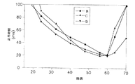
図14は実際のパネルでのB、C、Dパターンそれぞれの階調による応答時間を示すグラフである。
【0094】
20階調から40階調の間における応答時間はD<B<Cの順に長かった。即ち、パターンの幅が大きいほど応答時間が短い。
【0095】
約40階調からはCパターンの応答時間がBパターンより短く、約45階調からはCパターンの応答時間がDパターンよりも短い。しかし、これは白残像現象のために応答時間が短いように見えるだけで、実際に短いのではない。即ち、白残像のために応答波形が歪曲して応答時間が実際より短く見えるのである。従って、このような点を鑑みるとパターンの幅が広いほど応答速度が速くなることがわかる。
【0096】
60階調以上の高い電圧がかかるとテクスチャー不安のために応答速度が急激に遅くなるが、そのうちでは開口部パターンの幅が最も広いDパターンが最も安定した(緩やかに増加)特性を有する。
【0097】
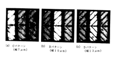
図15はC、B、Dパターンに対する白色階調での顕微鏡写真である。
写真に示されているように、輝度はテクスチャー安定度の低いCが最も暗く、BとDとは近似した明るさを有する。Dは開口部パターンの幅が大きいので開口率は低いがテクスチャー安定度が比較的高い輝度を有する。テクスチャー安定度もフリンジフィールドの強さ及びパターンの幅によって決定されるものと思われる。
【0098】
また、領域の境界部(開口部パターンが形成されている部分)の形態が異なる。Cパターンの場合は領域境界部のほとんどの部分で二股のテクスチャーが鮮明に現れ、Bパターンの場合は微かに二股のテクスチャーが現れるが、Dパターンの場合は領域境界部が1つの黒線として現れる。
【0099】
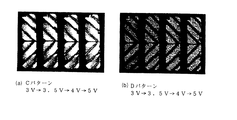
図16はCパターン及びDパターンに対するテストセルの印加電圧別のドメイン分割写真である。
Cパターンの場合は3.5Vから領域境界部に二股のテクスチャーが現れて電圧が高くなるほど鮮明になる。しかし、Dパターンの場合は5Vになってから領域境界部が微かに二股に分かれる。領域境界部が二股に分かれるのはその領域で液晶分子が不均一に配列されるためである。この現象を説明するために、パターンの幅に応じたフリンジフィールドの強さを考察してみる。
【0100】
図17はパターンの幅に応じたフリンジフィールドの強さを示す概念図である。
開口部パターンの幅が広くなるほどフリンジフィールドの水平成分が大きくなる。水平成分は液晶が横になる方向を決定するのに重要な役割を果たす。従って、広い幅の開口部パターンがドメインを形成するのに効果的である。また、開口部の中央の電気場の垂直成分の強さは開口部パターンの幅が広くなるほど弱くなる。
【0101】
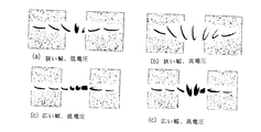
図18は開口部パターンの周辺での液晶分子の配列状態を示す図面である。
開口部パターンの幅が狭い場合には開口部の中心部でも液晶分子がある程度横になる。印加される電圧が低い場合には僅かに傾く程度であるが、電圧が高くなると水平に完全に横になる。これは開口部パターンの中央部でも電気場の垂直成分が強いためである。このために光が漏れるようになり、領域境界部が二股の線に分かれるようになる。また、液晶分子が開口部で横になる方向を180°変更する時、開口部の幅が狭いため弾性力が強い。反面、フリンジフィールドの水平成分は弱いため、弾性力にフリンジフィールドが勝てない。従って、領域境界部での液晶分子の配列が不均一である。このような不均一な液晶分子の配列は画素の小領域の内部まで伝播される。
【0102】
開口部パターンの幅が広い場合には、開口部の中心で液晶分子が垂直に立つ。
印加電圧が強くなるのに伴って液晶分子が僅かに傾くが、その程度は幅が狭い場合に比べて著しくない。従って、漏れる光が少なく、小領域境界部が1つの黒線として現れる。
【0103】
以上のように、開口部パターンの幅が広いほど応答速度が速く、画素の小領域が均一である。開口部パターンの幅が広いと開口率は小さいが液晶分子の配列が均一になるので輝度は良好である。以上の実験によると、開口部パターンの幅は13±3μm程度が適当である。この時、セルギャップ(cell gap)は約4μmないし6μm程度である。
【0104】
以下、開口部パターン間の間隔に応じた光特性について説明する。
IパターンとJパターンはパターンの幅は同一でパターン間の間隔は互いに異なる。テストセルの結果ではIパターンとJパターンとが光特性において顕著な差異を有するが、実際のパネルの結果では大きな差異がない。これは配向膜の種類の差異や保護膜(絶縁膜)の有無の差異、印加される電圧波形の差異などによるものであると推定される。しかし、実際のパネルで動映像の移動速度を比較してみると、IパターンよりJパターンの方が速い(灰色地に黒色で四角形を引いてみれば分かる)。但し、階調によって応答速度に差異がある。
【0105】
開口部パターンの幅においても、パターン間の距離が狭くなると開口率が顕著に減少するが、輝度は大きな差異がない。これはテクスチャーのためである。即ち、パターン間の距離が広くなるとテクスチャー制御が難しくなり、狭くなると制御が容易になる。従って、パターン間の距離が狭くなると開口率は減少するがテクスチャーを適切に制御することができるので輝度は補償される。ただし、Iパターンはパターン間の距離は遠い方であるが、テクスチャー制御が比較的適切に行われているために輝度が高い。
【0106】
結論として、パターン間の間隔を狭くするほど階調応答速度が向上される。輝度は開口率が減少する分だけ低くなる確率が高いが、テクスチャーを制御することによってある程度挽回される。
【0107】
テクスチャーは応答速度と深い関連がある。動くテクスチャーは応答速度を低下させる。高い電圧が印加されると大部分のパターンで応答速度が低下する。これはテクスチャーが発生するためである。従って、テクスチャーを適切に制御すると、画質の向上は勿論、応答速度も向上させ得る。以下でテクスチャーの発生を抑制することができる方法を説明する。
【0108】
図19及び20はそれぞれBパターン及びJパターンでテクスチャーが発生する部分とこれを拡大した図面である。
【0109】
図19の開口部パターンは図4cのパターンとほぼ類似する。ただし、画素電極12に形成されている第2及び第3開口部122、123が図4cとは異なる。即ち、右側辺から始まっている。また、第2及び第3開口部122、123が終わる部分には画素電極を外部に突出させて形成する。これは開口部122、123によって画素電極12の各部分の連結が不良になるのを防止するためである。
【0110】
テクスチャーが発生する部分は主に共通電極の開口部の端部と画素電極の開口部の端部とがぶつかる部分である。上下基板の整列が正しく行われた場合にはテクスチャーの発生が少ないが、誤整列された場合には半月形のテクスチャーが発生する。この時に発生するテクスチャーは白残像現象を発生させない。テクスチャー抑制策としては共通電極の開口部の端部の幅を広くすることがある。これを通じて整列誤差の限界を拡張する。
【0111】
図20のパターンは図8cのパターンと類似しているが、横方向の開口部の数が異なる。また、画素電極の横方向の開口部が一辺から始まっている点と横方向の開口部の端部に突出部が形成されている点も異なる。
【0112】
テクスチャーが発生する部位は共通電極の横方向の開口部の端部(a)である。また、ソース電極との連結のために接触口が形成されることによって、形態が凹んだ画素電極の下端部(b)及び画素電極の縦方向の開口部の端部(c)でもテクスチャーが発生する。テクスチャー抑制策は次の通りである。a部分の場合には共通電極の開口部の端部の幅を広くする。b部分の場合には共通電極の開口部がb部分と重畳するようにする。このためには開口部の幅及び間隔の調整が必要である。間隔を狭くする場合には開口率は減少するが応答速度は向上する。c部分の場合には画素電極の縦方向開口部の端部を尖った形態に形成する。
【0113】
以上のようなテクスチャー改善方案を適用したパターンが図21ないし21cに示されている。
【0114】
一方、テクスチャーが発生する領域をゲート配線又はブラックマトリックスで覆うことができる。
【0115】
図22及び23はそれぞれ本発明の第10実施例による液晶表示装置の薄膜トランジスタ基板及びカラーフィルタ基板の平面図である。
【0116】
図22に示されているように、走査信号を伝達するゲート線21が、画素電極20に形成されている分割配向を形成するための開口部27と同様な形態に、即ち、下辺のない台形の形態に形成されている。これによって、金属からなるゲート線21が後面光源から入る光を遮断して薄膜トランジスタ基板の画素電極20に形成されている開口部27による光漏れや輝度の低下を防止することができる。
【0117】
次いで、図23に示されているように、カラーフィルタ基板にはブラックマトリックス11がテクスチャーが発生する領域とカラーフィルタ基板側の開口部が形成された部分とを覆うように形成されている。テクスチャーが発生する領域は、前述のように、薄膜トランジスタ基板の開口部27と画素電極20との境界間の領域及び鋸の歯形の開口部17、27が折り曲げられた部分である。このようなテクスチャーを覆うためのブラックマトリックスパターンは、図23に示されているように、下側基板に画素電極が形成されている領域を囲む形態に形成されて画素領域を定義している周縁部111と、分割配向を形成するための開口部17が形成された部分を覆うために鋸の歯形態に形成された部分112と、鋸の歯形態の開口部17、27の間に発生するテクスチャーを覆うために三角形で形成された部分113と、鋸の歯形態の開口部17、27が折り曲げられる部分で発生するテクスチャーを覆うために画素領域の中間を横切る部分114とから構成される。これによって、テクスチャーが発生する部分や開口部によって発生する光漏れをブラックマトリックスを利用して遮断することができる。また、このようにブラックマトリックスを比較的広い面積に形成しても、開口部が形成されている部分やテクスチャーが発生する部分は元来表示に寄与する部分であるとは言えないので、開口率が減少する問題は発生しない。
【0118】
図24は図22及び23に示されているような2枚の基板を結合して形成した液晶表示装置の平面図であり、図25は図24のXXV−XXV’線の断面図である。
【0119】
図24及び25に示されているように、下側の基板である薄膜トランジスタ基板200にはゲート線21が下辺のない台形の形態に形成されており、その上に絶縁膜22が覆われている。絶縁膜22上には画素電極23が形成されており、ゲート線21の上側の画素電極20の一部は除去されて鋸の歯形態の開口部27を形成している。画素電極20上には液晶分子を垂直に配向するための垂直配向膜24が形成されている。
【0120】
一方、上側基板であるカラーフィルタ基板100にはブラックマトリックス11が画素の外側と分割配向のための開口部が形成される部分とテクスチャーが発生する部分とを共に覆うことができるようにパターニングされている。ブラックマトリックス11の間の画素領域にはカラーフィルタ12が形成されており、ブラックマトリックス11とカラーフィルタ12との上に保護絶縁膜15が形成されており、その上に形成されているITO共通電極13はブラックマトリックス11と重畳する部分が除去された形態にでパターニングされている。上側基板に形成された開口部17は下側基板に形成された開口部27と平行に交互に形成されている。上側基板100にも共通電極13上に垂直配向膜14が形成されている。
【0121】
2枚の基板の間には陰の誘電率異方性を有する液晶物質が注入されており、液晶分子は2枚の基板100、200に形成されている垂直配向膜14、24の配向力によって2枚の基板100、200に対して垂直に配向されている。
【0122】
本発明の第10実施例とは異なって、ゲート線は通常の方法と同様に形成し、下板の分割配向のための開口部パターンが形成されている部分もブラックマトリックスを利用して覆うことができる。図26は本発明の第11実施例による液晶表示装置の平面図である。
【0123】
ブラックマトリックス11が、図23に示された本発明の第10実施例のように、画素の外側、上板の開口部17が形成される部分、テクスチャーが発生する部分を覆っており、第10実施例とは異なって、下板の開口部27が形成される部分まで覆うことができるように形成されている。
【0124】
本発明の第11実施例のようにブラックマトリックスを利用して開口部が形成される部分とテクスチャーが発生する部分とを覆う場合、ゲート線パターンの変更による影響を考慮しなくてもよく、追加の工程無しで単純な工程で垂直配向液晶表示装置の視野角を広くして輝度を向上させることができる。
【0125】
その他に、開口部を形成する代わりに画素電極の形態を変更してテクスチャーを除去することもできる。
【0126】
前記のように、テクスチャーが発生する部分は薄膜トランジスタ基板の開口部と画素電極の境界とがぶつかる部分であるが、画素電極の境界は本質的に薄膜トランジスタ基板の開口部と類似するので、この部分は開口部の折り曲げられた部分の角度が鈍角をなすのがよいという第1の条件に違反する部分である。即ち、開口部パターンと画素電極の境界とがなす角が鋭角になりこの部分で液晶分子の配列が乱れて輝度の低下が発生すると共に、液晶層に印加される電界が変化する時に乱れた液晶分子の配列が移動して残像を誘発する原因になる。
【0127】
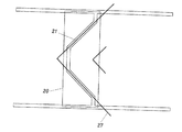
従って、本発明の第12実施例では、画素電極21の境界と画素電極に形成されている開口部27とがぶつかる部分で画素電極21の形態を変更して画素電極21の境界と開口部27とがなす角が90°以上になるようにする。これによって、図27に示されたように、画素電極21の形態は画素電極に形成された開口部27と共通電極に形成された開口部17との間で鋸の歯形に突出した形態になる。
【0128】
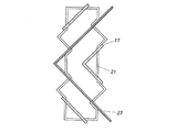
本発明の第13実施例では、画素電極の形態を開口部の形態に沿って鋸の歯形に形成する。図28は、このように画素電極を鋸の歯形に形成した本発明の第13実施例による液晶表示装置の平面図である。
【0129】
図28に示されている本発明の第13実施例による液晶表示装置のように、画素電極22を開口部17、27を囲む形態に鋸の歯形に形成すると、開口部17、27と画素電極22の境界とがぶつかる部分がなくなるので、これによるテクスチャーの問題などは発生しない。
【0130】
本発明の第12及び第13実施例における開口部の幅や間隔などは前述の実施例と類似する。
【0131】
以上では共通電極と画素電極との両方に開口パターンを形成するものについて説明したが、共通電極に開口パターンを形成する代わりに画素電極に開口パターンと共に突起を形成する方法を使用することもできる。この場合には突起はゲート絶縁膜又は保護膜などで形成する。突起を形成する時は、配線との間で寄生静電容量が形成されることに注意しなければならない。この時、開口パターン及び突起の配置は図21と同様にする。
【0132】
また、他の方法としては、画素電極には開口パターンを形成し、共通電極には突起を形成する方法がある。この場合にも開口パターン及び突起の配置は図21と同様にする。
【0133】
【発明の効果】
本発明によると、視野角が広く、液晶分子の配向が安定しており、応答速度が速い液晶表示装置を得ることができる。
【図面の簡単な説明】
【図1】従来の技術による液晶表示装置の上下電極に形成された開口パターンの重畳した状態を示す平面図である。
【図2】本発明の実施例による液晶表示装置の概略的な構造を示す断面図である。
【図3】本発明の第1及び第2実施例による液晶表示装置の上下電極に形成された開口パターンの重畳した状態を示す平面図である。
【図4】本発明の第3実施例による液晶表示装置の画素電極のパターンを示す平面図、液晶表示装置の共通電極に形成されている開口パターンを示す平面図、液晶表示装置の上下基板を整列させた状態で画素電極のパターンと共通電極の開口パターンとを重畳させた状態の平面図である。
【図5】本発明の第4実施例による液晶表示装置の画素電極のパターンを示す平面図、液晶表示装置の共通電極に形成されている開口パターンを示す平面図、液晶表示装置の上下基板を整列させた状態で画素電極のパターンと共通電極の開口パターンとを重畳させた状態の平面図である。
【図6】本発明の第5実施例による液晶表示装置の画素電極のパターンを示す平面図、液晶表示装置の共通電極に形成されている開口パターンを示す平面図、液晶表示装置の上下基板を整列させた状態で画素電極のパターンと共通電極の開口パターンとを重畳させた状態の平面図である。
【図7】本発明の第6実施例による液晶表示装置の画素電極のパターンを示す平面図、液晶表示装置の共通電極に形成されている開口パターンを示す平面図、液晶表示装置の上下基板を整列させた状態で画素電極のパターンと共通電極の開口パターンとを重畳させた状態の平面図である。
【図8】本発明の第7実施例による液晶表示装置の画素電極のパターンを示す平面図、液晶表示装置の共通電極に形成されている開口パターンを示す平面図、液晶表示装置の上下基板を整列させた状態で画素電極のパターンと共通電極の開口パターンとを重畳させた状態の平面図である。
【図9】本発明の第8実施例による液晶表示装置の画素電極のパターンを示す平面図、液晶表示装置の共通電極に形成されている開口パターンを示す平面図、液晶表示装置の上下基板を整列させた状態で画素電極のパターンと共通電極の開口パターンとを重畳させた状態の平面図である。
【図10】本発明の第9実施例による液晶表示装置の画素電極のパターンを示す平面図、液晶表示装置の共通電極に形成されている開口パターンを示す平面図、液晶表示装置の上下基板を整列させた状態で画素電極のパターンと共通電極の開口パターンとを重畳させた状態の平面図である。
【図11】パターンの幅及び間隔による応答速度及び輝度を測定するために製作したパネルの開口部パターンの多様な形態である。
【図12】各パターン別の透過率を示したグラフと、Bパターンを基準にして各パターン別の透過率の比を示したグラフである。
【図13】階調による応答時間を各パターン別に示したグラフである。
【図14】B、C、Dパターンの階調による応答時間のみを拡大して示したグラフである。
【図15】B、C、Dパターンの白色階調での顕微鏡写真である。
【図16】テストセルでのC、Dパターンの印加電圧別の顕微鏡写真である。
【図17】開口部パターンの幅が狭い場合及び広い場合のフリンジフィールドの強さを示す図面である。
【図18】開口部パターンの幅及び印加電圧によって開口部における液晶分子の配列状態を示す図面である。
【図19】図11のBパターンにおいてテクスチャーが発生する部分及びテクスチャーの発生を防止するために変更された開口部パターンを示す図面である。
【図20】図11のJパターンにおいてテクスチャーが発生する部分及びテクスチャーの発生を防止するために変更された開口部パターンを示す図面である。
【図21】図11のB、I、Jパターンにおいてテクスチャーの発生を防止するために変更された開口部パターンを示す図面である。
【図22】本発明の第10実施例による液晶表示装置の薄膜トランジスタ基板の平面図である。
【図23】本発明の第10実施例による液晶表示装置のカラーフィルタ基板の平面図である。
【図24】本発明の第10実施例による薄膜トランジスタ基板とカラーフィルタ基板とを結合した液晶表示装置の平面図である。
【図25】図24のXXV−XXV’線の断面図である。
【図26】本発明の第11実施例によるカラーフィルタ基板の平面図である。
【図27】本発明の第12実施例による液晶表示装置の平面図である。
【図28】本発明の第13実施例による液晶表示装置の平面図である。
【符号の説明】
1、2 開口パターン
3 液晶分子
10、20 基板
11 スイッチング素子
12 画素電極
14、24 偏光板
15、25 補償フィルム
21 ブラックマトリックス
22 カラーフィルタ
23 共通電極
30 液晶物質[0001]
BACKGROUND OF THE INVENTION
The present invention relates to a liquid crystal display device having a wide viewing angle, and more particularly to a liquid crystal display device of a type that widens the viewing angle by forming a certain pattern on a common electrode and a pixel electrode.
[0002]
[Prior art]
In general, a liquid crystal display device has a structure in which light transmission is adjusted by injecting liquid crystal between two substrates and adjusting the intensity of an electric field applied thereto.
[0003]
Among them, a vertically aligned (VA) type liquid crystal display device uses liquid crystal molecules aligned perpendicularly to a substrate in a state where an electric field is not applied. Light can be completely blocked in the state where no electric field is applied. That is, since the luminance in the normally black mode (off) state is very low, a high contrast ratio can be obtained as compared with the conventional twisted nematic liquid crystal display device. However, since the direction in which the liquid crystal molecules tilt is irregular when an electric field is applied, there is a portion where the polarization direction of the upper or lower polarizing plate coincides with the major axis direction of the liquid crystal molecules. Since the liquid crystal molecules do not exhibit the function of rotating the polarization direction of light, all the light is blocked by the polarizing plate. Such a portion appears black on the screen and degrades the image quality. Such a portion is called a texture.
[0004]
In order to solve such problems, various methods for patterning electrodes have been proposed. However, the conventional method of patterning the electrodes still has problems such as a slow response speed.
[0005]
Here, an electrode pattern and its problems in a conventional liquid crystal display device will be described with reference to the drawings.
[0006]
FIG. 1 is a plan view showing a state in which opening patterns formed on upper and lower electrodes of a liquid crystal display device according to the prior art are overlapped.
[0007]
The common
[0008]
At this time, when an electric field is applied between the common electrode and the pixel electrode, the
[0009]
That is, a fringe field is formed by the
[0010]
[Problems to be solved by the invention]
The slow response speed of liquid crystal molecules is a factor that induces afterimages when expressing moving images. Therefore, in order to improve the quality of moving image display, a fast response speed of liquid crystal molecules is necessary.
[0011]
The present invention is to solve the above-described problems, and an object thereof is to improve the response speed of a wide viewing angle liquid crystal display device.
[0012]
Another object of the present invention is to improve the image quality of a wide viewing angle liquid crystal display device.
[0013]
[Means for Solving the Problems]
In order to achieve the above object, in the liquid crystal display device of the present invention,Open and close the electrode openings or protrusions on the upper and lower substrates.Form as parallel as possible while adhering to the design rules.
[0014]
The following liquid crystal display is provided.
A first substrate including a pixel electrode;
A second substrate including a common electrode;
A liquid crystal display device including a liquid crystal material injected between the first substrate and the second substrate;
In a state where no voltage is applied between the pixel electrode and the common electrode, the liquid crystal molecules contained in the liquid crystal material are substantially perpendicular to both the first substrate and the second substrate. Oriented,
The pixel electrode has an opening that divides the pixel electrode region into a plurality of regions.Consist ofIncluding a first fringe field forming portion and a second fringe field forming portion;
The first fringe field forming unit is located between the first side and the second side that intersect at the first corner of the pixel electrode, from the second side toward the first side, with respect to the second side. Extending diagonally,
The second fringe field forming unit may include the second edge between the third side of the pixel electrode and the second side that intersects the second side at a second corner of the pixel electrode different from the first corner. Extending obliquely from the side toward the third side with respect to the second side,
The common electrode includes a third fringe field forming portion and a fourth fringe field forming portion including an opening or a protrusion that divides the common electrode region facing the pixel electrode into a plurality of regions,
The third fringe field forming part includes:
An area facing the area of the pixel electrode surrounded by the first side, the second side, and the first fringe field forming portion is inclined with respect to both the first side and the second side. And a first central portion extending in parallel to the first fringe field forming portion,
A first lateral end portion extending from the first central portion toward the opposite side of the first corner along the first side; and
A first vertical end extending from the first central portion toward the opposite side of the first corner along the second side;Consist of,
The fourth fringe field forming portion includes a second central portion that is inclined with respect to both the second side and the third side, and is parallel to the second fringe field forming portion.
Liquid crystal display device.
[0015]
Here, the first side is perpendicular to the second side, and the first central portion is located in the common electrode facing the second side from the region of the common electrode facing the first side. It extends to the area.
[0016]
Here, the first side is shorter than the second side, and the first central portion extends from a region of the common electrode facing the first side to a region of the common electrode facing the second side. ing.
[0017]
Here, the fourth fringe field forming portion is included in a region of the common electrode facing the region of the pixel electrode surrounded by the second side, the third side, and the second fringe field forming portion. The fourth fringe field forming portion includes a second vertical end portion extending from the second central portion toward the opposite side of the second corner along the second side.
[0018]
Here, the fourth fringe field forming portion is included in a region of the common electrode facing the region of the pixel electrode surrounded by the second side, the third side, and the second fringe field forming portion. The fourth fringe field forming portion includes a second lateral end portion extending from the second central portion toward the opposite side of the second corner along the third side.
[0019]
Here, the first fringe field forming unit, the second fringe field forming unit, the third fringe field forming unit, and the fourth fringe field forming unit are included in one pixel region, and the first fringe field forming unit is formed. And the second fringe field forming unit are separated from the first fringe field forming unit and the second fringe field forming unit included in the adjacent pixel region, or the third fringe field forming unit and the second fringe field forming unit The fourth fringe field forming part is separated from the third fringe field forming part and the fourth fringe field forming part included in the adjacent pixel region.
[0020]
Here, the third fringe field forming part and the fourth fringe field forming part are symmetric with respect to the center of the second side.
[0021]
Here, the first fringe field forming portion and the second fringe field forming portion are openings.Consist ofThe third fringe field forming portion and the fourth fringe field forming portion are protrusions.Consists of.
[0022]
Here, the common electrode has an opening or a protrusion between the third fringe field forming portion and the fourth fringe field forming portion.Consist ofA fifth fringe field forming part, the fifth fringe field forming part extending substantially parallel to the first side; and from the trunk part parallel to the first fringe field forming part. A first branch portion extending from the trunk portion; and a second branch portion extending in parallel with the second fringe field forming portion from the trunk portion.
[0023]
Here, the fifth fringe field forming portion includes a first branch extending obliquely from an end of the first branch portion along a fourth side of the pixel electrode substantially perpendicular to the first side. An end portion and a second branch end portion extending obliquely from the end of the second branch portion along the fourth side.
[0024]
Here, the fifth fringe field forming unit is included in one pixel region, and includes a third fringe field forming unit, a fourth fringe field forming unit, and a fifth fringe field forming unit included in adjacent pixel regions. It is separated.
[0030]
DETAILED DESCRIPTION OF THE INVENTION
Hereinafter, a structure of a liquid crystal display device according to an embodiment of the present invention will be described with reference to the drawings.
[0031]
FIG. 2 is a cross-sectional view showing a schematic structure of a liquid crystal display device according to an embodiment of the present invention.
[0032]
The liquid crystal display device includes a
[0033]
Pixels made of a transparent conductive material such as ITO (indium tin oxide) or IZO (indium zinc oxide) and having an opening pattern (not shown) on the
[0034]
Similar to the lower substrate, on the lower surface of the
[0035]
The polarization directions of the lower
[0036]
[0037]
Next, the opening pattern of the pixel electrode and the common electrode of the liquid crystal display device according to the embodiment of the present invention will be described with reference to the drawings.
[0038]
3A and 3B are plan views showing a state in which opening patterns formed on upper and lower electrodes of the liquid crystal display device according to the first and second embodiments of the present invention are overlapped.
[0039]
In order to improve the response speed, as shown in FIG. 3a, the opening
[0040]
However, when the opening
[0041]
In order to remedy such a problem, as shown in FIG. However, in such a form, the liquid crystal molecules cannot perform a complete one-step operation, so that a problem arises that the operation speed is slowed down again.
[0042]
Hereinafter, an opening pattern designed in consideration of both improvement of the operation speed and suppression of defects such as texture will be described.
[0043]
4a, 5a, 6a, 7a, 8a, 9a, and 10a are plan views showing pixel electrode patterns of liquid crystal display devices according to third to ninth embodiments of the present invention, respectively. , 8b, 9b, 10b are plan views showing opening patterns formed in the common electrode of the liquid crystal display device according to the third to ninth embodiments of the present invention, respectively, and FIGS. 4c, 5c, 6c, 7c, 8c, 9c and 10c are plan views showing a state in which the pixel electrode pattern and the common electrode opening pattern are superposed with the upper and lower substrates of the liquid crystal display device according to the third to ninth embodiments of the present invention aligned.
[0044]
First, a third embodiment of the present invention will be described.
As shown in FIG. 4a, a
[0045]
As shown in FIG. 4b, the
[0046]
As shown in FIG. 4c, the first to
[0047]
At this time, the upper and lower
[0048]
As a result, as shown in FIG. 4c, the number of the liquid crystal molecules rearranged by the application of the electric field lie in the polarization direction of the
[0049]
A fourth embodiment of the present invention will be described.
As shown in FIG. 5a, a first
[0050]
As shown in FIG. 5 b, the
[0051]
As shown in FIG. 5c, the first opening of the
[0052]
At this time, the upper and lower
[0053]
As a result, the same effect as in the third embodiment can be obtained.
[0054]
A fifth embodiment of the present invention will be described.
As shown in FIG. 6a, the
[0055]
As shown in FIG. 6b, the
[0056]
As shown in FIG. 6c, the third opening divides each region of the
[0057]
At this time, the upper and lower
[0058]
A sixth embodiment of the present invention will be described.
As shown in FIG. 7a, a rectangular
[0059]
As shown in FIG. 7b, X-shaped third to
[0060]
As shown in FIG. 7 c, the third to
[0061]
At this time, the upper and lower
[0062]
A seventh embodiment of the present invention will be described.
As shown in FIG. 8a, the
[0063]
As shown in FIG. 8b, the third and
[0064]
As shown in FIG. 8c, the first opening of the
[0065]
At this time, the upper and lower
[0066]
In this way, the openings are parallel to each other in most of the regions, and the direction in which the liquid crystal molecules lie laterally forms 45 ° with the polarization direction, so that it is possible to obtain a good image quality with a fast response speed and less texture. it can. The opening extends largely in two directions in the pixel region, and these two directions are 90 ° to each other. Further, since the openings of the upper and lower substrates are alternately arranged, the direction of the fringe field is classified into four directions within one pixel region.
[0067]
An eighth embodiment of the present invention will be described.
As shown in FIG. 9 a, a
[0068]
As shown in FIG. 9b, the
[0069]
As shown in FIG. 9c, the
[0070]
At this time, the upper and lower
As a result, an effect similar to that of the seventh embodiment can be obtained.
[0071]
Finally, a ninth embodiment of the present invention will be described.
As shown in FIG. 10a, the
[0072]
As shown in FIG. 10B, the
[0073]
As shown in FIG. 10 c, the
[0074]
At this time, the upper and lower
[0075]
In the above third to ninth embodiments, the opening pattern is formed so as to satisfy the conditions of the opening pattern for the divisional alignment as follows obtained as a result of various experiments. It is.
[0076]
First, in order to obtain the best viewing angle, it is preferable that a region divided into four parts is included in one pixel.
[0077]
Secondly, in order to obtain a stable divided orientation, no disclination or irregular texture should occur outside the boundaries of the divided microregions. Disclination occurs when the directors of liquid crystal molecules are arranged in various directions without being arranged in a fixed direction in a narrow region, and particularly when the liquid crystal molecules fall in a direction where they collide with each other in one region. . Therefore, in order to obtain a stable divided orientation, it is advantageous that the upper and lower substrate patterns are formed repeatedly, and the closer the ends of the upper and lower plate patterns are, the better. That is, when the liquid crystal display device is viewed from above, it is preferable that the region formed by the upper plate pattern and the lower plate pattern approximates a closed polygon. In addition, when a pattern formed on one substrate to form one region has an acute angle, disclination is likely to occur. Therefore, the pattern is preferably formed only with an obtuse angle. In addition, the stable divided orientation causes the luminance to be affected. In the disordered region, light leaks in the off state, and in the on state it becomes darker than the other surrounding parts. When the alignment of the liquid crystal molecules changes, the disordered part moves. It may cause afterimages.
[0078]
Third, in order to obtain high luminance, the following conditions must be satisfied. First, the angle formed by the liquid crystal directors in adjacent regions is most preferably 90 °. This is because disclination occurs only in the narrowest region when this occurs, and the highest luminance can be obtained when the angle formed by the transmission axis of the polarizing plate and the liquid crystal director forms 45 degrees. Moreover, it is preferable that the angle at which the opening pattern formed on each of the upper plate and the lower plate is bent or bent is as slow as possible (closer to a straight line).
[0079]
Finally, in order to obtain a fast response speed, it is preferable that the angle at which the opening pattern formed in each of the upper and lower plates bend or bend is as slow as possible (closer to a straight line). In other words, it is advantageous in terms of response speed that it is most approximate to the form of facing each other with a single letter.
[0080]
Next, the influence of the width of the opening pattern and the interval between the patterns on the transmittance and the response speed will be described.
In order to investigate the influence of the width and interval of the opening pattern, a panel having nine opening patterns shown in FIG. 11 was produced and tested.
[0081]
In FIG. 11, the pattern indicated by diagonal lines is the opening pattern of the common electrode, and the pattern indicated by thick lines is the form of the pixel electrode.
[0082]
The B, C, and D patterns and the E, F, and G patterns have the same form except for the width and interval of the patterns, respectively. The A pattern is similar to the B, C, and D patterns, but the intervals between the patterns are different. Table 1 shows the width and spacing of each pattern.
[Table 1]
FIG. 12A is a graph showing the light transmittance of a test cell for each pattern in percent (%), and FIG. 12B is a ratio of the light transmittance of other patterns based on the light transmittance of the B pattern. It is the graph which showed.
[0084]
As shown in the graphs of FIGS. 12a and 12b, the light transmittance of the G pattern is the highest at about 13%, followed by the order of the E, I, B, D, A, C, F, and J patterns. It is.
[0085]
FIG. 13 is a graph showing the response time according to the gradation of the test cell to which each pattern is applied. In actual application, only up to 64 gradations are used, but up to 110 gradations were used in this experiment.
[0086]
As shown in FIG. 13, the response times of the B, C, D, and J patterns are relatively short for all gradations. That is, the response speed was fast. The reason why the response speed is slow in the other patterns is because of the texture movement in the case of the A and I patterns, and in the case of the E, F, and G patterns, the liquid crystal molecules perform a two-stage operation.
[0087]
Table 2 shows the results obtained by applying the nine patterns of FIG. 11 to an actual panel. Experiments were made on four panels for each pattern.
[Table 2]
The actual panel results were similar to the test cell results. However, the response speed of I was relatively fast unlike the test cell, and the brightness of the J pattern was brighter than expected (in the test cell, the brightness of the J pattern was about 75% of that of the B pattern. In the panel, it was 90% compared to the B pattern).
[0089]
In the actual panel, white afterimages appeared in the A, C, I, and J patterns. A white afterimage appears strongly in the C pattern, which is problematic, but the I and J patterns can be improved to some extent.
[0090]
Based on the above results, patterns that can be selected according to the characteristics to be improved will be described.
[0091]
First, the B, D, E, and I patterns are advantageous for the purpose of improving luminance and white afterimage, and B and B for increasing the response speed while maintaining the luminance at or above the current level. The D and I patterns are preferable, and the D and J patterns are advantageous when the purpose is to improve the response speed at the expense of luminance.
[0092]
Next, in order to clarify the relationship between the response speed and the width of the opening pattern, the difference in optical characteristics will be described for B, C, and D patterns having the same form but different pattern widths.
[0093]
FIG. 14 is a graph showing response times according to the gradations of the B, C, and D patterns in an actual panel.
[0094]
The response time between 20 gradations and 40 gradations was long in the order of D <B <C. That is, the response time is shorter as the pattern width is larger.
[0095]
The response time of the C pattern is shorter than the B pattern from about 40 gradations, and the response time of the C pattern is shorter than the D pattern from about 45 gradations. However, this only appears to have a short response time due to the white afterimage phenomenon, and is not actually short. That is, the response waveform is distorted due to the white afterimage, and the response time appears to be shorter than the actual time. Therefore, in view of such points, it can be seen that the response speed increases as the pattern width increases.
[0096]
When a high voltage of 60 gradations or more is applied, the response speed is drastically slow due to texture anxiety. Among them, the D pattern having the widest width of the opening pattern has the most stable (slow increase) characteristic.
[0097]
FIG. 15 is a photomicrograph at white gradation for the C, B, and D patterns.
As shown in the photograph, the luminance of C having the lowest texture stability is the darkest, and B and D have similar brightness. Since D has a wide opening pattern width, the aperture ratio is low, but the texture stability is relatively high. It seems that the texture stability is also determined by the strength of the fringe field and the width of the pattern.
[0098]
Moreover, the form of the boundary part (part in which the opening part pattern is formed) of an area | region differs. In the case of the C pattern, the bifurcated texture appears clearly in most of the region boundary, and in the case of the B pattern, the slightly bifurcated texture appears, but in the case of the D pattern, the region boundary appears as one black line. .
[0099]
FIG. 16 is a domain division photograph according to the applied voltage of the test cell for the C pattern and the D pattern.
In the case of the C pattern, a bifurcated texture appears at the boundary of the region from 3.5 V and becomes clearer as the voltage increases. However, in the case of the D pattern, the region boundary portion is slightly divided into two branches after 5V. The reason why the region boundary is divided into two is because the liquid crystal molecules are unevenly arranged in the region. To explain this phenomenon, let us consider the strength of the fringe field according to the width of the pattern.
[0100]
FIG. 17 is a conceptual diagram showing the strength of the fringe field according to the width of the pattern.
The horizontal component of the fringe field increases as the width of the opening pattern increases. The horizontal component plays an important role in determining the direction in which the liquid crystal lies. Therefore, a wide opening pattern is effective for forming a domain. Further, the strength of the vertical component of the electric field at the center of the opening becomes weaker as the width of the opening pattern becomes wider.
[0101]
FIG. 18 is a drawing showing an alignment state of liquid crystal molecules around the opening pattern.
When the width of the opening pattern is narrow, the liquid crystal molecules lie to some extent even at the center of the opening. When the applied voltage is low, it is slightly inclined, but when the voltage is high, it lies horizontally and completely. This is because the vertical component of the electric field is strong even at the center of the opening pattern. For this reason, light leaks, and the region boundary portion is divided into bifurcated lines. Further, when the direction in which the liquid crystal molecules lie at the opening is changed by 180 °, the opening has a narrow width and thus has a strong elasticity. On the other hand, since the horizontal component of the fringe field is weak, the fringe field cannot overcome the elastic force. Therefore, the alignment of the liquid crystal molecules at the region boundary is nonuniform. Such a non-uniform arrangement of liquid crystal molecules is propagated to the inside of a small area of the pixel.
[0102]
When the width of the opening pattern is wide, the liquid crystal molecules stand vertically at the center of the opening.
As the applied voltage is increased, the liquid crystal molecules are slightly tilted, but the degree is not as great as when the width is narrow. Therefore, there is little light leaking and the small area boundary appears as one black line.
[0103]
As described above, the wider the width of the opening pattern, the faster the response speed, and the small area of the pixel is uniform. When the width of the opening pattern is wide, the aperture ratio is small, but the luminance is good because the alignment of the liquid crystal molecules becomes uniform. According to the above experiment, it is appropriate that the width of the opening pattern is about 13 ± 3 μm. At this time, the cell gap is about 4 μm to 6 μm.
[0104]
Hereinafter, the optical characteristic according to the space | interval between opening part patterns is demonstrated.
The I pattern and the J pattern have the same pattern width, and the intervals between the patterns are different from each other. In the test cell result, the I pattern and the J pattern have a remarkable difference in optical characteristics, but in the actual panel result, there is no significant difference. This is presumed to be due to a difference in the type of alignment film, a difference in the presence or absence of a protective film (insulating film), a difference in applied voltage waveform, and the like. However, when comparing the moving speed of moving images on an actual panel, the J pattern is faster than the I pattern (you can see this by drawing a black square on a gray background). However, there is a difference in response speed depending on the gradation.
[0105]
As for the width of the opening pattern, the aperture ratio is remarkably reduced when the distance between the patterns is reduced, but the luminance is not significantly different. This is for texture. That is, texture control becomes difficult when the distance between patterns becomes wide, and control becomes easy when the distance between patterns becomes narrow. Therefore, when the distance between patterns becomes narrow, the aperture ratio decreases, but the texture can be controlled appropriately, so that the luminance is compensated. However, although the I pattern has a longer distance between the patterns, the luminance is high because the texture control is relatively appropriately performed.
[0106]
In conclusion, the gradation response speed is improved as the interval between patterns is narrowed. The luminance is likely to decrease as the aperture ratio decreases, but is compensated to some extent by controlling the texture.
[0107]
Texture is closely related to response speed. Moving textures reduce response speed. When a high voltage is applied, the response speed decreases for most patterns. This is because a texture is generated. Accordingly, if the texture is appropriately controlled, not only the image quality can be improved but also the response speed can be improved. Hereinafter, a method capable of suppressing the occurrence of texture will be described.
[0108]
19 and 20 are enlarged views of portions where texture occurs in the B pattern and the J pattern, respectively.
[0109]
The opening pattern of FIG. 19 is almost similar to the pattern of FIG. 4c. However, the second and
[0110]
The portion where the texture is generated is a portion where the end portion of the opening portion of the common electrode and the end portion of the opening portion of the pixel electrode collide with each other. When the upper and lower substrates are correctly aligned, the occurrence of texture is small, but when they are misaligned, a half-moon-shaped texture is generated. The texture generated at this time does not cause a white afterimage phenomenon. As a texture suppression measure, there is a case where the width of the end of the opening of the common electrode is widened. This extends the limits of alignment errors.
[0111]
The pattern of FIG. 20 is similar to the pattern of FIG. 8c, but the number of lateral openings is different. Another difference is that the lateral opening of the pixel electrode starts from one side and a protrusion is formed at the end of the lateral opening.
[0112]
The site where the texture occurs is the end (a) of the lateral opening of the common electrode. In addition, by forming a contact hole for connection with the source electrode, texture is also generated at the lower end portion (b) of the pixel electrode having a concave shape and the end portion (c) of the vertical opening portion of the pixel electrode. To do. The texture suppression measures are as follows. In the case of part a, the width of the end of the opening of the common electrode is increased. In the case of b part, the opening part of a common electrode is made to overlap with b part. For this purpose, it is necessary to adjust the width and interval of the openings. When the interval is narrowed, the aperture ratio is reduced, but the response speed is improved. In the case of the portion c, the end of the vertical opening of the pixel electrode is formed in a sharp shape.
[0113]
A pattern to which the above texture improvement method is applied is shown in FIGS. 21 to 21c.
[0114]
On the other hand, the area where the texture is generated can be covered with the gate wiring or the black matrix.
[0115]
22 and 23 are plan views of a thin film transistor substrate and a color filter substrate of a liquid crystal display device according to a tenth embodiment of the present invention, respectively.
[0116]
As shown in FIG. 22, the
[0117]
Next, as shown in FIG. 23, on the color filter substrate, the
[0118]
24 is a plan view of a liquid crystal display device formed by joining two substrates as shown in FIGS. 22 and 23, and FIG. 25 is a cross-sectional view taken along the line XXV-XXV 'of FIG.
[0119]
24 and 25, a
[0120]
On the other hand, on the
[0121]
A liquid crystal material having a negative dielectric anisotropy is injected between the two substrates, and the liquid crystal molecules are caused by the alignment force of the
[0122]
Unlike the tenth embodiment of the present invention, the gate line is formed in the same manner as the normal method, and the portion where the opening pattern for the divisional orientation of the lower plate is formed is also covered using the black matrix. Can do. FIG. 26 is a plan view of a liquid crystal display device according to an eleventh embodiment of the present invention.
[0123]
As in the tenth embodiment of the present invention shown in FIG. 23, the
[0124]
When the black matrix is used to cover the portion where the opening is formed and the portion where the texture is generated as in the eleventh embodiment of the present invention, it is not necessary to consider the influence of the change in the gate line pattern. The luminance can be improved by widening the viewing angle of the vertical alignment liquid crystal display device with a simple process without the above process.
[0125]
In addition, the texture can be removed by changing the form of the pixel electrode instead of forming the opening.
[0126]
As described above, the portion where the texture is generated is a portion where the opening of the thin film transistor substrate and the boundary of the pixel electrode collide, but the boundary of the pixel electrode is essentially similar to the opening of the thin film transistor substrate. This is a part that violates the first condition that the angle of the bent part of the opening should be obtuse. That is, the angle formed by the opening pattern and the boundary between the pixel electrodes is an acute angle, and the alignment of the liquid crystal molecules is disturbed in this portion, resulting in a decrease in luminance, and the liquid crystal that is disturbed when the electric field applied to the liquid crystal layer changes. The arrangement of molecules moves and causes afterimages.
[0127]
Accordingly, in the twelfth embodiment of the present invention, the shape of the
[0128]
In the thirteenth embodiment of the present invention, the pixel electrode is formed in a sawtooth shape along the shape of the opening. FIG. 28 is a plan view of a liquid crystal display device according to a thirteenth embodiment of the present invention in which the pixel electrode is formed in a sawtooth shape.
[0129]
As in the liquid crystal display device according to the thirteenth embodiment of the present invention shown in FIG. 28, when the
[0130]
The widths and intervals of the openings in the twelfth and thirteenth embodiments of the present invention are similar to those of the previous embodiments.
[0131]
In the above description, the opening pattern is formed on both the common electrode and the pixel electrode. However, instead of forming the opening pattern on the common electrode, a method of forming protrusions together with the opening pattern on the pixel electrode can be used. In this case, the protrusion is formed of a gate insulating film or a protective film. When forming the protrusion, care must be taken that a parasitic capacitance is formed between the protrusion and the wiring. At this time, the opening pattern and the arrangement of the protrusions are the same as those in FIG.
[0132]
As another method, there is a method of forming an opening pattern in the pixel electrode and forming a protrusion in the common electrode. Also in this case, the arrangement of the opening pattern and the protrusions is the same as in FIG.
[0133]
【The invention's effect】
According to the present invention, a liquid crystal display device having a wide viewing angle, stable alignment of liquid crystal molecules, and a high response speed can be obtained.
[Brief description of the drawings]
FIG. 1 is a plan view showing a state in which aperture patterns formed on upper and lower electrodes of a liquid crystal display device according to a conventional technique are superimposed.
FIG. 2 is a cross-sectional view showing a schematic structure of a liquid crystal display device according to an embodiment of the present invention.
FIG. 3 is a plan view illustrating a state in which opening patterns formed on upper and lower electrodes of a liquid crystal display device according to first and second embodiments of the present invention are overlapped.
FIG. 4 is a plan view showing a pattern of pixel electrodes of a liquid crystal display device according to a third embodiment of the present invention, a plan view showing an opening pattern formed in a common electrode of the liquid crystal display device, and upper and lower substrates of the liquid crystal display device. It is a top view of the state which overlapped the pattern of the pixel electrode and the opening pattern of the common electrode in the aligned state.
FIG. 5 is a plan view showing a pixel electrode pattern of a liquid crystal display device according to a fourth embodiment of the present invention, a plan view showing an opening pattern formed in a common electrode of the liquid crystal display device, and upper and lower substrates of the liquid crystal display device. It is a top view of the state which overlapped the pattern of the pixel electrode and the opening pattern of the common electrode in the aligned state.
FIG. 6 is a plan view showing pixel electrode patterns of a liquid crystal display device according to a fifth embodiment of the present invention, a plan view showing opening patterns formed in a common electrode of the liquid crystal display device, and upper and lower substrates of the liquid crystal display device. It is a top view of the state which overlapped the pattern of the pixel electrode and the opening pattern of the common electrode in the aligned state.
FIG. 7 is a plan view showing pixel electrode patterns of a liquid crystal display device according to a sixth embodiment of the present invention, a plan view showing opening patterns formed in a common electrode of the liquid crystal display device, and upper and lower substrates of the liquid crystal display device. It is a top view of the state which overlapped the pattern of the pixel electrode and the opening pattern of the common electrode in the aligned state.
FIG. 8 is a plan view showing a pattern of pixel electrodes of a liquid crystal display device according to a seventh embodiment of the present invention, a plan view showing an opening pattern formed in a common electrode of the liquid crystal display device, and upper and lower substrates of the liquid crystal display device. It is a top view of the state which overlapped the pattern of the pixel electrode and the opening pattern of the common electrode in the aligned state.
FIG. 9 is a plan view showing a pattern of pixel electrodes of a liquid crystal display device according to an eighth embodiment of the present invention, a plan view showing an opening pattern formed in a common electrode of the liquid crystal display device, and upper and lower substrates of the liquid crystal display device. It is a top view of the state which overlapped the pattern of the pixel electrode and the opening pattern of the common electrode in the aligned state.
FIG. 10 is a plan view showing a pattern of pixel electrodes of a liquid crystal display device according to a ninth embodiment of the present invention, a plan view showing an opening pattern formed in a common electrode of the liquid crystal display device, and upper and lower substrates of the liquid crystal display device. It is a top view of the state which overlapped the pattern of the pixel electrode and the opening pattern of the common electrode in the aligned state.
FIGS. 11A and 11B are various shapes of an opening pattern of a panel manufactured to measure response speed and brightness according to a pattern width and interval. FIGS.
FIG. 12 is a graph showing the transmittance for each pattern and a graph showing the ratio of the transmittance for each pattern with reference to the B pattern.
FIG. 13 is a graph showing the response time by gradation for each pattern.
FIG. 14 is a graph showing an enlarged response time based on gradations of B, C, and D patterns only.
FIG. 15 is a photomicrograph at white gradation of B, C, and D patterns.
FIG. 16 is a photomicrograph according to applied voltage of C and D patterns in a test cell.
FIG. 17 is a diagram showing the strength of the fringe field when the width of the opening pattern is narrow and wide.
FIG. 18 is a diagram illustrating an alignment state of liquid crystal molecules in the opening according to the width of the opening pattern and the applied voltage.
19 is a diagram showing a portion where a texture is generated in the B pattern of FIG. 11 and an opening pattern changed to prevent the generation of the texture.
20 is a diagram illustrating a portion where a texture is generated in the J pattern of FIG. 11 and an opening portion pattern changed to prevent the generation of the texture.
FIG. 21 is a diagram illustrating an opening pattern that has been changed in order to prevent the occurrence of texture in the B, I, and J patterns of FIG. 11;
FIG. 22 is a plan view of a thin film transistor substrate of a liquid crystal display device according to a tenth embodiment of the present invention.
FIG. 23 is a plan view of a color filter substrate of a liquid crystal display device according to a tenth embodiment of the present invention.
FIG. 24 is a plan view of a liquid crystal display device in which a thin film transistor substrate and a color filter substrate are combined according to a tenth embodiment of the present invention.
25 is a sectional view taken along line XXV-XXV ′ in FIG. 24. FIG.
FIG. 26 is a plan view of a color filter substrate according to an eleventh embodiment of the present invention.
FIG. 27 is a plan view of a liquid crystal display device according to a twelfth embodiment of the present invention.
FIG. 28 is a plan view of a liquid crystal display device according to a thirteenth embodiment of the present invention.
[Explanation of symbols]
1, 2 Opening pattern
3 Liquid crystal molecules
10, 20 substrate
11 Switching element
12 pixel electrodes
14, 24 Polarizing plate
15, 25 Compensation film
21 Black Matrix
22 Color filter
23 Common electrode
30 Liquid crystal substances
Claims (11)
共通電極を含む第2基板と、
前記第1基板と前記第2基板との間に注入されている液晶物質とを含む液晶表示装置であり、
前記画素電極と前記共通電極との間に電圧が印加されていない状態では、前記液晶物質に含まれる液晶分子は前記第1基板と前記第2基板とのいずれに対しても実質的に垂直に配向され、
前記画素電極は、前記画素電極の領域を複数に区切る開口部からなる第1フリンジフィールド形成部と第2フリンジフィールド形成部とを含み、
前記第1フリンジフィールド形成部は、前記画素電極の第1角で交わる第1辺と第2辺との間で、前記第2辺から前記第1辺に向かって、前記第2辺に対して斜めに延び、
前記第2フリンジフィールド形成部は、前記第1角とは異なる前記画素電極の第2角で前記第2辺と交わる前記画素電極の第3辺と前記第2辺との間で、前記第2辺から前記第3辺に向かって、前記第2辺に対して斜めに延び、
前記共通電極は、前記画素電極と対向する前記共通電極の領域を複数に区切る開口部又は突起を含む第3フリンジフィールド形成部と第4フリンジフィールド形成部とを含み、
前記第3フリンジフィールド形成部は、
前記第1辺、前記第2辺、及び前記第1フリンジフィールド形成部で囲まれた前記画素電極の領域に対向する領域を、前記第1辺と前記第2辺との両方に対しては斜めに、前記第1フリンジフィールド形成部に対しては平行に延びている第1中央部、
前記第1辺に沿って前記第1中央部から前記第1角とは反対側に向かって延びている第1横端部、及び、
前記第2辺に沿って前記第1中央部から前記第1角とは反対側に向かって延びている第1縦端部、からなり、
前記第4フリンジフィールド形成部は、前記第2辺と前記第3辺との両方に対しては斜めであり、前記第2フリンジフィールド形成部に対しては平行である第2中央部を含む、
液晶表示装置。A first substrate including a pixel electrode;
A second substrate including a common electrode;
A liquid crystal display device comprising a liquid crystal material injected between the first substrate and the second substrate;
In a state where no voltage is applied between the pixel electrode and the common electrode, the liquid crystal molecules contained in the liquid crystal material are substantially perpendicular to both the first substrate and the second substrate. Oriented,
The pixel electrode includes a first fringe field forming portion consisting of the openings delimiting the area of the pixel electrode into a plurality and the second fringe field forming unit,
The first fringe field forming unit is located between the first side and the second side that intersect at the first corner of the pixel electrode, from the second side toward the first side, with respect to the second side. Extending diagonally,
The second fringe field forming unit may include the second edge between the third side of the pixel electrode and the second side that intersects the second side at a second corner of the pixel electrode different from the first corner. Extending obliquely from the side toward the third side with respect to the second side,
The common electrode includes a third fringe field forming portion and a fourth fringe field forming portion including an opening or a protrusion that divides the common electrode region facing the pixel electrode into a plurality of regions,
The third fringe field forming part includes:
An area facing the area of the pixel electrode surrounded by the first side, the second side, and the first fringe field forming portion is inclined with respect to both the first side and the second side. And a first central portion extending in parallel to the first fringe field forming portion,
A first lateral end portion extending from the first central portion toward the opposite side of the first corner along the first side; and
First Tatetan portion extending toward the opposite side of the first angle from said first central portion along the second side, consists,
The fourth fringe field forming portion includes a second central portion that is inclined with respect to both the second side and the third side, and is parallel to the second fringe field forming portion.
Liquid crystal display device.
前記第4フリンジフィールド形成部は、前記第2辺に沿って前記第2中央部から前記第2角とは反対側に向かって延びている第2縦端部を含む、
請求項1に記載の液晶表示装置。The fourth fringe field forming part is included in the common electrode region facing the pixel electrode region surrounded by the second side, the third side, and the second fringe field forming unit,
The fourth fringe field forming portion includes a second vertical end portion extending from the second central portion toward the opposite side of the second corner along the second side.
The liquid crystal display device according to claim 1.
前記第4フリンジフィールド形成部は、前記第3辺に沿って前記第2中央部から前記第2角とは反対側に向かって延びている第2横端部を含む、
請求項1に記載の液晶表示装置。The fourth fringe field forming part is included in the common electrode region facing the pixel electrode region surrounded by the second side, the third side, and the second fringe field forming unit,
The fourth fringe field forming portion includes a second lateral end portion extending from the second central portion toward the opposite side of the second corner along the third side.
The liquid crystal display device according to claim 1.
前記第5フリンジフィールド形成部は、
前記第1辺に対して実質的に平行に延びている幹部、
前記幹部から前記第1フリンジフィールド形成部に対して平行に延びている第1枝部、及び、
前記幹部から前記第2フリンジフィールド形成部に対して平行に延びている第2枝部、
を含む、請求項1に記載の液晶表示装置。The common electrode includes a fifth fringe field forming portion consisting of the openings or protrusions between the third fringe field forming unit and the fourth fringe field forming unit,
The fifth fringe field forming portion includes:
A trunk extending substantially parallel to the first side;
A first branch extending parallel to the first fringe field forming portion from the trunk, and
A second branch extending parallel to the second fringe field forming part from the trunk part;
The liquid crystal display device according to claim 1, comprising:
前記第1辺に対して実質的に垂直な前記画素電極の第4辺に沿って前記第1枝部の端から斜めに延びている第1枝端部と、
前記第4辺に沿って前記第2枝部の端から斜めに延びている第2枝端部と、
を含む、請求項9に記載の液晶表示装置。The fifth fringe field forming portion includes:
A first branch end extending obliquely from an end of the first branch along a fourth side of the pixel electrode substantially perpendicular to the first side;
A second branch end extending obliquely from the end of the second branch along the fourth side;
The liquid crystal display device according to claim 9, comprising:
Applications Claiming Priority (2)
| Application Number | Priority Date | Filing Date | Title |
|---|---|---|---|
| KR1019990042216A KR100354906B1 (en) | 1999-10-01 | 1999-10-01 | A wide viewing angle liquid crystal display |
| KR1999P42216 | 1999-10-01 |
Related Child Applications (1)
| Application Number | Title | Priority Date | Filing Date |
|---|---|---|---|
| JP2008314954A Division JP5232959B2 (en) | 1999-10-01 | 2008-12-10 | Wide viewing angle LCD |
Publications (3)
| Publication Number | Publication Date |
|---|---|
| JP2001109009A JP2001109009A (en) | 2001-04-20 |
| JP2001109009A5 JP2001109009A5 (en) | 2008-03-06 |
| JP4550191B2 true JP4550191B2 (en) | 2010-09-22 |
Family
ID=19613553
Family Applications (2)
| Application Number | Title | Priority Date | Filing Date |
|---|---|---|---|
| JP33059599A Expired - Fee Related JP4550191B2 (en) | 1999-10-01 | 1999-11-19 | Wide viewing angle LCD |
| JP2008314954A Expired - Fee Related JP5232959B2 (en) | 1999-10-01 | 2008-12-10 | Wide viewing angle LCD |
Family Applications After (1)
| Application Number | Title | Priority Date | Filing Date |
|---|---|---|---|
| JP2008314954A Expired - Fee Related JP5232959B2 (en) | 1999-10-01 | 2008-12-10 | Wide viewing angle LCD |
Country Status (6)
| Country | Link |
|---|---|
| US (9) | US6738120B1 (en) |
| EP (5) | EP2320264B1 (en) |
| JP (2) | JP4550191B2 (en) |
| KR (1) | KR100354906B1 (en) |
| CN (3) | CN1198170C (en) |
| TW (1) | TW525031B (en) |
Families Citing this family (112)
| Publication number | Priority date | Publication date | Assignee | Title |
|---|---|---|---|---|
| KR100309918B1 (en) * | 1998-05-16 | 2001-12-17 | 윤종용 | Liquid crystal display having wide viewing angle and method for manufacturing the same |
| KR100354906B1 (en) * | 1999-10-01 | 2002-09-30 | 삼성전자 주식회사 | A wide viewing angle liquid crystal display |
| KR100635940B1 (en) * | 1999-10-29 | 2006-10-18 | 삼성전자주식회사 | A vertically aligned mode liquid crystal display |
| KR100345961B1 (en) * | 2001-01-12 | 2002-08-01 | Samsung Electronics Co Ltd | Liquid crystal display with wide viewing angle |
| TW575774B (en) * | 2000-09-05 | 2004-02-11 | Sanyo Electric Co | Liquid crystal display device |
| US7408605B2 (en) * | 2000-09-19 | 2008-08-05 | Samsung Electronics Co., Ltd. | Liquid crystal display panel |
| US6812911B2 (en) * | 2000-12-04 | 2004-11-02 | Hitachi, Ltd. | Liquid crystal display device |
| JP5041629B2 (en) * | 2001-06-06 | 2012-10-03 | 奇美電子股▲ふん▼有限公司 | Liquid crystal display |
| KR20030004458A (en) | 2001-07-05 | 2003-01-15 | 삼성전자 주식회사 | a vertically aligned mode liquid crystal display |
| JP2003029283A (en) * | 2001-07-17 | 2003-01-29 | Toshiba Corp | Liquid crystal display device |
| KR20030042221A (en) * | 2001-11-22 | 2003-05-28 | 삼성전자주식회사 | a thin film transistor array panel for a liquid crystal display |
| KR100859508B1 (en) * | 2001-12-07 | 2008-09-22 | 삼성전자주식회사 | a liquid crystal display |
| KR100831229B1 (en) * | 2001-12-10 | 2008-05-22 | 삼성전자주식회사 | A liquid crystal display having high aperture ratio |
| KR100752213B1 (en) * | 2001-12-20 | 2007-08-28 | 엘지.필립스 엘시디 주식회사 | Liquid Crystal Display Device |
| JP3778185B2 (en) | 2002-11-08 | 2006-05-24 | セイコーエプソン株式会社 | Liquid crystal display device and electronic device |
| KR100925459B1 (en) * | 2002-12-24 | 2009-11-06 | 삼성전자주식회사 | Liquid crystal display having multi domain and panel for the same |
| KR100929675B1 (en) * | 2003-03-24 | 2009-12-03 | 삼성전자주식회사 | Multi-domain liquid crystal display device and thin film transistor substrate thereof |
| KR100961945B1 (en) | 2003-03-26 | 2010-06-08 | 삼성전자주식회사 | Liquid crystal display and panel for the same |
| KR100920355B1 (en) * | 2003-03-28 | 2009-10-07 | 삼성전자주식회사 | thin film diode panel for liquid crystal display and liquid crystal display including the panel |
| KR100951348B1 (en) | 2003-04-04 | 2010-04-08 | 삼성전자주식회사 | Multi-domain liquid crystal display and a thin film transistor substrate of the same |
| KR20040089141A (en) * | 2003-04-10 | 2004-10-21 | 삼성전자주식회사 | Liquid crystal display |
| KR100961946B1 (en) * | 2003-05-13 | 2010-06-10 | 삼성전자주식회사 | A vertically aligned mode liquid crystal display |
| KR100984346B1 (en) * | 2003-05-19 | 2010-09-30 | 삼성전자주식회사 | Liquid crystal display having multi domain and panel for the same |
| KR20040105934A (en) | 2003-06-10 | 2004-12-17 | 삼성전자주식회사 | Liquid crystal display having multi domain and panel for the same |
| JP4880208B2 (en) * | 2003-07-02 | 2012-02-22 | 三星電子株式会社 | Display panel and multi-domain liquid crystal display device including the same |
| KR100980016B1 (en) * | 2003-08-04 | 2010-09-03 | 삼성전자주식회사 | Thin film transistor array panel |
| KR101337260B1 (en) * | 2003-08-13 | 2013-12-05 | 삼성디스플레이 주식회사 | Multi-domain liquid crystal display and a thin film transistor substrate of the same |
| KR20050036128A (en) * | 2003-10-15 | 2005-04-20 | 삼성전자주식회사 | Multi-domain liquid crystal display including the same |
| US8098355B2 (en) | 2003-10-15 | 2012-01-17 | Samsung Electronics Co., Ltd. | Liquid crystal display |
| KR20050063016A (en) | 2003-12-19 | 2005-06-28 | 삼성전자주식회사 | Multi-domain thin film transistor array panel and liquid crystal display including the same |
| KR101189267B1 (en) * | 2004-12-03 | 2012-10-09 | 삼성디스플레이 주식회사 | A thin film transistor array panel and a liquid crystal display |
| JP2005309290A (en) | 2004-04-26 | 2005-11-04 | Sumitomo Chemical Co Ltd | Combined polarizer, its manufacturing method and liquid crystal display device |
| US7573551B2 (en) * | 2004-05-21 | 2009-08-11 | Sanyo Electric Co., Ltd. | Transflective liquid crystal display device and color liquid crystal display device |
| JP2005338215A (en) * | 2004-05-25 | 2005-12-08 | Sumitomo Chemical Co Ltd | Composite retardation film and method for manufacturing composite optical member |
| JP4543776B2 (en) * | 2004-06-24 | 2010-09-15 | 住友化学株式会社 | Retardation plate and composite polarizing plate, manufacturing method thereof, and liquid crystal display device |
| JP4844027B2 (en) * | 2004-07-16 | 2011-12-21 | カシオ計算機株式会社 | Vertical alignment type liquid crystal display element |
| US7221413B2 (en) * | 2004-08-05 | 2007-05-22 | Au Optronics Corporation | Thin film transistor array substrate and repairing method thereof |
| KR101160825B1 (en) * | 2004-08-18 | 2012-06-29 | 삼성전자주식회사 | Liquid crystal display |
| CN100476554C (en) * | 2004-08-31 | 2009-04-08 | 卡西欧计算机株式会社 | Vertical alignment active matrix liquid crystal display device |
| KR101061848B1 (en) | 2004-09-09 | 2011-09-02 | 삼성전자주식회사 | Thin film transistor panel and multi-domain liquid crystal display including the same |
| CN100492141C (en) * | 2004-09-30 | 2009-05-27 | 卡西欧计算机株式会社 | Vertical alignment active matrix liquid crystal display device |
| US20060066791A1 (en) * | 2004-09-30 | 2006-03-30 | Casio Computer Co., Ltd. | Vertical alignment active matrix liquid crystal display device |
| KR101133757B1 (en) * | 2004-11-25 | 2012-04-09 | 삼성전자주식회사 | Liquid crystal display |
| TWI290649B (en) * | 2004-11-29 | 2007-12-01 | Casio Computer Co Ltd | Vertical alignment active matrix liquid crystal display device |
| KR100752876B1 (en) * | 2004-11-30 | 2007-08-29 | 가시오게산키 가부시키가이샤 | Vertical-alignment liquid crystal display device |
| US8068200B2 (en) * | 2004-12-24 | 2011-11-29 | Casio Computer Co., Ltd. | Vertical alignment liquid crystal display device in which a pixel electrode has slits which divide the pixel electrode into electrode portions |
| JP4752266B2 (en) * | 2004-12-24 | 2011-08-17 | カシオ計算機株式会社 | Liquid crystal display element |
| JP4639797B2 (en) * | 2004-12-24 | 2011-02-23 | カシオ計算機株式会社 | Liquid crystal display element |
| US7639333B2 (en) * | 2005-04-06 | 2009-12-29 | Samsung Electronics Co., Ltd. | Display panel and liquid crystal display apparatus including the same |
| KR101189270B1 (en) * | 2005-04-06 | 2012-10-15 | 삼성디스플레이 주식회사 | Panel and liquid crystal display includig the same |
| CN100361014C (en) * | 2005-05-23 | 2008-01-09 | 友达光电股份有限公司 | Liquid crystal display panel, active element array substrate and its mfg. method |
| WO2006126405A1 (en) * | 2005-05-25 | 2006-11-30 | Sharp Kabushiki Kaisha | Liquid crystal display device substrate, liquid crystal display device substrate manufacturing method, liquid crystal display device, and liquid crystal display device manufacturing method |
| JP4640025B2 (en) * | 2005-06-24 | 2011-03-02 | 住友化学株式会社 | Coating liquid for coating phase difference plate, method for producing phase difference plate using the same, and method for producing composite polarizing plate |
| KR101171180B1 (en) * | 2005-07-15 | 2012-08-20 | 삼성전자주식회사 | Liquid crystal display |
| KR101153942B1 (en) * | 2005-07-20 | 2012-06-08 | 삼성전자주식회사 | Liquid crystal display |
| KR100984434B1 (en) * | 2005-09-30 | 2010-09-30 | 샤프 가부시키가이샤 | Liquid crystal display and method for manufacturing same |
| JP5080978B2 (en) | 2005-09-30 | 2012-11-21 | シャープ株式会社 | Method for manufacturing thin film transistor array substrate |
| KR101224047B1 (en) * | 2005-12-30 | 2013-01-18 | 엘지디스플레이 주식회사 | In plane switching mode liquid crystal display device |
| KR20070087395A (en) * | 2006-02-23 | 2007-08-28 | 삼성전자주식회사 | Display panel |
| JP4846401B2 (en) * | 2006-03-17 | 2011-12-28 | スタンレー電気株式会社 | Liquid crystal display element |
| TWI330274B (en) * | 2006-03-22 | 2010-09-11 | Chi Mei Optoelectronics Corp | Multi-domain vertically alignment liquid crystal display panel |
| US20070229744A1 (en) * | 2006-03-29 | 2007-10-04 | Casio Computer Co., Ltd. | Vertically aligned liquid crystal display device |
| US20090290104A1 (en) * | 2006-07-18 | 2009-11-26 | Sumitomo Chemical Company, Limited | Composite polarizing plate, method for producing the same, composite optical member and liquid crystal display |
| KR20080010159A (en) | 2006-07-26 | 2008-01-30 | 삼성전자주식회사 | Liquid crystal display |
| JP4203676B2 (en) * | 2006-09-27 | 2009-01-07 | カシオ計算機株式会社 | Liquid crystal display element |
| US8174655B2 (en) * | 2006-12-22 | 2012-05-08 | Lg Display Co., Ltd. | Liquid crystal display device and method of fabricating the same |
| KR20080087525A (en) * | 2007-03-27 | 2008-10-01 | 삼성전자주식회사 | Liquid crystal display device and driving method of the same |
| KR101329779B1 (en) * | 2007-04-12 | 2013-11-15 | 삼성디스플레이 주식회사 | Display substrate, method of manufacturing thereof and display apparatus having the same |
| JP4571166B2 (en) * | 2007-05-18 | 2010-10-27 | 統寶光電股▲ふん▼有限公司 | Vertical alignment type liquid crystal display device |
| JP4613935B2 (en) * | 2007-07-19 | 2011-01-19 | ソニー株式会社 | Liquid crystal display device |
| JP4556988B2 (en) * | 2007-11-16 | 2010-10-06 | セイコーエプソン株式会社 | Liquid crystal display device and electronic device |
| JP4783798B2 (en) * | 2008-01-15 | 2011-09-28 | シャープ株式会社 | Liquid crystal display device and manufacturing method thereof |
| KR20090084176A (en) * | 2008-01-31 | 2009-08-05 | 삼성전자주식회사 | Liquid crystal display |
| JP5228562B2 (en) * | 2008-03-25 | 2013-07-03 | 株式会社ニコン | Liquid crystal panel, display device and projector |
| KR101494316B1 (en) * | 2008-07-14 | 2015-02-23 | 삼성디스플레이 주식회사 | Display panel and method for manufacturing the display panel |
| JP5036678B2 (en) * | 2008-10-06 | 2012-09-26 | シャープ株式会社 | Liquid crystal display |
| KR101006454B1 (en) * | 2009-12-28 | 2011-01-06 | 삼성전자주식회사 | Thin film transistor array panel |
| KR101232181B1 (en) * | 2010-02-03 | 2013-02-12 | 엘지디스플레이 주식회사 | Mask Assembly |
| US7999899B1 (en) | 2011-01-25 | 2011-08-16 | Hannstar Display Corp. | Fringe field switching liquid crystal display apparatus |
| JP2012198443A (en) * | 2011-03-23 | 2012-10-18 | Sony Corp | Liquid crystal display, and method for manufacturing the same |
| KR20120122763A (en) * | 2011-04-29 | 2012-11-07 | 삼성디스플레이 주식회사 | Image display apparatus |
| KR20120124012A (en) | 2011-05-02 | 2012-11-12 | 삼성디스플레이 주식회사 | Liquid crystal display |
| KR20120124011A (en) * | 2011-05-02 | 2012-11-12 | 삼성디스플레이 주식회사 | Liquid crystal display |
| US8189158B1 (en) | 2011-09-29 | 2012-05-29 | Hannstar Display Corp. | Fringe field switching liquid crystal display apparatus |
| JP2012108553A (en) * | 2012-02-28 | 2012-06-07 | Japan Display East Co Ltd | Liquid crystal display device |
| KR20130139548A (en) * | 2012-06-13 | 2013-12-23 | 삼성디스플레이 주식회사 | Liquid crystal display |
| JP5963564B2 (en) * | 2012-06-20 | 2016-08-03 | スタンレー電気株式会社 | Liquid crystal display |
| CN104520762B (en) * | 2012-06-25 | 2018-02-16 | 汉阳大学校产学协力团 | The method of liquid crystal display device and driving liquid crystal display device |
| KR20140001071A (en) | 2012-06-25 | 2014-01-06 | 한양대학교 산학협력단 | Liquid crystal compound |
| WO2015008696A1 (en) * | 2013-07-19 | 2015-01-22 | 堺ディスプレイプロダクト株式会社 | Display panel and display device |
| TWI512378B (en) * | 2013-08-19 | 2015-12-11 | Au Optronics Corp | Pixel structure |
| KR102117397B1 (en) * | 2013-10-08 | 2020-06-02 | 삼성디스플레이 주식회사 | Display apparatus |
| KR102114153B1 (en) | 2013-11-13 | 2020-05-25 | 삼성디스플레이 주식회사 | Liquid crystal display |
| CN103943629B (en) * | 2013-12-23 | 2016-09-14 | 厦门天马微电子有限公司 | Tft array substrate, display floater and display device |
| TWI476493B (en) * | 2014-02-14 | 2015-03-11 | Au Optronics Corp | Pixel structure |
| KR102204058B1 (en) * | 2014-02-14 | 2021-01-19 | 삼성디스플레이 주식회사 | Curved Display Apparatus |
| KR102233518B1 (en) | 2014-09-11 | 2021-03-30 | 삼성디스플레이 주식회사 | Display device |
| JP6430299B2 (en) * | 2015-03-11 | 2018-11-28 | スタンレー電気株式会社 | Liquid crystal display |
| KR102389875B1 (en) * | 2015-09-01 | 2022-04-22 | 삼성디스플레이 주식회사 | Liquid crystal display device |
| US10490122B2 (en) | 2016-02-29 | 2019-11-26 | Samsung Display Co., Ltd. | Display device |
| KR102480893B1 (en) * | 2016-04-04 | 2022-12-26 | 삼성디스플레이 주식회사 | Display substrate and liquid crystal display comprising the same |
| KR102491239B1 (en) * | 2016-05-03 | 2023-01-25 | 삼성디스플레이 주식회사 | Liquid crystal display device |
| KR102605283B1 (en) | 2016-06-30 | 2023-11-27 | 삼성디스플레이 주식회사 | Display device |
| KR102613863B1 (en) * | 2016-09-22 | 2023-12-18 | 삼성디스플레이 주식회사 | Display device |
| KR102611958B1 (en) | 2016-09-23 | 2023-12-12 | 삼성디스플레이 주식회사 | Display device |
| KR102559096B1 (en) | 2016-11-29 | 2023-07-26 | 삼성디스플레이 주식회사 | Display device |
| KR20180061568A (en) | 2016-11-29 | 2018-06-08 | 삼성디스플레이 주식회사 | Display device |
| KR20180096875A (en) | 2017-02-21 | 2018-08-30 | 삼성디스플레이 주식회사 | Display device |
| KR102417989B1 (en) | 2017-05-23 | 2022-07-07 | 삼성디스플레이 주식회사 | Display device |
| KR102394406B1 (en) * | 2017-12-05 | 2022-05-03 | 엘지디스플레이 주식회사 | Liquid Crystal Display |
| TWI683161B (en) | 2018-08-07 | 2020-01-21 | 友達光電股份有限公司 | Pixel structure |
| KR20210105236A (en) | 2020-02-18 | 2021-08-26 | 삼성전자주식회사 | Display apparatus and control method thereof |
Family Cites Families (110)
| Publication number | Priority date | Publication date | Assignee | Title |
|---|---|---|---|---|
| GB1462978A (en) | 1974-04-17 | 1977-01-26 | Rank Organisation Ltd | Optical apparatus |
| US4385806A (en) * | 1978-06-08 | 1983-05-31 | Fergason James L | Liquid crystal display with improved angle of view and response times |
| JPH0829790B2 (en) | 1984-03-14 | 1996-03-27 | カルマー・インコーポレーテッド | Viscous product dispenser with externally located outlet valve with idle motion to cut dispensed product |
| FR2564605B1 (en) | 1984-05-18 | 1987-12-24 | Commissariat Energie Atomique | LIQUID CRYSTAL CELL CAPABLE OF PRESENTING A HOMEOTROPIC STRUCTURE, WITH BIREFRINGENCE COMPENSATED FOR THIS STRUCTURE |
| FR2568393B1 (en) * | 1984-07-26 | 1986-11-14 | Commissariat Energie Atomique | AN ELECTRICALLY CONTROLLED BIREFRINGENCE TYPE NEMATIC LIQUID CRYSTAL LOW DOPED BY A CHIRAL SOLUTE |
| FR2595156B1 (en) * | 1986-02-28 | 1988-04-29 | Commissariat Energie Atomique | LIQUID CRYSTAL CELL USING ELECTRICALLY CONTROLLED BIREFRINGENCE EFFECT AND METHODS OF MANUFACTURING THE CELL AND A UNIAXIC NEGATIVE ANISOTROPY ANISOTROPY MEDIUM FOR USE THEREIN |
| US4878742A (en) | 1986-08-04 | 1989-11-07 | Canon Kabushiki Kaisha | Liquid crystal optical modulator |
| US5172256A (en) | 1988-01-19 | 1992-12-15 | Sethofer Nicholas L | Liquid crystal variable color density lens and eye protective devices incorporating the same |
| JPH01189629A (en) | 1988-01-26 | 1989-07-28 | Seiko Instr & Electron Ltd | Liquid crystal display device and its production |
| JPH01196020A (en) | 1988-02-01 | 1989-08-07 | Bio Toron:Kk | Liquid crystal cell having plastic film substrate and surface cleaning method for plastic film substrate for said liquid crystal cell and surface treatment thereof |
| JPH0235416A (en) | 1988-07-26 | 1990-02-06 | Toshiba Corp | Liquid crystal display device |
| JPH02151830A (en) | 1988-12-05 | 1990-06-11 | Seiko Epson Corp | Liquid crystal electrooptic element |
| JPH02190825A (en) | 1989-01-20 | 1990-07-26 | Seiko Epson Corp | Liquid crystal electro-optical element |
| JPH0754363B2 (en) | 1989-07-11 | 1995-06-07 | 凸版印刷株式会社 | Color filter peeling method |
| JPH03209220A (en) | 1990-01-11 | 1991-09-12 | Matsushita Electric Ind Co Ltd | Production of optical modulating element |
| JP2507122B2 (en) | 1990-03-08 | 1996-06-12 | スタンレー電気株式会社 | Liquid crystal display |
| JPH03261914A (en) | 1990-03-13 | 1991-11-21 | Asahi Glass Co Ltd | Liquid crystal display element |
| JPH0829812B2 (en) | 1990-06-14 | 1996-03-27 | 株式会社日本システムアカデミー | Product sorting method |
| JPH07104450B2 (en) * | 1990-10-17 | 1995-11-13 | スタンレー電気株式会社 | Biaxial optical element and manufacturing method thereof |
| JP3047477B2 (en) | 1991-01-09 | 2000-05-29 | 松下電器産業株式会社 | Liquid crystal display device and projection display device using the same |
| US5473455A (en) * | 1991-12-20 | 1995-12-05 | Fujitsu Limited | Domain divided liquid crystal display device with particular pretilt angles and directions in each domain |
| JP3087193B2 (en) | 1991-12-20 | 2000-09-11 | 富士通株式会社 | Liquid crystal display |
| JPH0815714B2 (en) | 1992-01-07 | 1996-02-21 | 株式会社川上製作所 | Laminate cutting device |
| US5473450A (en) | 1992-04-28 | 1995-12-05 | Sharp Kabushiki Kaisha | Liquid crystal display device with a polymer between liquid crystal regions |
| US5309264A (en) * | 1992-04-30 | 1994-05-03 | International Business Machines Corporation | Liquid crystal displays having multi-domain cells |
| JP3206133B2 (en) | 1992-09-07 | 2001-09-04 | 住友化学工業株式会社 | Liquid crystal display |
| KR950003877B1 (en) * | 1992-09-17 | 1995-04-20 | 삼성전자 주식회사 | Cache updating device and method |
| KR960001941B1 (en) * | 1992-11-10 | 1996-02-08 | 재단법인한국전자통신연구소 | Plate display device |
| JP2921813B2 (en) | 1993-03-04 | 1999-07-19 | シャープ株式会社 | Electrode structure of liquid crystal display |
| JPH06301036A (en) * | 1993-04-12 | 1994-10-28 | Sanyo Electric Co Ltd | Liquid crystal display device |
| US5579140A (en) * | 1993-04-22 | 1996-11-26 | Sharp Kabushiki Kaisha | Multiple domain liquid crystal display element and a manufacturing method of the same |
| JP2975844B2 (en) | 1993-06-24 | 1999-11-10 | 三洋電機株式会社 | Liquid crystal display |
| JP2859093B2 (en) | 1993-06-28 | 1999-02-17 | 三洋電機株式会社 | Liquid crystal display |
| JPH0720469A (en) | 1993-06-29 | 1995-01-24 | Tokuo Koma | Liquid crystal display device |
| JP3234357B2 (en) | 1993-07-08 | 2001-12-04 | 三洋電機株式会社 | Liquid crystal display |
| JP3164702B2 (en) | 1993-07-27 | 2001-05-08 | シャープ株式会社 | Liquid crystal display |
| JP3529434B2 (en) | 1993-07-27 | 2004-05-24 | 株式会社東芝 | Liquid crystal display device |
| EP0636917B1 (en) * | 1993-07-27 | 1998-09-30 | Sharp Kabushiki Kaisha | Liquid crystal display |
| US5434690A (en) * | 1993-07-27 | 1995-07-18 | Kabushiki Kaisha Toshiba | Liquid crystal device with pixel electrodes in an opposed striped form |
| JPH0764089A (en) | 1993-08-31 | 1995-03-10 | Sanyo Electric Co Ltd | Liquid crystal display device |
| JP3220827B2 (en) | 1993-10-07 | 2001-10-22 | コニカ株式会社 | Processing method of silver halide photographic material |
| JP3071076B2 (en) | 1993-10-28 | 2000-07-31 | 三洋電機株式会社 | Liquid crystal display cell manufacturing method |
| JPH07147426A (en) | 1993-11-24 | 1995-06-06 | Nec Corp | Semiconductor device |
| JP2972514B2 (en) | 1993-12-28 | 1999-11-08 | 日本電気株式会社 | Liquid crystal display |
| JPH07199205A (en) | 1993-12-28 | 1995-08-04 | Toshiba Corp | Liquid crystal display element |
| JPH07225389A (en) | 1994-02-16 | 1995-08-22 | Matsushita Electric Ind Co Ltd | Liquid crystal display element and its manufacture |
| JPH07230097A (en) | 1994-02-18 | 1995-08-29 | Sanyo Electric Co Ltd | Liquid crystal display device |
| JP3732242B2 (en) * | 1994-02-18 | 2006-01-05 | シャープ株式会社 | Liquid crystal display |
| US5619352A (en) * | 1994-04-04 | 1997-04-08 | Rockwell International Corporation | LCD splay/twist compensator having varying tilt and /or azimuthal angles for improved gray scale performance |
| JP2547523B2 (en) | 1994-04-04 | 1996-10-23 | インターナショナル・ビジネス・マシーンズ・コーポレイション | Liquid crystal display device and manufacturing method thereof |
| JP3005418B2 (en) | 1994-05-18 | 2000-01-31 | 三洋電機株式会社 | Liquid crystal display |
| JPH07318950A (en) | 1994-05-27 | 1995-12-08 | Sony Corp | Formation of spacer of electro-optic display cell |
| KR100267894B1 (en) * | 1994-05-31 | 2000-10-16 | 무네유키 가코우 | Optical compensatory sheet and liquid crystal display |
| JP3292591B2 (en) | 1994-06-03 | 2002-06-17 | 株式会社東芝 | Liquid crystal display device |
| JPH086052A (en) | 1994-06-24 | 1996-01-12 | Dainippon Printing Co Ltd | Liquid crystal optical element |
| JPH0815714A (en) | 1994-06-28 | 1996-01-19 | Casio Comput Co Ltd | Liquid crystal display element |
| JPH0822023A (en) | 1994-07-05 | 1996-01-23 | Matsushita Electric Ind Co Ltd | Liquid crystal display element and its production |
| JPH0829790A (en) | 1994-07-18 | 1996-02-02 | Sharp Corp | Liquid crystal display device |
| JPH0829812A (en) | 1994-07-19 | 1996-02-02 | Toshiba Corp | Liquid crystal display device |
| JPH0843825A (en) | 1994-07-27 | 1996-02-16 | Fujitsu Ltd | Liquid crystal display panel |
| NL9401416A (en) | 1994-08-31 | 1996-04-01 | Thomassen & Drijver | Device for pointing lids. |
| JP3066255B2 (en) | 1994-08-31 | 2000-07-17 | 三洋電機株式会社 | Liquid crystal display |
| JP3077962B2 (en) | 1994-09-22 | 2000-08-21 | シャープ株式会社 | Liquid crystal display device and method of manufacturing the same |
| JP3081468B2 (en) | 1994-09-30 | 2000-08-28 | 三洋電機株式会社 | Liquid crystal display |
| JP2951853B2 (en) | 1994-09-30 | 1999-09-20 | 松下電器産業株式会社 | Liquid crystal display |
| JP3193267B2 (en) | 1994-10-14 | 2001-07-30 | シャープ株式会社 | Liquid crystal element and manufacturing method thereof |
| US5673092A (en) * | 1994-10-14 | 1997-09-30 | Sharp Kabushiki Kaisha | Liquid crystal device and method for fabricating the same |
| DE69622942T2 (en) * | 1995-01-23 | 2003-05-28 | Asahi Glass Co Ltd | Liquid-crystal ANZEIGVORRICHTUNG |
| JP3448384B2 (en) | 1995-02-20 | 2003-09-22 | 三洋電機株式会社 | Liquid crystal display |
| JPH08220524A (en) | 1995-02-20 | 1996-08-30 | Sanyo Electric Co Ltd | Liquid crystal display device |
| JP3590688B2 (en) | 1995-04-05 | 2004-11-17 | インターナショナル・ビジネス・マシーンズ・コーポレーション | Method and system for constructing an installation plan object for installing an application |
| JPH0933882A (en) | 1995-07-14 | 1997-02-07 | Hitachi Ltd | Liquid crystal display device |
| JP3358400B2 (en) | 1995-08-02 | 2002-12-16 | 東レ株式会社 | Color liquid crystal display device |
| US5608566A (en) * | 1995-08-11 | 1997-03-04 | The United States Of America As Represented By The Secretary Of The Army | Multi-directional electro-optic switch |
| JP3999824B2 (en) | 1995-08-21 | 2007-10-31 | 東芝電子エンジニアリング株式会社 | Liquid crystal display element |
| JPH0980447A (en) * | 1995-09-08 | 1997-03-28 | Toshiba Electron Eng Corp | Liquid crystal display element |
| US6061116A (en) * | 1995-09-26 | 2000-05-09 | Chisso Corporation | Homeotropic sprayed-nematic liquid crystal display device |
| TW454101B (en) * | 1995-10-04 | 2001-09-11 | Hitachi Ltd | In-plane field type liquid crystal display device comprising liquid crystal molecules with more than two different kinds of reorientation directions and its manufacturing method |
| JPH09105908A (en) | 1995-10-09 | 1997-04-22 | Hitachi Ltd | Active matrix type liquid crystal display device |
| JPH09160061A (en) | 1995-12-08 | 1997-06-20 | Toshiba Corp | Liquid crystal display element |
| JPH09304757A (en) * | 1996-03-11 | 1997-11-28 | Sharp Corp | Liquid crystal display element and its production |
| JPH1048634A (en) | 1996-07-30 | 1998-02-20 | Stanley Electric Co Ltd | Liquid crystal display cell and its production |
| JP3949759B2 (en) * | 1996-10-29 | 2007-07-25 | 東芝電子エンジニアリング株式会社 | Color filter substrate and liquid crystal display element |
| US6191836B1 (en) * | 1996-11-07 | 2001-02-20 | Lg Philips Lcd, Co., Ltd. | Method for fabricating a liquid crystal cell |
| US6344883B2 (en) | 1996-12-20 | 2002-02-05 | Sharp Kabushiki Kaisha | Liquid crystal display device and method for producing the same |
| JP4009344B2 (en) * | 1997-04-28 | 2007-11-14 | シャープ株式会社 | Liquid crystal display device and manufacturing method thereof |
| CN1186682C (en) * | 1997-05-30 | 2005-01-26 | 三星电子株式会社 | Liquid crystal display |
| US6704083B1 (en) | 1997-05-30 | 2004-03-09 | Samsung Electronics, Co., Ltd. | Liquid crystal display including polarizing plate having polarizing directions neither parallel nor perpendicular to average alignment direction of molecules |
| EP1103840B1 (en) * | 1997-06-12 | 2008-08-13 | Sharp Kabushiki Kaisha | Vertically-aligned (va) liquid crystal display device |
| JP3526533B2 (en) * | 1997-08-29 | 2004-05-17 | シャープ株式会社 | Liquid crystal display device and television device |
| EP0899605B1 (en) * | 1997-08-29 | 2009-07-01 | Sharp Kabushiki Kaisha | Liquid crystal display device |
| JP3208363B2 (en) * | 1997-10-01 | 2001-09-10 | 三洋電機株式会社 | Liquid crystal display |
| TW418340B (en) * | 1997-10-06 | 2001-01-11 | Nippon Electric Co Corp | Liquid crystal display device, its manufacturing method and its driving procedure |
| US5907380A (en) * | 1997-10-30 | 1999-05-25 | International Business Machines Corporation | Liquid crystal cell employing thin wall for pre-tilt control |
| KR100309918B1 (en) | 1998-05-16 | 2001-12-17 | 윤종용 | Liquid crystal display having wide viewing angle and method for manufacturing the same |
| KR100354904B1 (en) * | 1998-05-19 | 2002-12-26 | 삼성전자 주식회사 | Liquid crystal display with wide viewing angle |
| KR100283511B1 (en) * | 1998-05-20 | 2001-03-02 | 윤종용 | Wide viewing angle liquid crystal display |
| US6879364B1 (en) * | 1998-09-18 | 2005-04-12 | Fujitsu Display Technologies Corporation | Liquid crystal display apparatus having alignment control for brightness and response |
| JP3957430B2 (en) * | 1998-09-18 | 2007-08-15 | シャープ株式会社 | Liquid crystal display |
| KR100312753B1 (en) * | 1998-10-13 | 2002-04-06 | 윤종용 | Wide viewing angle liquid crystal display device |
| US6593982B2 (en) * | 1999-11-01 | 2003-07-15 | Samsung Electronics Co., Ltd. | Liquid crystal display with color filter having depressed portion for wide viewing angle |
| US6900869B1 (en) * | 1998-11-25 | 2005-05-31 | Lg. Philips Lcd Co., Ltd. | Multi-domain liquid crystal display device with particular dielectric structures |
| US6266166B1 (en) * | 1999-03-08 | 2001-07-24 | Dai Nippon Printing Co., Ltd. | Self-adhesive film for hologram formation, dry plate for photographing hologram, and method for image formation using the same |
| KR100357216B1 (en) * | 1999-03-09 | 2002-10-18 | 엘지.필립스 엘시디 주식회사 | Multi-domain liquid crystal display device |
| US6114620A (en) * | 1999-05-04 | 2000-09-05 | Neokismet, L.L.C. | Pre-equilibrium chemical reaction energy converter |
| US6657695B1 (en) * | 1999-06-30 | 2003-12-02 | Samsung Electronics Co., Ltd. | Liquid crystal display wherein pixel electrode having openings and protrusions in the same substrate |
| JP4468529B2 (en) * | 1999-07-09 | 2010-05-26 | シャープ株式会社 | Liquid crystal display |
| KR100354906B1 (en) * | 1999-10-01 | 2002-09-30 | 삼성전자 주식회사 | A wide viewing angle liquid crystal display |
| US6738051B2 (en) | 2001-04-06 | 2004-05-18 | 3M Innovative Properties Company | Frontlit illuminated touch panel |
| NL2001401C2 (en) | 2008-03-25 | 2009-09-28 | D O R C Dutch Ophthalmic Res C | Eye surgical instrument. |
-
1999
- 1999-10-01 KR KR1019990042216A patent/KR100354906B1/en active IP Right Grant
- 1999-11-19 JP JP33059599A patent/JP4550191B2/en not_active Expired - Fee Related
-
2000
- 2000-05-20 TW TW089109767A patent/TW525031B/en not_active IP Right Cessation
- 2000-05-23 EP EP10181718.7A patent/EP2320264B1/en not_active Expired - Lifetime
- 2000-05-23 EP EP15185600.2A patent/EP2995992B1/en not_active Expired - Lifetime
- 2000-05-23 EP EP10181777.3A patent/EP2320265B1/en not_active Expired - Lifetime
- 2000-05-23 EP EP00110292A patent/EP1091238B1/en not_active Expired - Lifetime
- 2000-05-23 EP EP10181811.0A patent/EP2320266B1/en not_active Expired - Lifetime
- 2000-05-25 CN CNB001176498A patent/CN1198170C/en not_active Expired - Fee Related
- 2000-05-25 CN CNB2004100857726A patent/CN100426055C/en not_active Expired - Fee Related
- 2000-05-25 CN CN200810080797.5A patent/CN101241279B/en not_active Expired - Fee Related
- 2000-10-02 US US09/676,812 patent/US6738120B1/en not_active Expired - Lifetime
-
2004
- 2004-05-05 US US10/838,346 patent/US6952247B2/en not_active Expired - Lifetime
-
2005
- 2005-07-07 US US11/175,322 patent/US7154577B2/en not_active Expired - Lifetime
-
2006
- 2006-11-08 US US11/557,670 patent/US7583345B2/en not_active Expired - Fee Related
-
2008
- 2008-12-10 JP JP2008314954A patent/JP5232959B2/en not_active Expired - Fee Related
-
2009
- 2009-07-14 US US12/502,854 patent/US8174651B2/en not_active Expired - Lifetime
-
2012
- 2012-05-08 US US13/466,643 patent/US8456597B2/en not_active Expired - Fee Related
-
2013
- 2013-06-03 US US13/908,744 patent/US8817213B2/en not_active Expired - Fee Related
-
2014
- 2014-08-14 US US14/460,025 patent/US9557612B2/en not_active Expired - Lifetime
-
2016
- 2016-12-29 US US15/393,776 patent/US9910324B2/en not_active Expired - Fee Related
Also Published As
Similar Documents
| Publication | Publication Date | Title |
|---|---|---|
| JP4550191B2 (en) | Wide viewing angle LCD | |
| KR100283511B1 (en) | Wide viewing angle liquid crystal display | |
| US7110078B2 (en) | Liquid crystal display having particular pixel electrode and particular pixel area | |
| KR100309918B1 (en) | Liquid crystal display having wide viewing angle and method for manufacturing the same | |
| JP4248835B2 (en) | Substrate for liquid crystal display device and liquid crystal display device including the same | |
| US20070195249A1 (en) | Liquid crystal display having wide viewing angle | |
| KR19990085562A (en) | Wide viewing angle liquid crystal display device | |
| KR100733213B1 (en) | Liquid crystal display device and electronic apparatus | |
| KR20030010422A (en) | In Plane Switching mode Liquid crystal display device | |
| KR100729762B1 (en) | A liquid crystal display having improved side contrast ratio and side color reproduction | |
| JP2005148136A (en) | Liquid crystal display and electronic equipment | |
| KR20070075784A (en) | Multidomain liquid crystal display and method for driving the same |
Legal Events
| Date | Code | Title | Description |
|---|---|---|---|
| RD03 | Notification of appointment of power of attorney |
Free format text: JAPANESE INTERMEDIATE CODE: A7423 Effective date: 20060619 |
|
| RD04 | Notification of resignation of power of attorney |
Free format text: JAPANESE INTERMEDIATE CODE: A7424 Effective date: 20060901 |
|
| A621 | Written request for application examination |
Free format text: JAPANESE INTERMEDIATE CODE: A621 Effective date: 20061113 |
|
| A521 | Written amendment |
Free format text: JAPANESE INTERMEDIATE CODE: A523 Effective date: 20080117 |
|
| A871 | Explanation of circumstances concerning accelerated examination |
Free format text: JAPANESE INTERMEDIATE CODE: A871 Effective date: 20080130 |
|
| A975 | Report on accelerated examination |
Free format text: JAPANESE INTERMEDIATE CODE: A971005 Effective date: 20080220 |
|
| A131 | Notification of reasons for refusal |
Free format text: JAPANESE INTERMEDIATE CODE: A131 Effective date: 20080226 |
|
| A601 | Written request for extension of time |
Free format text: JAPANESE INTERMEDIATE CODE: A601 Effective date: 20080523 |
|
| A602 | Written permission of extension of time |
Free format text: JAPANESE INTERMEDIATE CODE: A602 Effective date: 20080528 |
|
| A521 | Written amendment |
Free format text: JAPANESE INTERMEDIATE CODE: A523 Effective date: 20080626 |
|
| A02 | Decision of refusal |
Free format text: JAPANESE INTERMEDIATE CODE: A02 Effective date: 20080812 |
|
| A521 | Written amendment |
Free format text: JAPANESE INTERMEDIATE CODE: A523 Effective date: 20081210 |
|
| A911 | Transfer of reconsideration by examiner before appeal (zenchi) |
Free format text: JAPANESE INTERMEDIATE CODE: A911 Effective date: 20090203 |
|
| A912 | Removal of reconsideration by examiner before appeal (zenchi) |
Free format text: JAPANESE INTERMEDIATE CODE: A912 Effective date: 20090313 |
|
| A521 | Written amendment |
Free format text: JAPANESE INTERMEDIATE CODE: A523 Effective date: 20100517 |
|
| A01 | Written decision to grant a patent or to grant a registration (utility model) |
Free format text: JAPANESE INTERMEDIATE CODE: A01 |
|
| A61 | First payment of annual fees (during grant procedure) |
Free format text: JAPANESE INTERMEDIATE CODE: A61 Effective date: 20100708 |
|
| R150 | Certificate of patent or registration of utility model |
Free format text: JAPANESE INTERMEDIATE CODE: R150 Ref document number: 4550191 Country of ref document: JP Free format text: JAPANESE INTERMEDIATE CODE: R150 |
|
| FPAY | Renewal fee payment (event date is renewal date of database) |
Free format text: PAYMENT UNTIL: 20130716 Year of fee payment: 3 |
|
| FPAY | Renewal fee payment (event date is renewal date of database) |
Free format text: PAYMENT UNTIL: 20130716 Year of fee payment: 3 |
|
| S111 | Request for change of ownership or part of ownership |
Free format text: JAPANESE INTERMEDIATE CODE: R313111 |
|
| FPAY | Renewal fee payment (event date is renewal date of database) |
Free format text: PAYMENT UNTIL: 20130716 Year of fee payment: 3 |
|
| R371 | Transfer withdrawn |
Free format text: JAPANESE INTERMEDIATE CODE: R371 |
|
| S111 | Request for change of ownership or part of ownership |
Free format text: JAPANESE INTERMEDIATE CODE: R313111 |
|
| R350 | Written notification of registration of transfer |
Free format text: JAPANESE INTERMEDIATE CODE: R350 |
|
| R250 | Receipt of annual fees |
Free format text: JAPANESE INTERMEDIATE CODE: R250 |
|
| R250 | Receipt of annual fees |
Free format text: JAPANESE INTERMEDIATE CODE: R250 |
|
| R250 | Receipt of annual fees |
Free format text: JAPANESE INTERMEDIATE CODE: R250 |
|
| R250 | Receipt of annual fees |
Free format text: JAPANESE INTERMEDIATE CODE: R250 |
|
| R250 | Receipt of annual fees |
Free format text: JAPANESE INTERMEDIATE CODE: R250 |
|
| R250 | Receipt of annual fees |
Free format text: JAPANESE INTERMEDIATE CODE: R250 |
|
| LAPS | Cancellation because of no payment of annual fees |