EP2320265B1 - Liquid crystal display - Google Patents
Liquid crystal display Download PDFInfo
- Publication number
- EP2320265B1 EP2320265B1 EP10181777.3A EP10181777A EP2320265B1 EP 2320265 B1 EP2320265 B1 EP 2320265B1 EP 10181777 A EP10181777 A EP 10181777A EP 2320265 B1 EP2320265 B1 EP 2320265B1
- Authority
- EP
- European Patent Office
- Prior art keywords
- opening
- liquid crystal
- pixel electrode
- opening pattern
- crystal display
- Prior art date
- Legal status (The legal status is an assumption and is not a legal conclusion. Google has not performed a legal analysis and makes no representation as to the accuracy of the status listed.)
- Expired - Lifetime
Links
Images


Classifications
-
- G—PHYSICS
- G02—OPTICS
- G02F—OPTICAL DEVICES OR ARRANGEMENTS FOR THE CONTROL OF LIGHT BY MODIFICATION OF THE OPTICAL PROPERTIES OF THE MEDIA OF THE ELEMENTS INVOLVED THEREIN; NON-LINEAR OPTICS; FREQUENCY-CHANGING OF LIGHT; OPTICAL LOGIC ELEMENTS; OPTICAL ANALOGUE/DIGITAL CONVERTERS
- G02F1/00—Devices or arrangements for the control of the intensity, colour, phase, polarisation or direction of light arriving from an independent light source, e.g. switching, gating or modulating; Non-linear optics
- G02F1/01—Devices or arrangements for the control of the intensity, colour, phase, polarisation or direction of light arriving from an independent light source, e.g. switching, gating or modulating; Non-linear optics for the control of the intensity, phase, polarisation or colour
- G02F1/13—Devices or arrangements for the control of the intensity, colour, phase, polarisation or direction of light arriving from an independent light source, e.g. switching, gating or modulating; Non-linear optics for the control of the intensity, phase, polarisation or colour based on liquid crystals, e.g. single liquid crystal display cells
- G02F1/133—Constructional arrangements; Operation of liquid crystal cells; Circuit arrangements
- G02F1/1333—Constructional arrangements; Manufacturing methods
- G02F1/1343—Electrodes
- G02F1/134309—Electrodes characterised by their geometrical arrangement
-
- G—PHYSICS
- G02—OPTICS
- G02F—OPTICAL DEVICES OR ARRANGEMENTS FOR THE CONTROL OF LIGHT BY MODIFICATION OF THE OPTICAL PROPERTIES OF THE MEDIA OF THE ELEMENTS INVOLVED THEREIN; NON-LINEAR OPTICS; FREQUENCY-CHANGING OF LIGHT; OPTICAL LOGIC ELEMENTS; OPTICAL ANALOGUE/DIGITAL CONVERTERS
- G02F1/00—Devices or arrangements for the control of the intensity, colour, phase, polarisation or direction of light arriving from an independent light source, e.g. switching, gating or modulating; Non-linear optics
- G02F1/01—Devices or arrangements for the control of the intensity, colour, phase, polarisation or direction of light arriving from an independent light source, e.g. switching, gating or modulating; Non-linear optics for the control of the intensity, phase, polarisation or colour
- G02F1/13—Devices or arrangements for the control of the intensity, colour, phase, polarisation or direction of light arriving from an independent light source, e.g. switching, gating or modulating; Non-linear optics for the control of the intensity, phase, polarisation or colour based on liquid crystals, e.g. single liquid crystal display cells
- G02F1/133—Constructional arrangements; Operation of liquid crystal cells; Circuit arrangements
- G02F1/1333—Constructional arrangements; Manufacturing methods
- G02F1/1337—Surface-induced orientation of the liquid crystal molecules, e.g. by alignment layers
- G02F1/133707—Structures for producing distorted electric fields, e.g. bumps, protrusions, recesses, slits in pixel electrodes
-
- G—PHYSICS
- G02—OPTICS
- G02F—OPTICAL DEVICES OR ARRANGEMENTS FOR THE CONTROL OF LIGHT BY MODIFICATION OF THE OPTICAL PROPERTIES OF THE MEDIA OF THE ELEMENTS INVOLVED THEREIN; NON-LINEAR OPTICS; FREQUENCY-CHANGING OF LIGHT; OPTICAL LOGIC ELEMENTS; OPTICAL ANALOGUE/DIGITAL CONVERTERS
- G02F1/00—Devices or arrangements for the control of the intensity, colour, phase, polarisation or direction of light arriving from an independent light source, e.g. switching, gating or modulating; Non-linear optics
- G02F1/01—Devices or arrangements for the control of the intensity, colour, phase, polarisation or direction of light arriving from an independent light source, e.g. switching, gating or modulating; Non-linear optics for the control of the intensity, phase, polarisation or colour
- G02F1/13—Devices or arrangements for the control of the intensity, colour, phase, polarisation or direction of light arriving from an independent light source, e.g. switching, gating or modulating; Non-linear optics for the control of the intensity, phase, polarisation or colour based on liquid crystals, e.g. single liquid crystal display cells
- G02F1/133—Constructional arrangements; Operation of liquid crystal cells; Circuit arrangements
- G02F1/136—Liquid crystal cells structurally associated with a semi-conducting layer or substrate, e.g. cells forming part of an integrated circuit
-
- G—PHYSICS
- G02—OPTICS
- G02F—OPTICAL DEVICES OR ARRANGEMENTS FOR THE CONTROL OF LIGHT BY MODIFICATION OF THE OPTICAL PROPERTIES OF THE MEDIA OF THE ELEMENTS INVOLVED THEREIN; NON-LINEAR OPTICS; FREQUENCY-CHANGING OF LIGHT; OPTICAL LOGIC ELEMENTS; OPTICAL ANALOGUE/DIGITAL CONVERTERS
- G02F1/00—Devices or arrangements for the control of the intensity, colour, phase, polarisation or direction of light arriving from an independent light source, e.g. switching, gating or modulating; Non-linear optics
- G02F1/01—Devices or arrangements for the control of the intensity, colour, phase, polarisation or direction of light arriving from an independent light source, e.g. switching, gating or modulating; Non-linear optics for the control of the intensity, phase, polarisation or colour
- G02F1/13—Devices or arrangements for the control of the intensity, colour, phase, polarisation or direction of light arriving from an independent light source, e.g. switching, gating or modulating; Non-linear optics for the control of the intensity, phase, polarisation or colour based on liquid crystals, e.g. single liquid crystal display cells
- G02F1/133—Constructional arrangements; Operation of liquid crystal cells; Circuit arrangements
- G02F1/1333—Constructional arrangements; Manufacturing methods
- G02F1/1343—Electrodes
- G02F1/134309—Electrodes characterised by their geometrical arrangement
- G02F1/134336—Matrix
-
- G—PHYSICS
- G02—OPTICS
- G02F—OPTICAL DEVICES OR ARRANGEMENTS FOR THE CONTROL OF LIGHT BY MODIFICATION OF THE OPTICAL PROPERTIES OF THE MEDIA OF THE ELEMENTS INVOLVED THEREIN; NON-LINEAR OPTICS; FREQUENCY-CHANGING OF LIGHT; OPTICAL LOGIC ELEMENTS; OPTICAL ANALOGUE/DIGITAL CONVERTERS
- G02F1/00—Devices or arrangements for the control of the intensity, colour, phase, polarisation or direction of light arriving from an independent light source, e.g. switching, gating or modulating; Non-linear optics
- G02F1/01—Devices or arrangements for the control of the intensity, colour, phase, polarisation or direction of light arriving from an independent light source, e.g. switching, gating or modulating; Non-linear optics for the control of the intensity, phase, polarisation or colour
- G02F1/13—Devices or arrangements for the control of the intensity, colour, phase, polarisation or direction of light arriving from an independent light source, e.g. switching, gating or modulating; Non-linear optics for the control of the intensity, phase, polarisation or colour based on liquid crystals, e.g. single liquid crystal display cells
- G02F1/137—Devices or arrangements for the control of the intensity, colour, phase, polarisation or direction of light arriving from an independent light source, e.g. switching, gating or modulating; Non-linear optics for the control of the intensity, phase, polarisation or colour based on liquid crystals, e.g. single liquid crystal display cells characterised by the electro-optical or magneto-optical effect, e.g. field-induced phase transition, orientation effect, guest-host interaction or dynamic scattering
- G02F1/139—Devices or arrangements for the control of the intensity, colour, phase, polarisation or direction of light arriving from an independent light source, e.g. switching, gating or modulating; Non-linear optics for the control of the intensity, phase, polarisation or colour based on liquid crystals, e.g. single liquid crystal display cells characterised by the electro-optical or magneto-optical effect, e.g. field-induced phase transition, orientation effect, guest-host interaction or dynamic scattering based on orientation effects in which the liquid crystal remains transparent
- G02F1/1393—Devices or arrangements for the control of the intensity, colour, phase, polarisation or direction of light arriving from an independent light source, e.g. switching, gating or modulating; Non-linear optics for the control of the intensity, phase, polarisation or colour based on liquid crystals, e.g. single liquid crystal display cells characterised by the electro-optical or magneto-optical effect, e.g. field-induced phase transition, orientation effect, guest-host interaction or dynamic scattering based on orientation effects in which the liquid crystal remains transparent the birefringence of the liquid crystal being electrically controlled, e.g. ECB-, DAP-, HAN-, PI-LC cells
-
- G—PHYSICS
- G02—OPTICS
- G02F—OPTICAL DEVICES OR ARRANGEMENTS FOR THE CONTROL OF LIGHT BY MODIFICATION OF THE OPTICAL PROPERTIES OF THE MEDIA OF THE ELEMENTS INVOLVED THEREIN; NON-LINEAR OPTICS; FREQUENCY-CHANGING OF LIGHT; OPTICAL LOGIC ELEMENTS; OPTICAL ANALOGUE/DIGITAL CONVERTERS
- G02F1/00—Devices or arrangements for the control of the intensity, colour, phase, polarisation or direction of light arriving from an independent light source, e.g. switching, gating or modulating; Non-linear optics
- G02F1/01—Devices or arrangements for the control of the intensity, colour, phase, polarisation or direction of light arriving from an independent light source, e.g. switching, gating or modulating; Non-linear optics for the control of the intensity, phase, polarisation or colour
- G02F1/13—Devices or arrangements for the control of the intensity, colour, phase, polarisation or direction of light arriving from an independent light source, e.g. switching, gating or modulating; Non-linear optics for the control of the intensity, phase, polarisation or colour based on liquid crystals, e.g. single liquid crystal display cells
- G02F1/133—Constructional arrangements; Operation of liquid crystal cells; Circuit arrangements
- G02F1/1333—Constructional arrangements; Manufacturing methods
- G02F1/1337—Surface-induced orientation of the liquid crystal molecules, e.g. by alignment layers
- G02F1/13373—Disclination line; Reverse tilt
-
- G—PHYSICS
- G02—OPTICS
- G02F—OPTICAL DEVICES OR ARRANGEMENTS FOR THE CONTROL OF LIGHT BY MODIFICATION OF THE OPTICAL PROPERTIES OF THE MEDIA OF THE ELEMENTS INVOLVED THEREIN; NON-LINEAR OPTICS; FREQUENCY-CHANGING OF LIGHT; OPTICAL LOGIC ELEMENTS; OPTICAL ANALOGUE/DIGITAL CONVERTERS
- G02F1/00—Devices or arrangements for the control of the intensity, colour, phase, polarisation or direction of light arriving from an independent light source, e.g. switching, gating or modulating; Non-linear optics
- G02F1/01—Devices or arrangements for the control of the intensity, colour, phase, polarisation or direction of light arriving from an independent light source, e.g. switching, gating or modulating; Non-linear optics for the control of the intensity, phase, polarisation or colour
- G02F1/13—Devices or arrangements for the control of the intensity, colour, phase, polarisation or direction of light arriving from an independent light source, e.g. switching, gating or modulating; Non-linear optics for the control of the intensity, phase, polarisation or colour based on liquid crystals, e.g. single liquid crystal display cells
- G02F1/133—Constructional arrangements; Operation of liquid crystal cells; Circuit arrangements
- G02F1/1333—Constructional arrangements; Manufacturing methods
- G02F1/1337—Surface-induced orientation of the liquid crystal molecules, e.g. by alignment layers
- G02F1/133742—Surface-induced orientation of the liquid crystal molecules, e.g. by alignment layers for homeotropic alignment
-
- G—PHYSICS
- G02—OPTICS
- G02F—OPTICAL DEVICES OR ARRANGEMENTS FOR THE CONTROL OF LIGHT BY MODIFICATION OF THE OPTICAL PROPERTIES OF THE MEDIA OF THE ELEMENTS INVOLVED THEREIN; NON-LINEAR OPTICS; FREQUENCY-CHANGING OF LIGHT; OPTICAL LOGIC ELEMENTS; OPTICAL ANALOGUE/DIGITAL CONVERTERS
- G02F1/00—Devices or arrangements for the control of the intensity, colour, phase, polarisation or direction of light arriving from an independent light source, e.g. switching, gating or modulating; Non-linear optics
- G02F1/01—Devices or arrangements for the control of the intensity, colour, phase, polarisation or direction of light arriving from an independent light source, e.g. switching, gating or modulating; Non-linear optics for the control of the intensity, phase, polarisation or colour
- G02F1/13—Devices or arrangements for the control of the intensity, colour, phase, polarisation or direction of light arriving from an independent light source, e.g. switching, gating or modulating; Non-linear optics for the control of the intensity, phase, polarisation or colour based on liquid crystals, e.g. single liquid crystal display cells
- G02F1/133—Constructional arrangements; Operation of liquid crystal cells; Circuit arrangements
- G02F1/1333—Constructional arrangements; Manufacturing methods
- G02F1/1343—Electrodes
- G02F1/134309—Electrodes characterised by their geometrical arrangement
- G02F1/134318—Electrodes characterised by their geometrical arrangement having a patterned common electrode
-
- G—PHYSICS
- G02—OPTICS
- G02F—OPTICAL DEVICES OR ARRANGEMENTS FOR THE CONTROL OF LIGHT BY MODIFICATION OF THE OPTICAL PROPERTIES OF THE MEDIA OF THE ELEMENTS INVOLVED THEREIN; NON-LINEAR OPTICS; FREQUENCY-CHANGING OF LIGHT; OPTICAL LOGIC ELEMENTS; OPTICAL ANALOGUE/DIGITAL CONVERTERS
- G02F1/00—Devices or arrangements for the control of the intensity, colour, phase, polarisation or direction of light arriving from an independent light source, e.g. switching, gating or modulating; Non-linear optics
- G02F1/01—Devices or arrangements for the control of the intensity, colour, phase, polarisation or direction of light arriving from an independent light source, e.g. switching, gating or modulating; Non-linear optics for the control of the intensity, phase, polarisation or colour
- G02F1/13—Devices or arrangements for the control of the intensity, colour, phase, polarisation or direction of light arriving from an independent light source, e.g. switching, gating or modulating; Non-linear optics for the control of the intensity, phase, polarisation or colour based on liquid crystals, e.g. single liquid crystal display cells
- G02F1/133—Constructional arrangements; Operation of liquid crystal cells; Circuit arrangements
- G02F1/1333—Constructional arrangements; Manufacturing methods
- G02F1/1343—Electrodes
- G02F1/134309—Electrodes characterised by their geometrical arrangement
- G02F1/134345—Subdivided pixels, e.g. for grey scale or redundancy
-
- G—PHYSICS
- G02—OPTICS
- G02F—OPTICAL DEVICES OR ARRANGEMENTS FOR THE CONTROL OF LIGHT BY MODIFICATION OF THE OPTICAL PROPERTIES OF THE MEDIA OF THE ELEMENTS INVOLVED THEREIN; NON-LINEAR OPTICS; FREQUENCY-CHANGING OF LIGHT; OPTICAL LOGIC ELEMENTS; OPTICAL ANALOGUE/DIGITAL CONVERTERS
- G02F1/00—Devices or arrangements for the control of the intensity, colour, phase, polarisation or direction of light arriving from an independent light source, e.g. switching, gating or modulating; Non-linear optics
- G02F1/01—Devices or arrangements for the control of the intensity, colour, phase, polarisation or direction of light arriving from an independent light source, e.g. switching, gating or modulating; Non-linear optics for the control of the intensity, phase, polarisation or colour
- G02F1/13—Devices or arrangements for the control of the intensity, colour, phase, polarisation or direction of light arriving from an independent light source, e.g. switching, gating or modulating; Non-linear optics for the control of the intensity, phase, polarisation or colour based on liquid crystals, e.g. single liquid crystal display cells
- G02F1/133—Constructional arrangements; Operation of liquid crystal cells; Circuit arrangements
- G02F1/1333—Constructional arrangements; Manufacturing methods
- G02F1/1343—Electrodes
- G02F1/134309—Electrodes characterised by their geometrical arrangement
- G02F1/134372—Electrodes characterised by their geometrical arrangement for fringe field switching [FFS] where the common electrode is not patterned
-
- G—PHYSICS
- G02—OPTICS
- G02F—OPTICAL DEVICES OR ARRANGEMENTS FOR THE CONTROL OF LIGHT BY MODIFICATION OF THE OPTICAL PROPERTIES OF THE MEDIA OF THE ELEMENTS INVOLVED THEREIN; NON-LINEAR OPTICS; FREQUENCY-CHANGING OF LIGHT; OPTICAL LOGIC ELEMENTS; OPTICAL ANALOGUE/DIGITAL CONVERTERS
- G02F2201/00—Constructional arrangements not provided for in groups G02F1/00 - G02F7/00
- G02F2201/12—Constructional arrangements not provided for in groups G02F1/00 - G02F7/00 electrode
- G02F2201/123—Constructional arrangements not provided for in groups G02F1/00 - G02F7/00 electrode pixel
Definitions
- the present invention relates to a liquid crystal display and, more particularly, to a liquid crystal display in which a predetermined opening pattern is formed at pixel and common electrodes such that a wide viewing angle is obtained.
- liquid crystal displays have a structure in which liquid crystal material is sandwiched between two substrates, and an electric field is applied to the liquid crystal material to control the alignment of molecules of the liquid crystal material, ultimately controlling the transmittance of incident light
- the liquid crystal molecules are aligned normal to the substrates when an electric field is not applied.
- two polarizer films are arranged with their lines (a plurality of which is formed in parallel on each polarizer film) perpendicular to each other, the linearly polarized light passed through the first polarizer film is completely blocked by the second polarizer film in the absence of an electric field.
- a liquid crystal display exhibits a very low brightness in an "off" state of the normally black mode, a relatively higher contrast ratio than that of the conventional TN liquid crystal display can be obtained.
- the liquid crystal molecules are irregularly inclined with respect to the substrate in the presence of an electric field such that one or more areas develop where the direction of the long axis of some of the liquid crystal molecules conforms to the polarizing direction of the first or second polarizer film. In such areas, the liquid crystal molecules cannot induce the rotation of the polarizing direction, i.e., polarization, and the light is completely blocked by the polarizer film. Such areas appear as black portions on the screen which cause a reduction in picture quality. These areas are referred to as areas of "texture".
- EP 0 884 626 A2 discloses a vertically aligned crystal display having several pattern structures in the pixel and common electrodes wherein a predetermined opening pattern is formed at pixel and common electrodes such that a wide viewing angle is obtained.
- a predetermined opening pattern is formed at pixel and common electrodes such that a wide viewing angle is obtained.
- the problem of a slow response speed remains in the resulting LCD.
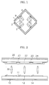
- Fig. 1 illustrates a schematic view of opening patterns formed at pixel and common electrodes in a prior art liquid crystal display.
- the pixel and common electrodes are formed with opening patterns 1 and 2, respectively.
- Each of the opening patterns 1 and 2 is formed in a V-shape and is arranged with ends of the V-shapes in proximity to one another so that roughly a diamond shape is formed by the opening patterns 1 and 2.
- Liquid crystal material is injected between the pixel and common electrodes, and liquid crystal molecules 3 are aligned perpendicular to the electrodes.
- the liquid crystal molecules 3 When an electric field is applied to the liquid crystal material, the liquid crystal molecules 3 come to be arranged parallel to the electrodes. However, the response speed of the liquid crystal molecules 3 with respect to the applied electric field is very slow with the formation of the opening patterns 1 and 2 at the pixel and common electrodes. That is, as a result of a fringe field formed due to the opening patterns 1 and 2, the liquid crystal molecules 3 are first arranged perpendicular to the opening patterns 1 and 2 (A state), then aligned to be parallel thereto (B state) due to the inherent tendency of long axes of liquid crystal molecules to align themselves roughly parallel. Because of these two alignment steps, a slow response speed results.
- the slow response speed of liquid crystal molecules causes afterimages when displaying moving pictures on the screen. There is therefore a need to increase the response speed of liquid crystal molecules.
- Fig. 2 is a schematic cross sectional view of a liquid crystal display according to an example useful for understanding of the present invention.
- the liquid crystal display includes lower and upper substrates 10 and 20 arranged substantially in parallel with a predetermined gap therebetween.
- Liquid crystal material is injected between the lower and upper substrates 10 and 20 to form a liquid crystal layer, the liquid crystal material being comprised of liquid crystal molecules 30.
- a long axis of liquid crystal molecules 30 is oriented normal to the lower and upper substrates 10 and 20.
- Both the lower and upper substrates 10 and 20 are formed from a transparent material such as glass.
- the lower substrate 10 is overlaid with a pixel electrode 12 that is connected to a switching element 11 to receive display signals.
- the pixel electrode 12 is formed from a transparent material such as indium tin oxide (ITO) or indium zinc oxide (IZO), and has an opening pattern (not shown).
- the switching element 11 is, for example, a thin film transistor, and is connected to a gate line (not shown), which transmits scanning signals, and a data line (not shown), which transmits picture signals.
- the switching element 11 turns the pixel electrode 12 on and off.
- a lower polarizer film 14 is adhered to an outer surface of the lower substrate 10. If the pixel electrode 12 is formed from non-transparent material as in the reflection-type liquid crystal display, the lower polarizer film 14 is not needed.
- An inner surface of the upper substrate 20 is sequentially overlaid with a black matrix 21 for preventing the leakage of light, a color filter 22, and a common electrode 23.
- the common electrode 23 is formed of a transparent material such as ITO or IZO, and has an opening pattern (not shown).
- a polarizer film 24 is adhered to an outer surface of the upper substrate 20.
- the black matrix 21 or the color filter 22 may be formed on the lower substrate 10.
- the LCD can be structured to operate in a normally black mode by arranging the lower and upper polarizer films 14 and 24 so that lines formed on the lower polarizer film 14 are perpendicular to lines formed on the upper polarizer film 24, or can be structured to operate in a normally white mode by arranging the lower and upper polarizer films 14 and 24 with their lines parallel to each other.
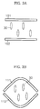
- Fig. 3A shows a schematic view of opening patterns of the pixel and common electrodes 12 and 23 according to a first example useful for understanding of the present invention. As shown in Fig.
- opening patterns 101 and 102 respectively of the pixel and common electrodes 12 and 23 are each formed in a straight line, the opening pattern 101 being substantially parallel to the opening pattern 102.
- the liquid crystal molecules 30 are arranged in parallel as a result of a fringe field generated by the opening patterns 101 and 102. Furthermore, the movement of the liquid crystal molecules 30 into the parallel arrangement is performed in a single step, thereby enabling a rapid response speed.
- white afterimage refers to a phenomenon in which a portion of the screen, where a dark color has been displayed on a bright background then returned to the color of the bright background, momentarily becomes brighter than the the bright background.
- Fig. 3B shows a schematic view of opening patterns of the pixel and common electrodes 12 and 23 according to the second example.
- opening patterns 111 and 112 respectively of the pixel and common electrodes 12 and 23 are each formed in a curved shape, with ends of the opening patterns 111 and 112 positioned in close proximity and centers bulging in opposite directions.
- the movement of the liquid crystal molecules 30 cannot be completed in a single step, resulting in a slow response speed.
- opening patterns of the pixel and common electrodes 12 and 23 will be described with reference to one pixel area.
- the pixel electrode 12 is substantially rectangular in shape having first and second long sides, respectively corresponding to left and right sides (in the drawings) of the pixel electrode 12; first and second short sides, respectively corresponding to top and bottom sides (in the drawings) of the pixel electrode 12; a first corner formed by ends of the first long side and the first short side; a second corner formed by ends of the first short side and the second long side; a third corner formed by ends of the second long side and the second short side; and a fourth corner formed by ends of the first long side and the second short side.
- the pixel electrode 12 includes an upper region and a lower region, the upper region corresponding to an upper half (in the drawings) of the pixel electrode 12 and defined by the first long side, the second long side and the first short side, and the lower region corresponding to a lower half (in the drawings) of the pixel electrode 12 and defined by the first long side, the second long side and the second short side.
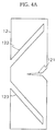
- Fig. 4A shows a schematic view of an opening pattern of the pixel electrode 12 according to a third example useful for understanding of the present invention. As shown in Fig.
- a middle opening 121 is formed inwardly from the first long side where the upper and lower regions of the pixel electrode 12 meet.
- the middle opening 121 extends a predetermined distance toward the second long side while being tapered.
- the first long side is cut at a predetermined angle on both sides of the middle opening 121 such that a wide inlet area of the middle opening 121 is formed.
- Upper and lower openings 122 and 123 are formed in the upper and lower regions of the pixel electrode 12, respectively, proceeding from the second long side at a predetermined angle respectively toward the first and fourth corners of the pixel electrode 12 in a symmetrical manner.
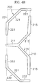
- Fig. 4B shows a schematic view of an opening pattern of the common electrode 23 according to the third example.
- the opening pattern of the common electrode 23 includes middle, upper and lower openings 210, 220 and 230 spaced apart from each at predetermined distances.
- the middle opening 210 includes a trunk 211 positioned where the upper and lower regions of the common electrode 23 meet and proceeding from the second long side a predetermined distance toward the first long side.
- First and second branches 212 and 214 are extended at a predetermined angle from the trunk 211 toward the first long side, and first and second sub-branches 213 and 215 extend along the first long side from the first and second branches 212 and 214, respectively, toward the first and second short sides, respectively.
- the upper opening 220 which is formed in the upper region of the common electrode 23, includes a first body 221 that is formed extended from the second long side to the first short side at a predetermined distance from the second corner and parallel to the first branch 212.
- a first upper limb 222 extends from an end of the first body 221 along the first short side and until reaching the first long side, and a first lower limb 223 extends from an opposite end of the first body 221 along the second long side toward the second short side.
- the lower opening 230 includes a second body 231, a second lower limb 232, and a second upper limb 233.
- the lower opening 230 is arranged in the lower region and is symmetrical to the upper opening 220.
- Fig. 4C shows a schematic view of the opening patterns of the pixel and common electrodes 12 and 23 shown respectively in Figs. 4A and 4B in an overlapped state.
- the opening patterns of the pixel and common electrodes 12 and 23 divide the pixel electrode 12 into several regions.
- the openings 121, 122 and 123 of the pixel electrode 12 and the openings 210, 220 and 230 of the common electrode 23 are alternately arranged except where the trunk 211 of the middle opening 210 of the common electrode partially overlaps the middle opening 121 of the pixel electrode 12.
- the lower and upper polarizer films 14 and 24 are arranged such that their polarizing directions are respectively 0° and 90° (or vice versa) with respect to the first and second short sides of the pixel electrode 12.
- the liquid crystal molecules 30 are rearranged under the application of an electric field, they are prevented from orienting in the polarizing direction of the polarizer films 14 and 24 so that the problem of texture does not occur.
- the movement of the liquid crystal molecules 30 is completed in one step, resulting in a rapid response speed.
- the opening portions of the pixel and common electrodes 12 and 23 are arranged generally in two directions normal to each other. Since the opening portions of the pixel and common electrodes 12 and 23 are alternately arranged, the fringe field is applied in four directions at one pixel area. Therefore, wide viewing angles can be obtained in all directions.
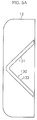
- Fig. 5A shows a schematic view of an opening pattern of the pixel electrode 12 according to a fourth example useful for understanding of the present invention.
- the opening pattern of the pixel electrode 12 is a V-shaped opening130.
- the V-shaped opening 130 has a vertex in proximity to the second long side and positioned where the upper region meets the lower region of the pixel electrode 12, and opens toward the first long side of the pixel electrode 12.
- an upper half 131 of the opening 130 extends at a predetermined angle from the vertex of the opening 130 toward the first long side of the pixel electrode 12 such that the upper half 131 is positioned wholly in the upper region of the pixel electrode 12, and a lower half 132 of the opening 130 extends at a predetermined angle from the vertex of the opening 130 toward the first long side of the pixel electrode 12 such that the lower half 132 is positioned wholly in the lower region of the pixel electrode 12.
- the second and third corners of the pixel electrode 12 are cut away to form a curved shape.
- Fig. 5B shows a schematic view of an opening pattern of the common electrode 23 according to the fourth example. As shown in Fig.
- the opening pattern of the common electrode 23 includes a right opening 240 and a left opening 250.
- the right opening 240 includes a base 241 formed along and extending past the first long side of the common electrode 23, and which tapers from a middle portion along the first long side toward the first and second short sides.
- the base 241 of the right opening 240 also includes a projection 242 extending a predetermined distance from the base 241 toward the second long side and tapered in the same direction. A portion of the projection 242 adjacent to the base 241 is formed at a predetermined slant.
- the left opening 250 includes a body 251 formed along the second long side of the common electrode 23, an upper limb 252 extended at a predetermined angle from one end of the body 251 toward and continuing past the first corner of the common electrode 23, and a lower limb 253 extended at a predetermined angle from the other end of the body 251 toward and continuing past the fourth corner of the common electrode 23. Centers of both the right and left openings 240 and 250 are positioned where the upper and lower regions of the common electrode 23 meet.
- Fig. 5C shows a schematic view of the opening patterns of the pixel and common electrodes 12 and 23 shown respectively in Figs. 5A and 5B in an overlapped state.
- the opening patterns of the pixel and common electrodes 12 and 23 divide the pixel electrode 12 into several regions.
- the V-shaped opening 130 of the pixel electrode 12 is placed between the right and left openings 240 and 250 of the common electrode 23.
- the upper and lower parts 131 and 132 of the V-shaped opening 130 proceed in parallel to the lower and upper limbs 252 and 253 of the left opening 250, respectively, as well as to the portion of the projection 242 adjacent to the base 241 of the right opening portion 240.
- An end of the projection 242 overlaps the vertex of the V-shaped opening portion 130.
- the lower and upper polarizer films 14 and 24 are arranged such that their polarizing directions are the same as in the third example.
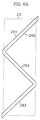
- Fig. 6A shows a schematic view of an opening pattern of the pixel electrode 12 according to a fifth example useful for understanding of the present invention.
- the opening pattern of the pixel electrode 12 includes an upper opening 141 formed in the upper region of the pixel electrode 12, and a lower opening 142 formed in the lower region of the pixel electrode. If the pixel electrode 12 is divided into three areas of equal length, that is, first to third areas, with the first area having as its one side the first short side, the third area having as its one side the second short side, and the second area being formed between the first and third areas, the upper opening 141 is positioned where the first and second areas meet, and the lower opening 142 is positioned where the second and third areas meet.
- the upper opening 141 extends from the first long side to the second long side of the pixel electrode 12 in the horizontal direction, and areas of the pixel electrode 12 corresponding to where the upper opening 141 is positioned along the first long side are cut away to form a curved shape.
- the lower opening 142 extends from the second long side to the first long side of the pixel electrode 12 in the horizontal direction, and areas of the pixel electrode 12 corresponding to where the lower opening 142 is positioned along the second long side are cut away to form a curved shape.
- second and third corners of the pixel electrode 12 are cut such that they are rounded.
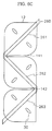
- Fig. 6B shows a schematic view of an opening pattern of the common electrode 23 according to the fifth example. As shown in Fig.
- the opening pattern of the common electrode 23 is a zigzag-shaped opening 260.
- the zigzag-shaped opening 260 includes an upper part 261 proceeding from the first corner of the common electrode 23 at a predetermined slant toward and meeting the second long side of the common electrode 23, a middle part 262 extended at a predetermined slant from an end of the upper part 261 where the same meets the second long side toward and meeting the first long side of the common electrode 23, and a lower part 263 extended at a predetermined slant from an end of the middle part 262 where the same meets the first long side toward and meeting the third corner of the common electrode 23.
- the common electrode 23 is divided into three areas of equal length, that is, first to third areas, with the first area having as its one side the first short side, the third area having as its one side the second short side, and the second area being formed between the first and third areas, the upper and middle parts 261 and 262 converge where the first and second areas meet, and the middle and lower parts 262 and 263 converge where the second and third areas meet.
- Fig. 6C shows a schematic view of the opening patterns of the pixel and common electrodes 12 and 23 shown respectively in Figs. 6A and 6B in an overlapped state.
- the opening patterns of the pixel and common electrodes 12 and 23 divide the pixel electrode 12 into several regions.
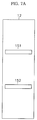
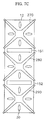
- FIG. 7A shows a schematic view of an opening pattern of the pixel electrode 12 according to a sixth example useful for understanding of the present invention.
- the opening pattern of the pixel electrode 12 includes an upper opening 151 formed parallel to the first and second short sides in the upper region of the pixel electrode 12, and a lower opening 152 also formed parallel to the first and second short sides in the lower region of the pixel electrode 12.
- the upper opening 151 is positioned where the first and second areas meet, and the lower opening portion 152 positioned where the second and third areas meet.
- the upper and lower openings 151 and 152 extend from a position in proximity to the first long side to a position in proximity to the second long side.
- Fig. 7B shows a schematic view of an opening pattern of the common electrode 23 according the sixth example. As shown in Fig.
- the opening pattern of the common electrode 23 includes first, second and third X-shaped openings 270, 280 and 290 spaced apart from each other at a predetermined distance along the length of the common electrode 23.
- a center area of each of the X-shaped openings 270, 280 or 290 is cut away to form an enlarged area approximately rectangular in shape.
- One line forming the "X" of the first X-shaped opening 270 extends from the first corner to the second long side of the common electrode 23 and its other line extends from the second corner to the first long side of the common electrode 23;
- one line forming the "X" of the second X-shaped opening 280 extends from the first long side to the second long side of the common electrode 23 and its other line extends from the second long side to the first long side of the common electrode 23;
- one line forming the "X" of the third X-shaped opening 290 extends from the second long side to the fourth corner of the common electrode 23 and its other line extends from the first long side to the third corner of the common electrode 23.
- Fig. 7C shows a schematic view of the opening patterns of the pixel and common electrodes 12 and 23 shown respectively in Figs. 7A and 7B in an overlapped state. As shown in Fig. 7C , the opening patterns of the pixel and common electrodes 12 and 23 are alternately arranged, and divide the pixel electrode 12 into several regions.
- Fig. 8A shows a schematic view of an opening pattern of the pixel electrode 12 according to a seventh example useful for understanding of the present invention.
- the opening pattern of the pixel electrode 12 includes an upper opening 160 formed in the upper region of the pixel electrode 12, and a lower opening 170 formed in the lower region of the pixel electrode 12.
- the upper opening 160 is T-shaped.
- the upper opening 160 has a base 161 (the top of the "T") formed at a predetermined distance from where the upper and lower regions of the pixel electrode 12 meet, the base 161 extending from approximately the first long side to the second long side of the pixel electrode 12.
- the upper opening 160 also has a protrusion 162 extending substantially from a center of the base 161 in a direction toward the first short side of the pixel electrode 12, thereby bisecting the upper region of the pixel electrode 12 into left and right sub-areas.
- the lower opening 170 is formed parallel to the base 161 of the upper opening 160 and extends across the pixel electrode 12 approximately and at predetermined distances from the first long side to the second long side of the pixel electrode 12 such that the lower opening 170 bisects the lower region of the pixel electrode 12 into upper and lower sub-areas.
- Fig. 8B shows a schematic view of an opening pattern of the common electrode 23 according to the seventh example. As shown in Fig. 8B , the opening pattern of the common electrode 23 includes two upper openings 310 and 320, a middle opening 330, and a lower opening 340.
- the two upper openings 310 and 320 are spaced apart from each other at a predetermined distance in the upper region of the common electrode 23, and are parallel to each other and to the first and second long sides of the common electrode 23.
- the middle and lower openings 330 and 340 are spaced apart from each other at a predetermined distance in the lower region of the common electrode 23, and are parallel to each other and to the first and second short sides of the common electrode 23. Both end portions of the middle and lower openings 330 and 340 are enlarged in roughly a triangular shape, and the triangle-shaped end portions of the middle and lower opening portions 330 and 340 proceed over the first and second long sides of the common electrode 23.
- Fig. 8C shows a schematic view of the opening patterns of the pixel and common electrodes 12 and 23 shown respectively in Figs. 8A and 8B in an overlapped state.
- the opening patterns of the pixel and common electrodes 12 and 23 divide the pixel electrode 12 into several regions. That is, ends of the upper opening portions 310 and 320 of the common electrode 23 farthest from the first short side of the common electrode 23 overlap the base 161 of the T-shaped opening 160 of the pixel electrode 12.
- the upper openings 310 and 320 of the common electrode 23, and the protrusion 162 of the T-shaped opening 160 of the pixel electrode 12 divide an area of the pixel electrode 12 defined by the base 161 of the T-shaped opening 160, the first and second long sides of the pixel electrode 12, and the first short side of the pixel electrode 12 into four sub-areas.
- the middle and lower openings 330 and 340 of the common electrode 23, and the lower opening 170 of the pixel electrode 12 divide an area of the pixel electrode 12 defined by the base 161 of the T-shaped opening 160, the first and second long sides of the pixel electrode 12, and the second short side of the pixel electrode 12 into four sub-areas.
- the lower and upper polarizer films 14 and 24 are arranged such that their polarizing directions are the same as in the sixth example. Accordingly, the orienting direction of the liquid crystal molecules 30 becomes 45° with respect to the polarizing direction of the polarizer films 14 and 24 so that the response speed is rapid and the occurrence of texture is decreased, resulting in enhanced picture quality.
- the opening portions of the pixel and common electrodes 12 and 23 proceed generally in two directions normal to each other. Furthermore, as the opening portions of the pixel and common electrodes 12 and 23 are alternately arranged, the fringe field in one pixel area is applied in all directions.
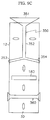
- Fig.- 9A shows a schematic view of an opening pattern of the pixel electrode 12 according to an eighth example useful for understanding of the present invention.
- the opening pattern of the pixel electrode 12 is a single linear opening 180 parallel to the first and second short sides of the pixel electrode 12. If the pixel electrode 12 is divided into three areas of equal length, that is, first to third areas, with the first area having as its one side the first short side, the third area having as its one side the second short side, and the second area being formed between the first and third areas, the linear opening 180 is positioned where the second and third areas meet.
- Fig. 9B shows a schematic view of an opening pattern of the common electrode 23 according to the eighth example.
- the opening pattern of the common electrode 23 includes an upper opening 350 formed in the upper region of the common electrode 23 and a lower opening 360 formed in the lower region of the common electrode.
- the upper opening 350 includes a base 351, a trunk 352, and two branches 353 and 354.
- the base 351 of the upper opening 350 is formed roughly in a triangular shape and positioned extending over and past the first short side of the common electrode 23.
- the trunk 352 is linearly extended from an apex of the base 351 in a direction toward the second short side of the common electrode 23.
- the branches 353 and 354 are branched from a distal end of the trunk 352 toward and extending over the first and second long sides of the common electrode 23, each of the branches 353 and 354 forming an obtuse angle with respect to the trunk 352.
- the lower opening 360 linearly proceeds in a direction parallel to the first and short sides of the common electrode 23. Both ends of the lower opening 360 are enlarged in roughly a triangular shape and extend over the first and second long sides of the common electrode 23.
- Fig. 9C shows a schematic view of the pixel and common electrodes 12 and 23 shown respectively in Figs. 9A and 9B in an overlapped state.
- the branches 353 and 354 of the upper opening 350 of the common electrode 23 roughly divide the pixel electrode 12 into upper and lower areas.
- the trunk 352 of the upper opening 350 of the common electrode 23 bisects the upper area of the pixel electrode 12 into two sub-areas, one sub-area having as its one side the second long side of the pixel electrode 12 and the other sub-area having as its one side the first long side of the pixel electrode 12.
- the lower opening 360 of the common electrode 23, and the linear opening 180 of the pixel electrode 12 trisect the lower area of the pixel electrode 12 into upper, middle and lower sub-areas.
- the lower and upper polarizer films 14 and 24 are arranged such that their polarizing directions are the same as in the sixth example. With this structure, effects similar to those obtained in the seventh example are realized.
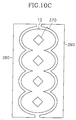
- Fig. 10A shows a schematic view of an opening pattern of the pixel electrode 12 according to a preferred embodiment of the present invention.
- the pixel electrode 12 is formed of four oval-shaped portions sequentially interconnected in the longitudinal direction.
- Fig. 10B shows a schematic view of an opening pattern of the common electrode 23 according to the preferred embodiment of the present invention.
- the opening pattern of the common electrode 23 includes four diamond-shaped openings 370, and left and right openings 380 and 390 surrounding the diamond-shaped openings 370.
- the diamond-shaped openings 370 are arranged over a longitudinal center of the common electrode 23 and are spaced apart from each other at a predetermined distance. Inner sides of the left and right openings 380 and 390 facing the diamond-shaped openings 370 substantially form cycloids such that four partial ovals result, each oval surrounding one of the diamond-shaped openings 370.
- Fig. 10C shows a schematic view of the pixel electrode 12 and the common electrode 23 shown respectively in Figs. 10A and 10B in an overlapped state.
- each diamond-shaped opening 370 of the common electrode 23 is placed at the center of the corresponding oval-shaped portion of the pixel electrode 12.
- the left and right openings 380 and 390 of the common electrode 23 surround the pixel electrode 12 at a predetermined distance.
- the lower and upper polarizer films 14 and 24 are arranged such that their polarizing directions are the same as in the third example.
- the opening patterns of the pixel and common electrodes 12 and 23 according to the third to eighth examples and the preferred embodiment were designed with the intent of maximally satisfying the following conditions, the conditions being particular to opening patterns of the type for obtaining the partitioned orientation of the liquid crystal molecules 30.
- disclination or texture should not be generated outside of the partitioned regions. Disclination occurs when the long axes of liquid crystal molecules are oriented in various directions in a confined area, particularly when the long axes are inclined toward one another. Therefore, it is preferable that the opening patterns of the pixel and common electrodes 12 and 23 are alternately arranged, and the end portions of the opening patterns are adjacent to each other. That is, when viewed from above, the opening patterns of the pixel and common electrodes 12 and 23 are preferably structured in the form of closed polygons. Furthermore, since disinclination is prone to occur when the opening patterns are structured having acute angles, it is preferable that the opening patterns are formed including only obtuse angles.
- a stable partitioned orientation of liquid crystal molecules also enhances brightness.
- the leakage of light occurs in an off state, and dark portions are generated in an on state. Also, this dispersion of the orientation of liquid crystal molecules causes the generation of afterimages when the liquid crystal molecules are rearranged.
- the angle made by the two directors of the liquid crystal molecules 30 at adjacent partitioned regions is preferably about 90°.
- the angle of the director is established in this manner, disclination occurs only at the narrowest areas.
- the brightness is highest when the angle between the light transmission axis of the polarizer film and the director for liquid crystal molecules is 45°. It is preferable that twisting or bending of the opening patterns of the pixel and common electrodes 12 and 23 is minimized as much as possible.
- the opening patterns of the pixel and common electrodes 12 and 23 are not twisted or bent too much. That is, it is preferable that the opening patterns of the pixel and common electrodes 12 and 23 linearly face each other. The affect of an opening width of the opening patterns and a spacing interval between the openings on light transmission and response speed will now be described.
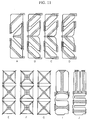
- FIG. 11 shows schematic views of nine different opening patterns A - J for demonstrating the affect of opening pattern width and spacing on response speed and brightness.
- the opening patterns of the common electrode are indicated by diagonal lines
- the opening patterns of the pixel electrode are indicated by solid lines.
- the B, C and D opening patterns are identical and the E, F and G opening patterns are identical. However, these opening patterns differ in opening width and spacing.
- the I and J opening patterns differ in the number of openings used, effectively having different opening spacings.
- the A opening pattern has a shape similar to that of the B, C and D opening patterns except for the formation at a center area of the A opening pattern. As a result, the A opening pattern is different in opening spacing from the B, C and D opening patterns.
- the opening width and the opening spacing of each opening pattern are listed in Table 1.
- Fig. 12A is a graph illustrating light transmissivity levels of test cells applying the A through J opening patterns
- Fig. 12A is a graph illustrating light transmissivity levels of test cells applying the A through J opening patterns
- FIG. 12B is a graph comparing the light transmissivity level of a test cell applying the B opening pattern to the light transmissivity levels of test cells applying the A through J opening patterns. As shown in the graphs, the light transmissivity level of the test cell applying the G opening pattern is the highest, exceeding 13%. If the light transmissivity levels of the test cells are ranked from highest to lowest according to which opening pattern is used, the following ranking results: G, E, I, B, D, A, C, F, and J.
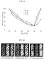
- Fig. 13 is a graph illustrating response times as a function of gray scale of test cells applying the A through J opening patterns. Although only sixty-nine (69) gray scales are used in actual application, the experiment was performed with one hundred and ten (110) gray scales.
- response times of the test cells applying the B, C, D, and J opening patterns were relatively fast over the whole range of gray scales.
- the response times were relatively slow.
- the slow response times were due to the movement of texture, and in the case of the test cells applying the E, F, and G opening patterns, the slow response times can be attributed to the two-step movement of liquid crystal molecules.
- the results of the experiment performed with the actual panels were similar to the results when using the test cells. However, there were some differences as follows. First, the actual panel in which the I opening pattern was applied exhibited a higher response speed than the test cell applying the same opening pattern. Also, better results with regard to brightness were obtained with the actual panel applying the J opening pattern than when the test cell was used. Specifically, the brightness of the test cell applying the J opening pattern was 75% of the cell applying the B opening pattern, whereas this was increased to 90% when the J opening pattern was applied to the actual panel.
- the opening patterns to select depending on what the intended area of improvement is as follows. If the improvement of brightness and the minimization of white afterimages are what are desired, it is preferable to use the B, D, E, and I opening patterns. However, if an improvement in response speed while keeping the brightness at a normal level is desired, the B, D, and I opening patterns are preferred. Finally, if what is needed is solely an improvement in response speed (without concerning brightness), the D and J opening patterns are preferred.
- Fig. 14 is a graph illustrating response times as a function of gray scale of actual panels applying the B, C, and D opening patterns. As shown in the graph, the response times of the panels applying the opening patterns exhibited the following relation (based on the type of opening pattern) when 20 to 40 gray scales were used: D ⁇ B ⁇ C. It is evident, therefore, that the larger the width of the opening pattern the faster the response time.
- the response time of the panel applying the C opening pattern is shorter than that of the panel applying B opening pattern, and after 45 gray scales, the response time of the panel applying the C opening pattern is shorter than that of the panel applying the D opening pattern.
- a change in the response time of the panel applying the C opening pattern is not actually taking place, but instead is given the appearance of change as a result of the generation of white afterimages. That is, the response waveform is distorted due to the white afterimages so that the response time seems to be shorter than it actually is. Accordingly, the conclusion originally reached that the larger the width of the opening pattern the faster the response speed remains valid.
- Figs. 15A to 15C are photographs of the C, B and D opening patterns, respectively, at white gray scales.
- the C opening pattern with poor texture stability displays the lowest level of brightness, with the B and D opening patterns exhibiting similarly higher levels of brightness.
- the D opening pattern exhibits a low opening ratio due to its significant width, but displays good texture stability such that panels applying this opening pattern have a high brightness. Texture stability is determined by the intensity of the fringe field and the width of the opening pattern.
- the boundary areas between adjacent partitioned regions in the C, B and D opening patterns are formed differently. That is, two clearly distinguishable textures are present in most of the boundary areas of the C opening pattern, and with the B opening pattern, the boundary areas are again distinguishable but not as clearly as with the C opening pattern.
- the boundary areas of the D opening pattern are not clearly formed and are faint in many portions.
- Figs. 16A and 16B are photographs of the C and D opening patterns applied to test cells in which a change in the partitioned regions according to a level of an applied voltage is shown.
- Figs. 17A and 17B are schematic views used to illustrate the change in intensity of a fringe field according to variations in opening pattern width.
- the horizontal component of the fringe field experiences corresponding increases.
- the horizontal component of the fringe field plays an important role in determining the orienting direction of liquid crystal molecules. Therefore, opening patterns with a large width are preferred in forming partitioned regions. In contrast, the larger the width of the opening pattern the weaker the intensity of the vertical component of the electric field working at the center of the opening pattern.
- Figs. 18A to 18D are schematic views illustrating orienting states of liquid crystal molecules at a peripheral portion of the opening patterns.
- the liquid crystal molecules are horizontally oriented to some degree even at the center area of the opening pattern. That is, they are slightly inclined when the applied voltage is low, but completely oriented in the horizontal direction when the applied voltage is high. This is due to the vertical component of the electric field being strong even at the center area of the opening pattern. As a result, the leakage of light occurs and the boundary area between the partitioned regions is formed by two separate lines. Furthermore, in case the orienting direction of the liquid crystal molecules is changed by 180°, elasticity becomes greater due to the small width of the opening pattern.
- the fringe field is not strong enough to overcome the elasticity, thereby resulting in the orienting direction of the liquid crystal molecules at the boundary areas becoming non-uniform between the partitioned regions. Such a non-uniform orientation of the liquid crystal molecules occurs even in micro regions of the pixel.
- the long axes of the liquid crystal molecules are perpendicular to the electrodes at the center area of the opening pattern.
- the liquid crystal molecules are slightly inclined, but the degree of inclination is less than when the opening pattern has a small width. Therefore, only a minimal amount of light leakage occurs and the boundary area between adjacent partitioned regions is shaped with a dark line.
- the width of the opening pattern is great, although the opening ratio is low, the orientation of the liquid crystal molecules is uniform such that a satisfactory degree of brightness is obtained.
- the opening width of the opening pattern is in the range of 13 ⁇ 3 ⁇ m, and the cell gap is in the range of about 4-6 ⁇ m.
- the affect of opening spacing on the optical characteristics of the opening patterns will now be described.
- the I and J opening patterns have the same total widths but effectively different spacings. According to the experimental results with respect to the test cells, the optical characteristics of the I and J opening patterns are significantly different. However, when actual panels apply these opening patterns, the resulting optical characteristics of the I and J opening patterns do not vary by such a degree. It is viewed that this is a result of the such factors as the difference in the type of alignment layer used, whether a protective insulating layer is used, the difference in the waveforms of the applied voltage, etc. However, when the speeds of moving picture images are compared in the actual panels, they are more rapid with the J opening pattern than with the I opening pattern. This can be easily demonstrated by observing the motion of a dark rectangle on a gray background. The only difference in response speed occurs by variations in the gray scales.
- the opening ratio is significantly reduced but the brightness does not undergo much change.
- the exception is with the I opening pattern in which even though the distance between the opening portions is large, a high brightness results because texture control is easily performed. In brief, a smaller distance between the opening portions results in an improvement of the response speed at various gray scales. Even though the brightness is prone to deteriorate due to the decrease in the opening ratio, this can be compensated for to some degree by controlling texture.
- Figs. 19 and 20 show schematic views of portions where texture occurs in the B and J opening patterns, respectively.
- the opening pattern shown in Fig. 19 is nearly identical to that shown in Fig. 4C .
- second and third openings 122 and 123 of the pixel electrode 12 begin from the first long side of the pixel electrode 12 and extend toward the second long side of the pixel electrode 12 nearly reaching the same, whereas in the opening pattern of Fig. 4C , the second and third openings 122 and 123 are structured in the opposite manner.
- portions of the second long side of the pixel electrode 12 adjacent to ends of the second and third openings 122 and 123 of the opening pattern of Fig. 19 are protruded externally to prevent the interconnection of the partitioned regions of the pixel electrode 12 from deteriorating due to the opening portions 122 and 123.
- the occurrence of texture is low, whereas when the substrates are inappropriately arranged, half moon-shaped textures, which do not cause the generation of white afterimages, occur.
- the width of the ends of the opening portions of the common electrode 23 may be enlarged. Through such enlargement, the allowable range of error in arrangement can be increased.
- the opening pattern shown in Fig. 20 is similar to that shown in Fig. 8C , but differs in the number of openings extending across the pixel electrode from the first long side to the second long side.
- the openings of the pixel electrode 12 are such that they are open where they begin at the first long side of the pixel electrode 12 and extend across toward, but not reaching, the second long side of the pixel electrode 12. Portions of the second long side of the pixel electrode 12 adjacent to ends of these openings are protruded externally.
- texture is concentrated at areas "a” corresponding to ends of openings of the common electrode 23 proceeding across from the first long side to the second long side of the common electrode 23. Furthermore, texture occurs also along the second short side of the pixel electrode 12, or area "b", which is deformed outwardly to enable a connection with the source electrode, as well as at area "c" at an end of an opening of the pixel electrode 12.
- Such texture can be inhibited in the following way.
- area a a width of the ends of the openings of the common electrode 23 are increased.
- area b the openings of the common electrode 23 are structured to overlap part of area b.
- area c the end of the opening of the pixel electrode 12 extended from the first short side is formed having sharp edges.
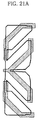
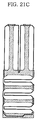
- Figs. 21A to 21C illustrate opening patterns where the above-described texture improving techniques have been applied.
- the opening patterns are formed at both the pixel and common electrodes 12 and 23 .
- the protrusions are formed using a gate insulating layer or a protective layer.
- the openings and the protrusions can be arranged as illustrated in Fig. 21 .
- the opening patterns may be formed only in the pixel electrode 12 while forming the protrusions in the common electrode 23.
- the openings and the protrusions can be arranged also as illustrated in Fig. 21 .
- the inventive liquid crystal display obtains a wide viewing angle, and exhibits stable orientation of the liquid crystal molecules and a rapid response speed.
Landscapes
- Physics & Mathematics (AREA)
- Nonlinear Science (AREA)
- Chemical & Material Sciences (AREA)
- Crystallography & Structural Chemistry (AREA)
- General Physics & Mathematics (AREA)
- Optics & Photonics (AREA)
- Mathematical Physics (AREA)
- Geometry (AREA)
- Spectroscopy & Molecular Physics (AREA)
- Liquid Crystal (AREA)
- Engineering & Computer Science (AREA)
- Microelectronics & Electronic Packaging (AREA)
Description
- The present invention relates to a liquid crystal display and, more particularly, to a liquid crystal display in which a predetermined opening pattern is formed at pixel and common electrodes such that a wide viewing angle is obtained.
- Generally, liquid crystal displays have a structure in which liquid crystal material is sandwiched between two substrates, and an electric field is applied to the liquid crystal material to control the alignment of molecules of the liquid crystal material, ultimately controlling the transmittance of incident light In VA liquid crystal displays, the liquid crystal molecules are aligned normal to the substrates when an electric field is not applied. In case two polarizer films are arranged with their lines (a plurality of which is formed in parallel on each polarizer film) perpendicular to each other, the linearly polarized light passed through the first polarizer film is completely blocked by the second polarizer film in the absence of an electric field. As such a liquid crystal display exhibits a very low brightness in an "off" state of the normally black mode, a relatively higher contrast ratio than that of the conventional TN liquid crystal display can be obtained.
- However, the liquid crystal molecules are irregularly inclined with respect to the substrate in the presence of an electric field such that one or more areas develop where the direction of the long axis of some of the liquid crystal molecules conforms to the polarizing direction of the first or second polarizer film. In such areas, the liquid crystal molecules cannot induce the rotation of the polarizing direction, i.e., polarization, and the light is completely blocked by the polarizer film. Such areas appear as black portions on the screen which cause a reduction in picture quality. These areas are referred to as areas of "texture".
- In order to solve the above problem, several electrode-patterning techniques have been suggested.
EP 0 884 626 A2 -
Fig. 1 illustrates a schematic view of opening patterns formed at pixel and common electrodes in a prior art liquid crystal display. As shown inFig. 1 , the pixel and common electrodes are formed withopening patterns opening patterns opening patterns liquid crystal molecules 3 are aligned perpendicular to the electrodes. - When an electric field is applied to the liquid crystal material, the
liquid crystal molecules 3 come to be arranged parallel to the electrodes. However, the response speed of theliquid crystal molecules 3 with respect to the applied electric field is very slow with the formation of theopening patterns opening patterns liquid crystal molecules 3 are first arranged perpendicular to theopening patterns 1 and 2 (A state), then aligned to be parallel thereto (B state) due to the inherent tendency of long axes of liquid crystal molecules to align themselves roughly parallel. Because of these two alignment steps, a slow response speed results. - The slow response speed of liquid crystal molecules causes afterimages when displaying moving pictures on the screen. There is therefore a need to increase the response speed of liquid crystal molecules.
- It is an object of the present invention to provide a liquid crystal display which has an improved response speed and a wide viewing angle.
- It is another object of the present invention to provide a liquid crystal display which produces improved picture images. These and other objects may be achieved by a liquid crystal display as defined in
claim 1. Further embodiments are defined in the dependent claims. - A more complete appreciation of the invention, and many of the attendant advantages thereof, will be readily apparent as the same becomes better understood by reference to the following detailed description when considered in conjunction with the accompanying drawings in which like reference symbols indicate the same or the similar components, wherein:
-
Fig. 1 is a schematic view of opening pattern units formed at common and pixel electrodes in a prior art liquid crystal display; -
Fig. 2 is a schematic cross sectional view of a liquid crystal display according to an example useful for understanding of the present invention; -
Fig. 3A is a schematic view of opening pattern units formed at common and pixel electrodes according to a first example useful for understanding of the present invention; -
Fig. 3B is a schematic view of opening pattern units formed at common and pixel electrodes according to a second example useful for understanding of the present invention; -
Fig. 4A is a schematic view of an opening pattern of a pixel electrode according to a third example useful for understanding of the present invention; -
Fig. 4B is a schematic view of an opening pattern of a common electrode according to the third example; -
Fig. 4C is a schematic view of the opening patterns of the pixel and common electrodes shown respectively inFigs. 4A and4B in an overlapped state; -
Fig. 5A is a schematic view of an opening pattern of a pixel electrode according to a fourth example useful for understanding of the present invention; -
Fig. 5B is a schematic view of an opening pattern of a common electrode according the fourth example; -
Fig. 5C is a schematic view of the opening patterns of the pixel and common electrodes shown respectively inFigs. 5A and5B in an overlapped state; -
Fig. 6A is a schematic view of an opening pattern of a pixel electrode according to a fifth example useful for understanding of the present invention; -
Fig. 6B is a schematic view of an opening pattern of a common electrode according to the fifth example; -
Fig. 6C is a schematic view of the opening patterns of the pixel and common electrodes shown respectively inFigs. 6A and6B in an overlapped state; -
Fig. 7A is a schematic view of an opening pattern of a pixel electrode according to a sixth example useful for understanding of the present invention; -
Fig. 7B is a schematic view of an opening pattern of a common electrode according to the sixth example; -
Fig. 7C is a schematic view of the opening patterns of the pixel and common electrodes shown respectively inFigs. 7A and7B in an overlapped state; -
Fig. 8A is a schematic view of an opening pattern of a pixel electrode according to a seventh example useful for understanding of the present invention; -
Fig. 8B is a schematic view of an opening pattern of a common electrode according to the seventh example; -
Fig. 8C is a schematic view of the opening patterns of the pixel and common electrodes shown respectively inFigs. 8A and8B in an overlapped state; -
Fig. 9A is a schematic view of an opening pattern of a pixel electrode according to an eighth example useful for understanding of the present invention; -
Fig. 9B is a schematic view of an opening pattern of a common electrode according to the eighth example; -
Fig. 9C is a schematic view of the opening patterns of the pixel and common electrodes shown respectively inFigs. 9A and9B in an overlapped state; -
Fig. 10A is a schematic view of an opening pattern of a pixel electrode according to a preferred embodiment of the present invention; -
Fig. 10B is a schematic view of an opening pattern of a common electrode according to the preferred embodiment of the present invention; -
Fig. 10C is a schematic view of the opening patterns of the pixel and common electrodes shown respectively inFigs. 10A and 10B in an overlapped state; -
Fig. 11 are schematic views of various types of opening patterns for demonstrating the affect of opening pattern width and spacing on response speed and brightness;Fig. 12A is a graph illustrating light transmissivity levels of test cells applying the opening patterns shown inFig. 11 ; -
Fig. 12B is a graph comparing the light transmissivity level of a test cell applying a specific opening pattern shown inFig. 11 to the light transmissivity levels of test cells applying the other opening patterns shown inFig. 11 ; -
Fig. 13 is a graph illustrating response times as a function of gray scale of test cells applying the opening patterns shown inFig. 11 ; -
Fig. 14 is a graph illustrating response times as a function of gray scale of actual panels applying specific opening patterns shown inFig. 11 ; -
Figs. 15A to 15C are photographs of specific opening patterns shown inFig. 11 at white gray scales; -
Figs. 16A and 16B are photographs of specific opening patterns shown inFig. 11 used to illustrate a change in partitioned regions according to a level of an applied voltage; -
Figs. 17A and 17B are schematic views used to illustrate the change in intensity of a fringe field according to variations in opening pattern width; -
Figs. 18A to 18D are schematic views illustrating orientation states of liquid crystal molecules at a peripheral portion of opening patterns; -
Figs. 19 and20 are schematic views of areas where texture occurs in specific opening patterns shown inFig. 11 ; andFigs. 21A to 21C are schematic views of opening patterns where texture improvement techniques have been applied. - Preferred embodiments of this invention will be explained with reference to the accompanying drawings.
-
Fig. 2 is a schematic cross sectional view of a liquid crystal display according to an example useful for understanding of the present invention. As shown inFig. 2 , the liquid crystal display includes lower andupper substrates upper substrates liquid crystal molecules 30. A long axis ofliquid crystal molecules 30 is oriented normal to the lower andupper substrates upper substrates - The
lower substrate 10 is overlaid with apixel electrode 12 that is connected to a switchingelement 11 to receive display signals. Thepixel electrode 12 is formed from a transparent material such as indium tin oxide (ITO) or indium zinc oxide (IZO), and has an opening pattern (not shown). The switchingelement 11 is, for example, a thin film transistor, and is connected to a gate line (not shown), which transmits scanning signals, and a data line (not shown), which transmits picture signals. The switchingelement 11 turns thepixel electrode 12 on and off. Alower polarizer film 14 is adhered to an outer surface of thelower substrate 10. If thepixel electrode 12 is formed from non-transparent material as in the reflection-type liquid crystal display, thelower polarizer film 14 is not needed. - An inner surface of the
upper substrate 20 is sequentially overlaid with ablack matrix 21 for preventing the leakage of light, acolor filter 22, and acommon electrode 23. Thecommon electrode 23 is formed of a transparent material such as ITO or IZO, and has an opening pattern (not shown). Apolarizer film 24 is adhered to an outer surface of theupper substrate 20. Alternatively, theblack matrix 21 or thecolor filter 22 may be formed on thelower substrate 10. - The LCD can be structured to operate in a normally black mode by arranging the lower and
upper polarizer films lower polarizer film 14 are perpendicular to lines formed on theupper polarizer film 24, or can be structured to operate in a normally white mode by arranging the lower andupper polarizer films Fig. 3A shows a schematic view of opening patterns of the pixel andcommon electrodes Fig. 3A , openingpatterns common electrodes opening pattern 101 being substantially parallel to theopening pattern 102. With this structure, theliquid crystal molecules 30 are arranged in parallel as a result of a fringe field generated by the openingpatterns liquid crystal molecules 30 into the parallel arrangement is performed in a single step, thereby enabling a rapid response speed. - However, with the use of the above structure, texture develops over a wide area of the screen. It is also possible for white afterimages to be generated on the screen. The term "white afterimage" refers to a phenomenon in which a portion of the screen, where a dark color has been displayed on a bright background then returned to the color of the bright background, momentarily becomes brighter than the the bright background.
-
Fig. 3B shows a schematic view of opening patterns of the pixel andcommon electrodes Fig. 3B , openingpatterns common electrodes patterns liquid crystal molecules 30 cannot be completed in a single step, resulting in a slow response speed. In the following examples and preferred embodiment, opening patterns of the pixel andcommon electrodes pixel electrode 12 is substantially rectangular in shape having first and second long sides, respectively corresponding to left and right sides (in the drawings) of thepixel electrode 12; first and second short sides, respectively corresponding to top and bottom sides (in the drawings) of thepixel electrode 12; a first corner formed by ends of the first long side and the first short side; a second corner formed by ends of the first short side and the second long side; a third corner formed by ends of the second long side and the second short side; and a fourth corner formed by ends of the first long side and the second short side. Further, thepixel electrode 12 includes an upper region and a lower region, the upper region corresponding to an upper half (in the drawings) of thepixel electrode 12 and defined by the first long side, the second long side and the first short side, and the lower region corresponding to a lower half (in the drawings) of thepixel electrode 12 and defined by the first long side, the second long side and the second short side. - As the
common electrode 23 is present over the entire surface of theupper substrate 20, a portion of thecommon electrode 23 roughly corresponding to thepixel electrode 12 in one pixel area will be described. Here, such portions of thecommon electrode 23 will be indicated by a dotted line and the identifying markers (i.e., upper region and lower region; first long side and second long side; first short side and second short side; and first, second, third and fourth corners) used for ease of explanation of thepixel electrode 12 will also apply to these portions of thecommon electrode 23 defined by the dotted lines.Fig. 4A shows a schematic view of an opening pattern of thepixel electrode 12 according to a third example useful for understanding of the present invention. As shown inFig. 4A , amiddle opening 121 is formed inwardly from the first long side where the upper and lower regions of thepixel electrode 12 meet. Themiddle opening 121 extends a predetermined distance toward the second long side while being tapered. The first long side is cut at a predetermined angle on both sides of themiddle opening 121 such that a wide inlet area of themiddle opening 121 is formed. Upper andlower openings pixel electrode 12, respectively, proceeding from the second long side at a predetermined angle respectively toward the first and fourth corners of thepixel electrode 12 in a symmetrical manner. -
Fig. 4B shows a schematic view of an opening pattern of thecommon electrode 23 according to the third example. As shown inFig. 4B , the opening pattern of thecommon electrode 23 includes middle, upper andlower openings middle opening 210 includes atrunk 211 positioned where the upper and lower regions of thecommon electrode 23 meet and proceeding from the second long side a predetermined distance toward the first long side. First andsecond branches trunk 211 toward the first long side, and first andsecond sub-branches second branches upper opening 220, which is formed in the upper region of thecommon electrode 23, includes afirst body 221 that is formed extended from the second long side to the first short side at a predetermined distance from the second corner and parallel to thefirst branch 212. A firstupper limb 222 extends from an end of thefirst body 221 along the first short side and until reaching the first long side, and a firstlower limb 223 extends from an opposite end of thefirst body 221 along the second long side toward the second short side. Thelower opening 230 includes asecond body 231, a secondlower limb 232, and a secondupper limb 233. Thelower opening 230 is arranged in the lower region and is symmetrical to theupper opening 220. -
Fig. 4C shows a schematic view of the opening patterns of the pixel andcommon electrodes Figs. 4A and4B in an overlapped state. As shown inFig. 4C , the opening patterns of the pixel andcommon electrodes pixel electrode 12 into several regions. Theopenings pixel electrode 12 and theopenings common electrode 23 are alternately arranged except where thetrunk 211 of themiddle opening 210 of the common electrode partially overlaps themiddle opening 121 of thepixel electrode 12. - In this example, the lower and
upper polarizer films pixel electrode 12. With such an arrangement, when theliquid crystal molecules 30 are rearranged under the application of an electric field, they are prevented from orienting in the polarizing direction of thepolarizer films liquid crystal molecules 30 are fully oriented in parallel under the influence of the fringe field, the movement of theliquid crystal molecules 30 is completed in one step, resulting in a rapid response speed. - In addition, the opening portions of the pixel and
common electrodes common electrodes -
Fig. 5A shows a schematic view of an opening pattern of thepixel electrode 12 according to a fourth example useful for understanding of the present invention. As shown inFig. 5A , the opening pattern of thepixel electrode 12 is a V-shaped opening130. The V-shapedopening 130 has a vertex in proximity to the second long side and positioned where the upper region meets the lower region of thepixel electrode 12, and opens toward the first long side of thepixel electrode 12. That is, anupper half 131 of theopening 130 extends at a predetermined angle from the vertex of theopening 130 toward the first long side of thepixel electrode 12 such that theupper half 131 is positioned wholly in the upper region of thepixel electrode 12, and alower half 132 of theopening 130 extends at a predetermined angle from the vertex of theopening 130 toward the first long side of thepixel electrode 12 such that thelower half 132 is positioned wholly in the lower region of thepixel electrode 12. Further, the second and third corners of thepixel electrode 12 are cut away to form a curved shape.Fig. 5B shows a schematic view of an opening pattern of thecommon electrode 23 according to the fourth example. As shown inFig. 5B , the opening pattern of thecommon electrode 23 includes aright opening 240 and aleft opening 250. Theright opening 240 includes a base 241 formed along and extending past the first long side of thecommon electrode 23, and which tapers from a middle portion along the first long side toward the first and second short sides. Thebase 241 of theright opening 240 also includes aprojection 242 extending a predetermined distance from the base 241 toward the second long side and tapered in the same direction. A portion of theprojection 242 adjacent to thebase 241 is formed at a predetermined slant. Theleft opening 250 includes abody 251 formed along the second long side of thecommon electrode 23, anupper limb 252 extended at a predetermined angle from one end of thebody 251 toward and continuing past the first corner of thecommon electrode 23, and alower limb 253 extended at a predetermined angle from the other end of thebody 251 toward and continuing past the fourth corner of thecommon electrode 23. Centers of both the right and leftopenings common electrode 23 meet. -
Fig. 5C shows a schematic view of the opening patterns of the pixel andcommon electrodes Figs. 5A and5B in an overlapped state. As shown inFig. 5C , the opening patterns of the pixel andcommon electrodes pixel electrode 12 into several regions. The V-shapedopening 130 of thepixel electrode 12 is placed between the right and leftopenings common electrode 23. The upper andlower parts opening 130 proceed in parallel to the lower andupper limbs left opening 250, respectively, as well as to the portion of theprojection 242 adjacent to thebase 241 of theright opening portion 240. An end of theprojection 242 overlaps the vertex of the V-shapedopening portion 130. With the configuration of the fourth example as described above, the lower andupper polarizer films -
Fig. 6A shows a schematic view of an opening pattern of thepixel electrode 12 according to a fifth example useful for understanding of the present invention. As shown inFig. 6A , the opening pattern of thepixel electrode 12 includes anupper opening 141 formed in the upper region of thepixel electrode 12, and alower opening 142 formed in the lower region of the pixel electrode. If thepixel electrode 12 is divided into three areas of equal length, that is, first to third areas, with the first area having as its one side the first short side, the third area having as its one side the second short side, and the second area being formed between the first and third areas, theupper opening 141 is positioned where the first and second areas meet, and thelower opening 142 is positioned where the second and third areas meet. Theupper opening 141 extends from the first long side to the second long side of thepixel electrode 12 in the horizontal direction, and areas of thepixel electrode 12 corresponding to where theupper opening 141 is positioned along the first long side are cut away to form a curved shape. Similarly, thelower opening 142 extends from the second long side to the first long side of thepixel electrode 12 in the horizontal direction, and areas of thepixel electrode 12 corresponding to where thelower opening 142 is positioned along the second long side are cut away to form a curved shape. In addition, second and third corners of thepixel electrode 12 are cut such that they are rounded.Fig. 6B shows a schematic view of an opening pattern of thecommon electrode 23 according to the fifth example. As shown inFig. 6B , the opening pattern of thecommon electrode 23 is a zigzag-shapedopening 260. The zigzag-shapedopening 260 includes anupper part 261 proceeding from the first corner of thecommon electrode 23 at a predetermined slant toward and meeting the second long side of thecommon electrode 23, amiddle part 262 extended at a predetermined slant from an end of theupper part 261 where the same meets the second long side toward and meeting the first long side of thecommon electrode 23, and alower part 263 extended at a predetermined slant from an end of themiddle part 262 where the same meets the first long side toward and meeting the third corner of thecommon electrode 23. If thecommon electrode 23 is divided into three areas of equal length, that is, first to third areas, with the first area having as its one side the first short side, the third area having as its one side the second short side, and the second area being formed between the first and third areas, the upper andmiddle parts lower parts -
Fig. 6C shows a schematic view of the opening patterns of the pixel andcommon electrodes Figs. 6A and6B in an overlapped state. As shown inFig. 6C , the opening patterns of the pixel andcommon electrodes pixel electrode 12 into several regions. The portion where the upper andmiddle parts opening 260 of thecommon electrode 23 meet overlaps an end of theupper opening portion 141 of thepixel electrode 12 adjacent to the second long side, and the portion where the middle andlower parts opening 260 of thecommon electrode 23 meet overlaps an end of thelower opening portion 142 of thepixel electrode 12 adjacent to the first long side. - With the configuration of the fifth example as described above, the lower and
upper polarizer films Fig. 7A shows a schematic view of an opening pattern of thepixel electrode 12 according to a sixth example useful for understanding of the present invention. As shown inFig. 7A , the opening pattern of thepixel electrode 12 includes anupper opening 151 formed parallel to the first and second short sides in the upper region of thepixel electrode 12, and alower opening 152 also formed parallel to the first and second short sides in the lower region of thepixel electrode 12. If thepixel electrode 12 is divided into three areas of equal length, that is, first to third areas, with the first area having as its one side the first short side, the third area having as its one side the second short side, and the second area being formed between the first and third areas, theupper opening 151 is positioned where the first and second areas meet, and thelower opening portion 152 positioned where the second and third areas meet. The upper andlower openings Fig. 7B shows a schematic view of an opening pattern of thecommon electrode 23 according the sixth example. As shown inFig. 7B , the opening pattern of thecommon electrode 23 includes first, second and thirdX-shaped openings common electrode 23. A center area of each of theX-shaped openings X-shaped opening 270 extends from the first corner to the second long side of thecommon electrode 23 and its other line extends from the second corner to the first long side of thecommon electrode 23; one line forming the "X" of the secondX-shaped opening 280 extends from the first long side to the second long side of thecommon electrode 23 and its other line extends from the second long side to the first long side of thecommon electrode 23; and one line forming the "X" of the thirdX-shaped opening 290 extends from the second long side to the fourth corner of thecommon electrode 23 and its other line extends from the first long side to the third corner of thecommon electrode 23. -
Fig. 7C shows a schematic view of the opening patterns of the pixel andcommon electrodes Figs. 7A and7B in an overlapped state. As shown inFig. 7C , the opening patterns of the pixel andcommon electrodes pixel electrode 12 into several regions. - With the configuration of the sixth example as described above, the lower and
upper polarizer films pixel electrode 12.Fig. 8A shows a schematic view of an opening pattern of thepixel electrode 12 according to a seventh example useful for understanding of the present invention. As shown inFig. 8A , the opening pattern of thepixel electrode 12 includes anupper opening 160 formed in the upper region of thepixel electrode 12, and alower opening 170 formed in the lower region of thepixel electrode 12. Theupper opening 160 is T-shaped. That is, theupper opening 160 has a base 161 (the top of the "T") formed at a predetermined distance from where the upper and lower regions of thepixel electrode 12 meet, thebase 161 extending from approximately the first long side to the second long side of thepixel electrode 12. Theupper opening 160 also has aprotrusion 162 extending substantially from a center of the base 161 in a direction toward the first short side of thepixel electrode 12, thereby bisecting the upper region of thepixel electrode 12 into left and right sub-areas. Thelower opening 170 is formed parallel to thebase 161 of theupper opening 160 and extends across thepixel electrode 12 approximately and at predetermined distances from the first long side to the second long side of thepixel electrode 12 such that thelower opening 170 bisects the lower region of thepixel electrode 12 into upper and lower sub-areas.Fig. 8B shows a schematic view of an opening pattern of thecommon electrode 23 according to the seventh example. As shown inFig. 8B , the opening pattern of thecommon electrode 23 includes twoupper openings middle opening 330, and alower opening 340. The twoupper openings common electrode 23, and are parallel to each other and to the first and second long sides of thecommon electrode 23. The middle andlower openings common electrode 23, and are parallel to each other and to the first and second short sides of thecommon electrode 23. Both end portions of the middle andlower openings lower opening portions common electrode 23. -
Fig. 8C shows a schematic view of the opening patterns of the pixel andcommon electrodes Figs. 8A and8B in an overlapped state. As shown inFig. 8C , the opening patterns of the pixel andcommon electrodes pixel electrode 12 into several regions. That is, ends of the upper openingportions common electrode 23 farthest from the first short side of thecommon electrode 23 overlap thebase 161 of the T-shapedopening 160 of thepixel electrode 12. Accordingly, theupper openings common electrode 23, and theprotrusion 162 of the T-shapedopening 160 of thepixel electrode 12 divide an area of thepixel electrode 12 defined by thebase 161 of the T-shapedopening 160, the first and second long sides of thepixel electrode 12, and the first short side of thepixel electrode 12 into four sub-areas. The middle andlower openings common electrode 23, and thelower opening 170 of thepixel electrode 12 divide an area of thepixel electrode 12 defined by thebase 161 of the T-shapedopening 160, the first and second long sides of thepixel electrode 12, and the second short side of thepixel electrode 12 into four sub-areas. - With the configuration of the seventh example as described above, the lower and
upper polarizer films liquid crystal molecules 30 becomes 45° with respect to the polarizing direction of thepolarizer films common electrodes common electrodes pixel electrode 12 according to an eighth example useful for understanding of the present invention. As shown inFig. 9A , the opening pattern of thepixel electrode 12 is a singlelinear opening 180 parallel to the first and second short sides of thepixel electrode 12. If thepixel electrode 12 is divided into three areas of equal length, that is, first to third areas, with the first area having as its one side the first short side, the third area having as its one side the second short side, and the second area being formed between the first and third areas, thelinear opening 180 is positioned where the second and third areas meet. -
Fig. 9B shows a schematic view of an opening pattern of thecommon electrode 23 according to the eighth example. As shown inFig. 9B , the opening pattern of thecommon electrode 23 includes anupper opening 350 formed in the upper region of thecommon electrode 23 and alower opening 360 formed in the lower region of the common electrode. Theupper opening 350 includes abase 351, atrunk 352, and twobranches base 351 of theupper opening 350 is formed roughly in a triangular shape and positioned extending over and past the first short side of thecommon electrode 23. Thetrunk 352 is linearly extended from an apex of the base 351 in a direction toward the second short side of thecommon electrode 23. Thebranches trunk 352 toward and extending over the first and second long sides of thecommon electrode 23, each of thebranches trunk 352. Thelower opening 360 linearly proceeds in a direction parallel to the first and short sides of thecommon electrode 23. Both ends of thelower opening 360 are enlarged in roughly a triangular shape and extend over the first and second long sides of thecommon electrode 23. -
Fig. 9C shows a schematic view of the pixel andcommon electrodes Figs. 9A and9B in an overlapped state. As shown inFig. 9C , thebranches upper opening 350 of thecommon electrode 23 roughly divide thepixel electrode 12 into upper and lower areas. Thetrunk 352 of theupper opening 350 of thecommon electrode 23 bisects the upper area of thepixel electrode 12 into two sub-areas, one sub-area having as its one side the second long side of thepixel electrode 12 and the other sub-area having as its one side the first long side of thepixel electrode 12. Thelower opening 360 of thecommon electrode 23, and thelinear opening 180 of thepixel electrode 12 trisect the lower area of thepixel electrode 12 into upper, middle and lower sub-areas. - With the configuration of the eighth example, the lower and
upper polarizer films -
Fig. 10A shows a schematic view of an opening pattern of thepixel electrode 12 according to a preferred embodiment of the present invention. As shown inFig. 10A , thepixel electrode 12 is formed of four oval-shaped portions sequentially interconnected in the longitudinal direction. -
Fig. 10B shows a schematic view of an opening pattern of thecommon electrode 23 according to the preferred embodiment of the present invention. As shown inFig. 10B , the opening pattern of thecommon electrode 23 includes four diamond-shapedopenings 370, and left andright openings openings 370. The diamond-shapedopenings 370 are arranged over a longitudinal center of thecommon electrode 23 and are spaced apart from each other at a predetermined distance. Inner sides of the left andright openings openings 370 substantially form cycloids such that four partial ovals result, each oval surrounding one of the diamond-shapedopenings 370. -
Fig. 10C shows a schematic view of thepixel electrode 12 and thecommon electrode 23 shown respectively inFigs. 10A and 10B in an overlapped state. As shown inFig. 10C , each diamond-shapedopening 370 of thecommon electrode 23 is placed at the center of the corresponding oval-shaped portion of thepixel electrode 12. Also, the left andright openings common electrode 23 surround thepixel electrode 12 at a predetermined distance. - With the configuration of the preferred embodiment of the present invention as described above, the lower and
upper polarizer films common electrodes liquid crystal molecules 30. - First, in order to obtain a maximum viewing angle, it is preferable that four partitioned regions for orienting the
liquid crystal molecules 30 are present within one pixel area. - Second, to obtain a stable partitioned orientation, disclination or texture should not be generated outside of the partitioned regions. Disclination occurs when the long axes of liquid crystal molecules are oriented in various directions in a confined area, particularly when the long axes are inclined toward one another. Therefore, it is preferable that the opening patterns of the pixel and
common electrodes common electrodes liquid crystal molecules 30 is dispersed, the leakage of light occurs in an off state, and dark portions are generated in an on state. Also, this dispersion of the orientation of liquid crystal molecules causes the generation of afterimages when the liquid crystal molecules are rearranged. - Third, in order to obtain a high level of brightness, the following conditions should be satisfied. The angle made by the two directors of the
liquid crystal molecules 30 at adjacent partitioned regions is preferably about 90°. When the angle of the director is established in this manner, disclination occurs only at the narrowest areas. The brightness is highest when the angle between the light transmission axis of the polarizer film and the director for liquid crystal molecules is 45°. It is preferable that twisting or bending of the opening patterns of the pixel andcommon electrodes - Finally, in order to obtain a rapid response speed of the
liquid crystal molecules 30, it is preferable again that the opening patterns of the pixel andcommon electrodes common electrodes - In order to investigate such an interrelation, nine panels, each with different opening patterns were made and tested.
Fig. 11 shows schematic views of nine different opening patterns A - J for demonstrating the affect of opening pattern width and spacing on response speed and brightness. In the drawing, the opening patterns of the common electrode are indicated by diagonal lines, and the opening patterns of the pixel electrode are indicated by solid lines. - As shown in
Fig. 11 , the B, C and D opening patterns are identical and the E, F and G opening patterns are identical. However, these opening patterns differ in opening width and spacing. The I and J opening patterns differ in the number of openings used, effectively having different opening spacings. The A opening pattern has a shape similar to that of the B, C and D opening patterns except for the formation at a center area of the A opening pattern. As a result, the A opening pattern is different in opening spacing from the B, C and D opening patterns. The opening width and the opening spacing of each opening pattern are listed in Table 1.Fig. 12A is a graph illustrating light transmissivity levels of test cells applying the A through J opening patterns, andFig. 12B is a graph comparing the light transmissivity level of a test cell applying the B opening pattern to the light transmissivity levels of test cells applying the A through J opening patterns. As shown in the graphs, the light transmissivity level of the test cell applying the G opening pattern is the highest, exceeding 13%. If the light transmissivity levels of the test cells are ranked from highest to lowest according to which opening pattern is used, the following ranking results: G, E, I, B, D, A, C, F, and J.Fig. 13 is a graph illustrating response times as a function of gray scale of test cells applying the A through J opening patterns. Although only sixty-nine (69) gray scales are used in actual application, the experiment was performed with one hundred and ten (110) gray scales. As shown in the graph, response times of the test cells applying the B, C, D, and J opening patterns were relatively fast over the whole range of gray scales. For the test cells applying the other opening patterns, the response times were relatively slow. In the case of the test cells applying the A and I opening patterns, the slow response times were due to the movement of texture, and in the case of the test cells applying the E, F, and G opening patterns, the slow response times can be attributed to the two-step movement of liquid crystal molecules. - The A through J opening patterns shown in
Fig. 11 were applied to actual panels and the panels were tested. Testing was performed on a total of four panels for each opening pattern. The results are listed in Table 2. - The results of the experiment performed with the actual panels were similar to the results when using the test cells. However, there were some differences as follows. First, the actual panel in which the I opening pattern was applied exhibited a higher response speed than the test cell applying the same opening pattern. Also, better results with regard to brightness were obtained with the actual panel applying the J opening pattern than when the test cell was used. Specifically, the brightness of the test cell applying the J opening pattern was 75% of the cell applying the B opening pattern, whereas this was increased to 90% when the J opening pattern was applied to the actual panel.
- When the actual panels were used, white afterimages were generated with the application of the C, I, and J opening patterns. The degree of white-afterimage generation was so high with the application of the C opening pattern that picture quality was impaired beyond a level that could be corrected. However, the generation of white afterimages was low enough when the I and J opening patterns were applied so that with some improvement, the panels could be used.
- On the basis of the above results, the opening patterns to select depending on what the intended area of improvement is are as follows. If the improvement of brightness and the minimization of white afterimages are what are desired, it is preferable to use the B, D, E, and I opening patterns. However, if an improvement in response speed while keeping the brightness at a normal level is desired, the B, D, and I opening patterns are preferred. Finally, if what is needed is solely an improvement in response speed (without concerning brightness), the D and J opening patterns are preferred.
- In order to further examine the interrelation between the response speed and the opening width of the opening patterns, the differences in the optical characteristics of panels applying the B, C, and D opening patterns, which have the same shape but different opening widths, will now be described.
-
Fig. 14 is a graph illustrating response times as a function of gray scale of actual panels applying the B, C, and D opening patterns. As shown in the graph, the response times of the panels applying the opening patterns exhibited the following relation (based on the type of opening pattern) when 20 to 40 gray scales were used: D<B<C. It is evident, therefore, that the larger the width of the opening pattern the faster the response time. - Roughly between 40 and 45 gray scales, the response time of the panel applying the C opening pattern is shorter than that of the panel applying B opening pattern, and after 45 gray scales, the response time of the panel applying the C opening pattern is shorter than that of the panel applying the D opening pattern. However, such a change in the response time of the panel applying the C opening pattern is not actually taking place, but instead is given the appearance of change as a result of the generation of white afterimages. That is, the response waveform is distorted due to the white afterimages so that the response time seems to be shorter than it actually is. Accordingly, the conclusion originally reached that the larger the width of the opening pattern the faster the response speed remains valid.
- With the
use 60 gray scales or more, the response speed slows considerably due to the occurrence of texture. In conclusion, the panel applying the D opening pattern, which has the greatest width, exhibits the most stable characteristics.Figs. 15A to 15C are photographs of the C, B and D opening patterns, respectively, at white gray scales. As seen from the photographs, the C opening pattern with poor texture stability displays the lowest level of brightness, with the B and D opening patterns exhibiting similarly higher levels of brightness. The D opening pattern exhibits a low opening ratio due to its significant width, but displays good texture stability such that panels applying this opening pattern have a high brightness. Texture stability is determined by the intensity of the fringe field and the width of the opening pattern. - The boundary areas between adjacent partitioned regions in the C, B and D opening patterns are formed differently. That is, two clearly distinguishable textures are present in most of the boundary areas of the C opening pattern, and with the B opening pattern, the boundary areas are again distinguishable but not as clearly as with the C opening pattern. The boundary areas of the D opening pattern, on the other hand, are not clearly formed and are faint in many portions.
-
Figs. 16A and 16B are photographs of the C and D opening patterns applied to test cells in which a change in the partitioned regions according to a level of an applied voltage is shown. - In the C opening pattern, two clearly distinguishable textures are present in the boundary areas when the applied voltage reaches 3.5V, and becomes clearer with further increases in the applied voltage. However, in the D opening pattern, the boundary areas are somewhat clearly distinguishable only when the applied voltage reaches 5V. Such distinguishable boundary areas are a result of the non-uniform orientation of the liquid crystal molecules. To better describe such a phenomenon, the intensity of the fringe field as a function of the widths of the opening patterns will be examined.
-
Figs. 17A and 17B are schematic views used to illustrate the change in intensity of a fringe field according to variations in opening pattern width. - As the width of the opening pattern becomes larger, the horizontal component of the fringe field experiences corresponding increases. The horizontal component of the fringe field plays an important role in determining the orienting direction of liquid crystal molecules. Therefore, opening patterns with a large width are preferred in forming partitioned regions. In contrast, the larger the width of the opening pattern the weaker the intensity of the vertical component of the electric field working at the center of the opening pattern.
-
Figs. 18A to 18D are schematic views illustrating orienting states of liquid crystal molecules at a peripheral portion of the opening patterns. When the width of the opening pattern is relatively small, the liquid crystal molecules are horizontally oriented to some degree even at the center area of the opening pattern. That is, they are slightly inclined when the applied voltage is low, but completely oriented in the horizontal direction when the applied voltage is high. This is due to the vertical component of the electric field being strong even at the center area of the opening pattern. As a result, the leakage of light occurs and the boundary area between the partitioned regions is formed by two separate lines. Furthermore, in case the orienting direction of the liquid crystal molecules is changed by 180°, elasticity becomes greater due to the small width of the opening pattern. In contrast, as the horizontal component of the fringe field is weak, the fringe field is not strong enough to overcome the elasticity, thereby resulting in the orienting direction of the liquid crystal molecules at the boundary areas becoming non-uniform between the partitioned regions. Such a non-uniform orientation of the liquid crystal molecules occurs even in micro regions of the pixel. - When the width of the opening pattern is relatively large, the long axes of the liquid crystal molecules are perpendicular to the electrodes at the center area of the opening pattern. As the applied voltage is increased, the liquid crystal molecules are slightly inclined, but the degree of inclination is less than when the opening pattern has a small width. Therefore, only a minimal amount of light leakage occurs and the boundary area between adjacent partitioned regions is shaped with a dark line.
- As described previously, the greater the width of the opening pattern the more rapid the response speed , and as stated above, a greater width of the opening pattern leads to more uniform micro regions of the pixel. When the width of the opening pattern is great, although the opening ratio is low, the orientation of the liquid crystal molecules is uniform such that a satisfactory degree of brightness is obtained. According to the above experimental results, it is preferable that the opening width of the opening pattern is in the range of 13± 3 µm, and the cell gap is in the range of about 4-6 µm.
- The affect of opening spacing on the optical characteristics of the opening patterns will now be described. The I and J opening patterns have the same total widths but effectively different spacings. According to the experimental results with respect to the test cells, the optical characteristics of the I and J opening patterns are significantly different. However, when actual panels apply these opening patterns, the resulting optical characteristics of the I and J opening patterns do not vary by such a degree. It is viewed that this is a result of the such factors as the difference in the type of alignment layer used, whether a protective insulating layer is used, the difference in the waveforms of the applied voltage, etc. However, when the speeds of moving picture images are compared in the actual panels, they are more rapid with the J opening pattern than with the I opening pattern. This can be easily demonstrated by observing the motion of a dark rectangle on a gray background. The only difference in response speed occurs by variations in the gray scales.
- As with the opening width of the opening pattern, when the spacing between the opening portions of the opening pattern becomes smaller, the opening ratio is significantly reduced but the brightness does not undergo much change. This is due to texture. That is, when the distance between the opening portions is increased, the control of texture becomes difficult, whereas such control is easily performed when the opening spacing is small. Therefore, when the distance between the opening portions is small, the opening ratio is reduced but the control of texture is easy, thereby enabling the compensation of brightness. The exception is with the I opening pattern in which even though the distance between the opening portions is large, a high brightness results because texture control is easily performed. In brief, a smaller distance between the opening portions results in an improvement of the response speed at various gray scales. Even though the brightness is prone to deteriorate due to the decrease in the opening ratio, this can be compensated for to some degree by controlling texture.
- There exists a direct correlation between texture and response speed. Moving texture reduces response speed. When a high voltage is applied, the response speed is reduced in most of the opening patterns. This is due to the generation of texture. Therefore, if texture can be suitably controlled, picture quality as well as response speed can be improved. Techniques of inhibiting the occurrence of texture will now be described.
-
Figs. 19 and20 show schematic views of portions where texture occurs in the B and J opening patterns, respectively. The opening pattern shown inFig. 19 is nearly identical to that shown inFig. 4C . However, in the opening pattern ofFig. 19 , second andthird openings pixel electrode 12 begin from the first long side of thepixel electrode 12 and extend toward the second long side of thepixel electrode 12 nearly reaching the same, whereas in the opening pattern ofFig. 4C , the second andthird openings pixel electrode 12 adjacent to ends of the second andthird openings Fig. 19 are protruded externally to prevent the interconnection of the partitioned regions of thepixel electrode 12 from deteriorating due to the openingportions - Portions where texture occurs mainly correspond to areas where ends of the opening portions of the
common electrode 23 and ends of the opening portions of thepixel electrode 12 meet. When the upper and lower substrates are appropriately arranged, the occurrence of texture is low, whereas when the substrates are inappropriately arranged, half moon-shaped textures, which do not cause the generation of white afterimages, occur. In order to inhibit such texture occurrence, the width of the ends of the opening portions of thecommon electrode 23 may be enlarged. Through such enlargement, the allowable range of error in arrangement can be increased. The opening pattern shown inFig. 20 is similar to that shown inFig. 8C , but differs in the number of openings extending across the pixel electrode from the first long side to the second long side. Furthermore, the openings of thepixel electrode 12 are such that they are open where they begin at the first long side of thepixel electrode 12 and extend across toward, but not reaching, the second long side of thepixel electrode 12. Portions of the second long side of thepixel electrode 12 adjacent to ends of these openings are protruded externally. - The occurrence of texture is concentrated at areas "a" corresponding to ends of openings of the
common electrode 23 proceeding across from the first long side to the second long side of thecommon electrode 23. Furthermore, texture occurs also along the second short side of thepixel electrode 12, or area "b", which is deformed outwardly to enable a connection with the source electrode, as well as at area "c" at an end of an opening of thepixel electrode 12. - Such texture can be inhibited in the following way. In the case of area a, a width of the ends of the openings of the
common electrode 23 are increased. In the case of area b, the openings of thecommon electrode 23 are structured to overlap part of area b. For this purpose, it is necessary to control the width and spacing of the opening portions. When the spacing is decreased, the opening ratio is reduced but the response speed is enhanced. In the case of area c, the end of the opening of thepixel electrode 12 extended from the first short side is formed having sharp edges. -
Figs. 21A to 21C illustrate opening patterns where the above-described texture improving techniques have been applied. - In the above description, a structure in which the opening patterns are formed at both the pixel and
common electrodes pixel electrode 12. In this case, the protrusions are formed using a gate insulating layer or a protective layer. In the formation of the protrusions, care should be taken to avoid the formation of parasitic capacitance between electrical lines. The openings and the protrusions can be arranged as illustrated inFig. 21 . - Alternatively, the opening patterns may be formed only in the
pixel electrode 12 while forming the protrusions in thecommon electrode 23. In this case, the openings and the protrusions can be arranged also as illustrated inFig. 21 . - As described above, the inventive liquid crystal display obtains a wide viewing angle, and exhibits stable orientation of the liquid crystal molecules and a rapid response speed.
- While the present invention has been described in detail with reference to the preferred embodiments, those skilled in the art will appreciate that various modifications and substitutions can be made thereto without departing from the scope of the present invention as set forth in the appended claims.
- Where technical features mentioned in any claim are followed by reference signs, those reference signs have been included for the sole purpose of increasing the intelligibility of the claims and accordingly, such reference signs do not have any limiting effect on the scope of each element identified by way of example by such reference signs.
Claims (11)
- A liquid crystal display, comprising:a first substrate (10) having a top surface and a bottom surface;a pixel electrode (12) formed on the top surface of the first substrate and divided into a plurality of portions, each portion being oval-shaped, the oval-shaped portions being sequentially interconnected in a longitudinal direction of the pixel electrode (12);a second substrate (20) having a top surface and a bottom surface;a common electrode (23) formed on the bottom surface of the second substrate (20); anda liquid crystal layer (30) sandwiched between the top surface of the first substrate (10) and the bottom surface of the second substrate (20),the common electrode (23) comprising a first diamond shaped opening pattern (370) being placed at the center of the corresponding oval shaped portion of the pixel electrode (12),the common electrode (23) further comprising left and right openings (380, 390) surrounding the diamond-shaped openings (370) and surrounding the pixel electrode (12) at a predetermined distance.
- The liquid crystal display of claim 1, wherein the pixel electrode (12) comprises four oval-shaped portions and wherein the first opening pattern of the common electrode (23) includes four diamond-shaped openings (370), and the second opening pattern includes the left and right openings (380, 390) surrounding the four diamond-shaped openings (370).
- The liquid crystal display of claims 1 or 2, wherein the diamond-shaped openings (370) are arranged over a longitudinal center of the common electrode (23) and are spaced apart from each other at a predetermined distance.
- The liquid crystal display of anyone of the preceding claims, wherein the inner sides of the left and right openings (380, 390) facing the diamond-shaped openings (370) substantially form cycloids such that four partial ovals result, each oval surrounding one of the diamond-shaped openings (370).
- The liquid crystal display of claim 1, further comprising:a first polarizer film (14) formed on the bottom surface of the first substrate (10); anda second polarizer film (24) formed on the top surface of the second substrate (20), wherein the first polarizer (14) film and the second polarizer (24) film polarize either in a longitudinal direction and a direction perpendicular to the longitudinal direction, respectively, or the direction perpendicular to the longitudinal direction and the longitudinal direction, respectively.
- The liquid crystal display of claim 5, further comprising a first compensation film attached between one of the first and second substrates (10, 20) and one of the first polarizer film and the second polarizer film attached thereto.
- The liquid crystal display of claim 6, wherein the first compensation film is a biaxial compensation film.
- The liquid crystal display of claim 7, wherein a slow axis of the first compensation film is parallel or perpendicular to the polarizing directions of the first polarizer film (14) and the second polarizer film (24).
- The liquid crystal display of claim 8, further comprising a second compensation film attached between the other one of the first substrate (10) and the second substrate (20) and the other one of the first polarizer film and the second polarizer film attached thereto.
- The liquid crystal display of claim 9, wherein the first compensation film and the second compensation film are an a-plate compensation film and a c-plate compensation film, respectively.
- The liquid crystal display of claim 10, wherein a slow axis of the a-plate compensation film is in parallel or perpendicular to the polarizing directions of the first polarizer film (14) and the second polarizer film (24).
Applications Claiming Priority (2)
| Application Number | Priority Date | Filing Date | Title |
|---|---|---|---|
| KR1019990042216A KR100354906B1 (en) | 1999-10-01 | 1999-10-01 | A wide viewing angle liquid crystal display |
| EP00110292A EP1091238B1 (en) | 1999-10-01 | 2000-05-23 | Liquid crystal display |
Related Parent Applications (3)
| Application Number | Title | Priority Date | Filing Date |
|---|---|---|---|
| EP00110292A Division EP1091238B1 (en) | 1999-10-01 | 2000-05-23 | Liquid crystal display |
| EP00110292A Division-Into EP1091238B1 (en) | 1999-10-01 | 2000-05-23 | Liquid crystal display |
| EP00110292.0 Division | 2000-05-23 |
Publications (2)
| Publication Number | Publication Date |
|---|---|
| EP2320265A1 EP2320265A1 (en) | 2011-05-11 |
| EP2320265B1 true EP2320265B1 (en) | 2016-04-20 |
Family
ID=19613553
Family Applications (5)
| Application Number | Title | Priority Date | Filing Date |
|---|---|---|---|
| EP00110292A Expired - Lifetime EP1091238B1 (en) | 1999-10-01 | 2000-05-23 | Liquid crystal display |
| EP10181718.7A Expired - Lifetime EP2320264B1 (en) | 1999-10-01 | 2000-05-23 | Liquid crystal display |
| EP10181811.0A Expired - Lifetime EP2320266B1 (en) | 1999-10-01 | 2000-05-23 | Liquid crystal display |
| EP10181777.3A Expired - Lifetime EP2320265B1 (en) | 1999-10-01 | 2000-05-23 | Liquid crystal display |
| EP15185600.2A Expired - Lifetime EP2995992B1 (en) | 1999-10-01 | 2000-05-23 | Liquid crystal display |
Family Applications Before (3)
| Application Number | Title | Priority Date | Filing Date |
|---|---|---|---|
| EP00110292A Expired - Lifetime EP1091238B1 (en) | 1999-10-01 | 2000-05-23 | Liquid crystal display |
| EP10181718.7A Expired - Lifetime EP2320264B1 (en) | 1999-10-01 | 2000-05-23 | Liquid crystal display |
| EP10181811.0A Expired - Lifetime EP2320266B1 (en) | 1999-10-01 | 2000-05-23 | Liquid crystal display |
Family Applications After (1)
| Application Number | Title | Priority Date | Filing Date |
|---|---|---|---|
| EP15185600.2A Expired - Lifetime EP2995992B1 (en) | 1999-10-01 | 2000-05-23 | Liquid crystal display |
Country Status (6)
| Country | Link |
|---|---|
| US (9) | US6738120B1 (en) |
| EP (5) | EP1091238B1 (en) |
| JP (2) | JP4550191B2 (en) |
| KR (1) | KR100354906B1 (en) |
| CN (3) | CN1198170C (en) |
| TW (1) | TW525031B (en) |
Families Citing this family (112)
| Publication number | Priority date | Publication date | Assignee | Title |
|---|---|---|---|---|
| KR100309918B1 (en) * | 1998-05-16 | 2001-12-17 | 윤종용 | Liquid crystal display having wide viewing angle and method for manufacturing the same |
| KR100354906B1 (en) | 1999-10-01 | 2002-09-30 | 삼성전자 주식회사 | A wide viewing angle liquid crystal display |
| KR100635940B1 (en) * | 1999-10-29 | 2006-10-18 | 삼성전자주식회사 | A vertically aligned mode liquid crystal display |
| KR100345961B1 (en) * | 2001-01-12 | 2002-08-01 | Samsung Electronics Co Ltd | Liquid crystal display with wide viewing angle |
| TW575774B (en) * | 2000-09-05 | 2004-02-11 | Sanyo Electric Co | Liquid crystal display device |
| US7408605B2 (en) * | 2000-09-19 | 2008-08-05 | Samsung Electronics Co., Ltd. | Liquid crystal display panel |
| US6812911B2 (en) * | 2000-12-04 | 2004-11-02 | Hitachi, Ltd. | Liquid crystal display device |
| JP5041629B2 (en) * | 2001-06-06 | 2012-10-03 | 奇美電子股▲ふん▼有限公司 | Liquid crystal display |
| KR20030004458A (en) | 2001-07-05 | 2003-01-15 | 삼성전자 주식회사 | a vertically aligned mode liquid crystal display |
| JP2003029283A (en) * | 2001-07-17 | 2003-01-29 | Toshiba Corp | Liquid crystal display device |
| KR20030042221A (en) * | 2001-11-22 | 2003-05-28 | 삼성전자주식회사 | a thin film transistor array panel for a liquid crystal display |
| KR100859508B1 (en) * | 2001-12-07 | 2008-09-22 | 삼성전자주식회사 | a liquid crystal display |
| KR100831229B1 (en) * | 2001-12-10 | 2008-05-22 | 삼성전자주식회사 | A liquid crystal display having high aperture ratio |
| KR100752213B1 (en) * | 2001-12-20 | 2007-08-28 | 엘지.필립스 엘시디 주식회사 | Liquid Crystal Display Device |
| JP3778185B2 (en) | 2002-11-08 | 2006-05-24 | セイコーエプソン株式会社 | Liquid crystal display device and electronic device |
| KR100925459B1 (en) * | 2002-12-24 | 2009-11-06 | 삼성전자주식회사 | Liquid crystal display having multi domain and panel for the same |
| KR100929675B1 (en) * | 2003-03-24 | 2009-12-03 | 삼성전자주식회사 | Multi-domain liquid crystal display device and thin film transistor substrate thereof |
| KR100961945B1 (en) | 2003-03-26 | 2010-06-08 | 삼성전자주식회사 | Liquid crystal display and panel for the same |
| KR100920355B1 (en) * | 2003-03-28 | 2009-10-07 | 삼성전자주식회사 | thin film diode panel for liquid crystal display and liquid crystal display including the panel |
| KR100951348B1 (en) | 2003-04-04 | 2010-04-08 | 삼성전자주식회사 | Multi-domain liquid crystal display and a thin film transistor substrate of the same |
| KR20040089141A (en) * | 2003-04-10 | 2004-10-21 | 삼성전자주식회사 | Liquid crystal display |
| KR100961946B1 (en) * | 2003-05-13 | 2010-06-10 | 삼성전자주식회사 | A vertically aligned mode liquid crystal display |
| KR100984346B1 (en) * | 2003-05-19 | 2010-09-30 | 삼성전자주식회사 | Liquid crystal display having multi domain and panel for the same |
| KR20040105934A (en) | 2003-06-10 | 2004-12-17 | 삼성전자주식회사 | Liquid crystal display having multi domain and panel for the same |
| US7292303B2 (en) * | 2003-07-02 | 2007-11-06 | Samsung Electronics Co., Ltd. | Liquid crystal display and panel therefor including regular and successive regular domain defining members |
| KR100980016B1 (en) * | 2003-08-04 | 2010-09-03 | 삼성전자주식회사 | Thin film transistor array panel |
| KR101337260B1 (en) | 2003-08-13 | 2013-12-05 | 삼성디스플레이 주식회사 | Multi-domain liquid crystal display and a thin film transistor substrate of the same |
| US8098355B2 (en) | 2003-10-15 | 2012-01-17 | Samsung Electronics Co., Ltd. | Liquid crystal display |
| KR20050036128A (en) * | 2003-10-15 | 2005-04-20 | 삼성전자주식회사 | Multi-domain liquid crystal display including the same |
| KR20050063016A (en) | 2003-12-19 | 2005-06-28 | 삼성전자주식회사 | Multi-domain thin film transistor array panel and liquid crystal display including the same |
| KR101189267B1 (en) * | 2004-12-03 | 2012-10-09 | 삼성디스플레이 주식회사 | A thin film transistor array panel and a liquid crystal display |
| JP2005309290A (en) | 2004-04-26 | 2005-11-04 | Sumitomo Chemical Co Ltd | Combined polarizer, its manufacturing method and liquid crystal display device |
| US7573551B2 (en) * | 2004-05-21 | 2009-08-11 | Sanyo Electric Co., Ltd. | Transflective liquid crystal display device and color liquid crystal display device |
| JP2005338215A (en) * | 2004-05-25 | 2005-12-08 | Sumitomo Chemical Co Ltd | Composite retardation film and method for manufacturing composite optical member |
| JP4543776B2 (en) * | 2004-06-24 | 2010-09-15 | 住友化学株式会社 | Retardation plate and composite polarizing plate, manufacturing method thereof, and liquid crystal display device |
| JP4844027B2 (en) * | 2004-07-16 | 2011-12-21 | カシオ計算機株式会社 | Vertical alignment type liquid crystal display element |
| US7221413B2 (en) * | 2004-08-05 | 2007-05-22 | Au Optronics Corporation | Thin film transistor array substrate and repairing method thereof |
| KR101160825B1 (en) * | 2004-08-18 | 2012-06-29 | 삼성전자주식회사 | Liquid crystal display |
| CN100476554C (en) * | 2004-08-31 | 2009-04-08 | 卡西欧计算机株式会社 | Vertical alignment active matrix liquid crystal display device |
| KR101061848B1 (en) | 2004-09-09 | 2011-09-02 | 삼성전자주식회사 | Thin film transistor panel and multi-domain liquid crystal display including the same |
| US20060066791A1 (en) * | 2004-09-30 | 2006-03-30 | Casio Computer Co., Ltd. | Vertical alignment active matrix liquid crystal display device |
| CN100492141C (en) * | 2004-09-30 | 2009-05-27 | 卡西欧计算机株式会社 | Vertical alignment active matrix liquid crystal display device |
| KR101133757B1 (en) * | 2004-11-25 | 2012-04-09 | 삼성전자주식회사 | Liquid crystal display |
| KR100752875B1 (en) * | 2004-11-29 | 2007-08-29 | 가시오게산키 가부시키가이샤 | Vertical alignment active matrix liquid crystal display device |
| KR100752876B1 (en) * | 2004-11-30 | 2007-08-29 | 가시오게산키 가부시키가이샤 | Vertical-alignment liquid crystal display device |
| JP4639797B2 (en) * | 2004-12-24 | 2011-02-23 | カシオ計算機株式会社 | Liquid crystal display element |
| JP4752266B2 (en) * | 2004-12-24 | 2011-08-17 | カシオ計算機株式会社 | Liquid crystal display element |
| US8068200B2 (en) | 2004-12-24 | 2011-11-29 | Casio Computer Co., Ltd. | Vertical alignment liquid crystal display device in which a pixel electrode has slits which divide the pixel electrode into electrode portions |
| KR101189270B1 (en) * | 2005-04-06 | 2012-10-15 | 삼성디스플레이 주식회사 | Panel and liquid crystal display includig the same |
| US7639333B2 (en) * | 2005-04-06 | 2009-12-29 | Samsung Electronics Co., Ltd. | Display panel and liquid crystal display apparatus including the same |
| CN100361014C (en) * | 2005-05-23 | 2008-01-09 | 友达光电股份有限公司 | Liquid crystal display panel, active element array substrate and its mfg. method |
| US7924382B2 (en) * | 2005-05-25 | 2011-04-12 | Sharp Kabushiki Kaisha | Liquid crystal display device substrate, method of manufacturing liquid crystal display device substrate, liquid crystal display device and method of manufacturing liquid crystal display device |
| JP4640025B2 (en) * | 2005-06-24 | 2011-03-02 | 住友化学株式会社 | Coating liquid for coating phase difference plate, method for producing phase difference plate using the same, and method for producing composite polarizing plate |
| KR101171180B1 (en) * | 2005-07-15 | 2012-08-20 | 삼성전자주식회사 | Liquid crystal display |
| KR101153942B1 (en) * | 2005-07-20 | 2012-06-08 | 삼성전자주식회사 | Liquid crystal display |
| WO2007039967A1 (en) | 2005-09-30 | 2007-04-12 | Sharp Kabushiki Kaisha | Liquid crystal display and method for manufacturing same |
| JP5080978B2 (en) | 2005-09-30 | 2012-11-21 | シャープ株式会社 | Method for manufacturing thin film transistor array substrate |
| KR101224047B1 (en) * | 2005-12-30 | 2013-01-18 | 엘지디스플레이 주식회사 | In plane switching mode liquid crystal display device |
| KR20070087395A (en) * | 2006-02-23 | 2007-08-28 | 삼성전자주식회사 | Display panel |
| JP4846401B2 (en) * | 2006-03-17 | 2011-12-28 | スタンレー電気株式会社 | Liquid crystal display element |
| TWI330274B (en) * | 2006-03-22 | 2010-09-11 | Chi Mei Optoelectronics Corp | Multi-domain vertically alignment liquid crystal display panel |
| US20070229744A1 (en) * | 2006-03-29 | 2007-10-04 | Casio Computer Co., Ltd. | Vertically aligned liquid crystal display device |
| WO2008010562A1 (en) * | 2006-07-18 | 2008-01-24 | Sumitomo Chemical Company, Limited | Composite polarizing plate, method for producing the same, composite optical member and liquid crystal display |
| KR20080010159A (en) * | 2006-07-26 | 2008-01-30 | 삼성전자주식회사 | Liquid crystal display |
| JP4203676B2 (en) * | 2006-09-27 | 2009-01-07 | カシオ計算機株式会社 | Liquid crystal display element |
| US8174655B2 (en) * | 2006-12-22 | 2012-05-08 | Lg Display Co., Ltd. | Liquid crystal display device and method of fabricating the same |
| KR20080087525A (en) * | 2007-03-27 | 2008-10-01 | 삼성전자주식회사 | Liquid crystal display device and driving method of the same |
| KR101329779B1 (en) * | 2007-04-12 | 2013-11-15 | 삼성디스플레이 주식회사 | Display substrate, method of manufacturing thereof and display apparatus having the same |
| JP4571166B2 (en) * | 2007-05-18 | 2010-10-27 | 統寶光電股▲ふん▼有限公司 | Vertical alignment type liquid crystal display device |
| JP4613935B2 (en) * | 2007-07-19 | 2011-01-19 | ソニー株式会社 | Liquid crystal display device |
| JP4556988B2 (en) * | 2007-11-16 | 2010-10-06 | セイコーエプソン株式会社 | Liquid crystal display device and electronic device |
| JP4783798B2 (en) * | 2008-01-15 | 2011-09-28 | シャープ株式会社 | Liquid crystal display device and manufacturing method thereof |
| KR20090084176A (en) * | 2008-01-31 | 2009-08-05 | 삼성전자주식회사 | Liquid crystal display |
| JP5228562B2 (en) * | 2008-03-25 | 2013-07-03 | 株式会社ニコン | Liquid crystal panel, display device and projector |
| KR101494316B1 (en) * | 2008-07-14 | 2015-02-23 | 삼성디스플레이 주식회사 | Display panel and method for manufacturing the display panel |
| JP5036678B2 (en) * | 2008-10-06 | 2012-09-26 | シャープ株式会社 | Liquid crystal display |
| KR101006454B1 (en) * | 2009-12-28 | 2011-01-06 | 삼성전자주식회사 | Thin film transistor array panel |
| KR101232181B1 (en) * | 2010-02-03 | 2013-02-12 | 엘지디스플레이 주식회사 | Mask Assembly |
| US7999899B1 (en) | 2011-01-25 | 2011-08-16 | Hannstar Display Corp. | Fringe field switching liquid crystal display apparatus |
| JP2012198443A (en) * | 2011-03-23 | 2012-10-18 | Sony Corp | Liquid crystal display, and method for manufacturing the same |
| KR20120122763A (en) * | 2011-04-29 | 2012-11-07 | 삼성디스플레이 주식회사 | Image display apparatus |
| KR20120124012A (en) * | 2011-05-02 | 2012-11-12 | 삼성디스플레이 주식회사 | Liquid crystal display |
| KR20120124011A (en) * | 2011-05-02 | 2012-11-12 | 삼성디스플레이 주식회사 | Liquid crystal display |
| US8189158B1 (en) | 2011-09-29 | 2012-05-29 | Hannstar Display Corp. | Fringe field switching liquid crystal display apparatus |
| JP2012108553A (en) * | 2012-02-28 | 2012-06-07 | Japan Display East Co Ltd | Liquid crystal display device |
| KR20130139548A (en) * | 2012-06-13 | 2013-12-23 | 삼성디스플레이 주식회사 | Liquid crystal display |
| JP5963564B2 (en) * | 2012-06-20 | 2016-08-03 | スタンレー電気株式会社 | Liquid crystal display |
| US9664957B2 (en) | 2012-06-25 | 2017-05-30 | Industry-University Cooperation Foundation Hanyang University | Liquid crystal display device and method of driving the same |
| KR20140001071A (en) | 2012-06-25 | 2014-01-06 | 한양대학교 산학협력단 | Liquid crystal compound |
| US10088722B2 (en) * | 2013-07-19 | 2018-10-02 | Sakai Display Products Corporation | Display panel and display apparatus which include repair wiring for repairing a disconnection in lead-out wiring |
| TWI512378B (en) * | 2013-08-19 | 2015-12-11 | Au Optronics Corp | Pixel structure |
| KR102117397B1 (en) * | 2013-10-08 | 2020-06-02 | 삼성디스플레이 주식회사 | Display apparatus |
| KR102114153B1 (en) | 2013-11-13 | 2020-05-25 | 삼성디스플레이 주식회사 | Liquid crystal display |
| CN103943629B (en) * | 2013-12-23 | 2016-09-14 | 厦门天马微电子有限公司 | Tft array substrate, display floater and display device |
| KR102204058B1 (en) * | 2014-02-14 | 2021-01-19 | 삼성디스플레이 주식회사 | Curved Display Apparatus |
| TWI476493B (en) * | 2014-02-14 | 2015-03-11 | Au Optronics Corp | Pixel structure |
| KR102233518B1 (en) | 2014-09-11 | 2021-03-30 | 삼성디스플레이 주식회사 | Display device |
| JP6430299B2 (en) * | 2015-03-11 | 2018-11-28 | スタンレー電気株式会社 | Liquid crystal display |
| KR102389875B1 (en) * | 2015-09-01 | 2022-04-22 | 삼성디스플레이 주식회사 | Liquid crystal display device |
| US10490122B2 (en) | 2016-02-29 | 2019-11-26 | Samsung Display Co., Ltd. | Display device |
| KR102480893B1 (en) * | 2016-04-04 | 2022-12-26 | 삼성디스플레이 주식회사 | Display substrate and liquid crystal display comprising the same |
| KR102491239B1 (en) * | 2016-05-03 | 2023-01-25 | 삼성디스플레이 주식회사 | Liquid crystal display device |
| KR102605283B1 (en) | 2016-06-30 | 2023-11-27 | 삼성디스플레이 주식회사 | Display device |
| KR102613863B1 (en) * | 2016-09-22 | 2023-12-18 | 삼성디스플레이 주식회사 | Display device |
| KR102611958B1 (en) | 2016-09-23 | 2023-12-12 | 삼성디스플레이 주식회사 | Display device |
| KR102559096B1 (en) | 2016-11-29 | 2023-07-26 | 삼성디스플레이 주식회사 | Display device |
| US10580845B2 (en) | 2016-11-29 | 2020-03-03 | Samsung Display Co., Ltd. | Display device having differently sized regions capable of uniform luminance |
| KR20180096875A (en) | 2017-02-21 | 2018-08-30 | 삼성디스플레이 주식회사 | Display device |
| KR102417989B1 (en) | 2017-05-23 | 2022-07-07 | 삼성디스플레이 주식회사 | Display device |
| KR102394406B1 (en) * | 2017-12-05 | 2022-05-03 | 엘지디스플레이 주식회사 | Liquid Crystal Display |
| TWI683161B (en) | 2018-08-07 | 2020-01-21 | 友達光電股份有限公司 | Pixel structure |
| KR20210105236A (en) | 2020-02-18 | 2021-08-26 | 삼성전자주식회사 | Display apparatus and control method thereof |
Family Cites Families (110)
| Publication number | Priority date | Publication date | Assignee | Title |
|---|---|---|---|---|
| GB1462978A (en) | 1974-04-17 | 1977-01-26 | Rank Organisation Ltd | Optical apparatus |
| US4385806A (en) * | 1978-06-08 | 1983-05-31 | Fergason James L | Liquid crystal display with improved angle of view and response times |
| JPH0829790B2 (en) | 1984-03-14 | 1996-03-27 | カルマー・インコーポレーテッド | Viscous product dispenser with externally located outlet valve with idle motion to cut dispensed product |
| FR2564605B1 (en) * | 1984-05-18 | 1987-12-24 | Commissariat Energie Atomique | LIQUID CRYSTAL CELL CAPABLE OF PRESENTING A HOMEOTROPIC STRUCTURE, WITH BIREFRINGENCE COMPENSATED FOR THIS STRUCTURE |
| FR2568393B1 (en) * | 1984-07-26 | 1986-11-14 | Commissariat Energie Atomique | AN ELECTRICALLY CONTROLLED BIREFRINGENCE TYPE NEMATIC LIQUID CRYSTAL LOW DOPED BY A CHIRAL SOLUTE |
| FR2595156B1 (en) * | 1986-02-28 | 1988-04-29 | Commissariat Energie Atomique | LIQUID CRYSTAL CELL USING ELECTRICALLY CONTROLLED BIREFRINGENCE EFFECT AND METHODS OF MANUFACTURING THE CELL AND A UNIAXIC NEGATIVE ANISOTROPY ANISOTROPY MEDIUM FOR USE THEREIN |
| US4878742A (en) | 1986-08-04 | 1989-11-07 | Canon Kabushiki Kaisha | Liquid crystal optical modulator |
| US5172256A (en) | 1988-01-19 | 1992-12-15 | Sethofer Nicholas L | Liquid crystal variable color density lens and eye protective devices incorporating the same |
| JPH01189629A (en) | 1988-01-26 | 1989-07-28 | Seiko Instr & Electron Ltd | Liquid crystal display device and its production |
| JPH01196020A (en) | 1988-02-01 | 1989-08-07 | Bio Toron:Kk | Liquid crystal cell having plastic film substrate and surface cleaning method for plastic film substrate for said liquid crystal cell and surface treatment thereof |
| JPH0235416A (en) | 1988-07-26 | 1990-02-06 | Toshiba Corp | Liquid crystal display device |
| JPH02151830A (en) | 1988-12-05 | 1990-06-11 | Seiko Epson Corp | Liquid crystal electrooptic element |
| JPH02190825A (en) | 1989-01-20 | 1990-07-26 | Seiko Epson Corp | Liquid crystal electro-optical element |
| JPH0754363B2 (en) | 1989-07-11 | 1995-06-07 | 凸版印刷株式会社 | Color filter peeling method |
| JPH03209220A (en) | 1990-01-11 | 1991-09-12 | Matsushita Electric Ind Co Ltd | Production of optical modulating element |
| JP2507122B2 (en) | 1990-03-08 | 1996-06-12 | スタンレー電気株式会社 | Liquid crystal display |
| JPH03261914A (en) | 1990-03-13 | 1991-11-21 | Asahi Glass Co Ltd | Liquid crystal display element |
| JPH0829812B2 (en) | 1990-06-14 | 1996-03-27 | 株式会社日本システムアカデミー | Product sorting method |
| JPH07104450B2 (en) * | 1990-10-17 | 1995-11-13 | スタンレー電気株式会社 | Biaxial optical element and manufacturing method thereof |
| JP3047477B2 (en) | 1991-01-09 | 2000-05-29 | 松下電器産業株式会社 | Liquid crystal display device and projection display device using the same |
| DE69221102T2 (en) * | 1991-12-20 | 1998-01-08 | Fujitsu Ltd | Liquid crystal display device with different divided orientation areas |
| JP3087193B2 (en) | 1991-12-20 | 2000-09-11 | 富士通株式会社 | Liquid crystal display |
| JPH0815714B2 (en) | 1992-01-07 | 1996-02-21 | 株式会社川上製作所 | Laminate cutting device |
| US5473450A (en) | 1992-04-28 | 1995-12-05 | Sharp Kabushiki Kaisha | Liquid crystal display device with a polymer between liquid crystal regions |
| US5309264A (en) | 1992-04-30 | 1994-05-03 | International Business Machines Corporation | Liquid crystal displays having multi-domain cells |
| JP3206133B2 (en) | 1992-09-07 | 2001-09-04 | 住友化学工業株式会社 | Liquid crystal display |
| KR950003877B1 (en) * | 1992-09-17 | 1995-04-20 | 삼성전자 주식회사 | Cache updating device and method |
| KR960001941B1 (en) * | 1992-11-10 | 1996-02-08 | 재단법인한국전자통신연구소 | Plate display device |
| JP2921813B2 (en) | 1993-03-04 | 1999-07-19 | シャープ株式会社 | Electrode structure of liquid crystal display |
| JPH06301036A (en) * | 1993-04-12 | 1994-10-28 | Sanyo Electric Co Ltd | Liquid crystal display device |
| US5579140A (en) | 1993-04-22 | 1996-11-26 | Sharp Kabushiki Kaisha | Multiple domain liquid crystal display element and a manufacturing method of the same |
| JP2975844B2 (en) | 1993-06-24 | 1999-11-10 | 三洋電機株式会社 | Liquid crystal display |
| JP2859093B2 (en) | 1993-06-28 | 1999-02-17 | 三洋電機株式会社 | Liquid crystal display |
| JPH0720469A (en) | 1993-06-29 | 1995-01-24 | Tokuo Koma | Liquid crystal display device |
| JP3234357B2 (en) | 1993-07-08 | 2001-12-04 | 三洋電機株式会社 | Liquid crystal display |
| JP3164702B2 (en) | 1993-07-27 | 2001-05-08 | シャープ株式会社 | Liquid crystal display |
| EP0636917B1 (en) * | 1993-07-27 | 1998-09-30 | Sharp Kabushiki Kaisha | Liquid crystal display |
| US5434690A (en) * | 1993-07-27 | 1995-07-18 | Kabushiki Kaisha Toshiba | Liquid crystal device with pixel electrodes in an opposed striped form |
| JP3529434B2 (en) | 1993-07-27 | 2004-05-24 | 株式会社東芝 | Liquid crystal display device |
| JPH0764089A (en) | 1993-08-31 | 1995-03-10 | Sanyo Electric Co Ltd | Liquid crystal display device |
| JP3220827B2 (en) | 1993-10-07 | 2001-10-22 | コニカ株式会社 | Processing method of silver halide photographic material |
| JP3071076B2 (en) | 1993-10-28 | 2000-07-31 | 三洋電機株式会社 | Liquid crystal display cell manufacturing method |
| JPH07147426A (en) | 1993-11-24 | 1995-06-06 | Nec Corp | Semiconductor device |
| JPH07199205A (en) | 1993-12-28 | 1995-08-04 | Toshiba Corp | Liquid crystal display element |
| JP2972514B2 (en) | 1993-12-28 | 1999-11-08 | 日本電気株式会社 | Liquid crystal display |
| JPH07225389A (en) | 1994-02-16 | 1995-08-22 | Matsushita Electric Ind Co Ltd | Liquid crystal display element and its manufacture |
| JPH07230097A (en) | 1994-02-18 | 1995-08-29 | Sanyo Electric Co Ltd | Liquid crystal display device |
| JP3732242B2 (en) * | 1994-02-18 | 2006-01-05 | シャープ株式会社 | Liquid crystal display |
| US5619352A (en) * | 1994-04-04 | 1997-04-08 | Rockwell International Corporation | LCD splay/twist compensator having varying tilt and /or azimuthal angles for improved gray scale performance |
| JP2547523B2 (en) | 1994-04-04 | 1996-10-23 | インターナショナル・ビジネス・マシーンズ・コーポレイション | Liquid crystal display device and manufacturing method thereof |
| JP3005418B2 (en) | 1994-05-18 | 2000-01-31 | 三洋電機株式会社 | Liquid crystal display |
| JPH07318950A (en) | 1994-05-27 | 1995-12-08 | Sony Corp | Formation of spacer of electro-optic display cell |
| KR100267894B1 (en) * | 1994-05-31 | 2000-10-16 | 무네유키 가코우 | Optical compensatory sheet and liquid crystal display |
| JP3292591B2 (en) | 1994-06-03 | 2002-06-17 | 株式会社東芝 | Liquid crystal display device |
| JPH086052A (en) | 1994-06-24 | 1996-01-12 | Dainippon Printing Co Ltd | Liquid crystal optical element |
| JPH0815714A (en) | 1994-06-28 | 1996-01-19 | Casio Comput Co Ltd | Liquid crystal display element |
| JPH0822023A (en) | 1994-07-05 | 1996-01-23 | Matsushita Electric Ind Co Ltd | Liquid crystal display element and its production |
| JPH0829790A (en) | 1994-07-18 | 1996-02-02 | Sharp Corp | Liquid crystal display device |
| JPH0829812A (en) | 1994-07-19 | 1996-02-02 | Toshiba Corp | Liquid crystal display device |
| JPH0843825A (en) | 1994-07-27 | 1996-02-16 | Fujitsu Ltd | Liquid crystal display panel |
| NL9401416A (en) | 1994-08-31 | 1996-04-01 | Thomassen & Drijver | Device for pointing lids. |
| JP3066255B2 (en) | 1994-08-31 | 2000-07-17 | 三洋電機株式会社 | Liquid crystal display |
| JP3077962B2 (en) | 1994-09-22 | 2000-08-21 | シャープ株式会社 | Liquid crystal display device and method of manufacturing the same |
| JP3081468B2 (en) | 1994-09-30 | 2000-08-28 | 三洋電機株式会社 | Liquid crystal display |
| JP2951853B2 (en) | 1994-09-30 | 1999-09-20 | 松下電器産業株式会社 | Liquid crystal display |
| JP3193267B2 (en) | 1994-10-14 | 2001-07-30 | シャープ株式会社 | Liquid crystal element and manufacturing method thereof |
| US5673092A (en) * | 1994-10-14 | 1997-09-30 | Sharp Kabushiki Kaisha | Liquid crystal device and method for fabricating the same |
| EP0752120B1 (en) * | 1995-01-23 | 2002-08-14 | Asahi Glass Company Ltd. | Color liquid crystal display apparatus |
| JPH08220524A (en) | 1995-02-20 | 1996-08-30 | Sanyo Electric Co Ltd | Liquid crystal display device |
| JP3448384B2 (en) | 1995-02-20 | 2003-09-22 | 三洋電機株式会社 | Liquid crystal display |
| JP3590688B2 (en) | 1995-04-05 | 2004-11-17 | インターナショナル・ビジネス・マシーンズ・コーポレーション | Method and system for constructing an installation plan object for installing an application |
| JPH0933882A (en) | 1995-07-14 | 1997-02-07 | Hitachi Ltd | Liquid crystal display device |
| JP3358400B2 (en) | 1995-08-02 | 2002-12-16 | 東レ株式会社 | Color liquid crystal display device |
| US5608566A (en) * | 1995-08-11 | 1997-03-04 | The United States Of America As Represented By The Secretary Of The Army | Multi-directional electro-optic switch |
| JP3999824B2 (en) | 1995-08-21 | 2007-10-31 | 東芝電子エンジニアリング株式会社 | Liquid crystal display element |
| JPH0980447A (en) * | 1995-09-08 | 1997-03-28 | Toshiba Electron Eng Corp | Liquid crystal display element |
| EP0872757A4 (en) * | 1995-09-26 | 1999-11-24 | Chisso Corp | Homeotropic sprayed-nematic liquid crystal display device |
| TW454101B (en) * | 1995-10-04 | 2001-09-11 | Hitachi Ltd | In-plane field type liquid crystal display device comprising liquid crystal molecules with more than two different kinds of reorientation directions and its manufacturing method |
| JPH09105908A (en) | 1995-10-09 | 1997-04-22 | Hitachi Ltd | Active matrix type liquid crystal display device |
| JPH09160061A (en) | 1995-12-08 | 1997-06-20 | Toshiba Corp | Liquid crystal display element |
| JPH09304757A (en) * | 1996-03-11 | 1997-11-28 | Sharp Corp | Liquid crystal display element and its production |
| JPH1048634A (en) | 1996-07-30 | 1998-02-20 | Stanley Electric Co Ltd | Liquid crystal display cell and its production |
| JP3949759B2 (en) * | 1996-10-29 | 2007-07-25 | 東芝電子エンジニアリング株式会社 | Color filter substrate and liquid crystal display element |
| US6191836B1 (en) * | 1996-11-07 | 2001-02-20 | Lg Philips Lcd, Co., Ltd. | Method for fabricating a liquid crystal cell |
| US6344883B2 (en) | 1996-12-20 | 2002-02-05 | Sharp Kabushiki Kaisha | Liquid crystal display device and method for producing the same |
| JP4009344B2 (en) * | 1997-04-28 | 2007-11-14 | シャープ株式会社 | Liquid crystal display device and manufacturing method thereof |
| US6704083B1 (en) | 1997-05-30 | 2004-03-09 | Samsung Electronics, Co., Ltd. | Liquid crystal display including polarizing plate having polarizing directions neither parallel nor perpendicular to average alignment direction of molecules |
| DE19861477B4 (en) * | 1997-05-30 | 2014-02-13 | Samsung Display Co., Ltd. | liquid-crystal display |
| TWI269250B (en) * | 1997-06-12 | 2006-12-21 | Sharp Kk | Liquid crystal display device |
| EP0899605B1 (en) * | 1997-08-29 | 2009-07-01 | Sharp Kabushiki Kaisha | Liquid crystal display device |
| JP3526533B2 (en) * | 1997-08-29 | 2004-05-17 | シャープ株式会社 | Liquid crystal display device and television device |
| JP3208363B2 (en) * | 1997-10-01 | 2001-09-10 | 三洋電機株式会社 | Liquid crystal display |
| TW418340B (en) * | 1997-10-06 | 2001-01-11 | Nippon Electric Co Corp | Liquid crystal display device, its manufacturing method and its driving procedure |
| US5907380A (en) * | 1997-10-30 | 1999-05-25 | International Business Machines Corporation | Liquid crystal cell employing thin wall for pre-tilt control |
| KR100309918B1 (en) * | 1998-05-16 | 2001-12-17 | 윤종용 | Liquid crystal display having wide viewing angle and method for manufacturing the same |
| KR100354904B1 (en) * | 1998-05-19 | 2002-12-26 | 삼성전자 주식회사 | Liquid crystal display with wide viewing angle |
| KR100283511B1 (en) * | 1998-05-20 | 2001-03-02 | 윤종용 | Wide viewing angle liquid crystal display |
| JP3957430B2 (en) * | 1998-09-18 | 2007-08-15 | シャープ株式会社 | Liquid crystal display |
| US6879364B1 (en) * | 1998-09-18 | 2005-04-12 | Fujitsu Display Technologies Corporation | Liquid crystal display apparatus having alignment control for brightness and response |
| KR100312753B1 (en) * | 1998-10-13 | 2002-04-06 | 윤종용 | Wide viewing angle liquid crystal display device |
| US6593982B2 (en) * | 1999-11-01 | 2003-07-15 | Samsung Electronics Co., Ltd. | Liquid crystal display with color filter having depressed portion for wide viewing angle |
| US6900869B1 (en) * | 1998-11-25 | 2005-05-31 | Lg. Philips Lcd Co., Ltd. | Multi-domain liquid crystal display device with particular dielectric structures |
| US6266166B1 (en) * | 1999-03-08 | 2001-07-24 | Dai Nippon Printing Co., Ltd. | Self-adhesive film for hologram formation, dry plate for photographing hologram, and method for image formation using the same |
| KR100357216B1 (en) * | 1999-03-09 | 2002-10-18 | 엘지.필립스 엘시디 주식회사 | Multi-domain liquid crystal display device |
| US6114620A (en) * | 1999-05-04 | 2000-09-05 | Neokismet, L.L.C. | Pre-equilibrium chemical reaction energy converter |
| US6657695B1 (en) * | 1999-06-30 | 2003-12-02 | Samsung Electronics Co., Ltd. | Liquid crystal display wherein pixel electrode having openings and protrusions in the same substrate |
| JP4468529B2 (en) * | 1999-07-09 | 2010-05-26 | シャープ株式会社 | Liquid crystal display |
| KR100354906B1 (en) * | 1999-10-01 | 2002-09-30 | 삼성전자 주식회사 | A wide viewing angle liquid crystal display |
| US6738051B2 (en) | 2001-04-06 | 2004-05-18 | 3M Innovative Properties Company | Frontlit illuminated touch panel |
| NL2001401C2 (en) | 2008-03-25 | 2009-09-28 | D O R C Dutch Ophthalmic Res C | Eye surgical instrument. |
-
1999
- 1999-10-01 KR KR1019990042216A patent/KR100354906B1/en active IP Right Grant
- 1999-11-19 JP JP33059599A patent/JP4550191B2/en not_active Expired - Fee Related
-
2000
- 2000-05-20 TW TW089109767A patent/TW525031B/en not_active IP Right Cessation
- 2000-05-23 EP EP00110292A patent/EP1091238B1/en not_active Expired - Lifetime
- 2000-05-23 EP EP10181718.7A patent/EP2320264B1/en not_active Expired - Lifetime
- 2000-05-23 EP EP10181811.0A patent/EP2320266B1/en not_active Expired - Lifetime
- 2000-05-23 EP EP10181777.3A patent/EP2320265B1/en not_active Expired - Lifetime
- 2000-05-23 EP EP15185600.2A patent/EP2995992B1/en not_active Expired - Lifetime
- 2000-05-25 CN CNB001176498A patent/CN1198170C/en not_active Expired - Fee Related
- 2000-05-25 CN CNB2004100857726A patent/CN100426055C/en not_active Expired - Fee Related
- 2000-05-25 CN CN200810080797.5A patent/CN101241279B/en not_active Expired - Fee Related
- 2000-10-02 US US09/676,812 patent/US6738120B1/en not_active Expired - Lifetime
-
2004
- 2004-05-05 US US10/838,346 patent/US6952247B2/en not_active Expired - Lifetime
-
2005
- 2005-07-07 US US11/175,322 patent/US7154577B2/en not_active Expired - Lifetime
-
2006
- 2006-11-08 US US11/557,670 patent/US7583345B2/en not_active Expired - Fee Related
-
2008
- 2008-12-10 JP JP2008314954A patent/JP5232959B2/en not_active Expired - Fee Related
-
2009
- 2009-07-14 US US12/502,854 patent/US8174651B2/en not_active Expired - Fee Related
-
2012
- 2012-05-08 US US13/466,643 patent/US8456597B2/en not_active Expired - Fee Related
-
2013
- 2013-06-03 US US13/908,744 patent/US8817213B2/en not_active Expired - Fee Related
-
2014
- 2014-08-14 US US14/460,025 patent/US9557612B2/en not_active Expired - Lifetime
-
2016
- 2016-12-29 US US15/393,776 patent/US9910324B2/en not_active Expired - Fee Related
Also Published As
Similar Documents
| Publication | Publication Date | Title |
|---|---|---|
| EP2320265B1 (en) | Liquid crystal display | |
| KR100283511B1 (en) | Wide viewing angle liquid crystal display | |
| KR100309918B1 (en) | Liquid crystal display having wide viewing angle and method for manufacturing the same | |
| KR0148502B1 (en) | Lcd device | |
| KR100293811B1 (en) | Ips mode liquid crystal display device | |
| US20160223871A1 (en) | Liquid crystal display having wide viewing angle | |
| EP2778776A1 (en) | Liquid crystal display | |
| US7528894B2 (en) | LCD having storage capacitor electrodes with wider portions located within triangular areas of pixel regions and with spacers disposed in regions corresponding to the triangular areas to mitigate dark-state light leakage | |
| JP2007272252A (en) | Liquid crystal display device | |
| JPH0943608A (en) | Liquid crystal display element |
Legal Events
| Date | Code | Title | Description |
|---|---|---|---|
| PUAI | Public reference made under article 153(3) epc to a published international application that has entered the european phase |
Free format text: ORIGINAL CODE: 0009012 |
|
| AC | Divisional application: reference to earlier application |
Ref document number: 1091238 Country of ref document: EP Kind code of ref document: P |
|
| AK | Designated contracting states |
Kind code of ref document: A1 Designated state(s): DE FR GB |
|
| 17P | Request for examination filed |
Effective date: 20111111 |
|
| RAP1 | Party data changed (applicant data changed or rights of an application transferred) |
Owner name: SAMSUNG ELECTRONICS CO., LTD. |
|
| RAP1 | Party data changed (applicant data changed or rights of an application transferred) |
Owner name: SAMSUNG DISPLAY CO., LTD. |
|
| 17Q | First examination report despatched |
Effective date: 20150421 |
|
| REG | Reference to a national code |
Ref country code: DE Ref legal event code: R079 Ref document number: 60049306 Country of ref document: DE Free format text: PREVIOUS MAIN CLASS: G02F0001130000 Ipc: G02F0001133700 |
|
| RAP1 | Party data changed (applicant data changed or rights of an application transferred) |
Owner name: SAMSUNG DISPLAY CO., LTD. |
|
| GRAP | Despatch of communication of intention to grant a patent |
Free format text: ORIGINAL CODE: EPIDOSNIGR1 |
|
| RIC1 | Information provided on ipc code assigned before grant |
Ipc: G02F 1/1343 20060101ALI20150924BHEP Ipc: G02F 1/139 20060101ALI20150924BHEP Ipc: G02F 1/1337 20060101AFI20150924BHEP |
|
| INTG | Intention to grant announced |
Effective date: 20151026 |
|
| GRAS | Grant fee paid |
Free format text: ORIGINAL CODE: EPIDOSNIGR3 |
|
| GRAA | (expected) grant |
Free format text: ORIGINAL CODE: 0009210 |
|
| AC | Divisional application: reference to earlier application |
Ref document number: 1091238 Country of ref document: EP Kind code of ref document: P |
|
| AK | Designated contracting states |
Kind code of ref document: B1 Designated state(s): DE FR GB |
|
| REG | Reference to a national code |
Ref country code: GB Ref legal event code: FG4D |
|
| REG | Reference to a national code |
Ref country code: FR Ref legal event code: PLFP Year of fee payment: 17 |
|
| REG | Reference to a national code |
Ref country code: DE Ref legal event code: R096 Ref document number: 60049306 Country of ref document: DE |
|
| REG | Reference to a national code |
Ref country code: DE Ref legal event code: R097 Ref document number: 60049306 Country of ref document: DE |
|
| PLBE | No opposition filed within time limit |
Free format text: ORIGINAL CODE: 0009261 |
|
| STAA | Information on the status of an ep patent application or granted ep patent |
Free format text: STATUS: NO OPPOSITION FILED WITHIN TIME LIMIT |
|
| 26N | No opposition filed |
Effective date: 20170123 |
|
| REG | Reference to a national code |
Ref country code: FR Ref legal event code: PLFP Year of fee payment: 18 |
|
| REG | Reference to a national code |
Ref country code: FR Ref legal event code: PLFP Year of fee payment: 19 |
|
| PGFP | Annual fee paid to national office [announced via postgrant information from national office to epo] |
Ref country code: DE Payment date: 20180418 Year of fee payment: 19 |
|
| PGFP | Annual fee paid to national office [announced via postgrant information from national office to epo] |
Ref country code: FR Payment date: 20180420 Year of fee payment: 19 |
|
| PGFP | Annual fee paid to national office [announced via postgrant information from national office to epo] |
Ref country code: GB Payment date: 20180419 Year of fee payment: 19 |
|
| REG | Reference to a national code |
Ref country code: DE Ref legal event code: R119 Ref document number: 60049306 Country of ref document: DE |
|
| GBPC | Gb: european patent ceased through non-payment of renewal fee |
Effective date: 20190523 |
|
| PG25 | Lapsed in a contracting state [announced via postgrant information from national office to epo] |
Ref country code: GB Free format text: LAPSE BECAUSE OF NON-PAYMENT OF DUE FEES Effective date: 20190523 Ref country code: DE Free format text: LAPSE BECAUSE OF NON-PAYMENT OF DUE FEES Effective date: 20191203 |
|
| PG25 | Lapsed in a contracting state [announced via postgrant information from national office to epo] |
Ref country code: FR Free format text: LAPSE BECAUSE OF NON-PAYMENT OF DUE FEES Effective date: 20190531 |