JP4502204B2 - 半導体装置 - Google Patents
半導体装置 Download PDFInfo
- Publication number
- JP4502204B2 JP4502204B2 JP2005082374A JP2005082374A JP4502204B2 JP 4502204 B2 JP4502204 B2 JP 4502204B2 JP 2005082374 A JP2005082374 A JP 2005082374A JP 2005082374 A JP2005082374 A JP 2005082374A JP 4502204 B2 JP4502204 B2 JP 4502204B2
- Authority
- JP
- Japan
- Prior art keywords
- semiconductor chip
- opening
- semiconductor device
- semiconductor
- bump
- Prior art date
- Legal status (The legal status is an assumption and is not a legal conclusion. Google has not performed a legal analysis and makes no representation as to the accuracy of the status listed.)
- Expired - Fee Related
Links
Images
Classifications
-
- H—ELECTRICITY
- H10—SEMICONDUCTOR DEVICES; ELECTRIC SOLID-STATE DEVICES NOT OTHERWISE PROVIDED FOR
- H10W—GENERIC PACKAGES, INTERCONNECTIONS, CONNECTORS OR OTHER CONSTRUCTIONAL DETAILS OF DEVICES COVERED BY CLASS H10
- H10W74/00—Encapsulations, e.g. protective coatings
- H10W74/01—Manufacture or treatment
- H10W74/012—Manufacture or treatment of encapsulations on active surfaces of flip-chip devices, e.g. forming underfills
-
- H—ELECTRICITY
- H10—SEMICONDUCTOR DEVICES; ELECTRIC SOLID-STATE DEVICES NOT OTHERWISE PROVIDED FOR
- H10W—GENERIC PACKAGES, INTERCONNECTIONS, CONNECTORS OR OTHER CONSTRUCTIONAL DETAILS OF DEVICES COVERED BY CLASS H10
- H10W72/00—Interconnections or connectors in packages
- H10W72/30—Die-attach connectors
-
- H—ELECTRICITY
- H10—SEMICONDUCTOR DEVICES; ELECTRIC SOLID-STATE DEVICES NOT OTHERWISE PROVIDED FOR
- H10W—GENERIC PACKAGES, INTERCONNECTIONS, CONNECTORS OR OTHER CONSTRUCTIONAL DETAILS OF DEVICES COVERED BY CLASS H10
- H10W74/00—Encapsulations, e.g. protective coatings
- H10W74/10—Encapsulations, e.g. protective coatings characterised by their shape or disposition
- H10W74/131—Encapsulations, e.g. protective coatings characterised by their shape or disposition the semiconductor body being only partially enclosed
-
- H—ELECTRICITY
- H10—SEMICONDUCTOR DEVICES; ELECTRIC SOLID-STATE DEVICES NOT OTHERWISE PROVIDED FOR
- H10W—GENERIC PACKAGES, INTERCONNECTIONS, CONNECTORS OR OTHER CONSTRUCTIONAL DETAILS OF DEVICES COVERED BY CLASS H10
- H10W74/00—Encapsulations, e.g. protective coatings
- H10W74/10—Encapsulations, e.g. protective coatings characterised by their shape or disposition
- H10W74/15—Encapsulations, e.g. protective coatings characterised by their shape or disposition on active surfaces of flip-chip devices, e.g. underfills
-
- H—ELECTRICITY
- H10—SEMICONDUCTOR DEVICES; ELECTRIC SOLID-STATE DEVICES NOT OTHERWISE PROVIDED FOR
- H10W—GENERIC PACKAGES, INTERCONNECTIONS, CONNECTORS OR OTHER CONSTRUCTIONAL DETAILS OF DEVICES COVERED BY CLASS H10
- H10W90/00—Package configurations
-
- H—ELECTRICITY
- H10—SEMICONDUCTOR DEVICES; ELECTRIC SOLID-STATE DEVICES NOT OTHERWISE PROVIDED FOR
- H10W—GENERIC PACKAGES, INTERCONNECTIONS, CONNECTORS OR OTHER CONSTRUCTIONAL DETAILS OF DEVICES COVERED BY CLASS H10
- H10W72/00—Interconnections or connectors in packages
- H10W72/071—Connecting or disconnecting
- H10W72/072—Connecting or disconnecting of bump connectors
- H10W72/07231—Techniques
- H10W72/07236—Soldering or alloying
-
- H—ELECTRICITY
- H10—SEMICONDUCTOR DEVICES; ELECTRIC SOLID-STATE DEVICES NOT OTHERWISE PROVIDED FOR
- H10W—GENERIC PACKAGES, INTERCONNECTIONS, CONNECTORS OR OTHER CONSTRUCTIONAL DETAILS OF DEVICES COVERED BY CLASS H10
- H10W72/00—Interconnections or connectors in packages
- H10W72/071—Connecting or disconnecting
- H10W72/073—Connecting or disconnecting of die-attach connectors
-
- H—ELECTRICITY
- H10—SEMICONDUCTOR DEVICES; ELECTRIC SOLID-STATE DEVICES NOT OTHERWISE PROVIDED FOR
- H10W—GENERIC PACKAGES, INTERCONNECTIONS, CONNECTORS OR OTHER CONSTRUCTIONAL DETAILS OF DEVICES COVERED BY CLASS H10
- H10W72/00—Interconnections or connectors in packages
- H10W72/851—Dispositions of multiple connectors or interconnections
- H10W72/853—On the same surface
- H10W72/856—Bump connectors and die-attach connectors
-
- H—ELECTRICITY
- H10—SEMICONDUCTOR DEVICES; ELECTRIC SOLID-STATE DEVICES NOT OTHERWISE PROVIDED FOR
- H10W—GENERIC PACKAGES, INTERCONNECTIONS, CONNECTORS OR OTHER CONSTRUCTIONAL DETAILS OF DEVICES COVERED BY CLASS H10
- H10W90/00—Package configurations
- H10W90/20—Configurations of stacked chips
- H10W90/291—Configurations of stacked chips characterised by containers, encapsulations, or other housings for the stacked chips
-
- H—ELECTRICITY
- H10—SEMICONDUCTOR DEVICES; ELECTRIC SOLID-STATE DEVICES NOT OTHERWISE PROVIDED FOR
- H10W—GENERIC PACKAGES, INTERCONNECTIONS, CONNECTORS OR OTHER CONSTRUCTIONAL DETAILS OF DEVICES COVERED BY CLASS H10
- H10W90/00—Package configurations
- H10W90/701—Package configurations characterised by the relative positions of pads or connectors relative to package parts
- H10W90/721—Package configurations characterised by the relative positions of pads or connectors relative to package parts of bump connectors
- H10W90/722—Package configurations characterised by the relative positions of pads or connectors relative to package parts of bump connectors between stacked chips
-
- H—ELECTRICITY
- H10—SEMICONDUCTOR DEVICES; ELECTRIC SOLID-STATE DEVICES NOT OTHERWISE PROVIDED FOR
- H10W—GENERIC PACKAGES, INTERCONNECTIONS, CONNECTORS OR OTHER CONSTRUCTIONAL DETAILS OF DEVICES COVERED BY CLASS H10
- H10W90/00—Package configurations
- H10W90/701—Package configurations characterised by the relative positions of pads or connectors relative to package parts
- H10W90/721—Package configurations characterised by the relative positions of pads or connectors relative to package parts of bump connectors
- H10W90/724—Package configurations characterised by the relative positions of pads or connectors relative to package parts of bump connectors between a chip and a stacked insulating package substrate, interposer or RDL
Landscapes
- Wire Bonding (AREA)
- Encapsulation Of And Coatings For Semiconductor Or Solid State Devices (AREA)
- Structures Or Materials For Encapsulating Or Coating Semiconductor Devices Or Solid State Devices (AREA)
Description
前記第2の半導体チップは前記第1の半導体チップよりも平面形状が大きく、
前記第1の半導体チップおよび前記第2の半導体チップのそれぞれの最表面に形成された保護膜の少なくとも一方は、平面視で前記第1の半導体チップの一部のみと重なっている開口部を有しており、
前記開口部は、平面視で、前記複数の第1のバンプ及び前記複数の第2のバンプが形成されているバンプ形成領域を内側に含んでおり、かつ前記第1の半導体チップの一方の端部から他方の端部まで延伸していることを特徴としている。
なお、図面の説明においては、同一要素には同一符号を付し、重複する説明を省略する。
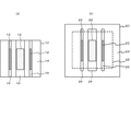
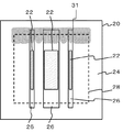
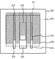
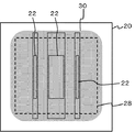
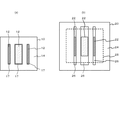
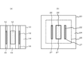
図1は、第一実施形態にかかる半導体装置の要部を示す図である。図1(a)は第1の半導体チップの接合前のバンプ形成領域近傍を拡大して示す平面図であり、図1(b)は電子部品としての第2の半導体チップの接合前のバンプ形成領域近傍を拡大して示す平面図である。
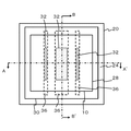
図8は、第二実施形態にかかる半導体装置の要部を示す図である。図8(a)は第1の半導体チップの接合前のバンプ形成領域近傍を拡大して示す平面図であり、図8(b)は電子部品としての第2の半導体チップの接合前のバンプ形成領域近傍を拡大して示す平面図である。
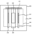
図9は、第三実施形態にかかる半導体装置の要部を示す図である。図9(a)は第1の半導体チップの接合前のバンプ形成領域近傍を拡大して示す平面図であり、図9(b)は電子部品としての第2の半導体チップの接合前のバンプ形成領域近傍を拡大して示す平面図である。
12 バンプ形成領域
13 バンプ
14 絶縁膜
16,17 開口部
20 第2の半導体チップ
22 バンプ形成領域
23 バンプ
24 絶縁膜
26.27 開口部
28 素子搭載領域
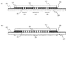
30 アンダーフィル樹脂
31 樹脂
32 バンプ形成領域
36 開口部
Claims (3)
- 表面に多行多列に配列された複数の第1のバンプを有する第1の半導体チップおよび表面に多行多列に配列された複数の第2のバンプを有する第2の半導体チップのそれぞれのバンプ形成面を対向させて形成される半導体装置において、
前記第2の半導体チップは前記第1の半導体チップよりも平面形状が大きく、
前記第1の半導体チップおよび前記第2の半導体チップのそれぞれの最表面に形成された保護膜の少なくとも一方は、平面視で前記第1の半導体チップの一部のみと重なっている開口部を有しており、
前記開口部は、平面視で、前記複数の第1のバンプ及び前記複数の第2のバンプが形成されているバンプ形成領域を内側に含んでおり、かつ前記第1の半導体チップの一方の端部から他方の端部まで延伸していることを特徴とする半導体装置。 - 請求項1に記載の半導体装置において、
前記第1の半導体チップに前記開口部が形成されている半導体装置。 - 請求項1または2に記載の半導体装置において、
前記第2の半導体チップに前記開口部が形成されており、
前記第2の半導体チップに形成された前記開口部は、平面視で前記第1の半導体チップの外側まで延伸していることを特徴とする半導体装置。
Priority Applications (2)
| Application Number | Priority Date | Filing Date | Title |
|---|---|---|---|
| JP2005082374A JP4502204B2 (ja) | 2005-03-22 | 2005-03-22 | 半導体装置 |
| US11/378,651 US7205669B2 (en) | 2005-03-22 | 2006-03-20 | Semiconductor device |
Applications Claiming Priority (1)
| Application Number | Priority Date | Filing Date | Title |
|---|---|---|---|
| JP2005082374A JP4502204B2 (ja) | 2005-03-22 | 2005-03-22 | 半導体装置 |
Publications (2)
| Publication Number | Publication Date |
|---|---|
| JP2006269541A JP2006269541A (ja) | 2006-10-05 |
| JP4502204B2 true JP4502204B2 (ja) | 2010-07-14 |
Family
ID=37034368
Family Applications (1)
| Application Number | Title | Priority Date | Filing Date |
|---|---|---|---|
| JP2005082374A Expired - Fee Related JP4502204B2 (ja) | 2005-03-22 | 2005-03-22 | 半導体装置 |
Country Status (2)
| Country | Link |
|---|---|
| US (1) | US7205669B2 (ja) |
| JP (1) | JP4502204B2 (ja) |
Families Citing this family (8)
| Publication number | Priority date | Publication date | Assignee | Title |
|---|---|---|---|---|
| US8247946B2 (en) | 2004-06-14 | 2012-08-21 | Massachusetts Institute Of Technology | Electrochemical actuator |
| US7872396B2 (en) | 2004-06-14 | 2011-01-18 | Massachusetts Institute Of Technology | Electrochemical actuator |
| US7994686B2 (en) * | 2004-06-14 | 2011-08-09 | Massachusetts Institute Of Technology | Electrochemical methods, devices, and structures |
| US7541715B2 (en) | 2004-06-14 | 2009-06-02 | Massachusetts Institute Of Technology | Electrochemical methods, devices, and structures |
| US20080124835A1 (en) * | 2006-11-03 | 2008-05-29 | International Business Machines Corporation | Hermetic seal and reliable bonding structures for 3d applications |
| JP2012119368A (ja) * | 2010-11-29 | 2012-06-21 | Elpida Memory Inc | 半導体装置の製造方法 |
| US8368285B2 (en) | 2010-12-17 | 2013-02-05 | Massachusette Institute Of Technology | Electrochemical actuators |
| JP5954075B2 (ja) * | 2012-09-21 | 2016-07-20 | ソニー株式会社 | 半導体装置及び半導体装置の製造方法 |
Family Cites Families (12)
| Publication number | Priority date | Publication date | Assignee | Title |
|---|---|---|---|---|
| JPH07112041B2 (ja) * | 1986-12-03 | 1995-11-29 | シャープ株式会社 | 半導体装置の製造方法 |
| JP2571024B2 (ja) * | 1994-09-28 | 1997-01-16 | 日本電気株式会社 | マルチチップモジュール |
| JP2825083B2 (ja) * | 1996-08-20 | 1998-11-18 | 日本電気株式会社 | 半導体素子の実装構造 |
| US5898223A (en) * | 1997-10-08 | 1999-04-27 | Lucent Technologies Inc. | Chip-on-chip IC packages |
| JPH11284032A (ja) * | 1998-03-26 | 1999-10-15 | Ricoh Co Ltd | フリップチップ接続方法とフリップチップ接続構造 |
| JP2000311921A (ja) * | 1999-04-27 | 2000-11-07 | Sony Corp | 半導体装置およびその製造方法 |
| JP3520976B2 (ja) * | 2000-01-18 | 2004-04-19 | カシオマイクロニクス株式会社 | 半導体装置の接合構造 |
| US6555917B1 (en) * | 2001-10-09 | 2003-04-29 | Amkor Technology, Inc. | Semiconductor package having stacked semiconductor chips and method of making the same |
| JP2003324182A (ja) * | 2002-04-30 | 2003-11-14 | Fujitsu Ltd | フリップチップ接合方法及びフリップチップ接合構造 |
| JP2005085931A (ja) * | 2003-09-08 | 2005-03-31 | Nec Semicon Package Solutions Ltd | 半導体チップ及びその実装回路基板 |
| TWI273664B (en) * | 2004-03-26 | 2007-02-11 | Advanced Semiconductor Eng | Bumping process, bump structure, packaging process and package structure |
| JP4971769B2 (ja) * | 2005-12-22 | 2012-07-11 | 新光電気工業株式会社 | フリップチップ実装構造及びフリップチップ実装構造の製造方法 |
-
2005
- 2005-03-22 JP JP2005082374A patent/JP4502204B2/ja not_active Expired - Fee Related
-
2006
- 2006-03-20 US US11/378,651 patent/US7205669B2/en not_active Expired - Fee Related
Also Published As
| Publication number | Publication date |
|---|---|
| US7205669B2 (en) | 2007-04-17 |
| JP2006269541A (ja) | 2006-10-05 |
| US20060214275A1 (en) | 2006-09-28 |
Similar Documents
| Publication | Publication Date | Title |
|---|---|---|
| JP3797992B2 (ja) | 半導体装置 | |
| CN108231716B (zh) | 封装结构及其制造方法 | |
| JP5993248B2 (ja) | 電子部品内蔵基板及びその製造方法 | |
| JP4441545B2 (ja) | 半導体装置 | |
| US9318460B2 (en) | Substrate and assembly thereof with dielectric removal for increased post height | |
| TWI550737B (zh) | 晶片封裝體及其製造方法 | |
| TWI575672B (zh) | 晶片封裝體及其製造方法 | |
| JP4536603B2 (ja) | 半導体装置の製造方法及び半導体装置用実装基板及び半導体装置 | |
| KR20210001929U (ko) | 칩 패키지 구조 및 그 회로 기판 | |
| JP4740765B2 (ja) | 半導体装置及びその製造方法 | |
| JP4502204B2 (ja) | 半導体装置 | |
| CN105374777A (zh) | 倒装芯片封装件及其制造方法 | |
| JP4899406B2 (ja) | フリップチップ型半導体装置 | |
| TW201719828A (zh) | 半導體裝置 | |
| JP4435187B2 (ja) | 積層型半導体装置 | |
| JP2005085931A (ja) | 半導体チップ及びその実装回路基板 | |
| JP2008300500A (ja) | 半導体装置およびその製造方法 | |
| KR100963151B1 (ko) | 반도체 패키지 몰딩용 금형 및 이를 이용한 몰딩 방법 | |
| JP4324773B2 (ja) | 半導体装置の製造方法 | |
| JP4128945B2 (ja) | 半導体装置 | |
| JP2007103733A (ja) | 基板およびそれを用いた半導体装置 | |
| JP5284125B2 (ja) | 半導体装置およびその製造方法 | |
| CN100521170C (zh) | 电路组件 | |
| JP2004228117A (ja) | 半導体装置および半導体パッケージ | |
| JP2006229018A (ja) | テープキャリア基板およびその製造方法および半導体装置 |
Legal Events
| Date | Code | Title | Description |
|---|---|---|---|
| A621 | Written request for application examination |
Free format text: JAPANESE INTERMEDIATE CODE: A621 Effective date: 20071217 |
|
| A977 | Report on retrieval |
Free format text: JAPANESE INTERMEDIATE CODE: A971007 Effective date: 20091118 |
|
| A131 | Notification of reasons for refusal |
Free format text: JAPANESE INTERMEDIATE CODE: A131 Effective date: 20091124 |
|
| A521 | Request for written amendment filed |
Free format text: JAPANESE INTERMEDIATE CODE: A523 Effective date: 20100122 |
|
| TRDD | Decision of grant or rejection written | ||
| A01 | Written decision to grant a patent or to grant a registration (utility model) |
Free format text: JAPANESE INTERMEDIATE CODE: A01 Effective date: 20100323 |
|
| A01 | Written decision to grant a patent or to grant a registration (utility model) |
Free format text: JAPANESE INTERMEDIATE CODE: A01 |
|
| A61 | First payment of annual fees (during grant procedure) |
Free format text: JAPANESE INTERMEDIATE CODE: A61 Effective date: 20100414 |
|
| R150 | Certificate of patent or registration of utility model |
Free format text: JAPANESE INTERMEDIATE CODE: R150 |
|
| FPAY | Renewal fee payment (event date is renewal date of database) |
Free format text: PAYMENT UNTIL: 20130430 Year of fee payment: 3 |
|
| FPAY | Renewal fee payment (event date is renewal date of database) |
Free format text: PAYMENT UNTIL: 20140430 Year of fee payment: 4 |
|
| S531 | Written request for registration of change of domicile |
Free format text: JAPANESE INTERMEDIATE CODE: R313531 |
|
| R350 | Written notification of registration of transfer |
Free format text: JAPANESE INTERMEDIATE CODE: R350 |
|
| LAPS | Cancellation because of no payment of annual fees |