JP4502204B2 - Semiconductor device - Google Patents
Semiconductor device Download PDFInfo
- Publication number
- JP4502204B2 JP4502204B2 JP2005082374A JP2005082374A JP4502204B2 JP 4502204 B2 JP4502204 B2 JP 4502204B2 JP 2005082374 A JP2005082374 A JP 2005082374A JP 2005082374 A JP2005082374 A JP 2005082374A JP 4502204 B2 JP4502204 B2 JP 4502204B2
- Authority
- JP
- Japan
- Prior art keywords
- semiconductor chip
- opening
- semiconductor device
- semiconductor
- bump
- Prior art date
- Legal status (The legal status is an assumption and is not a legal conclusion. Google has not performed a legal analysis and makes no representation as to the accuracy of the status listed.)
- Expired - Fee Related
Links
Images
Classifications
-
- H—ELECTRICITY
- H10—SEMICONDUCTOR DEVICES; ELECTRIC SOLID-STATE DEVICES NOT OTHERWISE PROVIDED FOR
- H10W—GENERIC PACKAGES, INTERCONNECTIONS, CONNECTORS OR OTHER CONSTRUCTIONAL DETAILS OF DEVICES COVERED BY CLASS H10
- H10W74/00—Encapsulations, e.g. protective coatings
- H10W74/01—Manufacture or treatment
- H10W74/012—Manufacture or treatment of encapsulations on active surfaces of flip-chip devices, e.g. forming underfills
-
- H—ELECTRICITY
- H10—SEMICONDUCTOR DEVICES; ELECTRIC SOLID-STATE DEVICES NOT OTHERWISE PROVIDED FOR
- H10W—GENERIC PACKAGES, INTERCONNECTIONS, CONNECTORS OR OTHER CONSTRUCTIONAL DETAILS OF DEVICES COVERED BY CLASS H10
- H10W72/00—Interconnections or connectors in packages
- H10W72/30—Die-attach connectors
-
- H—ELECTRICITY
- H10—SEMICONDUCTOR DEVICES; ELECTRIC SOLID-STATE DEVICES NOT OTHERWISE PROVIDED FOR
- H10W—GENERIC PACKAGES, INTERCONNECTIONS, CONNECTORS OR OTHER CONSTRUCTIONAL DETAILS OF DEVICES COVERED BY CLASS H10
- H10W74/00—Encapsulations, e.g. protective coatings
- H10W74/10—Encapsulations, e.g. protective coatings characterised by their shape or disposition
- H10W74/131—Encapsulations, e.g. protective coatings characterised by their shape or disposition the semiconductor body being only partially enclosed
-
- H—ELECTRICITY
- H10—SEMICONDUCTOR DEVICES; ELECTRIC SOLID-STATE DEVICES NOT OTHERWISE PROVIDED FOR
- H10W—GENERIC PACKAGES, INTERCONNECTIONS, CONNECTORS OR OTHER CONSTRUCTIONAL DETAILS OF DEVICES COVERED BY CLASS H10
- H10W74/00—Encapsulations, e.g. protective coatings
- H10W74/10—Encapsulations, e.g. protective coatings characterised by their shape or disposition
- H10W74/15—Encapsulations, e.g. protective coatings characterised by their shape or disposition on active surfaces of flip-chip devices, e.g. underfills
-
- H—ELECTRICITY
- H10—SEMICONDUCTOR DEVICES; ELECTRIC SOLID-STATE DEVICES NOT OTHERWISE PROVIDED FOR
- H10W—GENERIC PACKAGES, INTERCONNECTIONS, CONNECTORS OR OTHER CONSTRUCTIONAL DETAILS OF DEVICES COVERED BY CLASS H10
- H10W90/00—Package configurations
-
- H—ELECTRICITY
- H10—SEMICONDUCTOR DEVICES; ELECTRIC SOLID-STATE DEVICES NOT OTHERWISE PROVIDED FOR
- H10W—GENERIC PACKAGES, INTERCONNECTIONS, CONNECTORS OR OTHER CONSTRUCTIONAL DETAILS OF DEVICES COVERED BY CLASS H10
- H10W72/00—Interconnections or connectors in packages
- H10W72/071—Connecting or disconnecting
- H10W72/072—Connecting or disconnecting of bump connectors
- H10W72/07231—Techniques
- H10W72/07236—Soldering or alloying
-
- H—ELECTRICITY
- H10—SEMICONDUCTOR DEVICES; ELECTRIC SOLID-STATE DEVICES NOT OTHERWISE PROVIDED FOR
- H10W—GENERIC PACKAGES, INTERCONNECTIONS, CONNECTORS OR OTHER CONSTRUCTIONAL DETAILS OF DEVICES COVERED BY CLASS H10
- H10W72/00—Interconnections or connectors in packages
- H10W72/071—Connecting or disconnecting
- H10W72/073—Connecting or disconnecting of die-attach connectors
-
- H—ELECTRICITY
- H10—SEMICONDUCTOR DEVICES; ELECTRIC SOLID-STATE DEVICES NOT OTHERWISE PROVIDED FOR
- H10W—GENERIC PACKAGES, INTERCONNECTIONS, CONNECTORS OR OTHER CONSTRUCTIONAL DETAILS OF DEVICES COVERED BY CLASS H10
- H10W72/00—Interconnections or connectors in packages
- H10W72/851—Dispositions of multiple connectors or interconnections
- H10W72/853—On the same surface
- H10W72/856—Bump connectors and die-attach connectors
-
- H—ELECTRICITY
- H10—SEMICONDUCTOR DEVICES; ELECTRIC SOLID-STATE DEVICES NOT OTHERWISE PROVIDED FOR
- H10W—GENERIC PACKAGES, INTERCONNECTIONS, CONNECTORS OR OTHER CONSTRUCTIONAL DETAILS OF DEVICES COVERED BY CLASS H10
- H10W90/00—Package configurations
- H10W90/20—Configurations of stacked chips
- H10W90/291—Configurations of stacked chips characterised by containers, encapsulations, or other housings for the stacked chips
-
- H—ELECTRICITY
- H10—SEMICONDUCTOR DEVICES; ELECTRIC SOLID-STATE DEVICES NOT OTHERWISE PROVIDED FOR
- H10W—GENERIC PACKAGES, INTERCONNECTIONS, CONNECTORS OR OTHER CONSTRUCTIONAL DETAILS OF DEVICES COVERED BY CLASS H10
- H10W90/00—Package configurations
- H10W90/701—Package configurations characterised by the relative positions of pads or connectors relative to package parts
- H10W90/721—Package configurations characterised by the relative positions of pads or connectors relative to package parts of bump connectors
- H10W90/722—Package configurations characterised by the relative positions of pads or connectors relative to package parts of bump connectors between stacked chips
-
- H—ELECTRICITY
- H10—SEMICONDUCTOR DEVICES; ELECTRIC SOLID-STATE DEVICES NOT OTHERWISE PROVIDED FOR
- H10W—GENERIC PACKAGES, INTERCONNECTIONS, CONNECTORS OR OTHER CONSTRUCTIONAL DETAILS OF DEVICES COVERED BY CLASS H10
- H10W90/00—Package configurations
- H10W90/701—Package configurations characterised by the relative positions of pads or connectors relative to package parts
- H10W90/721—Package configurations characterised by the relative positions of pads or connectors relative to package parts of bump connectors
- H10W90/724—Package configurations characterised by the relative positions of pads or connectors relative to package parts of bump connectors between a chip and a stacked insulating package substrate, interposer or RDL
Landscapes
- Wire Bonding (AREA)
- Encapsulation Of And Coatings For Semiconductor Or Solid State Devices (AREA)
- Structures Or Materials For Encapsulating Or Coating Semiconductor Devices Or Solid State Devices (AREA)
Description
本発明は、半導体装置に関し、特に、バンプ電極によって半導体チップと半導体チップを含む電子部品とを対向させて接続し、バンプ電極部を絶縁性樹脂であるアンダーフィルによって封止する半導体装置に関する。 The present invention relates to a semiconductor device, and more particularly, to a semiconductor device in which a semiconductor chip and an electronic component including the semiconductor chip are connected to each other by bump electrodes, and a bump electrode portion is sealed with an underfill that is an insulating resin.
近年、半導体装置の高集積化、高速化に伴って、異なるチップ同士をバンプ電極によって最短距離で接続するチップオンチップ(Chip-On-Chip:以後COC)接続技術が、異なるLSIデバイス同士を、短開発期間かつ低コストで高速システム化することが可能な技術として、実用化が期待されている。 In recent years, with the higher integration and higher speed of semiconductor devices, chip-on-chip (hereinafter referred to as COC) connection technology for connecting different chips to each other with a bump electrode at the shortest distance has been achieved. Practical use is expected as a technology that enables high-speed systems with a short development period and low cost.
また、COC接続に使用されるチップにおいても、半導体装置の小型化、高機能化の需要に伴い、他の素子への接続のためのピン数の増加が要求され、このことにより狭ピッチ化、およびバンプサイズの縮小がなされている。このことは同時に、上下チップ間のギャップ、バンプ同士の隙間のサイズが小さくなる為、バンプ、チップ間に封止する絶縁性のアンダーフィル樹脂を注入する事が困難となる。また、樹脂内部に気泡(ボイド)が発生しやすく、外部へ排出され難い、などの問題も生じてくる。 Also, in chips used for COC connection, an increase in the number of pins for connection to other elements is required with the demand for miniaturization and higher functionality of semiconductor devices. And the bump size has been reduced. At the same time, since the size of the gap between the upper and lower chips and the gap between the bumps becomes small, it becomes difficult to inject an insulating underfill resin for sealing between the bump and the chip. In addition, bubbles such as voids are likely to be generated inside the resin and are difficult to be discharged to the outside.
更に、チップ表面を外部から保護する為にポリイミド(PI)などの絶縁膜を、バンプ形成部以外のエリアに形成するが、この絶縁膜により上下チップ間のギャップが小さくなってしまうことや、絶縁膜に接するアンダーフィル樹脂の流動性が低くなることにより、特に絶縁膜の段差部分でアンダーフィル樹脂の進入が止まってしまい、バンプ周囲にアンダーフィル樹脂が充填されないおそれがある。 Furthermore, in order to protect the chip surface from the outside, an insulating film such as polyimide (PI) is formed in an area other than the bump forming portion. This insulating film may reduce the gap between the upper and lower chips, Since the fluidity of the underfill resin in contact with the film is lowered, the entry of the underfill resin stops particularly at the step portion of the insulating film, and there is a possibility that the underfill resin is not filled around the bumps.
特許文献1には、互いに接続される上下チップ間にアンダーフィル樹脂が充填されるCOC構造に関し、樹脂充填時にこのアンダーフィル樹脂内にボイドが発生することを防止することを目的とした技術が開示されている。この技術によれば、通常、上下チップの間隔が小さくなると、場所によりアンダーフィル樹脂の進入速度の分布が大きくなり、特にチップ中央の領域ほど流れが遅く、外側の領域ほど流れが早くなる傾向にあるため、外側の領域を進入するアンダーフィル樹脂の中央の領域への回り込みが発生し、空気を閉じこめてしまい、ボイドが発生するおそれがあるところ、各領域での樹脂の進行速度を揃えるように調節し、ボイドの発生を防ぐことができる。
ところで、半導体装置を高度に小型化するためにさらに上下チップの間隔を小さくすると、アンダーフィル樹脂の充填の際に、バンプ形成領域周囲での樹脂の流れが特に遅くなり、バンプ形成領域周辺で気泡が混入してボイドが生じることがある。また、このバンプ形成領域周辺に生じたボイドが、信頼性を評価するための温度サイクル試験などを行う際に、膨張、収縮を繰り返してバンプ形成領域においてストレスをかけやすくなり、バンプ形成領域の部分で接合された両半導体チップ同士が外れてしまうおそれがあることが本発明者により確認された。 By the way, if the distance between the upper and lower chips is further reduced in order to make the semiconductor device highly compact, the flow of the resin around the bump forming area becomes particularly slow when filling with the underfill resin, and there is a bubble around the bump forming area. May form voids. In addition, when a void generated around the bump formation region is subjected to a temperature cycle test or the like for evaluating reliability, it becomes easy to apply stress in the bump formation region by repeatedly expanding and contracting. It has been confirmed by the present inventor that the two semiconductor chips bonded together may be detached.
この点につき、特許文献1に記載の技術では、COC構造中央の素子形成領域に閉じ込められるボイドを回避することについては一定の解決がなされているが、バンプ形成領域周辺で気泡が混入して生じるおそれのあるボイドについては何ら解決するものではなかった。
With respect to this point, in the technique described in
本発明に係る半導体装置は、表面に多行多列に配列された複数の第1のバンプを有する第1の半導体チップおよび表面に多行多列に配列された複数の第2のバンプを有する第2の半導体チップのそれぞれのバンプ形成面を対向させて形成される半導体装置において、
前記第2の半導体チップは前記第1の半導体チップよりも平面形状が大きく、
前記第1の半導体チップおよび前記第2の半導体チップのそれぞれの最表面に形成された保護膜の少なくとも一方は、平面視で前記第1の半導体チップの一部のみと重なっている開口部を有しており、
前記開口部は、平面視で、前記複数の第1のバンプ及び前記複数の第2のバンプが形成されているバンプ形成領域を内側に含んでおり、かつ前記第1の半導体チップの一方の端部から他方の端部まで延伸していることを特徴としている。
The semiconductor device according to the present invention has a first semiconductor chip having a plurality of first bumps arranged in multiple rows and multiple columns on the surface and a plurality of second bumps arranged in multiple rows and multiple columns on the surface. In the semiconductor device formed by facing the bump forming surfaces of the second semiconductor chip ,
The planar shape of the second semiconductor chip is larger than that of the first semiconductor chip,
At least one of the protective films formed on the outermost surfaces of the first semiconductor chip and the second semiconductor chip has an opening that overlaps only a part of the first semiconductor chip in plan view. And
The opening includes a bump formation region in which the plurality of first bumps and the plurality of second bumps are formed in a plan view , and one end of the first semiconductor chip. It is characterized by extending from one part to the other end .
本発明の半導体装置によれば、第1の半導体チップ、電子部品のいずれか一方の保護膜上のバンプ形成領域近傍に、第1の半導体チップおよび前記電子部品の間にアンダーフィル樹脂を流し込むための開口部を設けることによって、バンプ形成領域においてアンダーフィル樹脂が流れやすくなるので、半導体チップと電子部品との間に封止されるアンダーフィル樹脂中のボイドの発生を抑制することができる。 According to the semiconductor device of the present invention, underfill resin is poured between the first semiconductor chip and the electronic component in the vicinity of the bump forming region on the protective film of either the first semiconductor chip or the electronic component. By providing the opening, it becomes easy for the underfill resin to flow in the bump formation region, so that generation of voids in the underfill resin sealed between the semiconductor chip and the electronic component can be suppressed.
この半導体装置において、開口部を、バンプ形成領域を経由するとともに、この開口部が設けられた半導体チップまたは電子部品の一方の端部から他方の端部まで設けることができる。 In this semiconductor device, the opening can be provided from one end to the other end of the semiconductor chip or electronic component provided with the opening while passing through the bump formation region.
この構成によって、バンプ形成領域においてアンダーフィル樹脂がさらに流れやすくなるので、半導体チップと電子部品との間に封止されるアンダーフィル樹脂中のボイドがさらに発生しにくくなる。 With this configuration, the underfill resin is more likely to flow in the bump formation region, so that voids in the underfill resin sealed between the semiconductor chip and the electronic component are less likely to occur.
また、開口部を、バンプ形成領域を経由するとともに、この開口部が設けられた半導体チップまたは電子部品の相手方の一方の端部から他方の端部までの領域に対応する領域よりも大きい範囲で設けるようにしてもよく、半導体チップおよび電子部品の両方に開口部を設けてもよい。 Further, the opening passes through the bump formation region and is larger than the region corresponding to the region from one end to the other end of the semiconductor chip or electronic component provided with the opening. You may make it provide, and you may provide an opening part in both a semiconductor chip and an electronic component.
この構成によって、バンプ形成領域においてアンダーフィル樹脂がさらに流れやすくなるので、半導体チップと電子部品との間に封止されるアンダーフィル樹脂中のボイドがさらに発生しにくくなる。 With this configuration, the underfill resin is more likely to flow in the bump formation region, so that voids in the underfill resin sealed between the semiconductor chip and the electronic component are less likely to occur.
本発明によれば、バンプ電極によって接続される半導体チップおよび電子部品の間に封止されるアンダーフィル樹脂中においてボイドの発生を抑止した半導体装置を提供することができる。 ADVANTAGE OF THE INVENTION According to this invention, the semiconductor device which suppressed generation | occurrence | production of a void in the underfill resin sealed between the semiconductor chip connected by a bump electrode and an electronic component can be provided.
以下、本発明に係る半導体装置の製造方法の実施形態について、図面を参照しながら詳細に説明する。
なお、図面の説明においては、同一要素には同一符号を付し、重複する説明を省略する。
DESCRIPTION OF EMBODIMENTS Hereinafter, embodiments of a method for manufacturing a semiconductor device according to the present invention will be described in detail with reference to the drawings.
In the description of the drawings, the same reference numerals are assigned to the same elements, and duplicate descriptions are omitted.
(第一実施形態)
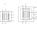
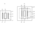
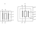
図1は、第一実施形態にかかる半導体装置の要部を示す図である。図1(a)は第1の半導体チップの接合前のバンプ形成領域近傍を拡大して示す平面図であり、図1(b)は電子部品としての第2の半導体チップの接合前のバンプ形成領域近傍を拡大して示す平面図である。
(First embodiment)
FIG. 1 is a diagram illustrating a main part of the semiconductor device according to the first embodiment. FIG. 1A is an enlarged plan view showing the vicinity of a bump formation region before bonding the first semiconductor chip, and FIG. 1B is a bump formation before bonding the second semiconductor chip as an electronic component. It is a top view which expands and shows the area | region vicinity.
本実施形態の半導体装置は、表面にバンプを有する第1の半導体チップ10および表面にバンプを有する電子部品としての第2の半導体チップ20のそれぞれのバンプ形成面を対向させて形成される半導体装置において、第1の半導体チップ10および前記電子部品のそれぞれの最表面に形成された保護膜である絶縁膜14,24の少なくとも一方の中であって、バンプ形成領域12,22の近傍に、第1の半導体チップ10と第2の半導体チップ20との間にアンダーフィル樹脂を流し込むための開口部16,26を設けたものである。
The semiconductor device of the present embodiment is formed by opposing the bump forming surfaces of the
第1の半導体チップ10および第2の半導体チップ20は、図示しないが素子形成領域(不図示)およびバンプ形成領域12,22を有し、それら領域を覆うように、層間絶縁膜(不図示)が設けられて、さらにポリイミドなどの絶縁膜14,24を設けたものである。
The
図1(a)に示したように、開口部16はバンプ形成領域12を経由するとともに、開口部16が設けられた第1の半導体チップ10の一方の端部から他方の端部まで設けられるものである。一方、図1(b)に示したように、開口部26はバンプ形成領域22を経由するとともに、開口部26が設けられた第2の半導体チップ20の相手方である第1の半導体チップ10の一方の端部から他方の端部までの領域に対応する領域よりも大きい範囲で設けられるものである。また、第1の半導体チップ10は、第2の半導体チップ20の素子搭載領域28において、互いのバンプ形成領域12,22を重ね合わせるようにして接続される。
As shown in FIG. 1A, the opening 16 passes through the
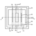
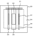
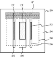
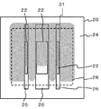
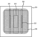
図2は、本実施形態の半導体装置において両半導体チップ同士を接続してCOC構造としたときの要部を示す平面図である。図2において、半導体装置は、第2の半導体チップ20の上の素子搭載領域28上に、バンプ形成面が対向するように、第1の半導体チップ10が搭載されており、アンダーフィル樹脂30によって封止されているバンプ形成領域32と、アンダーフィル樹脂30によって封止されている開口部36とを有している。また、図3(a)は図2のCOC構造におけるA−A’断面図であり、図3(b)は図2のCOC構造におけるB−B’断面図である。
FIG. 2 is a plan view showing the main part of the semiconductor device of this embodiment when both semiconductor chips are connected to form a COC structure. In FIG. 2, the semiconductor device has the
このCOC構造において、第1の半導体チップ10および第2の半導体チップ20の間には、アンダーフィル樹脂30が封止される。より詳細には、図3(a)および図3(b)に示したように、第1の半導体チップ10の絶縁膜14と第2の半導体チップ20の絶縁膜24との間はアンダーフィル樹脂30によって封止される。また、第1の半導体チップ10の開口部16および第2の半導体チップ20の開口部26の両方で重なることにより形成される開口部36では、前記バンプ形成領域12,22においては第1の半導体チップ10に形成されるバンプ13および第2の半導体チップ20に形成されるバンプ23が対向するとともに、バンプが形成されない部分では空間ができるため、アンダーフィル樹脂30が封止される。図3(a)において、バンプ23は、2列、3列、2列の構成で配列されているが、特にこの配列に限定されるわけではなく、必要に応じて所望の配列で構成することができる。
In this COC structure, an
ここで、バンプ同士が接続された第1の半導体チップ10および第2の半導体チップ20の間へのアンダーフィル樹脂30の封止について説明する。
Here, sealing of the
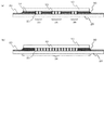
図4〜図7は、アンダーフィル樹脂が封入される様子を段階的に示す図である。なお、図中では、説明を簡略するために、第1の半導体チップ10の表記を省略して、第2の半導体チップ20の表面に樹脂を流し込むように表記するが、実際には第1の半導体チップ10側でも同様に樹脂が流れ込んでいく。
4-7 is a figure which shows a mode that underfill resin is enclosed in steps. In the figure, for the sake of simplicity, the description of the
図4では、樹脂31が素子搭載領域28の一つの端部の絶縁膜に設けられる樹脂流入部に塗布され、樹脂の導入が開始される。なお、この際、樹脂31が溶融状態になる程度に加熱することで樹脂31の流し込みが容易になる。図5では、樹脂31が毛細管現象により素子搭載領域28の反対側の端部に向かって流れ出し、絶縁膜24の表面および開口部26には樹脂31が充填していく。図6では、樹脂31はバンプ形成領域22にも流動し、さらに素子搭載領域28内の絶縁膜24および開口部26を樹脂31が充填していく。図7では、樹脂31が素子搭載領域28全体を充填して、樹脂の導入は終了し、この樹脂を加熱硬化処理することによりアンダーフィル樹脂30になる。
In FIG. 4, the
なお、樹脂31が素子搭載領域28の中を流動する際に、特にバンプ配列間隔が狭ピッチである場合に、開口部26の樹脂の進行方向の下流側に空気が残存することがあるが、開口部26の端部が素子搭載領域28の内部に埋もれているのではなく、素子搭載領域28の端部まで到達しており、第1および第2の半導体チップの接続面の端部に対して開放状態にあるため、この空気は加熱硬化処理する前に、脱法処理、例えば真空脱法処理を行うことで容易に取り除くことができる。また、図示しないが、第1の半導体チップ10の開口部16の中に空気が閉じこめられたときも同様に、この空気を加熱硬化処理前の脱法処理にて容易に取り除くことができる。
When the
上述した本実施形態の構成によって、バンプ形成領域においてアンダーフィル樹脂が流れやすくなるので、半導体チップと電子部品との間に封止されるアンダーフィル樹脂中のボイドの発生を抑制することができる。 With the configuration of the present embodiment described above, the underfill resin can easily flow in the bump formation region, so that generation of voids in the underfill resin sealed between the semiconductor chip and the electronic component can be suppressed.
(第二実施形態)
図8は、第二実施形態にかかる半導体装置の要部を示す図である。図8(a)は第1の半導体チップの接合前のバンプ形成領域近傍を拡大して示す平面図であり、図8(b)は電子部品としての第2の半導体チップの接合前のバンプ形成領域近傍を拡大して示す平面図である。
(Second embodiment)
FIG. 8 is a diagram illustrating a main part of the semiconductor device according to the second embodiment. FIG. 8A is an enlarged plan view showing the vicinity of a bump formation region before bonding the first semiconductor chip, and FIG. 8B is a bump formation before bonding the second semiconductor chip as an electronic component. It is a top view which expands and shows the area | region vicinity.
本実施形態の半導体装置では、前記第一実施形態にかかる半導体装置において、図8(a)に示した第1の半導体チップ10の絶縁膜14の中に設けられた開口部17が、バンプ形成領域12を経由して第1の半導体チップ10の端部から端部まで設けられているのではなく、バンプ形成領域12の上のみに設けられた以外は、第2の半導体チップ20などの他の構成およびアンダーフィル樹脂の封止は第一実施形態と同様である。
In the semiconductor device according to the present embodiment, in the semiconductor device according to the first embodiment, the
このように構成しても、図8(b)に示したように、第2の半導体チップ20に形成された開口部26が、バンプ形成領域22を経由するとともに、この開口部26が設けられた第2の半導体チップ20の相手方、すなわち第1の半導体チップ10の一方の端部から他方の端部よりも大きい範囲で設けられている。したがって、開口部26の端部が素子搭載領域28の内部に埋もれているのではなく、素子搭載領域28の端部まで到達しており、第一実施形態と同様に、第1および第2の半導体チップの接続面の端部に対して開放状態にあるため、開口部17,26のいずれの領域において空気が閉じこめられたとしても、この空気は加熱硬化処理する前に、脱法処理、例えば真空脱法処理を行うことで容易に取り除くことができる。また、第一実施形態の半導体装置と比べて、保護膜となる絶縁膜の開口部分が小さくなるため、保護される面積を増やすことができ、半導体装置の信頼性がさらに向上する。
Even in such a configuration, as shown in FIG. 8B, the
(第三実施形態)
図9は、第三実施形態にかかる半導体装置の要部を示す図である。図9(a)は第1の半導体チップの接合前のバンプ形成領域近傍を拡大して示す平面図であり、図9(b)は電子部品としての第2の半導体チップの接合前のバンプ形成領域近傍を拡大して示す平面図である。
(Third embodiment)
FIG. 9 is a diagram illustrating a main part of the semiconductor device according to the third embodiment. FIG. 9A is an enlarged plan view showing the vicinity of a bump formation region before bonding the first semiconductor chip, and FIG. 9B is a bump formation before bonding the second semiconductor chip as an electronic component. It is a top view which expands and shows the area | region vicinity.
本実施形態の半導体装置では、前記第一実施形態にかかる半導体装置において、図9(b)に示した第2の半導体チップ20の絶縁膜24の中に設けられた開口部27が、バンプ形成領域22を経由して、相手方である第1の半導体チップ10(図9(a))の端部から端部までより大きな幅で設けられているのではなく、バンプ形成領域22の上のみに設けられた以外は、第1の半導体チップ10などの他の構成およびアンダーフィル樹脂の封止は第一実施形態と同様である。
In the semiconductor device of this embodiment, in the semiconductor device according to the first embodiment, the
このように構成しても、第1の半導体チップ10に形成された開口部16が、バンプ形成領域12を経由するとともに、この開口部16が設けられた第1の半導体チップ10の一方の端部から他方の端部までの範囲で設けられているため、開口部16の端部が第2の半導体チップ20の素子搭載領域28の内部に埋もれているのではなく、素子搭載領域28の端部まで到達することになり、第一実施形態と同様に、第1および第2の半導体チップの接続面の端部に対して開放状態にあるため、開口部16,27のいずれの領域において空気が閉じこめられたとしても、この空気は加熱硬化処理する前に、脱法処理、例えば真空脱法処理を行うことで容易に取り除くことができる。また、第一実施形態の半導体装置と比べて、保護膜となる絶縁膜の開口部分が小さくなるため、保護される面積を増やすことができ、半導体装置の信頼性がさらに向上する。
Even in this configuration, the
本発明によれば、微細で狭ピッチなバンプ配列を持ち、均一な速度でアンダーフィル樹脂を充填することが困難なCOC構造を有する半導体装置であっても、接続する半導体チップおよび電子部品の間に封止されるアンダーフィル樹脂中においてボイドの発生を抑止した半導体装置を提供することができる。 According to the present invention, even a semiconductor device having a COC structure that has a fine and narrow pitch bump arrangement and that is difficult to fill with an underfill resin at a uniform speed can be connected between a semiconductor chip and an electronic component to be connected. It is possible to provide a semiconductor device in which the generation of voids is suppressed in the underfill resin that is sealed.
なお、前述した実施形態では、第1の半導体チップとは異なる第2の半導体チップを電子部品として含み、かつ、半導体チップ同士でCOC構造を形成する半導体装置について説明したが、これに限定されるものではなく、一方が半導体チップ以外の電子部品、例えば電極を備えたインターポーザ、回路基板などのバンプが表面に形成され、最表面に保護膜が形成されるものと、半導体チップとの積層構造で形成される半導体装置においても、同様の効果が得られる。 In the above-described embodiment, the semiconductor device including the second semiconductor chip different from the first semiconductor chip as the electronic component and forming the COC structure between the semiconductor chips has been described. However, the present invention is not limited to this. One is an electronic component other than a semiconductor chip, such as an interposer with electrodes, a bump such as a circuit board is formed on the surface, a protective film is formed on the outermost surface, and a laminated structure of the semiconductor chip The same effect can be obtained in the formed semiconductor device.
10 第1の半導体チップ
12 バンプ形成領域
13 バンプ
14 絶縁膜
16,17 開口部
20 第2の半導体チップ
22 バンプ形成領域
23 バンプ
24 絶縁膜
26.27 開口部
28 素子搭載領域
30 アンダーフィル樹脂
31 樹脂
32 バンプ形成領域
36 開口部
DESCRIPTION OF
Claims (3)
前記第2の半導体チップは前記第1の半導体チップよりも平面形状が大きく、
前記第1の半導体チップおよび前記第2の半導体チップのそれぞれの最表面に形成された保護膜の少なくとも一方は、平面視で前記第1の半導体チップの一部のみと重なっている開口部を有しており、
前記開口部は、平面視で、前記複数の第1のバンプ及び前記複数の第2のバンプが形成されているバンプ形成領域を内側に含んでおり、かつ前記第1の半導体チップの一方の端部から他方の端部まで延伸していることを特徴とする半導体装置。 Each of the first semiconductor chip having a plurality of first bumps arranged in multiple rows and multiple columns on the surface and the second semiconductor chip having a plurality of second bumps arranged in multiple rows and multiple columns on the surface In a semiconductor device formed with the bump forming surfaces facing each other,
The planar shape of the second semiconductor chip is larger than that of the first semiconductor chip,
At least one of the protective films formed on the outermost surfaces of the first semiconductor chip and the second semiconductor chip has an opening that overlaps only a part of the first semiconductor chip in plan view. And
The opening includes a bump formation region in which the plurality of first bumps and the plurality of second bumps are formed in a plan view , and one end of the first semiconductor chip. A semiconductor device characterized by extending from one end to the other end .
前記第1の半導体チップに前記開口部が形成されている半導体装置。 The semiconductor device according to claim 1,
A semiconductor device in which the opening is formed in the first semiconductor chip.
前記第2の半導体チップに前記開口部が形成されており、
前記第2の半導体チップに形成された前記開口部は、平面視で前記第1の半導体チップの外側まで延伸していることを特徴とする半導体装置。 The semiconductor device according to claim 1 or 2,
The opening is formed in the second semiconductor chip ;
The semiconductor device, wherein the opening formed in the second semiconductor chip extends to the outside of the first semiconductor chip in plan view .
Priority Applications (2)
| Application Number | Priority Date | Filing Date | Title |
|---|---|---|---|
| JP2005082374A JP4502204B2 (en) | 2005-03-22 | 2005-03-22 | Semiconductor device |
| US11/378,651 US7205669B2 (en) | 2005-03-22 | 2006-03-20 | Semiconductor device |
Applications Claiming Priority (1)
| Application Number | Priority Date | Filing Date | Title |
|---|---|---|---|
| JP2005082374A JP4502204B2 (en) | 2005-03-22 | 2005-03-22 | Semiconductor device |
Publications (2)
| Publication Number | Publication Date |
|---|---|
| JP2006269541A JP2006269541A (en) | 2006-10-05 |
| JP4502204B2 true JP4502204B2 (en) | 2010-07-14 |
Family
ID=37034368
Family Applications (1)
| Application Number | Title | Priority Date | Filing Date |
|---|---|---|---|
| JP2005082374A Expired - Fee Related JP4502204B2 (en) | 2005-03-22 | 2005-03-22 | Semiconductor device |
Country Status (2)
| Country | Link |
|---|---|
| US (1) | US7205669B2 (en) |
| JP (1) | JP4502204B2 (en) |
Families Citing this family (8)
| Publication number | Priority date | Publication date | Assignee | Title |
|---|---|---|---|---|
| US8247946B2 (en) | 2004-06-14 | 2012-08-21 | Massachusetts Institute Of Technology | Electrochemical actuator |
| US7872396B2 (en) | 2004-06-14 | 2011-01-18 | Massachusetts Institute Of Technology | Electrochemical actuator |
| US7994686B2 (en) * | 2004-06-14 | 2011-08-09 | Massachusetts Institute Of Technology | Electrochemical methods, devices, and structures |
| US7541715B2 (en) | 2004-06-14 | 2009-06-02 | Massachusetts Institute Of Technology | Electrochemical methods, devices, and structures |
| US20080124835A1 (en) * | 2006-11-03 | 2008-05-29 | International Business Machines Corporation | Hermetic seal and reliable bonding structures for 3d applications |
| JP2012119368A (en) * | 2010-11-29 | 2012-06-21 | Elpida Memory Inc | Method for manufacturing semiconductor device |
| US8368285B2 (en) | 2010-12-17 | 2013-02-05 | Massachusette Institute Of Technology | Electrochemical actuators |
| JP5954075B2 (en) * | 2012-09-21 | 2016-07-20 | ソニー株式会社 | Semiconductor device and manufacturing method of semiconductor device |
Family Cites Families (12)
| Publication number | Priority date | Publication date | Assignee | Title |
|---|---|---|---|---|
| JPH07112041B2 (en) * | 1986-12-03 | 1995-11-29 | シャープ株式会社 | Method for manufacturing semiconductor device |
| JP2571024B2 (en) * | 1994-09-28 | 1997-01-16 | 日本電気株式会社 | Multi-chip module |
| JP2825083B2 (en) * | 1996-08-20 | 1998-11-18 | 日本電気株式会社 | Semiconductor element mounting structure |
| US5898223A (en) * | 1997-10-08 | 1999-04-27 | Lucent Technologies Inc. | Chip-on-chip IC packages |
| JPH11284032A (en) * | 1998-03-26 | 1999-10-15 | Ricoh Co Ltd | Flip chip connection method and flip chip connection structure |
| JP2000311921A (en) * | 1999-04-27 | 2000-11-07 | Sony Corp | Semiconductor device and manufacturing method thereof |
| JP3520976B2 (en) * | 2000-01-18 | 2004-04-19 | カシオマイクロニクス株式会社 | Bonding structure of semiconductor device |
| US6555917B1 (en) * | 2001-10-09 | 2003-04-29 | Amkor Technology, Inc. | Semiconductor package having stacked semiconductor chips and method of making the same |
| JP2003324182A (en) * | 2002-04-30 | 2003-11-14 | Fujitsu Ltd | Flip chip bonding method and flip chip bonding structure |
| JP2005085931A (en) * | 2003-09-08 | 2005-03-31 | Nec Semicon Package Solutions Ltd | Semiconductor chip and its mounting circuit board |
| TWI273664B (en) * | 2004-03-26 | 2007-02-11 | Advanced Semiconductor Eng | Bumping process, bump structure, packaging process and package structure |
| JP4971769B2 (en) * | 2005-12-22 | 2012-07-11 | 新光電気工業株式会社 | Flip chip mounting structure and manufacturing method of flip chip mounting structure |
-
2005
- 2005-03-22 JP JP2005082374A patent/JP4502204B2/en not_active Expired - Fee Related
-
2006
- 2006-03-20 US US11/378,651 patent/US7205669B2/en not_active Expired - Fee Related
Also Published As
| Publication number | Publication date |
|---|---|
| US7205669B2 (en) | 2007-04-17 |
| JP2006269541A (en) | 2006-10-05 |
| US20060214275A1 (en) | 2006-09-28 |
Similar Documents
| Publication | Publication Date | Title |
|---|---|---|
| JP3797992B2 (en) | Semiconductor device | |
| CN108231716B (en) | Package structure and manufacturing method thereof | |
| JP5993248B2 (en) | Electronic component built-in substrate and manufacturing method thereof | |
| JP4441545B2 (en) | Semiconductor device | |
| US9318460B2 (en) | Substrate and assembly thereof with dielectric removal for increased post height | |
| TWI550737B (en) | Chip package and method of manufacturing same | |
| TWI575672B (en) | Chip package and method of manufacturing same | |
| JP4536603B2 (en) | Manufacturing method of semiconductor device, mounting substrate for semiconductor device, and semiconductor device | |
| KR20210001929U (en) | Chip package and circuit board thereof | |
| JP4740765B2 (en) | Semiconductor device and manufacturing method thereof | |
| JP4502204B2 (en) | Semiconductor device | |
| CN105374777A (en) | Flip chip package and manufacturing method thereof | |
| JP4899406B2 (en) | Flip chip type semiconductor device | |
| TW201719828A (en) | Semiconductor device | |
| JP4435187B2 (en) | Multilayer semiconductor device | |
| JP2005085931A (en) | Semiconductor chip and its mounting circuit board | |
| JP2008300500A (en) | Semiconductor device and manufacturing method thereof | |
| KR100963151B1 (en) | Mold for molding semiconductor package and molding method using the same | |
| JP4324773B2 (en) | Manufacturing method of semiconductor device | |
| JP4128945B2 (en) | Semiconductor device | |
| JP2007103733A (en) | Substrate and semiconductor device using the same | |
| JP5284125B2 (en) | Semiconductor device and manufacturing method thereof | |
| CN100521170C (en) | Circuit component | |
| JP2004228117A (en) | Semiconductor device and semiconductor package | |
| JP2006229018A (en) | Tape carrier substrate, method for manufacturing the same, and semiconductor device |
Legal Events
| Date | Code | Title | Description |
|---|---|---|---|
| A621 | Written request for application examination |
Free format text: JAPANESE INTERMEDIATE CODE: A621 Effective date: 20071217 |
|
| A977 | Report on retrieval |
Free format text: JAPANESE INTERMEDIATE CODE: A971007 Effective date: 20091118 |
|
| A131 | Notification of reasons for refusal |
Free format text: JAPANESE INTERMEDIATE CODE: A131 Effective date: 20091124 |
|
| A521 | Request for written amendment filed |
Free format text: JAPANESE INTERMEDIATE CODE: A523 Effective date: 20100122 |
|
| TRDD | Decision of grant or rejection written | ||
| A01 | Written decision to grant a patent or to grant a registration (utility model) |
Free format text: JAPANESE INTERMEDIATE CODE: A01 Effective date: 20100323 |
|
| A01 | Written decision to grant a patent or to grant a registration (utility model) |
Free format text: JAPANESE INTERMEDIATE CODE: A01 |
|
| A61 | First payment of annual fees (during grant procedure) |
Free format text: JAPANESE INTERMEDIATE CODE: A61 Effective date: 20100414 |
|
| R150 | Certificate of patent or registration of utility model |
Free format text: JAPANESE INTERMEDIATE CODE: R150 |
|
| FPAY | Renewal fee payment (event date is renewal date of database) |
Free format text: PAYMENT UNTIL: 20130430 Year of fee payment: 3 |
|
| FPAY | Renewal fee payment (event date is renewal date of database) |
Free format text: PAYMENT UNTIL: 20140430 Year of fee payment: 4 |
|
| S531 | Written request for registration of change of domicile |
Free format text: JAPANESE INTERMEDIATE CODE: R313531 |
|
| R350 | Written notification of registration of transfer |
Free format text: JAPANESE INTERMEDIATE CODE: R350 |
|
| LAPS | Cancellation because of no payment of annual fees |