JP4188337B2 - 積層型電子部品の製造方法 - Google Patents
積層型電子部品の製造方法 Download PDFInfo
- Publication number
- JP4188337B2 JP4188337B2 JP2005126443A JP2005126443A JP4188337B2 JP 4188337 B2 JP4188337 B2 JP 4188337B2 JP 2005126443 A JP2005126443 A JP 2005126443A JP 2005126443 A JP2005126443 A JP 2005126443A JP 4188337 B2 JP4188337 B2 JP 4188337B2
- Authority
- JP
- Japan
- Prior art keywords
- layer
- semiconductor element
- electronic component
- bonding
- semiconductor
- Prior art date
- Legal status (The legal status is an assumption and is not a legal conclusion. Google has not performed a legal analysis and makes no representation as to the accuracy of the status listed.)
- Expired - Fee Related
Links
Images


Classifications
-
- H—ELECTRICITY
- H01—ELECTRIC ELEMENTS
- H01L—SEMICONDUCTOR DEVICES NOT COVERED BY CLASS H10
- H01L2224/00—Indexing scheme for arrangements for connecting or disconnecting semiconductor or solid-state bodies and methods related thereto as covered by H01L24/00
- H01L2224/01—Means for bonding being attached to, or being formed on, the surface to be connected, e.g. chip-to-package, die-attach, "first-level" interconnects; Manufacturing methods related thereto
- H01L2224/26—Layer connectors, e.g. plate connectors, solder or adhesive layers; Manufacturing methods related thereto
- H01L2224/31—Structure, shape, material or disposition of the layer connectors after the connecting process
- H01L2224/32—Structure, shape, material or disposition of the layer connectors after the connecting process of an individual layer connector
- H01L2224/321—Disposition
- H01L2224/32135—Disposition the layer connector connecting between different semiconductor or solid-state bodies, i.e. chip-to-chip
- H01L2224/32145—Disposition the layer connector connecting between different semiconductor or solid-state bodies, i.e. chip-to-chip the bodies being stacked
-
- H—ELECTRICITY
- H01—ELECTRIC ELEMENTS
- H01L—SEMICONDUCTOR DEVICES NOT COVERED BY CLASS H10
- H01L2224/00—Indexing scheme for arrangements for connecting or disconnecting semiconductor or solid-state bodies and methods related thereto as covered by H01L24/00
- H01L2224/01—Means for bonding being attached to, or being formed on, the surface to be connected, e.g. chip-to-package, die-attach, "first-level" interconnects; Manufacturing methods related thereto
- H01L2224/26—Layer connectors, e.g. plate connectors, solder or adhesive layers; Manufacturing methods related thereto
- H01L2224/31—Structure, shape, material or disposition of the layer connectors after the connecting process
- H01L2224/32—Structure, shape, material or disposition of the layer connectors after the connecting process of an individual layer connector
- H01L2224/321—Disposition
- H01L2224/32151—Disposition the layer connector connecting between a semiconductor or solid-state body and an item not being a semiconductor or solid-state body, e.g. chip-to-substrate, chip-to-passive
- H01L2224/32221—Disposition the layer connector connecting between a semiconductor or solid-state body and an item not being a semiconductor or solid-state body, e.g. chip-to-substrate, chip-to-passive the body and the item being stacked
- H01L2224/32225—Disposition the layer connector connecting between a semiconductor or solid-state body and an item not being a semiconductor or solid-state body, e.g. chip-to-substrate, chip-to-passive the body and the item being stacked the item being non-metallic, e.g. insulating substrate with or without metallisation
-
- H—ELECTRICITY
- H01—ELECTRIC ELEMENTS
- H01L—SEMICONDUCTOR DEVICES NOT COVERED BY CLASS H10
- H01L2224/00—Indexing scheme for arrangements for connecting or disconnecting semiconductor or solid-state bodies and methods related thereto as covered by H01L24/00
- H01L2224/01—Means for bonding being attached to, or being formed on, the surface to be connected, e.g. chip-to-package, die-attach, "first-level" interconnects; Manufacturing methods related thereto
- H01L2224/26—Layer connectors, e.g. plate connectors, solder or adhesive layers; Manufacturing methods related thereto
- H01L2224/31—Structure, shape, material or disposition of the layer connectors after the connecting process
- H01L2224/32—Structure, shape, material or disposition of the layer connectors after the connecting process of an individual layer connector
- H01L2224/321—Disposition
- H01L2224/32151—Disposition the layer connector connecting between a semiconductor or solid-state body and an item not being a semiconductor or solid-state body, e.g. chip-to-substrate, chip-to-passive
- H01L2224/32221—Disposition the layer connector connecting between a semiconductor or solid-state body and an item not being a semiconductor or solid-state body, e.g. chip-to-substrate, chip-to-passive the body and the item being stacked
- H01L2224/32245—Disposition the layer connector connecting between a semiconductor or solid-state body and an item not being a semiconductor or solid-state body, e.g. chip-to-substrate, chip-to-passive the body and the item being stacked the item being metallic
-
- H—ELECTRICITY
- H01—ELECTRIC ELEMENTS
- H01L—SEMICONDUCTOR DEVICES NOT COVERED BY CLASS H10
- H01L2224/00—Indexing scheme for arrangements for connecting or disconnecting semiconductor or solid-state bodies and methods related thereto as covered by H01L24/00
- H01L2224/01—Means for bonding being attached to, or being formed on, the surface to be connected, e.g. chip-to-package, die-attach, "first-level" interconnects; Manufacturing methods related thereto
- H01L2224/42—Wire connectors; Manufacturing methods related thereto
- H01L2224/47—Structure, shape, material or disposition of the wire connectors after the connecting process
- H01L2224/48—Structure, shape, material or disposition of the wire connectors after the connecting process of an individual wire connector
- H01L2224/4805—Shape
- H01L2224/4809—Loop shape
- H01L2224/48091—Arched
-
- H—ELECTRICITY
- H01—ELECTRIC ELEMENTS
- H01L—SEMICONDUCTOR DEVICES NOT COVERED BY CLASS H10
- H01L2224/00—Indexing scheme for arrangements for connecting or disconnecting semiconductor or solid-state bodies and methods related thereto as covered by H01L24/00
- H01L2224/01—Means for bonding being attached to, or being formed on, the surface to be connected, e.g. chip-to-package, die-attach, "first-level" interconnects; Manufacturing methods related thereto
- H01L2224/42—Wire connectors; Manufacturing methods related thereto
- H01L2224/47—Structure, shape, material or disposition of the wire connectors after the connecting process
- H01L2224/48—Structure, shape, material or disposition of the wire connectors after the connecting process of an individual wire connector
- H01L2224/481—Disposition
- H01L2224/48151—Connecting between a semiconductor or solid-state body and an item not being a semiconductor or solid-state body, e.g. chip-to-substrate, chip-to-passive
- H01L2224/48221—Connecting between a semiconductor or solid-state body and an item not being a semiconductor or solid-state body, e.g. chip-to-substrate, chip-to-passive the body and the item being stacked
- H01L2224/48225—Connecting between a semiconductor or solid-state body and an item not being a semiconductor or solid-state body, e.g. chip-to-substrate, chip-to-passive the body and the item being stacked the item being non-metallic, e.g. insulating substrate with or without metallisation
- H01L2224/48227—Connecting between a semiconductor or solid-state body and an item not being a semiconductor or solid-state body, e.g. chip-to-substrate, chip-to-passive the body and the item being stacked the item being non-metallic, e.g. insulating substrate with or without metallisation connecting the wire to a bond pad of the item
-
- H—ELECTRICITY
- H01—ELECTRIC ELEMENTS
- H01L—SEMICONDUCTOR DEVICES NOT COVERED BY CLASS H10
- H01L2224/00—Indexing scheme for arrangements for connecting or disconnecting semiconductor or solid-state bodies and methods related thereto as covered by H01L24/00
- H01L2224/73—Means for bonding being of different types provided for in two or more of groups H01L2224/10, H01L2224/18, H01L2224/26, H01L2224/34, H01L2224/42, H01L2224/50, H01L2224/63, H01L2224/71
- H01L2224/732—Location after the connecting process
- H01L2224/73251—Location after the connecting process on different surfaces
- H01L2224/73265—Layer and wire connectors
-
- H—ELECTRICITY
- H01—ELECTRIC ELEMENTS
- H01L—SEMICONDUCTOR DEVICES NOT COVERED BY CLASS H10
- H01L24/00—Arrangements for connecting or disconnecting semiconductor or solid-state bodies; Methods or apparatus related thereto
- H01L24/73—Means for bonding being of different types provided for in two or more of groups H01L24/10, H01L24/18, H01L24/26, H01L24/34, H01L24/42, H01L24/50, H01L24/63, H01L24/71
-
- H—ELECTRICITY
- H01—ELECTRIC ELEMENTS
- H01L—SEMICONDUCTOR DEVICES NOT COVERED BY CLASS H10
- H01L2924/00—Indexing scheme for arrangements or methods for connecting or disconnecting semiconductor or solid-state bodies as covered by H01L24/00
- H01L2924/095—Indexing scheme for arrangements or methods for connecting or disconnecting semiconductor or solid-state bodies as covered by H01L24/00 with a principal constituent of the material being a combination of two or more materials provided in the groups H01L2924/013 - H01L2924/0715
- H01L2924/097—Glass-ceramics, e.g. devitrified glass
- H01L2924/09701—Low temperature co-fired ceramic [LTCC]
-
- H—ELECTRICITY
- H01—ELECTRIC ELEMENTS
- H01L—SEMICONDUCTOR DEVICES NOT COVERED BY CLASS H10
- H01L2924/00—Indexing scheme for arrangements or methods for connecting or disconnecting semiconductor or solid-state bodies as covered by H01L24/00
- H01L2924/15—Details of package parts other than the semiconductor or other solid state devices to be connected
- H01L2924/151—Die mounting substrate
- H01L2924/153—Connection portion
- H01L2924/1531—Connection portion the connection portion being formed only on the surface of the substrate opposite to the die mounting surface
- H01L2924/15311—Connection portion the connection portion being formed only on the surface of the substrate opposite to the die mounting surface being a ball array, e.g. BGA
-
- H—ELECTRICITY
- H01—ELECTRIC ELEMENTS
- H01L—SEMICONDUCTOR DEVICES NOT COVERED BY CLASS H10
- H01L2924/00—Indexing scheme for arrangements or methods for connecting or disconnecting semiconductor or solid-state bodies as covered by H01L24/00
- H01L2924/19—Details of hybrid assemblies other than the semiconductor or other solid state devices to be connected
- H01L2924/191—Disposition
- H01L2924/19101—Disposition of discrete passive components
- H01L2924/19107—Disposition of discrete passive components off-chip wires
Description
Claims (4)
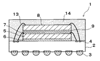
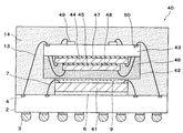
- 電極部を有する基板上に第1の電極パッドを有する第1の電子部品を接着する工程と、
前記電極部と前記第1の電極パッドとを、第1のボンディングワイヤを介して接続する工程と、
前記第1の電子部品上に、第2の電極パッドを有する第2の電子部品を、同一組成の熱硬化性樹脂で形成された2層構造の接着剤層を用いて接着する工程と、
前記電極部と前記第2の電極パッドとを、第2のボンディングワイヤを介して接続する工程とを具備し、
前記2層構造の接着剤層は、前記第1の電子部品側に配置され、前記第2の電子部品の接着時温度で軟化または溶融する半硬化状態の第1の層と、前記第2の電子部品側に配置され、前記第1の層より大きい弾性率を有すると共に、前記第2の電子部品の接着時温度に対して層形状が維持される半硬化状態の第2の層とを備え、
前記第2の電子部品の接着時に、前記第1のボンディングワイヤを前記第1の層を硬化させた硬化樹脂層内に取り込みつつ、前記第2の層を硬化させた硬化樹脂層により前記第2の電子部品から離間させることを特徴とする積層型電子部品の製造方法。 - 請求項1記載の積層型電子部品の製造方法において、
前記第1の層は前記接着時温度における粘度が1kPa・s以上100kPa・s以下であり、かつ前記第2の層は前記接着時温度における粘度が130kPa・s以上1000kPa・s以下であることを特徴とする積層型電子部品の製造方法。 - 請求項1または請求項2記載の積層型電子部品の製造方法において、
支持体上または前記第2の半導体素子の裏面に熱硬化性樹脂ワニスを塗布し乾燥させて前記第2の層を形成する工程と、前記第2の層と同一の熱硬化性樹脂ワニスを前記第2の層上に塗布し、前記第2の層を形成する際の乾燥温度より低い温度または乾燥時間より短い時間で乾燥させて前記第1の層を形成する工程とを有することを特徴とする積層型電子部品の製造方法。 - 請求項3記載の積層型電子部品の製造方法において、
前記支持体上に形成した前記第2の層と前記第1の層とを有する接着剤フィルムを、前記第2の半導体素子の裏面、または前記第2の半導体素子に個片化する前の半導体ウエハに貼り付ける工程を有することを特徴とする積層型電子部品の製造方法。
Priority Applications (1)
| Application Number | Priority Date | Filing Date | Title |
|---|---|---|---|
| JP2005126443A JP4188337B2 (ja) | 2004-05-20 | 2005-04-25 | 積層型電子部品の製造方法 |
Applications Claiming Priority (3)
| Application Number | Priority Date | Filing Date | Title |
|---|---|---|---|
| JP2004150046 | 2004-05-20 | ||
| JP2004150047 | 2004-05-20 | ||
| JP2005126443A JP4188337B2 (ja) | 2004-05-20 | 2005-04-25 | 積層型電子部品の製造方法 |
Related Child Applications (1)
| Application Number | Title | Priority Date | Filing Date |
|---|---|---|---|
| JP2008117005A Division JP4746646B2 (ja) | 2004-05-20 | 2008-04-28 | 積層型電子部品 |
Publications (3)
| Publication Number | Publication Date |
|---|---|
| JP2006005333A JP2006005333A (ja) | 2006-01-05 |
| JP2006005333A5 JP2006005333A5 (ja) | 2006-09-14 |
| JP4188337B2 true JP4188337B2 (ja) | 2008-11-26 |
Family
ID=35773403
Family Applications (1)
| Application Number | Title | Priority Date | Filing Date |
|---|---|---|---|
| JP2005126443A Expired - Fee Related JP4188337B2 (ja) | 2004-05-20 | 2005-04-25 | 積層型電子部品の製造方法 |
Country Status (1)
| Country | Link |
|---|---|
| JP (1) | JP4188337B2 (ja) |
Families Citing this family (32)
| Publication number | Priority date | Publication date | Assignee | Title |
|---|---|---|---|---|
| JP4871280B2 (ja) * | 2005-08-30 | 2012-02-08 | スパンション エルエルシー | 半導体装置およびその製造方法 |
| JP4621595B2 (ja) * | 2006-01-11 | 2011-01-26 | 株式会社東芝 | 半導体装置の製造方法 |
| JP2007242684A (ja) * | 2006-03-06 | 2007-09-20 | Disco Abrasive Syst Ltd | 積層型半導体装置及びデバイスの積層方法 |
| JP4881044B2 (ja) * | 2006-03-16 | 2012-02-22 | 株式会社東芝 | 積層型半導体装置の製造方法 |
| JP5207336B2 (ja) * | 2006-06-05 | 2013-06-12 | ルネサスエレクトロニクス株式会社 | 半導体装置 |
| TWI429054B (zh) | 2006-06-12 | 2014-03-01 | Stats Chippac Ltd | 具有偏置堆疊之積體電路封裝系統 |
| JP5166716B2 (ja) * | 2006-09-26 | 2013-03-21 | 積水化学工業株式会社 | 半導体チップ積層体及びその製造方法 |
| KR100837000B1 (ko) | 2007-05-22 | 2008-06-10 | 엘에스전선 주식회사 | 와이어 침투 다이 접착 필름 |
| JP5529371B2 (ja) * | 2007-10-16 | 2014-06-25 | ピーエスフォー ルクスコ エスエイアールエル | 半導体装置及びその製造方法 |
| JP2010040835A (ja) | 2008-08-06 | 2010-02-18 | Toshiba Corp | 積層型半導体装置の製造方法 |
| JP5595314B2 (ja) * | 2011-03-22 | 2014-09-24 | ルネサスエレクトロニクス株式会社 | 半導体装置 |
| JP5673423B2 (ja) * | 2011-08-03 | 2015-02-18 | 富士通セミコンダクター株式会社 | 半導体装置および半導体装置の製造方法 |
| JP5571045B2 (ja) * | 2011-08-19 | 2014-08-13 | 株式会社東芝 | 積層型半導体装置 |
| JP2013098240A (ja) * | 2011-10-28 | 2013-05-20 | Toshiba Corp | 記憶装置、半導体装置及び半導体装置の製造方法 |
| JP5840479B2 (ja) * | 2011-12-20 | 2016-01-06 | 株式会社東芝 | 半導体装置およびその製造方法 |
| JP5918664B2 (ja) * | 2012-09-10 | 2016-05-18 | 株式会社東芝 | 積層型半導体装置の製造方法 |
| JP5853944B2 (ja) * | 2012-12-25 | 2016-02-09 | 住友ベークライト株式会社 | 半導体装置の製造方法 |
| JP6101492B2 (ja) * | 2013-01-10 | 2017-03-22 | 日東電工株式会社 | 接着フィルム、ダイシング・ダイボンドフィルム、半導体装置の製造方法及び半導体装置 |
| JP5814965B2 (ja) * | 2013-03-15 | 2015-11-17 | 株式会社東芝 | 半導体装置 |
| JP2014216488A (ja) * | 2013-04-25 | 2014-11-17 | 日東電工株式会社 | 接着フィルム、ダイシング・ダイボンドフィルム、半導体装置の製造方法及び半導体装置 |
| KR102191823B1 (ko) * | 2013-12-27 | 2020-12-16 | 엘지디스플레이 주식회사 | 유기발광다이오드 표시장치 및 이의 제조방법 |
| JP6373811B2 (ja) * | 2015-09-08 | 2018-08-15 | 東芝メモリ株式会社 | 半導体装置の製造方法および製造装置 |
| SG11202004664PA (en) * | 2018-01-30 | 2020-06-29 | Hitachi Chemical Co Ltd | Semiconductor device production method and film-shaped adhesive |
| JP7247733B2 (ja) * | 2019-04-25 | 2023-03-29 | 株式会社レゾナック | ドルメン構造を有する半導体装置の製造方法 |
| WO2020217397A1 (ja) | 2019-04-25 | 2020-10-29 | 日立化成株式会社 | ドルメン構造を有する半導体装置の製造方法、支持片の製造方法及び積層フィルム |
| WO2020217394A1 (ja) * | 2019-04-25 | 2020-10-29 | 日立化成株式会社 | ドルメン構造を有する半導体装置及びその製造方法、並びに、支持片形成用積層フィルム及びその製造方法 |
| KR20210146908A (ko) * | 2019-04-25 | 2021-12-06 | 쇼와덴코머티리얼즈가부시끼가이샤 | 돌멘 구조를 갖는 반도체 장치의 제조 방법, 지지편의 제조 방법, 및 지지편 형성용 적층 필름 |
| WO2020217411A1 (ja) * | 2019-04-25 | 2020-10-29 | 日立化成株式会社 | ドルメン構造を有する半導体装置及びその製造方法、並びに、支持片形成用積層フィルム及びその製造方法 |
| US20220157802A1 (en) * | 2019-04-25 | 2022-05-19 | Showa Denko Materials Co., Ltd. | Semiconductor device having dolmen structure and method for manufacturing same |
| WO2020217401A1 (ja) * | 2019-04-25 | 2020-10-29 | 日立化成株式会社 | ドルメン構造を有する半導体装置及びその製造方法、並びに、支持片形成用積層フィルム及びその製造方法 |
| CN113632225A (zh) * | 2019-04-25 | 2021-11-09 | 昭和电工材料株式会社 | 具有支石墓结构的半导体装置及其制造方法、支撑片的制造方法、以及支撑片形成用层叠膜 |
| CN114270481A (zh) | 2019-08-29 | 2022-04-01 | 昭和电工材料株式会社 | 支撑片的制造方法、半导体装置的制造方法及支撑片形成用层叠膜 |
-
2005
- 2005-04-25 JP JP2005126443A patent/JP4188337B2/ja not_active Expired - Fee Related
Also Published As
| Publication number | Publication date |
|---|---|
| JP2006005333A (ja) | 2006-01-05 |
Similar Documents
| Publication | Publication Date | Title |
|---|---|---|
| JP4188337B2 (ja) | 積層型電子部品の製造方法 | |
| JP4746646B2 (ja) | 積層型電子部品 | |
| US7785926B2 (en) | Method of manufacturing stack-type semiconductor device and method of manufacturing stack-type electronic component | |
| US20050205981A1 (en) | Stacked electronic part | |
| JP2007250887A (ja) | 積層型半導体装置 | |
| US8093104B1 (en) | Multi-chip stacking method to reduce voids between stacked chips | |
| JP4203031B2 (ja) | 積層型電子部品の製造方法 | |
| JP2003078105A (ja) | スタックチップモジュール | |
| JP5673423B2 (ja) | 半導体装置および半導体装置の製造方法 | |
| JP2010010301A (ja) | 半導体装置及びその製造方法 | |
| JP2010040835A (ja) | 積層型半導体装置の製造方法 | |
| JP2012216644A (ja) | 半導体装置及びその製造方法 | |
| JP4594777B2 (ja) | 積層型電子部品の製造方法 | |
| JP2007035865A (ja) | 半導体パッケージとその製造方法 | |
| CN101295710B (zh) | 半导体器件 | |
| JP4621595B2 (ja) | 半導体装置の製造方法 | |
| JP2012009655A (ja) | 半導体パッケージおよび半導体パッケージの製造方法 | |
| JP2007242684A (ja) | 積層型半導体装置及びデバイスの積層方法 | |
| JP2007035864A (ja) | 半導体パッケージ | |
| KR101078359B1 (ko) | 반도체 디바이스 및 그 제조 방법 | |
| JP2007324443A (ja) | 積層型半導体装置とその製造方法 | |
| JP2007081127A (ja) | 半導体装置及び半導体装置の製造方法 | |
| JP2008282941A (ja) | 半導体装置 | |
| JP2005129897A (ja) | 半導体装置およびその製造方法 | |
| JP2005191398A (ja) | 半導体実装体及びその製造方法 |
Legal Events
| Date | Code | Title | Description |
|---|---|---|---|
| A521 | Request for written amendment filed |
Free format text: JAPANESE INTERMEDIATE CODE: A523 Effective date: 20060731 |
|
| A621 | Written request for application examination |
Free format text: JAPANESE INTERMEDIATE CODE: A621 Effective date: 20060731 |
|
| A977 | Report on retrieval |
Free format text: JAPANESE INTERMEDIATE CODE: A971007 Effective date: 20080218 |
|
| A131 | Notification of reasons for refusal |
Free format text: JAPANESE INTERMEDIATE CODE: A131 Effective date: 20080226 |
|
| A521 | Request for written amendment filed |
Free format text: JAPANESE INTERMEDIATE CODE: A523 Effective date: 20080428 |
|
| A02 | Decision of refusal |
Free format text: JAPANESE INTERMEDIATE CODE: A02 Effective date: 20080610 |
|
| A521 | Request for written amendment filed |
Free format text: JAPANESE INTERMEDIATE CODE: A523 Effective date: 20080630 |
|
| A911 | Transfer to examiner for re-examination before appeal (zenchi) |
Free format text: JAPANESE INTERMEDIATE CODE: A911 Effective date: 20080808 |
|
| TRDD | Decision of grant or rejection written | ||
| A01 | Written decision to grant a patent or to grant a registration (utility model) |
Free format text: JAPANESE INTERMEDIATE CODE: A01 Effective date: 20080909 |
|
| A01 | Written decision to grant a patent or to grant a registration (utility model) |
Free format text: JAPANESE INTERMEDIATE CODE: A01 |
|
| A61 | First payment of annual fees (during grant procedure) |
Free format text: JAPANESE INTERMEDIATE CODE: A61 Effective date: 20080910 |
|
| R151 | Written notification of patent or utility model registration |
Ref document number: 4188337 Country of ref document: JP Free format text: JAPANESE INTERMEDIATE CODE: R151 |
|
| FPAY | Renewal fee payment (event date is renewal date of database) |
Free format text: PAYMENT UNTIL: 20110919 Year of fee payment: 3 |
|
| FPAY | Renewal fee payment (event date is renewal date of database) |
Free format text: PAYMENT UNTIL: 20110919 Year of fee payment: 3 |
|
| FPAY | Renewal fee payment (event date is renewal date of database) |
Free format text: PAYMENT UNTIL: 20120919 Year of fee payment: 4 |
|
| FPAY | Renewal fee payment (event date is renewal date of database) |
Free format text: PAYMENT UNTIL: 20120919 Year of fee payment: 4 |
|
| FPAY | Renewal fee payment (event date is renewal date of database) |
Free format text: PAYMENT UNTIL: 20130919 Year of fee payment: 5 |
|
| S111 | Request for change of ownership or part of ownership |
Free format text: JAPANESE INTERMEDIATE CODE: R313111 |
|
| R350 | Written notification of registration of transfer |
Free format text: JAPANESE INTERMEDIATE CODE: R350 |
|
| S111 | Request for change of ownership or part of ownership |
Free format text: JAPANESE INTERMEDIATE CODE: R313111 |
|
| R350 | Written notification of registration of transfer |
Free format text: JAPANESE INTERMEDIATE CODE: R350 |
|
| LAPS | Cancellation because of no payment of annual fees |