JP4144591B2 - 半導体装置 - Google Patents
半導体装置 Download PDFInfo
- Publication number
- JP4144591B2 JP4144591B2 JP2004351183A JP2004351183A JP4144591B2 JP 4144591 B2 JP4144591 B2 JP 4144591B2 JP 2004351183 A JP2004351183 A JP 2004351183A JP 2004351183 A JP2004351183 A JP 2004351183A JP 4144591 B2 JP4144591 B2 JP 4144591B2
- Authority
- JP
- Japan
- Prior art keywords
- pad
- resistor
- power
- wiring
- semiconductor device
- Prior art date
- Legal status (The legal status is an assumption and is not a legal conclusion. Google has not performed a legal analysis and makes no representation as to the accuracy of the status listed.)
- Expired - Fee Related
Links
Images


Classifications
-
- H—ELECTRICITY
- H10—SEMICONDUCTOR DEVICES; ELECTRIC SOLID-STATE DEVICES NOT OTHERWISE PROVIDED FOR
- H10W—GENERIC PACKAGES, INTERCONNECTIONS, CONNECTORS OR OTHER CONSTRUCTIONAL DETAILS OF DEVICES COVERED BY CLASS H10
- H10W72/00—Interconnections or connectors in packages
- H10W72/90—Bond pads, in general
-
- H—ELECTRICITY
- H10—SEMICONDUCTOR DEVICES; ELECTRIC SOLID-STATE DEVICES NOT OTHERWISE PROVIDED FOR
- H10W—GENERIC PACKAGES, INTERCONNECTIONS, CONNECTORS OR OTHER CONSTRUCTIONAL DETAILS OF DEVICES COVERED BY CLASS H10
- H10W72/00—Interconnections or connectors in packages
- H10W72/50—Bond wires
- H10W72/541—Dispositions of bond wires
- H10W72/547—Dispositions of multiple bond wires
- H10W72/5473—Dispositions of multiple bond wires multiple bond wires connected to a common bond pad
-
- H—ELECTRICITY
- H10—SEMICONDUCTOR DEVICES; ELECTRIC SOLID-STATE DEVICES NOT OTHERWISE PROVIDED FOR
- H10W—GENERIC PACKAGES, INTERCONNECTIONS, CONNECTORS OR OTHER CONSTRUCTIONAL DETAILS OF DEVICES COVERED BY CLASS H10
- H10W72/00—Interconnections or connectors in packages
- H10W72/90—Bond pads, in general
- H10W72/931—Shapes of bond pads
- H10W72/932—Plan-view shape, i.e. in top view
Landscapes
- Semiconductor Integrated Circuits (AREA)
- Metal-Oxide And Bipolar Metal-Oxide Semiconductor Integrated Circuits (AREA)
Description
本発明は上記事情に鑑みてなされたもので、その目的は、電流検出用の抵抗が形成されたICチップを有する半導体装置を提供することにある。
以下、本発明の第1の実施形態について図1ないし図3を参照しながら説明する。
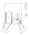
図1は、ICチップの素子配置およびICチップとリードフレームの端子との接続態様を示しており、図2は、当該ICチップに搭載された回路と外部に接続される回路の電気的構成を示している。これら図1、図2において、従来技術を示す図6、図7と同一部分には同一符号を付して示している。
図2において、IC21をハイサイドスイッチとして用いる場合、制御回路3は、図示しないチャージポンプ回路の出力電圧を用いて、MOSFET2のゲートに駆動電圧を与える。MOSFET2がオンすると、電源13から端子7、MOSFET2、シャント抵抗23、端子12、ソレノイド15の経路で主回路電流が流れ、MOSFET2がオフすると、還流ダイオード14、端子8、シャント抵抗23、端子12、ソレノイド15の経路で還流電流が流れる。制御回路3は、シャント抵抗23から配線27、28によって取り出される電圧に基づいて、ソレノイド15に流れる電流を制御する。
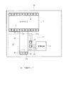
図4は、本発明の第2の実施形態におけるICチップの素子配置を示している。
ICチップ38(半導体チップに相当)は、第1の実施形態で説明したICチップ22に対しシャント抵抗23の配置が異なっている。すなわち、シャント抵抗23は、その幅の中心線とMOSFET2のパッド列の中央位置とが一致するように形成されている。
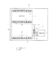
図5は、本発明の第2の実施形態におけるICチップの素子配置を示している。
ICチップ39(半導体チップに相当)において、シャント抵抗40は、MOSFET2のパッド列長に等しい幅を有し、当該シャント抵抗40とパッド列とがその全幅において相対するように形成されている。このような配置によれば、MOSFET2からシャント抵抗40に流れ込む電流およびパッド5からシャント抵抗40に流れ込む還流電流は、MOSFET2の内部およびシャント抵抗40の内部を均一に流れる。従って、より一層発熱の増加を抑えられるとともに高い電流検出精度を確保できる。
なお、本発明は上記し且つ図面に示す各実施形態に限定されるものではなく、例えば以下のように変形または拡張が可能である。
シャント抵抗23、40は、その電流通過方向に沿った辺がMOSFET2のパッド列に直交する向きとなることが最も好ましい配置であるが、正確に直交する向きでなくても上述した効果を得ることができる。
シャント抵抗23、40と配線27、28とを接続するビア25、26は、それぞれ複数設けてもよい。
シャント抵抗23、40は、アルミニウムに限らず他の金属材料や半導体材料を用いて構成してもよい。
Claims (6)
- 同一の半導体基板にパワー素子、当該パワー素子の主端子に接続される電流検出用の抵抗および前記パワー素子を制御する制御回路が形成された半導体チップを備え、
前記パワー素子の主端子のパッドは、当該パワー素子の素子形成領域の辺部に沿って列状に形成されており、
前記抵抗は、その電流通過方向に沿った辺が前記パワー素子のパッド列に直交する向きとなるように前記パワー素子に隣接して形成されていることを特徴とする半導体装置。 - 前記抵抗は、前記パワー素子の主端子のパッド列長に等しい幅を有し、当該抵抗の一端と前記パッド列とがその全幅において隣接するように形成されていることを特徴とする請求項1記載の半導体装置。
- 前記列状に形成されたパッドのうち等間隔に選択された複数のパッドと前記半導体チップの外部との間で配線がなされていることを特徴とする請求項2記載の半導体装置。
- 前記抵抗は、その幅の中心線と前記パワー素子のパッド列の中央位置とが一致するように形成されていることを特徴とする請求項1記載の半導体装置。
- 前記パワー素子の列状に形成された主端子のパッドのうち前記抵抗と隣接する位置に形成されたパッドと前記半導体チップの外部との間で配線がなされていることを特徴とする請求項1または4記載の半導体装置。
- 前記抵抗においてその電流通過方向に所定間隔を隔てた位置から前記制御回路に至る一対の引き出し用配線が形成され、
その引き出し用配線の少なくとも一方は、前記抵抗から第1のパッドに至る第1の配線と、前記第1のパッドと絶縁された第2のパッドから前記制御回路に至る第2の配線とから構成されていることを特徴とする請求項1ないし5の何れかに記載の半導体装置。
Priority Applications (1)
| Application Number | Priority Date | Filing Date | Title |
|---|---|---|---|
| JP2004351183A JP4144591B2 (ja) | 2004-12-03 | 2004-12-03 | 半導体装置 |
Applications Claiming Priority (1)
| Application Number | Priority Date | Filing Date | Title |
|---|---|---|---|
| JP2004351183A JP4144591B2 (ja) | 2004-12-03 | 2004-12-03 | 半導体装置 |
Publications (2)
| Publication Number | Publication Date |
|---|---|
| JP2006165100A JP2006165100A (ja) | 2006-06-22 |
| JP4144591B2 true JP4144591B2 (ja) | 2008-09-03 |
Family
ID=36666789
Family Applications (1)
| Application Number | Title | Priority Date | Filing Date |
|---|---|---|---|
| JP2004351183A Expired - Fee Related JP4144591B2 (ja) | 2004-12-03 | 2004-12-03 | 半導体装置 |
Country Status (1)
| Country | Link |
|---|---|
| JP (1) | JP4144591B2 (ja) |
Families Citing this family (9)
| Publication number | Priority date | Publication date | Assignee | Title |
|---|---|---|---|---|
| JP5194585B2 (ja) * | 2007-06-29 | 2013-05-08 | 富士電機株式会社 | 半導体装置の試験方法 |
| JP4513920B2 (ja) * | 2008-06-19 | 2010-07-28 | 株式会社デンソー | 定電流制御回路 |
| JP2011069809A (ja) * | 2009-08-31 | 2011-04-07 | Hitachi Automotive Systems Ltd | 制御システム及びそれに用いる半導体素子 |
| JP5280332B2 (ja) | 2009-10-30 | 2013-09-04 | 日立オートモティブシステムズ株式会社 | 電流制御用半導体素子およびそれを用いた制御装置 |
| JP5406145B2 (ja) | 2010-08-31 | 2014-02-05 | 日立オートモティブシステムズ株式会社 | 電流制御用半導体素子、およびそれを用いた制御装置 |
| JP5395127B2 (ja) | 2011-07-14 | 2014-01-22 | 日立オートモティブシステムズ株式会社 | 電流制御用半導体素子およびそれを用いた制御装置 |
| JP6541223B2 (ja) * | 2015-01-16 | 2019-07-10 | 新日本無線株式会社 | 半導体装置 |
| JP6957892B2 (ja) * | 2016-08-02 | 2021-11-02 | 富士電機株式会社 | 半導体装置およびその特性評価方法 |
| DE102018207308B4 (de) * | 2018-05-09 | 2020-07-02 | Infineon Technologies Ag | Halbleiterbauteil mit integriertem shunt-widerstand und verfahren zu dessen herstellung |
-
2004
- 2004-12-03 JP JP2004351183A patent/JP4144591B2/ja not_active Expired - Fee Related
Also Published As
| Publication number | Publication date |
|---|---|
| JP2006165100A (ja) | 2006-06-22 |
Similar Documents
| Publication | Publication Date | Title |
|---|---|---|
| US20230317713A1 (en) | Semiconductor Device | |
| JP4807768B2 (ja) | パワートランジスタ装置及びそれを用いたパワー制御システム | |
| JP5526849B2 (ja) | 半導体装置 | |
| CN106558583A (zh) | 半导体装置 | |
| US6529062B2 (en) | Power module | |
| CN101276811A (zh) | 半导体器件 | |
| JP4144591B2 (ja) | 半導体装置 | |
| JP2008533734A (ja) | 温度感知機能を有するmosfet | |
| TW201532162A (zh) | 半導體積體電路裝置 | |
| JPH09283632A (ja) | 半導体集積回路装置 | |
| KR100194312B1 (ko) | 정전 파괴 보호 회로를 구비한 반도체 디바이스 | |
| JP7090044B2 (ja) | 半導体装置 | |
| CN116298456A (zh) | 电流测量电路 | |
| JPS63141357A (ja) | パワーmosfet | |
| JP6890480B2 (ja) | 半導体装置 | |
| US7122882B2 (en) | Low cost power MOSFET with current monitoring | |
| JPH11121683A (ja) | 半導体集積回路 | |
| US7714363B2 (en) | Semiconductor integrated circuit for driving the address of a display device | |
| JP3383451B2 (ja) | 半導体装置 | |
| JP2570990B2 (ja) | 半導体集積回路 | |
| JP2676801B2 (ja) | 出力バッファ回路を備えた半導体集積回路装置 | |
| CN104247027A (zh) | 功率晶体管模块 | |
| JP2001156178A (ja) | 半導体装置および半導体装置の自動レイアウト方法 | |
| US7719254B2 (en) | Method for setting a reference potential of a current sensor and arrangement for determining the reference potential of a power semiconductor device | |
| JP7707658B2 (ja) | 集積回路装置 |
Legal Events
| Date | Code | Title | Description |
|---|---|---|---|
| A977 | Report on retrieval |
Free format text: JAPANESE INTERMEDIATE CODE: A971007 Effective date: 20071220 |
|
| A131 | Notification of reasons for refusal |
Free format text: JAPANESE INTERMEDIATE CODE: A131 Effective date: 20080408 |
|
| A521 | Request for written amendment filed |
Free format text: JAPANESE INTERMEDIATE CODE: A523 Effective date: 20080425 |
|
| TRDD | Decision of grant or rejection written | ||
| A01 | Written decision to grant a patent or to grant a registration (utility model) |
Free format text: JAPANESE INTERMEDIATE CODE: A01 Effective date: 20080527 |
|
| A01 | Written decision to grant a patent or to grant a registration (utility model) |
Free format text: JAPANESE INTERMEDIATE CODE: A01 |
|
| A61 | First payment of annual fees (during grant procedure) |
Free format text: JAPANESE INTERMEDIATE CODE: A61 Effective date: 20080609 |
|
| R150 | Certificate of patent or registration of utility model |
Free format text: JAPANESE INTERMEDIATE CODE: R150 |
|
| FPAY | Renewal fee payment (event date is renewal date of database) |
Free format text: PAYMENT UNTIL: 20110627 Year of fee payment: 3 |
|
| FPAY | Renewal fee payment (event date is renewal date of database) |
Free format text: PAYMENT UNTIL: 20110627 Year of fee payment: 3 |
|
| FPAY | Renewal fee payment (event date is renewal date of database) |
Free format text: PAYMENT UNTIL: 20120627 Year of fee payment: 4 |
|
| FPAY | Renewal fee payment (event date is renewal date of database) |
Free format text: PAYMENT UNTIL: 20120627 Year of fee payment: 4 |
|
| FPAY | Renewal fee payment (event date is renewal date of database) |
Free format text: PAYMENT UNTIL: 20130627 Year of fee payment: 5 |
|
| FPAY | Renewal fee payment (event date is renewal date of database) |
Free format text: PAYMENT UNTIL: 20140627 Year of fee payment: 6 |
|
| R250 | Receipt of annual fees |
Free format text: JAPANESE INTERMEDIATE CODE: R250 |
|
| LAPS | Cancellation because of no payment of annual fees |