JP4144591B2 - Semiconductor device - Google Patents
Semiconductor device Download PDFInfo
- Publication number
- JP4144591B2 JP4144591B2 JP2004351183A JP2004351183A JP4144591B2 JP 4144591 B2 JP4144591 B2 JP 4144591B2 JP 2004351183 A JP2004351183 A JP 2004351183A JP 2004351183 A JP2004351183 A JP 2004351183A JP 4144591 B2 JP4144591 B2 JP 4144591B2
- Authority
- JP
- Japan
- Prior art keywords
- pad
- resistor
- power
- wiring
- semiconductor device
- Prior art date
- Legal status (The legal status is an assumption and is not a legal conclusion. Google has not performed a legal analysis and makes no representation as to the accuracy of the status listed.)
- Expired - Fee Related
Links
Images


Classifications
-
- H—ELECTRICITY
- H10—SEMICONDUCTOR DEVICES; ELECTRIC SOLID-STATE DEVICES NOT OTHERWISE PROVIDED FOR
- H10W—GENERIC PACKAGES, INTERCONNECTIONS, CONNECTORS OR OTHER CONSTRUCTIONAL DETAILS OF DEVICES COVERED BY CLASS H10
- H10W72/00—Interconnections or connectors in packages
- H10W72/90—Bond pads, in general
-
- H—ELECTRICITY
- H10—SEMICONDUCTOR DEVICES; ELECTRIC SOLID-STATE DEVICES NOT OTHERWISE PROVIDED FOR
- H10W—GENERIC PACKAGES, INTERCONNECTIONS, CONNECTORS OR OTHER CONSTRUCTIONAL DETAILS OF DEVICES COVERED BY CLASS H10
- H10W72/00—Interconnections or connectors in packages
- H10W72/50—Bond wires
- H10W72/541—Dispositions of bond wires
- H10W72/547—Dispositions of multiple bond wires
- H10W72/5473—Dispositions of multiple bond wires multiple bond wires connected to a common bond pad
-
- H—ELECTRICITY
- H10—SEMICONDUCTOR DEVICES; ELECTRIC SOLID-STATE DEVICES NOT OTHERWISE PROVIDED FOR
- H10W—GENERIC PACKAGES, INTERCONNECTIONS, CONNECTORS OR OTHER CONSTRUCTIONAL DETAILS OF DEVICES COVERED BY CLASS H10
- H10W72/00—Interconnections or connectors in packages
- H10W72/90—Bond pads, in general
- H10W72/931—Shapes of bond pads
- H10W72/932—Plan-view shape, i.e. in top view
Landscapes
- Semiconductor Integrated Circuits (AREA)
- Metal-Oxide And Bipolar Metal-Oxide Semiconductor Integrated Circuits (AREA)
Description
本発明は、パワー素子と電流検出用の抵抗とを有する半導体装置に関する。 The present invention relates to a semiconductor device having a power element and a current detection resistor.
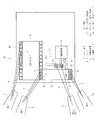
パワーMOSFETなどのパワー素子からソレノイドなどの負荷に流れる電流は、通常シャント抵抗を用いて検出される。図6は、従来のICチップの素子配置およびICチップとリードフレームの端子との接続態様を示している。また、図7は、当該ICチップに搭載された回路と外部に接続される回路の電気的構成を示している。 A current flowing from a power element such as a power MOSFET to a load such as a solenoid is usually detected using a shunt resistor. FIG. 6 shows an element arrangement of a conventional IC chip and a connection mode between the IC chip and a lead frame terminal. FIG. 7 shows an electrical configuration of a circuit mounted on the IC chip and a circuit connected to the outside.
ICチップ1には、パワーMOSFET2と制御回路3とが形成されており、MOSFET2のドレインに対応したパッド4とソースに対応したパッド5は、それぞれボンディングワイヤ6を介して端子7、8に接続されている。また、ICチップ1には、制御回路3の入力端子に対応してパッド9、10が形成されており、それぞれボンディングワイヤ6を介して端子11、12に接続されている。
A
このICをハイサイドスイッチとして用いる場合、図7に示すように端子7、8、12とグランドとの間にそれぞれ電源13、還流ダイオード14、ソレノイド15を接続するとともに、端子8と11とを接続し、端子11と12との間にシャント抵抗16を接続する。なお、シャント抵抗が内蔵されたICに係る先行技術文献については、先行技術調査により以下の特許文献1をはじめ複数発見されたが、本願発明に直接関連するものは発見されなかった。
上述した従来のICでは、シャント抵抗16をICチップ1とは別に設ける必要があり、ICのパッケージサイズの増大、コストの増加などの問題があった。
本発明は上記事情に鑑みてなされたもので、その目的は、電流検出用の抵抗が形成されたICチップを有する半導体装置を提供することにある。
In the above-described conventional IC, it is necessary to provide the
The present invention has been made in view of the above circumstances, and an object thereof is to provide a semiconductor device having an IC chip in which a resistor for current detection is formed.
請求項1に記載した手段によれば、同一の半導体基板にパワーMOSFETやパワートランジスタ等のパワー素子、当該パワー素子の主端子(ソース、ドレイン、エミッタ、コレクタ等)に接続される電流検出用の抵抗およびパワー素子を制御する制御回路を形成する。モノリシックICとすることにより、抵抗(シャント抵抗)をICチップとは別に設ける必要がない。
According to the means described in
この構成を採用するには、パワー素子および抵抗に流れる電流に偏りが生じない配置とする必要がある。そこで、本手段では、抵抗を、その電流通過方向に沿った辺がパワー素子のパッド列に直交する向きとなるようにパワー素子に隣接して形成している。この配置によれば、パワー素子から抵抗に流れ込む電流の実効的な電流経路を狭めることがなく、パワー素子および抵抗での電流集中(電流の偏り)を低減することができるので、発熱の増加を抑えられるとともに高い電流検出精度を確保できる。 In order to employ this configuration, it is necessary to arrange the current flowing in the power element and the resistor so that there is no bias. Therefore, in the present means, the resistor, sides along the current passing direction is formed adjacent to the power device so as to direct interlinking direction in the pad row of the power device. According to this arrangement, it is possible to reduce current concentration (current bias) in the power element and the resistor without narrowing the effective current path of the current flowing from the power element to the resistor. It can be suppressed and high current detection accuracy can be secured.
請求項2に記載した手段によれば、抵抗は、パワー素子の主端子のパッド列長に等しい幅を有し、当該抵抗の一端とパッド列とがその全幅において隣接するように形成されているので、パワー素子から抵抗に流れる電流は、パワー素子内部および抵抗内を均一に流れる。従って、一層発熱の増加を抑えられるとともに高い電流検出精度を確保できる。
According to the means described in
請求項3に記載した手段によれば、列状に形成されたパッドのうち等間隔に選択された複数のパッドと半導体チップの外部との間で配線がなされているので、半導体チップ外からパワー素子に流れ込む電流、半導体チップ外から抵抗に流れ込む電流はそれぞれパワー素子、抵抗に均等に流れ、パワー素子のスイッチング状態にかかわらずパワー素子および抵抗での電流の偏りを防止することができる。
According to the means described in
請求項4に記載した手段によれば、抵抗は、その幅の中心線とパワー素子のパッド列の中央位置とが一致するように形成されているので、同じパッド列長と抵抗幅の条件の下では、パワー素子から抵抗に流れ込む電流の実効的な電流経路が最も広くなり、且つ、抵抗の幅方向について電流が対称的に流れる。従って、抵抗での発熱の増加を抑えられるとともに高い電流検出精度を確保できる。
According to the means described in
請求項5に記載した手段によれば、請求項1または4に記載した構成に加え、パワー素子の列状に形成された主端子のパッドのうち抵抗と隣接する位置に形成されたパッドと半導体チップの外部との間で配線がなされているので、半導体チップ外から抵抗に流れ込む電流が抵抗に均等に流れ、パワー素子のスイッチング状態にかかわらず抵抗での電流の偏りを防止することができる。なお、本手段によれば、半導体チップ外からパワー素子に流れ込む電流もパワー素子に均等に流れ易くなる。
According to the means described in
請求項6に記載した手段によれば、抵抗から制御回路への引き出し用配線の少なくとも一方の途中に一対のパッドが設けられ、そのパッド同士は電気的に絶縁されている。この構成によれば、半導体基板単体の状態において制御回路から抵抗が切り離されているため、半導体チップの検査工程において制御回路の入力段の検査(例えばオペアンプのオフセット電圧等の検査)を容易に実施することができる。また、半導体装置の組立工程において第1のパッドと第2のパッドとを同一の端子に接続することにより、制御回路と抵抗とが接続される。
According to the means described in
(第1の実施形態)
以下、本発明の第1の実施形態について図1ないし図3を参照しながら説明する。
図1は、ICチップの素子配置およびICチップとリードフレームの端子との接続態様を示しており、図2は、当該ICチップに搭載された回路と外部に接続される回路の電気的構成を示している。これら図1、図2において、従来技術を示す図6、図7と同一部分には同一符号を付して示している。
(First embodiment)
Hereinafter, a first embodiment of the present invention will be described with reference to FIGS. 1 to 3.
FIG. 1 shows an element arrangement of an IC chip and a connection mode between the IC chip and a lead frame terminal, and FIG. 2 shows an electrical configuration of a circuit mounted on the IC chip and a circuit connected to the outside. Show. 1 and 2, the same parts as those in FIGS. 6 and 7 showing the prior art are denoted by the same reference numerals.
IC21(半導体装置に相当)は、ICチップ22(半導体チップに相当)をリードフレームに固定し、ICチップ22に形成された各パッドとリードフレームの端子7、8、11、12とをそれぞれボンディングワイヤ6で接続することにより組み立てられている。このIC21は、例えば車両のECU(Electronic Control Unit) に搭載され、ハイサイドスイッチとして動作して負荷であるソレノイド15に流れる電流を制御する。
The IC 21 (corresponding to a semiconductor device) fixes an IC chip 22 (corresponding to a semiconductor chip) to a lead frame, and bonds each pad formed on the
ICチップ22には、Nチャネル型パワーMOSFET2(パワー素子に相当)、当該MOSFET2を制御する制御回路3、アルミシャント抵抗23(電流検出用の抵抗に相当)および図示しないその他の制御回路が形成されている。MOSFET2には、ダイオード2aが形成されている。MOSFET2のドレイン(主端子)に対応した複数のパッド4とソース(主端子)に対応した複数のパッド5は、それぞれMOSFET2の素子形成領域の対向する辺部に沿って一列に形成されている。
The
シャント抵抗23は、その電流通過方向に沿った辺(図1では長辺)が上記MOSFET2の一列に並んだパッド5(以下、パッド列と称す)に直交する向きとなるようにMOSFET2に隣接して形成されている。シャント抵抗23の下には他の素子が形成されていないので、正確な抵抗値を持つシャント抵抗23を作ることができる。
The
また、シャント抵抗23を搭載することによりICチップ22の隅部(図1ではICチップ22の左下隅部)に無駄なスペースが生じないように、シャント抵抗23をICチップ22の左辺に沿って配置している。その結果、シャント抵抗23は、上記パッド列の中央ではなく左端側に寄って配置されることになる。シャント抵抗23の一端はMOSFET2のソースと電気的に接続され、他端にはパッド24が形成されている。パッド24は、ボンディングワイヤ6を介して端子12に接続されている。
In addition, by mounting the
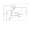
シャント抵抗23からは、その電流通過方向に所定間隔を隔てた電圧取り出し位置からビア25、26を介して配線27、28(引き出し用配線に相当)が引き出されている。配線27、28は、シャント抵抗23と制御回路3とを繋ぐもので、このうち配線28は、直接制御回路3に至るように形成されている。一方、配線27は、シャント抵抗23から第1のパッド29に至る第1の配線27aと、第1のパッド29に近接して形成された第2のパッド30から制御回路3に至る第2の配線27bとから構成されている。パッド29、30は、それぞれボンディングワイヤ6を介して共通の端子11に接続されている。
制御回路3の入力段は、オペアンプ31を用いた差動増幅回路であって、配線27(27b)は抵抗32を介してオペアンプ31の非反転入力端子に接続され、配線28は抵抗33を介してオペアンプ31の反転入力端子に接続されている。オペアンプ31の反転入力端子と出力端子との間には抵抗34が接続されている。
The input stage of the
MOSFET2のソースのパッド5のうちシャント抵抗23と相対する位置(パッド列の左端側)に形成された3つのパッド5は、それぞれボンディングワイヤ6を介して端子8に接続されている。一方、MOSFET2のドレインのパッド4のうち、ほぼ中央から右端にかけて等間隔に選択された3つのパッド4は、それぞれボンディングワイヤ6を介して端子7に接続されている。換言すれば、MOSFET2の素子形成領域のほぼ対角付近に位置するパッド4とパッド5に対し、ボンディングワイヤ6が打たれている。
Of the
IC21を用いる場合、端子7、8、12とグランドとの間にそれぞれ電源13、還流ダイオード14、ソレノイド15が外付けされる。従来構成とは異なり、外付けのシャント抵抗は不要である。また、端子11は、IC21の組み立て工程においてパッド29と30とを接続するために用いられ、IC21を実際に使用する際には通常用いられない。ただし、端子11の電位は端子8の電位と等しいため、端子11を電圧検出端子として用いることは可能である。
When the
図3は、シャント抵抗23と配線27、28との接続部を示すICチップ22の縦断面図である。保護膜は省略している。例えば配線層が3層のアルミ配線からなる場合、(a)は、配線27、28が第2層目のアルミ配線(第2アルミ配線)で形成され、シャント抵抗23が第3層目のアルミ配線(第3アルミ配線)により形成された場合を示している。(b)は、シャント抵抗23が第2層目のアルミ配線(第2アルミ配線)により形成され、配線27、28が第3層目のアルミ配線(第3アルミ配線)で形成された場合を示している。
FIG. 3 is a longitudinal sectional view of the
図3(a)に示す場合、シリコン基板35(半導体基板に相当)の上に層間膜36が形成され、その上にアルミ配線27、28がパターニングにより形成され、さらに層間膜37が形成されている。その上にはスパッタによりアルミシャント抵抗23が形成されている。アルミ配線27、28とアルミシャント抵抗23とは、それぞれビア25、26により接続されている。一方、図3(b)に示す場合、シリコン基板35の上に層間膜36が形成され、その上にはスパッタによりアルミシャント抵抗23が形成されている。その上には、層間膜37が形成され、さらにパターニングによりアルミ配線27、28が形成されている。アルミシャント抵抗23とアルミ配線27、28とは、それぞれビア25、26により接続されている。
In the case shown in FIG. 3A, an
次に、IC21の作用および効果について説明する。
図2において、IC21をハイサイドスイッチとして用いる場合、制御回路3は、図示しないチャージポンプ回路の出力電圧を用いて、MOSFET2のゲートに駆動電圧を与える。MOSFET2がオンすると、電源13から端子7、MOSFET2、シャント抵抗23、端子12、ソレノイド15の経路で主回路電流が流れ、MOSFET2がオフすると、還流ダイオード14、端子8、シャント抵抗23、端子12、ソレノイド15の経路で還流電流が流れる。制御回路3は、シャント抵抗23から配線27、28によって取り出される電圧に基づいて、ソレノイド15に流れる電流を制御する。
Next, the operation and effect of the
In FIG. 2, when the
さらに電流の流れを詳しく見ると、MOSFET2がオンしている期間、MOSFET2には、パッド4から流れ込んだ電流が素子全体に分散して対角方向に流れ、シャント抵抗23へと流れ込む。つまり、シャント抵抗23と相対する位置にあるパッド5に対しMOSFET2の素子形成領域をほぼ対角に隔てた位置にあるパッド4にボンディングすることにより、素子内部での実効的な電流経路が広くなり電流の均一化が図られる。
Further, when the current flow is examined in detail, during the period when the
そして、シャント抵抗23は、その電流通過方向に沿った辺がMOSFET2のパッド列に直角となるように形成されているので、MOSFET2からシャント抵抗23に流れ込む電流の実効的な電流経路が制限されることがなく、MOSFET2とシャント抵抗23との接続部付近における電流集中(電流の偏り)を防止することができ、電流がシャント抵抗23の幅方向に均一に広がって流れる。これにより、発熱の増加が抑えられ、高い電流検出精度を確保できる。
Since the
また、シャント抵抗23と相対する位置に形成されたパッド5と端子8とが接続されているので、MOSFET2がオフしている期間、シャント抵抗23にはパッド5から流れ込んだ還流電流が幅方向に均等に分散して流れる。従って、還流期間においても、シャント抵抗23での発熱の増加を抑えられ且つ高い電流検出精度を確保できる。
In addition, since the
さらに、ICチップ22においてシャント抵抗23から制御回路3への引き出し用の配線27の途中に一対のパッド29、30が設けられており、当該パッド29と30は、組立工程において端子11を介して接続されるようになっている。ICチップ22単体の検査工程においてオペアンプ31の検査を行う場合、オペアンプ31の入力端子からシャント抵抗23が切り離された状態となるため、検査を容易に実施することができる。また、配線27、28はセンシング用の配線であるため電流は殆ど流れない。このため、パッド29と30とをボンディングワイヤ6を用いて接続しても検出精度の低下は生じない。
Further, a pair of
(第2の実施形態)
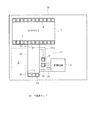
図4は、本発明の第2の実施形態におけるICチップの素子配置を示している。
ICチップ38(半導体チップに相当)は、第1の実施形態で説明したICチップ22に対しシャント抵抗23の配置が異なっている。すなわち、シャント抵抗23は、その幅の中心線とMOSFET2のパッド列の中央位置とが一致するように形成されている。
(Second Embodiment)
FIG. 4 shows an element arrangement of the IC chip in the second embodiment of the present invention.
The IC chip 38 (corresponding to a semiconductor chip) is different from the
このような配置とすることにより、MOSFET2がオンしている期間、MOSFET2内部での実効的な電流経路が広くなり、パッド4から流れ込んだ電流が素子全体に分散して均一に流れ易くなる。また、MOSFET2とシャント抵抗23との接続部付近における電流集中(電流の偏り)をより一層低減することができる。これにより、発熱の増加を抑えられるとともに高い電流検出精度を確保できる。
With this arrangement, an effective current path inside the
なお、ICチップ38のパッド24、29、30とリードフレームの端子との間で配線を行うと、配線の相互干渉により図4に示す左下隅部Aに別のパッド(ひいては別の回路)を設けることが難しくなる。従って、左下隅部Aにも回路を形成して有効に利用するためには、パッドと端子との間の配線方向が基板に対し垂直方向となるCSP(Chip Scale Package)を用いることが好ましい。
When wiring is performed between the
(第3の実施形態)
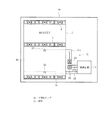
図5は、本発明の第2の実施形態におけるICチップの素子配置を示している。
ICチップ39(半導体チップに相当)において、シャント抵抗40は、MOSFET2のパッド列長に等しい幅を有し、当該シャント抵抗40とパッド列とがその全幅において相対するように形成されている。このような配置によれば、MOSFET2からシャント抵抗40に流れ込む電流およびパッド5からシャント抵抗40に流れ込む還流電流は、MOSFET2の内部およびシャント抵抗40の内部を均一に流れる。従って、より一層発熱の増加を抑えられるとともに高い電流検出精度を確保できる。
(Third embodiment)
FIG. 5 shows an element arrangement of the IC chip in the second embodiment of the present invention.
In the IC chip 39 (corresponding to a semiconductor chip), the
(その他の実施形態)
なお、本発明は上記し且つ図面に示す各実施形態に限定されるものではなく、例えば以下のように変形または拡張が可能である。
シャント抵抗23、40は、その電流通過方向に沿った辺がMOSFET2のパッド列に直交する向きとなることが最も好ましい配置であるが、正確に直交する向きでなくても上述した効果を得ることができる。
(Other embodiments)
The present invention is not limited to the embodiments described above and shown in the drawings, and can be modified or expanded as follows, for example.
The shunt resistors 23 and 40 are most preferably arranged such that the sides along the current passing direction are perpendicular to the pad row of the
配線28についても、配線27と同様に一対のパッドを介した絶縁部を設けてもよい。また、パッド29と30は、必ずしも近接して設けなくてもよい。
シャント抵抗23、40と配線27、28とを接続するビア25、26は、それぞれ複数設けてもよい。
シャント抵抗23、40は、アルミニウムに限らず他の金属材料や半導体材料を用いて構成してもよい。
Similarly to the
A plurality of
The shunt resistors 23 and 40 are not limited to aluminum and may be configured using other metal materials or semiconductor materials.
2はパワーMOSFET(パワー素子)、3は制御回路、4、5はパッド、21はIC(半導体装置)、22、38、39はICチップ(半導体チップ)、23、40は抵抗、27、28は配線(引き出し用配線)、27a、27bは配線(第1、第2の配線)、29、30はパッド(第1、第2のパッド)、35はシリコン基板(半導体基板)である。 2 is a power MOSFET (power element), 3 is a control circuit, 4 and 5 are pads, 21 is an IC (semiconductor device), 22, 38 and 39 are IC chips (semiconductor chips), 23 and 40 are resistors, and 27 and 28 Are wiring (leading wiring), 27a and 27b are wiring (first and second wiring), 29 and 30 are pads (first and second pads), and 35 is a silicon substrate (semiconductor substrate).
Claims (6)
前記パワー素子の主端子のパッドは、当該パワー素子の素子形成領域の辺部に沿って列状に形成されており、
前記抵抗は、その電流通過方向に沿った辺が前記パワー素子のパッド列に直交する向きとなるように前記パワー素子に隣接して形成されていることを特徴とする半導体装置。 A semiconductor chip on which a power element, a resistor for current detection connected to a main terminal of the power element, and a control circuit for controlling the power element are formed on the same semiconductor substrate,
The pad of the main terminal of the power element is formed in a row along the side of the element formation region of the power element,
The resistor is a semiconductor device which is characterized in that edges along its current passing direction is formed adjacent to the power device so as to direct interlinking direction in the pad row of the power device.
その引き出し用配線の少なくとも一方は、前記抵抗から第1のパッドに至る第1の配線と、前記第1のパッドと絶縁された第2のパッドから前記制御回路に至る第2の配線とから構成されていることを特徴とする請求項1ないし5の何れかに記載の半導体装置。 In the resistor, a pair of lead-out wirings from the position spaced in the current passage direction to the control circuit is formed,
At least one of the lead-out wirings includes a first wiring from the resistor to the first pad, and a second wiring from the second pad insulated from the first pad to the control circuit. 6. The semiconductor device according to claim 1, wherein the semiconductor device is formed.
Priority Applications (1)
| Application Number | Priority Date | Filing Date | Title |
|---|---|---|---|
| JP2004351183A JP4144591B2 (en) | 2004-12-03 | 2004-12-03 | Semiconductor device |
Applications Claiming Priority (1)
| Application Number | Priority Date | Filing Date | Title |
|---|---|---|---|
| JP2004351183A JP4144591B2 (en) | 2004-12-03 | 2004-12-03 | Semiconductor device |
Publications (2)
| Publication Number | Publication Date |
|---|---|
| JP2006165100A JP2006165100A (en) | 2006-06-22 |
| JP4144591B2 true JP4144591B2 (en) | 2008-09-03 |
Family
ID=36666789
Family Applications (1)
| Application Number | Title | Priority Date | Filing Date |
|---|---|---|---|
| JP2004351183A Expired - Fee Related JP4144591B2 (en) | 2004-12-03 | 2004-12-03 | Semiconductor device |
Country Status (1)
| Country | Link |
|---|---|
| JP (1) | JP4144591B2 (en) |
Families Citing this family (9)
| Publication number | Priority date | Publication date | Assignee | Title |
|---|---|---|---|---|
| JP5194585B2 (en) * | 2007-06-29 | 2013-05-08 | 富士電機株式会社 | Semiconductor device testing method |
| JP4513920B2 (en) * | 2008-06-19 | 2010-07-28 | 株式会社デンソー | Constant current control circuit |
| JP2011069809A (en) * | 2009-08-31 | 2011-04-07 | Hitachi Automotive Systems Ltd | Control system and semiconductor device used therein |
| JP5280332B2 (en) | 2009-10-30 | 2013-09-04 | 日立オートモティブシステムズ株式会社 | Semiconductor device for current control and control device using the same |
| JP5406145B2 (en) | 2010-08-31 | 2014-02-05 | 日立オートモティブシステムズ株式会社 | Semiconductor device for current control and control device using the same |
| JP5395127B2 (en) | 2011-07-14 | 2014-01-22 | 日立オートモティブシステムズ株式会社 | Semiconductor device for current control and control device using the same |
| JP6541223B2 (en) * | 2015-01-16 | 2019-07-10 | 新日本無線株式会社 | Semiconductor device |
| JP6957892B2 (en) * | 2016-08-02 | 2021-11-02 | 富士電機株式会社 | Semiconductor devices and their characteristic evaluation methods |
| DE102018207308B4 (en) * | 2018-05-09 | 2020-07-02 | Infineon Technologies Ag | SEMICONDUCTOR COMPONENT WITH INTEGRATED SHUNT RESISTANCE AND METHOD FOR THE PRODUCTION THEREOF |
-
2004
- 2004-12-03 JP JP2004351183A patent/JP4144591B2/en not_active Expired - Fee Related
Also Published As
| Publication number | Publication date |
|---|---|
| JP2006165100A (en) | 2006-06-22 |
Similar Documents
| Publication | Publication Date | Title |
|---|---|---|
| US20230317713A1 (en) | Semiconductor Device | |
| JP4807768B2 (en) | Power transistor device and power control system using the same | |
| JP5526849B2 (en) | Semiconductor device | |
| CN106558583A (en) | Semiconductor device | |
| US6529062B2 (en) | Power module | |
| CN101276811A (en) | Semiconductor device with a plurality of transistors | |
| JP4144591B2 (en) | Semiconductor device | |
| JP2008533734A (en) | MOSFET with temperature sensing function | |
| TW201532162A (en) | Semiconductor integrated circuit device | |
| JPH09283632A (en) | Semiconductor integrated circuit device | |
| KR100194312B1 (en) | Semiconductor device with electrostatic breakdown protection circuit | |
| JP7090044B2 (en) | Semiconductor equipment | |
| CN116298456A (en) | current measurement circuit | |
| JPS63141357A (en) | Power mosfet | |
| JP6890480B2 (en) | Semiconductor device | |
| US7122882B2 (en) | Low cost power MOSFET with current monitoring | |
| JPH11121683A (en) | Semiconductor integrated circuit | |
| US7714363B2 (en) | Semiconductor integrated circuit for driving the address of a display device | |
| JP3383451B2 (en) | Semiconductor device | |
| JP2570990B2 (en) | Semiconductor integrated circuit | |
| JP2676801B2 (en) | Semiconductor integrated circuit device having output buffer circuit | |
| CN104247027A (en) | power transistor module | |
| JP2001156178A (en) | Semiconductor device and automatic layout method for the same | |
| US7719254B2 (en) | Method for setting a reference potential of a current sensor and arrangement for determining the reference potential of a power semiconductor device | |
| JP7707658B2 (en) | Integrated circuit device |
Legal Events
| Date | Code | Title | Description |
|---|---|---|---|
| A977 | Report on retrieval |
Free format text: JAPANESE INTERMEDIATE CODE: A971007 Effective date: 20071220 |
|
| A131 | Notification of reasons for refusal |
Free format text: JAPANESE INTERMEDIATE CODE: A131 Effective date: 20080408 |
|
| A521 | Request for written amendment filed |
Free format text: JAPANESE INTERMEDIATE CODE: A523 Effective date: 20080425 |
|
| TRDD | Decision of grant or rejection written | ||
| A01 | Written decision to grant a patent or to grant a registration (utility model) |
Free format text: JAPANESE INTERMEDIATE CODE: A01 Effective date: 20080527 |
|
| A01 | Written decision to grant a patent or to grant a registration (utility model) |
Free format text: JAPANESE INTERMEDIATE CODE: A01 |
|
| A61 | First payment of annual fees (during grant procedure) |
Free format text: JAPANESE INTERMEDIATE CODE: A61 Effective date: 20080609 |
|
| R150 | Certificate of patent or registration of utility model |
Free format text: JAPANESE INTERMEDIATE CODE: R150 |
|
| FPAY | Renewal fee payment (event date is renewal date of database) |
Free format text: PAYMENT UNTIL: 20110627 Year of fee payment: 3 |
|
| FPAY | Renewal fee payment (event date is renewal date of database) |
Free format text: PAYMENT UNTIL: 20110627 Year of fee payment: 3 |
|
| FPAY | Renewal fee payment (event date is renewal date of database) |
Free format text: PAYMENT UNTIL: 20120627 Year of fee payment: 4 |
|
| FPAY | Renewal fee payment (event date is renewal date of database) |
Free format text: PAYMENT UNTIL: 20120627 Year of fee payment: 4 |
|
| FPAY | Renewal fee payment (event date is renewal date of database) |
Free format text: PAYMENT UNTIL: 20130627 Year of fee payment: 5 |
|
| FPAY | Renewal fee payment (event date is renewal date of database) |
Free format text: PAYMENT UNTIL: 20140627 Year of fee payment: 6 |
|
| R250 | Receipt of annual fees |
Free format text: JAPANESE INTERMEDIATE CODE: R250 |
|
| LAPS | Cancellation because of no payment of annual fees |