JP4112729B2 - 半導体装置 - Google Patents
半導体装置 Download PDFInfo
- Publication number
- JP4112729B2 JP4112729B2 JP03695399A JP3695399A JP4112729B2 JP 4112729 B2 JP4112729 B2 JP 4112729B2 JP 03695399 A JP03695399 A JP 03695399A JP 3695399 A JP3695399 A JP 3695399A JP 4112729 B2 JP4112729 B2 JP 4112729B2
- Authority
- JP
- Japan
- Prior art keywords
- circuit
- signal
- memory cell
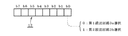
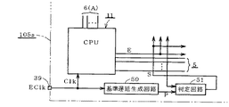
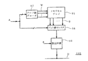
- read
- cpu
- Prior art date
- Legal status (The legal status is an assumption and is not a legal conclusion. Google has not performed a legal analysis and makes no representation as to the accuracy of the status listed.)
- Expired - Fee Related
Links
- 239000004065 semiconductor Substances 0.000 title claims description 40
- 238000010586 diagram Methods 0.000 description 43
- 230000008859 change Effects 0.000 description 6
- 238000003491 array Methods 0.000 description 5
- 230000004048 modification Effects 0.000 description 4
- 238000012986 modification Methods 0.000 description 4
- 230000000630 rising effect Effects 0.000 description 4
- 230000004044 response Effects 0.000 description 3
- 230000000694 effects Effects 0.000 description 2
- 230000003321 amplification Effects 0.000 description 1
- 230000008901 benefit Effects 0.000 description 1
- 239000003990 capacitor Substances 0.000 description 1
- 230000003111 delayed effect Effects 0.000 description 1
- 230000006866 deterioration Effects 0.000 description 1
- 230000006870 function Effects 0.000 description 1
- 230000006872 improvement Effects 0.000 description 1
- 230000010354 integration Effects 0.000 description 1
- 239000011159 matrix material Substances 0.000 description 1
- 238000003199 nucleic acid amplification method Methods 0.000 description 1
- 230000002093 peripheral effect Effects 0.000 description 1
Images


Classifications
-
- G—PHYSICS
- G11—INFORMATION STORAGE
- G11C—STATIC STORES
- G11C7/00—Arrangements for writing information into, or reading information out from, a digital store
- G11C7/06—Sense amplifiers; Associated circuits, e.g. timing or triggering circuits
- G11C7/062—Differential amplifiers of non-latching type, e.g. comparators, long-tailed pairs
-
- G—PHYSICS
- G11—INFORMATION STORAGE
- G11C—STATIC STORES
- G11C7/00—Arrangements for writing information into, or reading information out from, a digital store
- G11C7/06—Sense amplifiers; Associated circuits, e.g. timing or triggering circuits
Landscapes
- Dram (AREA)
- Static Random-Access Memory (AREA)
- Read Only Memory (AREA)
Priority Applications (2)
| Application Number | Priority Date | Filing Date | Title |
|---|---|---|---|
| JP03695399A JP4112729B2 (ja) | 1999-02-16 | 1999-02-16 | 半導体装置 |
| US09/411,836 US6219300B1 (en) | 1999-02-16 | 1999-10-04 | Semiconductor device |
Applications Claiming Priority (1)
| Application Number | Priority Date | Filing Date | Title |
|---|---|---|---|
| JP03695399A JP4112729B2 (ja) | 1999-02-16 | 1999-02-16 | 半導体装置 |
Publications (3)
| Publication Number | Publication Date |
|---|---|
| JP2000235796A JP2000235796A (ja) | 2000-08-29 |
| JP2000235796A5 JP2000235796A5 (enExample) | 2005-10-27 |
| JP4112729B2 true JP4112729B2 (ja) | 2008-07-02 |
Family
ID=12484121
Family Applications (1)
| Application Number | Title | Priority Date | Filing Date |
|---|---|---|---|
| JP03695399A Expired - Fee Related JP4112729B2 (ja) | 1999-02-16 | 1999-02-16 | 半導体装置 |
Country Status (2)
| Country | Link |
|---|---|
| US (1) | US6219300B1 (enExample) |
| JP (1) | JP4112729B2 (enExample) |
Cited By (1)
| Publication number | Priority date | Publication date | Assignee | Title |
|---|---|---|---|---|
| JPH0751920A (ja) * | 1993-08-19 | 1995-02-28 | Techno Sakato:Kk | 軸装置及び該軸装置を用いたカッター |
Families Citing this family (27)
| Publication number | Priority date | Publication date | Assignee | Title |
|---|---|---|---|---|
| JP2001222899A (ja) * | 1999-11-30 | 2001-08-17 | Seiko Epson Corp | 半導体集積回路 |
| US20030112665A1 (en) * | 2001-12-17 | 2003-06-19 | Nec Electronics Corporation | Semiconductor memory device, data processor, and method of determining frequency |
| US7106636B2 (en) * | 2004-06-22 | 2006-09-12 | Intel Corporation | Partitionable memory device, system, and method |
| KR100672147B1 (ko) * | 2005-03-15 | 2007-01-19 | 주식회사 하이닉스반도체 | 불휘발성 메모리 장치의 체크 보드 프로그램 시에 프로그램페일을 방지하기 위한 페이지 버퍼 |
| KR100756798B1 (ko) | 2006-04-24 | 2007-09-07 | 주식회사 하이닉스반도체 | Rfid 장치 |
| US7536570B2 (en) * | 2006-10-02 | 2009-05-19 | Silicon Laboratories Inc. | Microcontroller unit (MCU) with suspend mode |
| US7886084B2 (en) | 2007-06-26 | 2011-02-08 | International Business Machines Corporation | Optimized collectives using a DMA on a parallel computer |
| US8108738B2 (en) | 2007-06-26 | 2012-01-31 | International Business Machines Corporation | Data eye monitor method and apparatus |
| US7984448B2 (en) * | 2007-06-26 | 2011-07-19 | International Business Machines Corporation | Mechanism to support generic collective communication across a variety of programming models |
| US8230433B2 (en) | 2007-06-26 | 2012-07-24 | International Business Machines Corporation | Shared performance monitor in a multiprocessor system |
| US7873843B2 (en) * | 2007-06-26 | 2011-01-18 | International Business Machines Corporation | Static power reduction for midpoint-terminated busses |
| US8458282B2 (en) | 2007-06-26 | 2013-06-04 | International Business Machines Corporation | Extended write combining using a write continuation hint flag |
| US7877551B2 (en) * | 2007-06-26 | 2011-01-25 | International Business Machines Corporation | Programmable partitioning for high-performance coherence domains in a multiprocessor system |
| US8468416B2 (en) | 2007-06-26 | 2013-06-18 | International Business Machines Corporation | Combined group ECC protection and subgroup parity protection |
| US7827391B2 (en) | 2007-06-26 | 2010-11-02 | International Business Machines Corporation | Method and apparatus for single-stepping coherence events in a multiprocessor system under software control |
| US8103832B2 (en) * | 2007-06-26 | 2012-01-24 | International Business Machines Corporation | Method and apparatus of prefetching streams of varying prefetch depth |
| US7802025B2 (en) | 2007-06-26 | 2010-09-21 | International Business Machines Corporation | DMA engine for repeating communication patterns |
| US8032892B2 (en) * | 2007-06-26 | 2011-10-04 | International Business Machines Corporation | Message passing with a limited number of DMA byte counters |
| US8010875B2 (en) | 2007-06-26 | 2011-08-30 | International Business Machines Corporation | Error correcting code with chip kill capability and power saving enhancement |
| US8140925B2 (en) | 2007-06-26 | 2012-03-20 | International Business Machines Corporation | Method and apparatus to debug an integrated circuit chip via synchronous clock stop and scan |
| US7793038B2 (en) | 2007-06-26 | 2010-09-07 | International Business Machines Corporation | System and method for programmable bank selection for banked memory subsystems |
| US8756350B2 (en) | 2007-06-26 | 2014-06-17 | International Business Machines Corporation | Method and apparatus for efficiently tracking queue entries relative to a timestamp |
| US8509255B2 (en) | 2007-06-26 | 2013-08-13 | International Business Machines Corporation | Hardware packet pacing using a DMA in a parallel computer |
| EP2539897B1 (en) * | 2010-02-23 | 2020-03-18 | Rambus Inc. | Methods and circuits for dynamically scaling dram power and performance |
| JP5328957B2 (ja) * | 2012-04-17 | 2013-10-30 | ルネサスエレクトロニクス株式会社 | 半導体記憶装置 |
| TWI610179B (zh) * | 2016-12-07 | 2018-01-01 | 慧榮科技股份有限公司 | 主機裝置與資料傳輸速率控制方法 |
| JP2020004119A (ja) * | 2018-06-28 | 2020-01-09 | ルネサスエレクトロニクス株式会社 | 半導体装置およびそれを用いた制御システム |
Family Cites Families (5)
| Publication number | Priority date | Publication date | Assignee | Title |
|---|---|---|---|---|
| JP2743653B2 (ja) | 1991-09-20 | 1998-04-22 | 富士通株式会社 | 半導体記憶装置 |
| JPH06275081A (ja) | 1993-03-18 | 1994-09-30 | Fujitsu Ltd | 半導体記憶装置 |
| US5497355A (en) * | 1994-06-03 | 1996-03-05 | Intel Corporation | Synchronous address latching for memory arrays |
| JPH10275140A (ja) * | 1997-03-31 | 1998-10-13 | Nec Ic Microcomput Syst Ltd | マイクロコンピュータ |
| JP3090104B2 (ja) * | 1997-10-27 | 2000-09-18 | 日本電気株式会社 | 半導体メモリ装置 |
-
1999
- 1999-02-16 JP JP03695399A patent/JP4112729B2/ja not_active Expired - Fee Related
- 1999-10-04 US US09/411,836 patent/US6219300B1/en not_active Expired - Lifetime
Cited By (1)
| Publication number | Priority date | Publication date | Assignee | Title |
|---|---|---|---|---|
| JPH0751920A (ja) * | 1993-08-19 | 1995-02-28 | Techno Sakato:Kk | 軸装置及び該軸装置を用いたカッター |
Also Published As
| Publication number | Publication date |
|---|---|
| JP2000235796A (ja) | 2000-08-29 |
| US6219300B1 (en) | 2001-04-17 |
Similar Documents
| Publication | Publication Date | Title |
|---|---|---|
| JP4112729B2 (ja) | 半導体装置 | |
| US7227777B2 (en) | Mode selection in a flash memory device | |
| JP5461526B2 (ja) | 電気的メモリ動作におけるダイナミック電力セービングのためのシステム及び方法 | |
| TWI404063B (zh) | 記憶體系統及用於記憶體之控制方法 | |
| JP3754593B2 (ja) | データビットを記憶するメモリーセルを有する集積回路および集積回路において書き込みデータビットをメモリーセルに書き込む方法 | |
| US4961172A (en) | Decoder for a memory address bus | |
| JPH10242842A (ja) | マイクロコントローラアクセス可能マクロセル | |
| US10529407B2 (en) | Memory device including a plurality of power rails and method of operating the same | |
| JP2599841B2 (ja) | データ処理装置 | |
| US5623221A (en) | Low noise MOSFET employing selective drive signals | |
| US6937515B2 (en) | Semiconductor memory device | |
| JPS6249676B2 (enExample) | ||
| JP5038657B2 (ja) | 半導体集積回路装置 | |
| JPS58139392A (ja) | 半導体メモリ | |
| CN113948134A (zh) | 存储装置及其输入输出缓冲控制方法 | |
| US6404688B2 (en) | Semiconductor memory device having a self-refresh operation | |
| US7978547B2 (en) | Data I/O control signal generating circuit in a semiconductor memory apparatus | |
| JPH09180443A (ja) | 半導体メモリ回路 | |
| US6157211A (en) | FPGA using RAM control signal lines as routing or logic resources after configuration | |
| US6246633B1 (en) | Semiconductor memory device permitting stabilized operation and high-speed access | |
| JP2937203B2 (ja) | 半導体メモリ装置 | |
| JP2616184B2 (ja) | 半動体メモリ装置 | |
| JP2002230979A (ja) | 半導体メモリおよびその制御回路 | |
| JPH1116356A (ja) | 半導体メモリのプリチャージ方式 | |
| JPH11110990A (ja) | 半導体記憶装置 |
Legal Events
| Date | Code | Title | Description |
|---|---|---|---|
| A521 | Written amendment |
Free format text: JAPANESE INTERMEDIATE CODE: A523 Effective date: 20050707 |
|
| A621 | Written request for application examination |
Free format text: JAPANESE INTERMEDIATE CODE: A621 Effective date: 20050707 |
|
| A131 | Notification of reasons for refusal |
Free format text: JAPANESE INTERMEDIATE CODE: A131 Effective date: 20080108 |
|
| A521 | Written amendment |
Free format text: JAPANESE INTERMEDIATE CODE: A523 Effective date: 20080227 |
|
| RD04 | Notification of resignation of power of attorney |
Free format text: JAPANESE INTERMEDIATE CODE: A7424 Effective date: 20080227 |
|
| TRDD | Decision of grant or rejection written | ||
| A01 | Written decision to grant a patent or to grant a registration (utility model) |
Free format text: JAPANESE INTERMEDIATE CODE: A01 Effective date: 20080408 |
|
| A61 | First payment of annual fees (during grant procedure) |
Free format text: JAPANESE INTERMEDIATE CODE: A61 Effective date: 20080410 |
|
| R150 | Certificate of patent or registration of utility model |
Free format text: JAPANESE INTERMEDIATE CODE: R150 |
|
| FPAY | Renewal fee payment (event date is renewal date of database) |
Free format text: PAYMENT UNTIL: 20110418 Year of fee payment: 3 |
|
| FPAY | Renewal fee payment (event date is renewal date of database) |
Free format text: PAYMENT UNTIL: 20110418 Year of fee payment: 3 |
|
| S111 | Request for change of ownership or part of ownership |
Free format text: JAPANESE INTERMEDIATE CODE: R313111 |
|
| FPAY | Renewal fee payment (event date is renewal date of database) |
Free format text: PAYMENT UNTIL: 20110418 Year of fee payment: 3 |
|
| R350 | Written notification of registration of transfer |
Free format text: JAPANESE INTERMEDIATE CODE: R350 |
|
| FPAY | Renewal fee payment (event date is renewal date of database) |
Free format text: PAYMENT UNTIL: 20120418 Year of fee payment: 4 |
|
| FPAY | Renewal fee payment (event date is renewal date of database) |
Free format text: PAYMENT UNTIL: 20120418 Year of fee payment: 4 |
|
| FPAY | Renewal fee payment (event date is renewal date of database) |
Free format text: PAYMENT UNTIL: 20130418 Year of fee payment: 5 |
|
| FPAY | Renewal fee payment (event date is renewal date of database) |
Free format text: PAYMENT UNTIL: 20140418 Year of fee payment: 6 |
|
| S531 | Written request for registration of change of domicile |
Free format text: JAPANESE INTERMEDIATE CODE: R313531 |
|
| R350 | Written notification of registration of transfer |
Free format text: JAPANESE INTERMEDIATE CODE: R350 |
|
| LAPS | Cancellation because of no payment of annual fees |