JP4030758B2 - Method for manufacturing semiconductor device - Google Patents
Method for manufacturing semiconductor device Download PDFInfo
- Publication number
- JP4030758B2 JP4030758B2 JP2001401281A JP2001401281A JP4030758B2 JP 4030758 B2 JP4030758 B2 JP 4030758B2 JP 2001401281 A JP2001401281 A JP 2001401281A JP 2001401281 A JP2001401281 A JP 2001401281A JP 4030758 B2 JP4030758 B2 JP 4030758B2
- Authority
- JP
- Japan
- Prior art keywords
- island
- shaped semiconductor
- semiconductor films
- laser
- film
- Prior art date
- Legal status (The legal status is an assumption and is not a legal conclusion. Google has not performed a legal analysis and makes no representation as to the accuracy of the status listed.)
- Expired - Fee Related
Links
- 239000004065 semiconductor Substances 0.000 title claims description 484
- 238000000034 method Methods 0.000 title claims description 89
- 238000004519 manufacturing process Methods 0.000 title claims description 55
- 239000000758 substrate Substances 0.000 claims description 140
- 238000000059 patterning Methods 0.000 claims description 35
- 230000015572 biosynthetic process Effects 0.000 claims description 25
- 238000010438 heat treatment Methods 0.000 claims description 15
- 230000001678 irradiating effect Effects 0.000 claims description 14
- 239000007789 gas Substances 0.000 claims description 11
- 229910052751 metal Inorganic materials 0.000 claims description 10
- 239000002184 metal Substances 0.000 claims description 10
- 239000011521 glass Substances 0.000 claims description 8
- 239000010949 copper Substances 0.000 claims description 7
- 229910052802 copper Inorganic materials 0.000 claims description 5
- 239000010931 gold Substances 0.000 claims description 4
- 239000010979 ruby Substances 0.000 claims description 4
- 229910001750 ruby Inorganic materials 0.000 claims description 4
- RYGMFSIKBFXOCR-UHFFFAOYSA-N Copper Chemical compound [Cu] RYGMFSIKBFXOCR-UHFFFAOYSA-N 0.000 claims description 3
- PCHJSUWPFVWCPO-UHFFFAOYSA-N gold Chemical compound [Au] PCHJSUWPFVWCPO-UHFFFAOYSA-N 0.000 claims description 3
- 229910052737 gold Inorganic materials 0.000 claims description 3
- UIZLQMLDSWKZGC-UHFFFAOYSA-N cadmium helium Chemical compound [He].[Cd] UIZLQMLDSWKZGC-UHFFFAOYSA-N 0.000 claims description 2
- 239000010410 layer Substances 0.000 description 280
- 239000010408 film Substances 0.000 description 253
- 239000012535 impurity Substances 0.000 description 55
- 239000011229 interlayer Substances 0.000 description 33
- 239000000463 material Substances 0.000 description 33
- 230000008569 process Effects 0.000 description 32
- 239000002585 base Substances 0.000 description 28
- 238000005530 etching Methods 0.000 description 23
- 239000013078 crystal Substances 0.000 description 22
- 239000003550 marker Substances 0.000 description 21
- 229910052710 silicon Inorganic materials 0.000 description 21
- 230000003287 optical effect Effects 0.000 description 20
- XUIMIQQOPSSXEZ-UHFFFAOYSA-N Silicon Chemical compound [Si] XUIMIQQOPSSXEZ-UHFFFAOYSA-N 0.000 description 19
- 238000002425 crystallisation Methods 0.000 description 19
- 239000010703 silicon Substances 0.000 description 19
- 230000008025 crystallization Effects 0.000 description 16
- 238000012545 processing Methods 0.000 description 15
- 238000004544 sputter deposition Methods 0.000 description 11
- 229910052581 Si3N4 Inorganic materials 0.000 description 10
- 238000010586 diagram Methods 0.000 description 10
- 239000011159 matrix material Substances 0.000 description 10
- VYPSYNLAJGMNEJ-UHFFFAOYSA-N silicon dioxide Inorganic materials O=[Si]=O VYPSYNLAJGMNEJ-UHFFFAOYSA-N 0.000 description 10
- HQVNEWCFYHHQES-UHFFFAOYSA-N silicon nitride Chemical compound N12[Si]34N5[Si]62N3[Si]51N64 HQVNEWCFYHHQES-UHFFFAOYSA-N 0.000 description 10
- 239000010936 titanium Substances 0.000 description 10
- OAICVXFJPJFONN-UHFFFAOYSA-N Phosphorus Chemical compound [P] OAICVXFJPJFONN-UHFFFAOYSA-N 0.000 description 9
- PXHVJJICTQNCMI-UHFFFAOYSA-N nickel Substances [Ni] PXHVJJICTQNCMI-UHFFFAOYSA-N 0.000 description 9
- 229910052698 phosphorus Inorganic materials 0.000 description 9
- 239000011574 phosphorus Substances 0.000 description 9
- 239000011347 resin Substances 0.000 description 9
- 229920005989 resin Polymers 0.000 description 9
- MZLGASXMSKOWSE-UHFFFAOYSA-N tantalum nitride Chemical compound [Ta]#N MZLGASXMSKOWSE-UHFFFAOYSA-N 0.000 description 9
- 238000002347 injection Methods 0.000 description 8
- 239000007924 injection Substances 0.000 description 8
- 239000004973 liquid crystal related substance Substances 0.000 description 8
- 238000011282 treatment Methods 0.000 description 8
- OKTJSMMVPCPJKN-UHFFFAOYSA-N Carbon Chemical compound [C] OKTJSMMVPCPJKN-UHFFFAOYSA-N 0.000 description 7
- 230000001133 acceleration Effects 0.000 description 7
- 229910052799 carbon Inorganic materials 0.000 description 7
- 238000009826 distribution Methods 0.000 description 7
- 230000010355 oscillation Effects 0.000 description 7
- 238000005268 plasma chemical vapour deposition Methods 0.000 description 7
- 229910052814 silicon oxide Inorganic materials 0.000 description 7
- 229910052782 aluminium Inorganic materials 0.000 description 6
- 238000005499 laser crystallization Methods 0.000 description 6
- 239000000956 alloy Substances 0.000 description 5
- QVGXLLKOCUKJST-UHFFFAOYSA-N atomic oxygen Chemical compound [O] QVGXLLKOCUKJST-UHFFFAOYSA-N 0.000 description 5
- 230000000694 effects Effects 0.000 description 5
- 230000006870 function Effects 0.000 description 5
- 239000001301 oxygen Substances 0.000 description 5
- 229910052760 oxygen Inorganic materials 0.000 description 5
- 230000001681 protective effect Effects 0.000 description 5
- 239000002356 single layer Substances 0.000 description 5
- 229910052719 titanium Inorganic materials 0.000 description 5
- IJGRMHOSHXDMSA-UHFFFAOYSA-N Atomic nitrogen Chemical compound N#N IJGRMHOSHXDMSA-UHFFFAOYSA-N 0.000 description 4
- UFHFLCQGNIYNRP-UHFFFAOYSA-N Hydrogen Chemical compound [H][H] UFHFLCQGNIYNRP-UHFFFAOYSA-N 0.000 description 4
- XLOMVQKBTHCTTD-UHFFFAOYSA-N Zinc monoxide Chemical compound [Zn]=O XLOMVQKBTHCTTD-UHFFFAOYSA-N 0.000 description 4
- 238000001994 activation Methods 0.000 description 4
- 229910045601 alloy Inorganic materials 0.000 description 4
- 239000012298 atmosphere Substances 0.000 description 4
- 239000003054 catalyst Substances 0.000 description 4
- 150000001875 compounds Chemical class 0.000 description 4
- 238000005247 gettering Methods 0.000 description 4
- 239000001257 hydrogen Substances 0.000 description 4
- 229910052739 hydrogen Inorganic materials 0.000 description 4
- 150000002500 ions Chemical class 0.000 description 4
- 229910052759 nickel Inorganic materials 0.000 description 4
- 239000004033 plastic Substances 0.000 description 4
- 125000006850 spacer group Chemical group 0.000 description 4
- 229910052721 tungsten Inorganic materials 0.000 description 4
- 229910052779 Neodymium Inorganic materials 0.000 description 3
- KDLHZDBZIXYQEI-UHFFFAOYSA-N Palladium Chemical compound [Pd] KDLHZDBZIXYQEI-UHFFFAOYSA-N 0.000 description 3
- NRTOMJZYCJJWKI-UHFFFAOYSA-N Titanium nitride Chemical compound [Ti]#N NRTOMJZYCJJWKI-UHFFFAOYSA-N 0.000 description 3
- 238000010521 absorption reaction Methods 0.000 description 3
- 230000004913 activation Effects 0.000 description 3
- 239000005407 aluminoborosilicate glass Substances 0.000 description 3
- 229910052788 barium Inorganic materials 0.000 description 3
- DSAJWYNOEDNPEQ-UHFFFAOYSA-N barium atom Chemical compound [Ba] DSAJWYNOEDNPEQ-UHFFFAOYSA-N 0.000 description 3
- 239000005388 borosilicate glass Substances 0.000 description 3
- 230000003197 catalytic effect Effects 0.000 description 3
- 229910052804 chromium Inorganic materials 0.000 description 3
- 238000013461 design Methods 0.000 description 3
- 239000000975 dye Substances 0.000 description 3
- -1 halogen fluoride Chemical class 0.000 description 3
- 238000005984 hydrogenation reaction Methods 0.000 description 3
- 229910003437 indium oxide Inorganic materials 0.000 description 3
- PJXISJQVUVHSOJ-UHFFFAOYSA-N indium(iii) oxide Chemical compound [O-2].[O-2].[O-2].[In+3].[In+3] PJXISJQVUVHSOJ-UHFFFAOYSA-N 0.000 description 3
- 238000005224 laser annealing Methods 0.000 description 3
- 238000004518 low pressure chemical vapour deposition Methods 0.000 description 3
- 238000004020 luminiscence type Methods 0.000 description 3
- 150000002894 organic compounds Chemical class 0.000 description 3
- 230000000737 periodic effect Effects 0.000 description 3
- 239000000049 pigment Substances 0.000 description 3
- BASFCYQUMIYNBI-UHFFFAOYSA-N platinum Chemical compound [Pt] BASFCYQUMIYNBI-UHFFFAOYSA-N 0.000 description 3
- 239000010453 quartz Substances 0.000 description 3
- 239000010937 tungsten Substances 0.000 description 3
- 239000004925 Acrylic resin Substances 0.000 description 2
- 229920000178 Acrylic resin Polymers 0.000 description 2
- XKRFYHLGVUSROY-UHFFFAOYSA-N Argon Chemical compound [Ar] XKRFYHLGVUSROY-UHFFFAOYSA-N 0.000 description 2
- 229910052684 Cerium Inorganic materials 0.000 description 2
- 229910052691 Erbium Inorganic materials 0.000 description 2
- 229910052689 Holmium Inorganic materials 0.000 description 2
- 229910000676 Si alloy Inorganic materials 0.000 description 2
- BOTDANWDWHJENH-UHFFFAOYSA-N Tetraethyl orthosilicate Chemical compound CCO[Si](OCC)(OCC)OCC BOTDANWDWHJENH-UHFFFAOYSA-N 0.000 description 2
- NIXOWILDQLNWCW-UHFFFAOYSA-N acrylic acid group Chemical group C(C=C)(=O)O NIXOWILDQLNWCW-UHFFFAOYSA-N 0.000 description 2
- 239000003513 alkali Substances 0.000 description 2
- CSDREXVUYHZDNP-UHFFFAOYSA-N alumanylidynesilicon Chemical compound [Al].[Si] CSDREXVUYHZDNP-UHFFFAOYSA-N 0.000 description 2
- XAGFODPZIPBFFR-UHFFFAOYSA-N aluminium Chemical compound [Al] XAGFODPZIPBFFR-UHFFFAOYSA-N 0.000 description 2
- 238000000137 annealing Methods 0.000 description 2
- UMIVXZPTRXBADB-UHFFFAOYSA-N benzocyclobutene Chemical compound C1=CC=C2CCC2=C1 UMIVXZPTRXBADB-UHFFFAOYSA-N 0.000 description 2
- 230000008859 change Effects 0.000 description 2
- PMHQVHHXPFUNSP-UHFFFAOYSA-M copper(1+);methylsulfanylmethane;bromide Chemical compound Br[Cu].CSC PMHQVHHXPFUNSP-UHFFFAOYSA-M 0.000 description 2
- 230000005281 excited state Effects 0.000 description 2
- 239000000945 filler Substances 0.000 description 2
- 230000005283 ground state Effects 0.000 description 2
- 238000009616 inductively coupled plasma Methods 0.000 description 2
- 229910010272 inorganic material Inorganic materials 0.000 description 2
- 239000011147 inorganic material Substances 0.000 description 2
- 239000012212 insulator Substances 0.000 description 2
- 229920001721 polyimide Polymers 0.000 description 2
- 230000009467 reduction Effects 0.000 description 2
- 239000003566 sealing material Substances 0.000 description 2
- 239000007787 solid Substances 0.000 description 2
- 238000003860 storage Methods 0.000 description 2
- 230000002194 synthesizing effect Effects 0.000 description 2
- 229910052715 tantalum Inorganic materials 0.000 description 2
- XOLBLPGZBRYERU-UHFFFAOYSA-N tin dioxide Chemical compound O=[Sn]=O XOLBLPGZBRYERU-UHFFFAOYSA-N 0.000 description 2
- 229910001887 tin oxide Inorganic materials 0.000 description 2
- WFKWXMTUELFFGS-UHFFFAOYSA-N tungsten Chemical compound [W] WFKWXMTUELFFGS-UHFFFAOYSA-N 0.000 description 2
- 239000011787 zinc oxide Substances 0.000 description 2
- YLYPIBBGWLKELC-RMKNXTFCSA-N 2-[2-[(e)-2-[4-(dimethylamino)phenyl]ethenyl]-6-methylpyran-4-ylidene]propanedinitrile Chemical compound C1=CC(N(C)C)=CC=C1\C=C\C1=CC(=C(C#N)C#N)C=C(C)O1 YLYPIBBGWLKELC-RMKNXTFCSA-N 0.000 description 1
- 229910001316 Ag alloy Inorganic materials 0.000 description 1
- ZOXJGFHDIHLPTG-UHFFFAOYSA-N Boron Chemical compound [B] ZOXJGFHDIHLPTG-UHFFFAOYSA-N 0.000 description 1
- 208000005156 Dehydration Diseases 0.000 description 1
- GYHNNYVSQQEPJS-UHFFFAOYSA-N Gallium Chemical compound [Ga] GYHNNYVSQQEPJS-UHFFFAOYSA-N 0.000 description 1
- XEEYBQQBJWHFJM-UHFFFAOYSA-N Iron Chemical compound [Fe] XEEYBQQBJWHFJM-UHFFFAOYSA-N 0.000 description 1
- WHXSMMKQMYFTQS-UHFFFAOYSA-N Lithium Chemical compound [Li] WHXSMMKQMYFTQS-UHFFFAOYSA-N 0.000 description 1
- FYYHWMGAXLPEAU-UHFFFAOYSA-N Magnesium Chemical compound [Mg] FYYHWMGAXLPEAU-UHFFFAOYSA-N 0.000 description 1
- 229910000861 Mg alloy Inorganic materials 0.000 description 1
- 229920001609 Poly(3,4-ethylenedioxythiophene) Polymers 0.000 description 1
- 239000004952 Polyamide Substances 0.000 description 1
- 239000004642 Polyimide Substances 0.000 description 1
- NRCMAYZCPIVABH-UHFFFAOYSA-N Quinacridone Chemical compound N1C2=CC=CC=C2C(=O)C2=C1C=C1C(=O)C3=CC=CC=C3NC1=C2 NRCMAYZCPIVABH-UHFFFAOYSA-N 0.000 description 1
- 229910018557 Si O Inorganic materials 0.000 description 1
- 229910001069 Ti alloy Inorganic materials 0.000 description 1
- ATJFFYVFTNAWJD-UHFFFAOYSA-N Tin Chemical compound [Sn] ATJFFYVFTNAWJD-UHFFFAOYSA-N 0.000 description 1
- RTAQQCXQSZGOHL-UHFFFAOYSA-N Titanium Chemical compound [Ti] RTAQQCXQSZGOHL-UHFFFAOYSA-N 0.000 description 1
- LEVVHYCKPQWKOP-UHFFFAOYSA-N [Si].[Ge] Chemical compound [Si].[Ge] LEVVHYCKPQWKOP-UHFFFAOYSA-N 0.000 description 1
- 238000000862 absorption spectrum Methods 0.000 description 1
- 230000003213 activating effect Effects 0.000 description 1
- 229910052783 alkali metal Inorganic materials 0.000 description 1
- 150000001340 alkali metals Chemical class 0.000 description 1
- UQZIWOQVLUASCR-UHFFFAOYSA-N alumane;titanium Chemical compound [AlH3].[Ti] UQZIWOQVLUASCR-UHFFFAOYSA-N 0.000 description 1
- 229910021417 amorphous silicon Inorganic materials 0.000 description 1
- 229910052786 argon Inorganic materials 0.000 description 1
- 229910052785 arsenic Inorganic materials 0.000 description 1
- RQNWIZPPADIBDY-UHFFFAOYSA-N arsenic atom Chemical compound [As] RQNWIZPPADIBDY-UHFFFAOYSA-N 0.000 description 1
- 201000009310 astigmatism Diseases 0.000 description 1
- 230000004888 barrier function Effects 0.000 description 1
- 230000000903 blocking effect Effects 0.000 description 1
- 229910052796 boron Inorganic materials 0.000 description 1
- 239000003990 capacitor Substances 0.000 description 1
- 239000000969 carrier Substances 0.000 description 1
- 239000010406 cathode material Substances 0.000 description 1
- 238000006243 chemical reaction Methods 0.000 description 1
- 229910017052 cobalt Inorganic materials 0.000 description 1
- 239000010941 cobalt Substances 0.000 description 1
- GUTLYIVDDKVIGB-UHFFFAOYSA-N cobalt atom Chemical compound [Co] GUTLYIVDDKVIGB-UHFFFAOYSA-N 0.000 description 1
- 239000003086 colorant Substances 0.000 description 1
- 229920000547 conjugated polymer Polymers 0.000 description 1
- 239000000470 constituent Substances 0.000 description 1
- 238000011109 contamination Methods 0.000 description 1
- 239000000498 cooling water Substances 0.000 description 1
- XCJYREBRNVKWGJ-UHFFFAOYSA-N copper(II) phthalocyanine Chemical compound [Cu+2].C12=CC=CC=C2C(N=C2[N-]C(C3=CC=CC=C32)=N2)=NC1=NC([C]1C=CC=CC1=1)=NC=1N=C1[C]3C=CC=CC3=C2[N-]1 XCJYREBRNVKWGJ-UHFFFAOYSA-N 0.000 description 1
- 238000012937 correction Methods 0.000 description 1
- 230000007423 decrease Effects 0.000 description 1
- 230000018044 dehydration Effects 0.000 description 1
- 238000006297 dehydration reaction Methods 0.000 description 1
- 238000006356 dehydrogenation reaction Methods 0.000 description 1
- 230000006866 deterioration Effects 0.000 description 1
- 230000002542 deteriorative effect Effects 0.000 description 1
- 229910001873 dinitrogen Inorganic materials 0.000 description 1
- 238000007599 discharging Methods 0.000 description 1
- 238000001312 dry etching Methods 0.000 description 1
- 230000005684 electric field Effects 0.000 description 1
- 238000005401 electroluminescence Methods 0.000 description 1
- 238000005516 engineering process Methods 0.000 description 1
- 125000005678 ethenylene group Chemical group [H]C([*:1])=C([H])[*:2] 0.000 description 1
- 239000000284 extract Substances 0.000 description 1
- 230000005669 field effect Effects 0.000 description 1
- 239000007850 fluorescent dye Substances 0.000 description 1
- 229910052733 gallium Inorganic materials 0.000 description 1
- 229910052732 germanium Inorganic materials 0.000 description 1
- GNPVGFCGXDBREM-UHFFFAOYSA-N germanium atom Chemical compound [Ge] GNPVGFCGXDBREM-UHFFFAOYSA-N 0.000 description 1
- 229910052736 halogen Inorganic materials 0.000 description 1
- RBTKNAXYKSUFRK-UHFFFAOYSA-N heliogen blue Chemical compound [Cu].[N-]1C2=C(C=CC=C3)C3=C1N=C([N-]1)C3=CC=CC=C3C1=NC([N-]1)=C(C=CC=C3)C3=C1N=C([N-]1)C3=CC=CC=C3C1=N2 RBTKNAXYKSUFRK-UHFFFAOYSA-N 0.000 description 1
- 230000005525 hole transport Effects 0.000 description 1
- 239000011810 insulating material Substances 0.000 description 1
- 238000005468 ion implantation Methods 0.000 description 1
- 229910052744 lithium Inorganic materials 0.000 description 1
- 239000011777 magnesium Substances 0.000 description 1
- 239000000203 mixture Substances 0.000 description 1
- 229910052750 molybdenum Inorganic materials 0.000 description 1
- AIYYMMQIMJOTBM-UHFFFAOYSA-L nickel(ii) acetate Chemical compound [Ni+2].CC([O-])=O.CC([O-])=O AIYYMMQIMJOTBM-UHFFFAOYSA-L 0.000 description 1
- 229910052757 nitrogen Inorganic materials 0.000 description 1
- 239000012299 nitrogen atmosphere Substances 0.000 description 1
- QJGQUHMNIGDVPM-UHFFFAOYSA-N nitrogen group Chemical group [N] QJGQUHMNIGDVPM-UHFFFAOYSA-N 0.000 description 1
- 230000003647 oxidation Effects 0.000 description 1
- 238000007254 oxidation reaction Methods 0.000 description 1
- 229910052763 palladium Inorganic materials 0.000 description 1
- 238000005192 partition Methods 0.000 description 1
- 125000002080 perylenyl group Chemical group C1(=CC=C2C=CC=C3C4=CC=CC5=CC=CC(C1=C23)=C45)* 0.000 description 1
- CSHWQDPOILHKBI-UHFFFAOYSA-N peryrene Natural products C1=CC(C2=CC=CC=3C2=C2C=CC=3)=C3C2=CC=CC3=C1 CSHWQDPOILHKBI-UHFFFAOYSA-N 0.000 description 1
- 238000000206 photolithography Methods 0.000 description 1
- 229910052697 platinum Inorganic materials 0.000 description 1
- 229920002647 polyamide Polymers 0.000 description 1
- 229910021420 polycrystalline silicon Inorganic materials 0.000 description 1
- 229920000642 polymer Polymers 0.000 description 1
- 229920000123 polythiophene Polymers 0.000 description 1
- 238000002310 reflectometry Methods 0.000 description 1
- 238000012827 research and development Methods 0.000 description 1
- 230000000630 rising effect Effects 0.000 description 1
- 239000012266 salt solution Substances 0.000 description 1
- 150000003839 salts Chemical class 0.000 description 1
- 239000000565 sealant Substances 0.000 description 1
- 238000007789 sealing Methods 0.000 description 1
- HBMJWWWQQXIZIP-UHFFFAOYSA-N silicon carbide Chemical compound [Si+]#[C-] HBMJWWWQQXIZIP-UHFFFAOYSA-N 0.000 description 1
- 229910010271 silicon carbide Inorganic materials 0.000 description 1
- LIVNPJMFVYWSIS-UHFFFAOYSA-N silicon monoxide Inorganic materials [Si-]#[O+] LIVNPJMFVYWSIS-UHFFFAOYSA-N 0.000 description 1
- 239000000243 solution Substances 0.000 description 1
- 238000004528 spin coating Methods 0.000 description 1
- 239000010935 stainless steel Substances 0.000 description 1
- 229910001220 stainless steel Inorganic materials 0.000 description 1
- 239000013589 supplement Substances 0.000 description 1
- 230000001360 synchronised effect Effects 0.000 description 1
- 238000003786 synthesis reaction Methods 0.000 description 1
- GUVRBAGPIYLISA-UHFFFAOYSA-N tantalum atom Chemical compound [Ta] GUVRBAGPIYLISA-UHFFFAOYSA-N 0.000 description 1
- 238000002230 thermal chemical vapour deposition Methods 0.000 description 1
- 239000010409 thin film Substances 0.000 description 1
- NXHILIPIEUBEPD-UHFFFAOYSA-H tungsten hexafluoride Chemical compound F[W](F)(F)(F)(F)F NXHILIPIEUBEPD-UHFFFAOYSA-H 0.000 description 1
- 238000007740 vapor deposition Methods 0.000 description 1
- 239000012808 vapor phase Substances 0.000 description 1
- XLYOFNOQVPJJNP-UHFFFAOYSA-N water Substances O XLYOFNOQVPJJNP-UHFFFAOYSA-N 0.000 description 1
Images


Classifications
-
- H—ELECTRICITY
- H01—ELECTRIC ELEMENTS
- H01L—SEMICONDUCTOR DEVICES NOT COVERED BY CLASS H10
- H01L21/00—Processes or apparatus adapted for the manufacture or treatment of semiconductor or solid state devices or of parts thereof
- H01L21/02—Manufacture or treatment of semiconductor devices or of parts thereof
- H01L21/02104—Forming layers
- H01L21/02365—Forming inorganic semiconducting materials on a substrate
- H01L21/02656—Special treatments
- H01L21/02664—Aftertreatments
- H01L21/02667—Crystallisation or recrystallisation of non-monocrystalline semiconductor materials, e.g. regrowth
- H01L21/02675—Crystallisation or recrystallisation of non-monocrystalline semiconductor materials, e.g. regrowth using laser beams
- H01L21/02683—Continuous wave laser beam
-
- H—ELECTRICITY
- H01—ELECTRIC ELEMENTS
- H01L—SEMICONDUCTOR DEVICES NOT COVERED BY CLASS H10
- H01L21/00—Processes or apparatus adapted for the manufacture or treatment of semiconductor or solid state devices or of parts thereof
- H01L21/02—Manufacture or treatment of semiconductor devices or of parts thereof
- H01L21/02104—Forming layers
- H01L21/02365—Forming inorganic semiconducting materials on a substrate
- H01L21/02367—Substrates
- H01L21/0237—Materials
- H01L21/02373—Group 14 semiconducting materials
- H01L21/02381—Silicon, silicon germanium, germanium
-
- H—ELECTRICITY
- H01—ELECTRIC ELEMENTS
- H01L—SEMICONDUCTOR DEVICES NOT COVERED BY CLASS H10
- H01L21/00—Processes or apparatus adapted for the manufacture or treatment of semiconductor or solid state devices or of parts thereof
- H01L21/02—Manufacture or treatment of semiconductor devices or of parts thereof
- H01L21/02104—Forming layers
- H01L21/02365—Forming inorganic semiconducting materials on a substrate
- H01L21/02367—Substrates
- H01L21/0237—Materials
- H01L21/0242—Crystalline insulating materials
-
- H—ELECTRICITY
- H01—ELECTRIC ELEMENTS
- H01L—SEMICONDUCTOR DEVICES NOT COVERED BY CLASS H10
- H01L21/00—Processes or apparatus adapted for the manufacture or treatment of semiconductor or solid state devices or of parts thereof
- H01L21/02—Manufacture or treatment of semiconductor devices or of parts thereof
- H01L21/02104—Forming layers
- H01L21/02365—Forming inorganic semiconducting materials on a substrate
- H01L21/02367—Substrates
- H01L21/0237—Materials
- H01L21/02422—Non-crystalline insulating materials, e.g. glass, polymers
-
- H—ELECTRICITY
- H01—ELECTRIC ELEMENTS
- H01L—SEMICONDUCTOR DEVICES NOT COVERED BY CLASS H10
- H01L21/00—Processes or apparatus adapted for the manufacture or treatment of semiconductor or solid state devices or of parts thereof
- H01L21/02—Manufacture or treatment of semiconductor devices or of parts thereof
- H01L21/02104—Forming layers
- H01L21/02365—Forming inorganic semiconducting materials on a substrate
- H01L21/02367—Substrates
- H01L21/0237—Materials
- H01L21/02425—Conductive materials, e.g. metallic silicides
-
- H—ELECTRICITY
- H01—ELECTRIC ELEMENTS
- H01L—SEMICONDUCTOR DEVICES NOT COVERED BY CLASS H10
- H01L21/00—Processes or apparatus adapted for the manufacture or treatment of semiconductor or solid state devices or of parts thereof
- H01L21/02—Manufacture or treatment of semiconductor devices or of parts thereof
- H01L21/02104—Forming layers
- H01L21/02365—Forming inorganic semiconducting materials on a substrate
- H01L21/02436—Intermediate layers between substrates and deposited layers
- H01L21/02439—Materials
- H01L21/02488—Insulating materials
-
- H—ELECTRICITY
- H01—ELECTRIC ELEMENTS
- H01L—SEMICONDUCTOR DEVICES NOT COVERED BY CLASS H10
- H01L21/00—Processes or apparatus adapted for the manufacture or treatment of semiconductor or solid state devices or of parts thereof
- H01L21/02—Manufacture or treatment of semiconductor devices or of parts thereof
- H01L21/02104—Forming layers
- H01L21/02365—Forming inorganic semiconducting materials on a substrate
- H01L21/02436—Intermediate layers between substrates and deposited layers
- H01L21/02494—Structure
- H01L21/02496—Layer structure
-
- H—ELECTRICITY
- H01—ELECTRIC ELEMENTS
- H01L—SEMICONDUCTOR DEVICES NOT COVERED BY CLASS H10
- H01L21/00—Processes or apparatus adapted for the manufacture or treatment of semiconductor or solid state devices or of parts thereof
- H01L21/02—Manufacture or treatment of semiconductor devices or of parts thereof
- H01L21/02104—Forming layers
- H01L21/02365—Forming inorganic semiconducting materials on a substrate
- H01L21/02518—Deposited layers
- H01L21/02521—Materials
- H01L21/02524—Group 14 semiconducting materials
- H01L21/02532—Silicon, silicon germanium, germanium
-
- H—ELECTRICITY
- H01—ELECTRIC ELEMENTS
- H01L—SEMICONDUCTOR DEVICES NOT COVERED BY CLASS H10
- H01L21/00—Processes or apparatus adapted for the manufacture or treatment of semiconductor or solid state devices or of parts thereof
- H01L21/02—Manufacture or treatment of semiconductor devices or of parts thereof
- H01L21/02104—Forming layers
- H01L21/02365—Forming inorganic semiconducting materials on a substrate
- H01L21/02518—Deposited layers
- H01L21/02609—Crystal orientation
-
- H—ELECTRICITY
- H01—ELECTRIC ELEMENTS
- H01L—SEMICONDUCTOR DEVICES NOT COVERED BY CLASS H10
- H01L21/00—Processes or apparatus adapted for the manufacture or treatment of semiconductor or solid state devices or of parts thereof
- H01L21/02—Manufacture or treatment of semiconductor devices or of parts thereof
- H01L21/02104—Forming layers
- H01L21/02365—Forming inorganic semiconducting materials on a substrate
- H01L21/02656—Special treatments
- H01L21/02664—Aftertreatments
- H01L21/02667—Crystallisation or recrystallisation of non-monocrystalline semiconductor materials, e.g. regrowth
- H01L21/02672—Crystallisation or recrystallisation of non-monocrystalline semiconductor materials, e.g. regrowth using crystallisation enhancing elements
-
- H—ELECTRICITY
- H01—ELECTRIC ELEMENTS
- H01L—SEMICONDUCTOR DEVICES NOT COVERED BY CLASS H10
- H01L21/00—Processes or apparatus adapted for the manufacture or treatment of semiconductor or solid state devices or of parts thereof
- H01L21/02—Manufacture or treatment of semiconductor devices or of parts thereof
- H01L21/02104—Forming layers
- H01L21/02365—Forming inorganic semiconducting materials on a substrate
- H01L21/02656—Special treatments
- H01L21/02664—Aftertreatments
- H01L21/02667—Crystallisation or recrystallisation of non-monocrystalline semiconductor materials, e.g. regrowth
- H01L21/02675—Crystallisation or recrystallisation of non-monocrystalline semiconductor materials, e.g. regrowth using laser beams
- H01L21/02678—Beam shaping, e.g. using a mask
-
- H—ELECTRICITY
- H01—ELECTRIC ELEMENTS
- H01L—SEMICONDUCTOR DEVICES NOT COVERED BY CLASS H10
- H01L21/00—Processes or apparatus adapted for the manufacture or treatment of semiconductor or solid state devices or of parts thereof
- H01L21/02—Manufacture or treatment of semiconductor devices or of parts thereof
- H01L21/02104—Forming layers
- H01L21/02365—Forming inorganic semiconducting materials on a substrate
- H01L21/02656—Special treatments
- H01L21/02664—Aftertreatments
- H01L21/02667—Crystallisation or recrystallisation of non-monocrystalline semiconductor materials, e.g. regrowth
- H01L21/02675—Crystallisation or recrystallisation of non-monocrystalline semiconductor materials, e.g. regrowth using laser beams
- H01L21/02686—Pulsed laser beam
-
- H—ELECTRICITY
- H01—ELECTRIC ELEMENTS
- H01L—SEMICONDUCTOR DEVICES NOT COVERED BY CLASS H10
- H01L21/00—Processes or apparatus adapted for the manufacture or treatment of semiconductor or solid state devices or of parts thereof
- H01L21/02—Manufacture or treatment of semiconductor devices or of parts thereof
- H01L21/02104—Forming layers
- H01L21/02365—Forming inorganic semiconducting materials on a substrate
- H01L21/02656—Special treatments
- H01L21/02664—Aftertreatments
- H01L21/02667—Crystallisation or recrystallisation of non-monocrystalline semiconductor materials, e.g. regrowth
- H01L21/02691—Scanning of a beam
-
- H—ELECTRICITY
- H01—ELECTRIC ELEMENTS
- H01L—SEMICONDUCTOR DEVICES NOT COVERED BY CLASS H10
- H01L27/00—Devices consisting of a plurality of semiconductor or other solid-state components formed in or on a common substrate
- H01L27/02—Devices consisting of a plurality of semiconductor or other solid-state components formed in or on a common substrate including semiconductor components specially adapted for rectifying, oscillating, amplifying or switching and having potential barriers; including integrated passive circuit elements having potential barriers
- H01L27/12—Devices consisting of a plurality of semiconductor or other solid-state components formed in or on a common substrate including semiconductor components specially adapted for rectifying, oscillating, amplifying or switching and having potential barriers; including integrated passive circuit elements having potential barriers the substrate being other than a semiconductor body, e.g. an insulating body
- H01L27/1214—Devices consisting of a plurality of semiconductor or other solid-state components formed in or on a common substrate including semiconductor components specially adapted for rectifying, oscillating, amplifying or switching and having potential barriers; including integrated passive circuit elements having potential barriers the substrate being other than a semiconductor body, e.g. an insulating body comprising a plurality of TFTs formed on a non-semiconducting substrate, e.g. driving circuits for AMLCDs
- H01L27/1259—Multistep manufacturing methods
- H01L27/127—Multistep manufacturing methods with a particular formation, treatment or patterning of the active layer specially adapted to the circuit arrangement
- H01L27/1274—Multistep manufacturing methods with a particular formation, treatment or patterning of the active layer specially adapted to the circuit arrangement using crystallisation of amorphous semiconductor or recrystallisation of crystalline semiconductor
- H01L27/1281—Multistep manufacturing methods with a particular formation, treatment or patterning of the active layer specially adapted to the circuit arrangement using crystallisation of amorphous semiconductor or recrystallisation of crystalline semiconductor by using structural features to control crystal growth, e.g. placement of grain filters
-
- H—ELECTRICITY
- H01—ELECTRIC ELEMENTS
- H01L—SEMICONDUCTOR DEVICES NOT COVERED BY CLASS H10
- H01L27/00—Devices consisting of a plurality of semiconductor or other solid-state components formed in or on a common substrate
- H01L27/02—Devices consisting of a plurality of semiconductor or other solid-state components formed in or on a common substrate including semiconductor components specially adapted for rectifying, oscillating, amplifying or switching and having potential barriers; including integrated passive circuit elements having potential barriers
- H01L27/12—Devices consisting of a plurality of semiconductor or other solid-state components formed in or on a common substrate including semiconductor components specially adapted for rectifying, oscillating, amplifying or switching and having potential barriers; including integrated passive circuit elements having potential barriers the substrate being other than a semiconductor body, e.g. an insulating body
- H01L27/1214—Devices consisting of a plurality of semiconductor or other solid-state components formed in or on a common substrate including semiconductor components specially adapted for rectifying, oscillating, amplifying or switching and having potential barriers; including integrated passive circuit elements having potential barriers the substrate being other than a semiconductor body, e.g. an insulating body comprising a plurality of TFTs formed on a non-semiconducting substrate, e.g. driving circuits for AMLCDs
- H01L27/1259—Multistep manufacturing methods
- H01L27/127—Multistep manufacturing methods with a particular formation, treatment or patterning of the active layer specially adapted to the circuit arrangement
- H01L27/1274—Multistep manufacturing methods with a particular formation, treatment or patterning of the active layer specially adapted to the circuit arrangement using crystallisation of amorphous semiconductor or recrystallisation of crystalline semiconductor
- H01L27/1285—Multistep manufacturing methods with a particular formation, treatment or patterning of the active layer specially adapted to the circuit arrangement using crystallisation of amorphous semiconductor or recrystallisation of crystalline semiconductor using control of the annealing or irradiation parameters, e.g. using different scanning direction or intensity for different transistors
-
- H—ELECTRICITY
- H01—ELECTRIC ELEMENTS
- H01L—SEMICONDUCTOR DEVICES NOT COVERED BY CLASS H10
- H01L29/00—Semiconductor devices specially adapted for rectifying, amplifying, oscillating or switching and having potential barriers; Capacitors or resistors having potential barriers, e.g. a PN-junction depletion layer or carrier concentration layer; Details of semiconductor bodies or of electrodes thereof ; Multistep manufacturing processes therefor
- H01L29/40—Electrodes ; Multistep manufacturing processes therefor
- H01L29/41—Electrodes ; Multistep manufacturing processes therefor characterised by their shape, relative sizes or dispositions
- H01L29/423—Electrodes ; Multistep manufacturing processes therefor characterised by their shape, relative sizes or dispositions not carrying the current to be rectified, amplified or switched
- H01L29/42312—Gate electrodes for field effect devices
- H01L29/42316—Gate electrodes for field effect devices for field-effect transistors
- H01L29/4232—Gate electrodes for field effect devices for field-effect transistors with insulated gate
- H01L29/42384—Gate electrodes for field effect devices for field-effect transistors with insulated gate for thin film field effect transistors, e.g. characterised by the thickness or the shape of the insulator or the dimensions, the shape or the lay-out of the conductor
-
- H—ELECTRICITY
- H01—ELECTRIC ELEMENTS
- H01L—SEMICONDUCTOR DEVICES NOT COVERED BY CLASS H10
- H01L29/00—Semiconductor devices specially adapted for rectifying, amplifying, oscillating or switching and having potential barriers; Capacitors or resistors having potential barriers, e.g. a PN-junction depletion layer or carrier concentration layer; Details of semiconductor bodies or of electrodes thereof ; Multistep manufacturing processes therefor
- H01L29/40—Electrodes ; Multistep manufacturing processes therefor
- H01L29/43—Electrodes ; Multistep manufacturing processes therefor characterised by the materials of which they are formed
- H01L29/49—Metal-insulator-semiconductor electrodes, e.g. gates of MOSFET
- H01L29/4908—Metal-insulator-semiconductor electrodes, e.g. gates of MOSFET for thin film semiconductor, e.g. gate of TFT
-
- H—ELECTRICITY
- H01—ELECTRIC ELEMENTS
- H01L—SEMICONDUCTOR DEVICES NOT COVERED BY CLASS H10
- H01L29/00—Semiconductor devices specially adapted for rectifying, amplifying, oscillating or switching and having potential barriers; Capacitors or resistors having potential barriers, e.g. a PN-junction depletion layer or carrier concentration layer; Details of semiconductor bodies or of electrodes thereof ; Multistep manufacturing processes therefor
- H01L29/66—Types of semiconductor device ; Multistep manufacturing processes therefor
- H01L29/66007—Multistep manufacturing processes
- H01L29/66075—Multistep manufacturing processes of devices having semiconductor bodies comprising group 14 or group 13/15 materials
- H01L29/66227—Multistep manufacturing processes of devices having semiconductor bodies comprising group 14 or group 13/15 materials the devices being controllable only by the electric current supplied or the electric potential applied, to an electrode which does not carry the current to be rectified, amplified or switched, e.g. three-terminal devices
- H01L29/66409—Unipolar field-effect transistors
- H01L29/66477—Unipolar field-effect transistors with an insulated gate, i.e. MISFET
- H01L29/66742—Thin film unipolar transistors
- H01L29/6675—Amorphous silicon or polysilicon transistors
- H01L29/66757—Lateral single gate single channel transistors with non-inverted structure, i.e. the channel layer is formed before the gate
-
- H—ELECTRICITY
- H01—ELECTRIC ELEMENTS
- H01L—SEMICONDUCTOR DEVICES NOT COVERED BY CLASS H10
- H01L29/00—Semiconductor devices specially adapted for rectifying, amplifying, oscillating or switching and having potential barriers; Capacitors or resistors having potential barriers, e.g. a PN-junction depletion layer or carrier concentration layer; Details of semiconductor bodies or of electrodes thereof ; Multistep manufacturing processes therefor
- H01L29/66—Types of semiconductor device ; Multistep manufacturing processes therefor
- H01L29/66007—Multistep manufacturing processes
- H01L29/66075—Multistep manufacturing processes of devices having semiconductor bodies comprising group 14 or group 13/15 materials
- H01L29/66227—Multistep manufacturing processes of devices having semiconductor bodies comprising group 14 or group 13/15 materials the devices being controllable only by the electric current supplied or the electric potential applied, to an electrode which does not carry the current to be rectified, amplified or switched, e.g. three-terminal devices
- H01L29/66409—Unipolar field-effect transistors
- H01L29/66477—Unipolar field-effect transistors with an insulated gate, i.e. MISFET
- H01L29/66742—Thin film unipolar transistors
- H01L29/6675—Amorphous silicon or polysilicon transistors
- H01L29/66765—Lateral single gate single channel transistors with inverted structure, i.e. the channel layer is formed after the gate
-
- H—ELECTRICITY
- H01—ELECTRIC ELEMENTS
- H01L—SEMICONDUCTOR DEVICES NOT COVERED BY CLASS H10
- H01L29/00—Semiconductor devices specially adapted for rectifying, amplifying, oscillating or switching and having potential barriers; Capacitors or resistors having potential barriers, e.g. a PN-junction depletion layer or carrier concentration layer; Details of semiconductor bodies or of electrodes thereof ; Multistep manufacturing processes therefor
- H01L29/66—Types of semiconductor device ; Multistep manufacturing processes therefor
- H01L29/68—Types of semiconductor device ; Multistep manufacturing processes therefor controllable by only the electric current supplied, or only the electric potential applied, to an electrode which does not carry the current to be rectified, amplified or switched
- H01L29/76—Unipolar devices, e.g. field effect transistors
- H01L29/772—Field effect transistors
- H01L29/78—Field effect transistors with field effect produced by an insulated gate
- H01L29/786—Thin film transistors, i.e. transistors with a channel being at least partly a thin film
- H01L29/78603—Thin film transistors, i.e. transistors with a channel being at least partly a thin film characterised by the insulating substrate or support
-
- H—ELECTRICITY
- H01—ELECTRIC ELEMENTS
- H01L—SEMICONDUCTOR DEVICES NOT COVERED BY CLASS H10
- H01L29/00—Semiconductor devices specially adapted for rectifying, amplifying, oscillating or switching and having potential barriers; Capacitors or resistors having potential barriers, e.g. a PN-junction depletion layer or carrier concentration layer; Details of semiconductor bodies or of electrodes thereof ; Multistep manufacturing processes therefor
- H01L29/66—Types of semiconductor device ; Multistep manufacturing processes therefor
- H01L29/68—Types of semiconductor device ; Multistep manufacturing processes therefor controllable by only the electric current supplied, or only the electric potential applied, to an electrode which does not carry the current to be rectified, amplified or switched
- H01L29/76—Unipolar devices, e.g. field effect transistors
- H01L29/772—Field effect transistors
- H01L29/78—Field effect transistors with field effect produced by an insulated gate
- H01L29/786—Thin film transistors, i.e. transistors with a channel being at least partly a thin film
- H01L29/78606—Thin film transistors, i.e. transistors with a channel being at least partly a thin film with supplementary region or layer in the thin film or in the insulated bulk substrate supporting it for controlling or increasing the safety of the device
- H01L29/78618—Thin film transistors, i.e. transistors with a channel being at least partly a thin film with supplementary region or layer in the thin film or in the insulated bulk substrate supporting it for controlling or increasing the safety of the device characterised by the drain or the source properties, e.g. the doping structure, the composition, the sectional shape or the contact structure
- H01L29/78621—Thin film transistors, i.e. transistors with a channel being at least partly a thin film with supplementary region or layer in the thin film or in the insulated bulk substrate supporting it for controlling or increasing the safety of the device characterised by the drain or the source properties, e.g. the doping structure, the composition, the sectional shape or the contact structure with LDD structure or an extension or an offset region or characterised by the doping profile
-
- H—ELECTRICITY
- H01—ELECTRIC ELEMENTS
- H01L—SEMICONDUCTOR DEVICES NOT COVERED BY CLASS H10
- H01L29/00—Semiconductor devices specially adapted for rectifying, amplifying, oscillating or switching and having potential barriers; Capacitors or resistors having potential barriers, e.g. a PN-junction depletion layer or carrier concentration layer; Details of semiconductor bodies or of electrodes thereof ; Multistep manufacturing processes therefor
- H01L29/66—Types of semiconductor device ; Multistep manufacturing processes therefor
- H01L29/68—Types of semiconductor device ; Multistep manufacturing processes therefor controllable by only the electric current supplied, or only the electric potential applied, to an electrode which does not carry the current to be rectified, amplified or switched
- H01L29/76—Unipolar devices, e.g. field effect transistors
- H01L29/772—Field effect transistors
- H01L29/78—Field effect transistors with field effect produced by an insulated gate
- H01L29/786—Thin film transistors, i.e. transistors with a channel being at least partly a thin film
- H01L29/78651—Silicon transistors
- H01L29/7866—Non-monocrystalline silicon transistors
- H01L29/78672—Polycrystalline or microcrystalline silicon transistor
- H01L29/78675—Polycrystalline or microcrystalline silicon transistor with normal-type structure, e.g. with top gate
Landscapes
- Engineering & Computer Science (AREA)
- Power Engineering (AREA)
- Microelectronics & Electronic Packaging (AREA)
- Physics & Mathematics (AREA)
- Condensed Matter Physics & Semiconductors (AREA)
- General Physics & Mathematics (AREA)
- Computer Hardware Design (AREA)
- Manufacturing & Machinery (AREA)
- Chemical & Material Sciences (AREA)
- Crystallography & Structural Chemistry (AREA)
- Ceramic Engineering (AREA)
- Optics & Photonics (AREA)
- Materials Engineering (AREA)
- Recrystallisation Techniques (AREA)
- Thin Film Transistor (AREA)
- Liquid Crystal (AREA)
- Devices For Indicating Variable Information By Combining Individual Elements (AREA)
Description
【0001】
【発明の属する技術分野】
本発明は、半導体装置およびその作製方法の技術に関する。
【0002】
【従来の技術】
近年、ガラス基板などの絶縁体上に形成された非晶質半導体層を結晶化させ、結晶質半導体層を得て、当該結晶質半導体層を活性層とした薄膜トランジスタ(以下、TFTと表記)を形成する技術が広く用いられており、その電気的特性も著しく向上してきている。
【0003】
その結果、従来ではIC等を用いて、外付けで実装されていた信号処理回路を、TFTを用いて形成することが可能となったため、基板上に画素部と駆動回路とを一体形成した表示装置が実現した。前記表示装置は、部品点数の減少により、小型・軽量であり、さらに製造コストの大幅な削減を可能とするため、最近では広く研究、開発が進められている。
【0004】
【発明が解決しようとする課題】
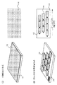
トランジスタを用いて形成される代表的な回路として、オペアンプや差動増幅回路等がある。ここで、図10(A)にカレントミラー回路を示し、図10(B)には前記カレントミラー回路の実際の基板上でのレイアウト例を示す。また図10(C)には差動増幅回路を示し、図10(D)には前記差動増幅回路の実際の基板上でのレイアウト例を示す。
【0005】
図10(A)に示すように、カレントミラー回路は、2つのトランジスタを有している。そして、トランジスタ201を流れるドレイン電流I1と、トランジスタ202を流れるドレイン電流I2とが等しいことが必要となる。つまり、カレントミラー回路においては、トランジスタ201とトランジスタ202との特性が等しいことが動作の前提となっている。その結果、両トランジスタの電気的特性にばらつきがある場合、I1=I2とは必ずしもならないため、回路として機能しない。よって、多くの場合において、カレントミラー回路を構成するトランジスタは、そのチャネル長やチャネル幅等が等しいものを用いて構成される。
【0006】
次いで、図10(C)に示すように、差動増幅回路は、カレントミラー回路を能動負荷として有している。この回路は、入力端(In1、In2)にそれぞれ異なる電位が与えられたとき、前述のカレントミラー回路によってI1=I2+I3となることを利用し、出力端(Out)より、In1、In2に入力された信号の電位差を増幅した波形を取り出すことが出来る回路である。この回路もまた、TFT211〜214の電気的特性が等しいことが前提となっている。
【0007】
つまり、図10(A)(B)に示したカレントミラー回路と、図10(C)(D)に示す差動増幅回路においては、構成する複数のTFTが素子整合性を有することが必要となる。しかし実際には、p-SiTFTは、半導体層に多数の結晶粒が集まって形成されており、それぞれの結晶状態は良好であっても、結晶粒同士の境界(粒界)においては配向が異なっているなどの理由で、電気的特性が劣ってしまう。つまり、p-SiTFTにおいてはこの粒界が活性層中に多く含まれており、さらに粒界の数や隣接した結晶粒同士の配向の違いにより、その電気的特性に差が生ずる場合がある。つまり、同じサイズのTFTを作製し、かつ各電極に同様な電圧を印加した場合にも、電流値等がばらついてしまう場合がある。
【0008】
本発明は、上記の問題点を鑑みてなされたものであり、前述のカレントミラー回路のように、複数のTFTが整合性を必要とする回路において、前記回路ごとの電気的特性のバラツキの影響を抑制した半導体装置を提供することを課題とする。
【0009】
【課題を解決するための手段】
本発明の半導体装置の作製方法は、
絶縁表面を有する基板上に非晶質半導体を形成し、
前記非晶質半導体を所望の形状にパターニングして、複数の第1の島状半導体を形成し、
複数の前記第1の島状半導体に線状に集光されたレーザ光を前記基板に対して相対的に走査しつつ照射し、複数の前記第1の島状半導体を結晶化し、
結晶化された複数の前記第1の島状半導体を所望の形状にパターニングして、複数の第2の島状半導体を形成し、
複数の前記第2の島状半導体を用いて複数のトランジスタを形成し、
複数の前記トランジスタのうち所定の数の前記トランジスタを用いて単位回路を形成する半導体装置の作製方法であって、
前記所定の数の前記トランジスタに用いられる前記第2の島状半導体は、それぞれ異なる前記第1の島状半導体から形成されることを特徴としている。
【0010】
本発明の半導体装置の作製方法は、
絶縁表面を有する基板上に非晶質半導体を形成し、
前記非晶質半導体上に金属含有層を形成し、熱処理により第1の結晶質半導体を形成し、
前記第1の結晶質半導体を所望の形状にパターニングして、複数の第1の島状半導体を形成し、
複数の前記第1の島状半導体に線状に集光されたレーザ光を前記基板に対して相対的に走査しつつ照射し、第2の結晶質半導体でなる複数の前記第1の島状半導体を形成し、
前記第2の結晶質半導体でなる複数の前記第1の島状半導体を所望の形状にパターニングして、複数の第2の島状半導体を形成し、
複数の前記第2の島状半導体を用いて複数のトランジスタを形成し、
前記複数のトランジスタのうち所定の数の前記トランジスタを用いて単位回路を形成する半導体装置の作製方法であって、
前記所定の数の前記トランジスタに用いられる前記第2の島状半導体は、それぞれ異なる前記第1の島状半導体から形成されることを特徴としている。
【0011】
【発明の実施の形態】
(実施の形態1)
本発明の一実施形態を、図3〜図5を用いて説明する。図3、4には、本発明の半導体装置の作製方法を示しており、図3(A)(B)、図4(A)(B)には、左側に斜視図、右側に上面図を示す。また図5(A)〜(F)には、本発明の半導体装置の作製方法を簡単に示している。
【0012】
基板101上に、半導体102を形成する(図3(A))。なお、基板101としては、半導体装置の作製を通じての処理温度に耐えうる材質のものであれば良く、例えば石英基板、シリコン基板、バリウムホウケイ酸ガラスあるいはアルミノホウケイ酸ガラス等の無アルカリガラス基板、金属基板の表面に絶縁膜を形成した基板等を用いることが出来る。また、処理温度に耐えうる程度の耐熱性を有するプラスチック基板であっても良い。
【0013】
なお、基板101と半導体102との間には、基板101に含まれるアルカリ金属等の不純物による半導体102の汚染を防ぐための下地膜を、絶縁膜等によって形成しても良い。また、半導体102は、公知の技術(スパッタ法、LPCVD法、プラズマCVD法等)を用いて成膜すれば良い。また、半導体102は、非晶質半導体であっても良いし、微結晶半導体、多結晶半導体であっても良い。
【0014】
続いて、半導体102をパターニングして、アライメントマーカー103と、第1の島状半導体104を形成する(図3(B))。なお本発明においては、前記基板101上には、複数個の第1の島状半導体104が並列に配置される。第1の島状半導体104は、先の尖った凸端部を1つ又は複数有する。そしてレーザ光は、前記1つ又は複数の凸端部から、それに対向する他端部にかけて走査される。つまり、第1の島状半導体104において、レーザ光は凸端部に最初に達する。そして本実施の形態では、前記凸端部をa点と称する。なお本発明では、複数個の第1の島状半導体は、縦方向には並列に配置される。さらに、横方向には複数の第1の島状半導体の凸端部(a点)が整列しないように、少しずらして配置される(図3(B))。なお、アライメントマーカー103、第1の島状半導体104の形状については、図3(B)に示す形状に限定しない。
【0015】
続いて、図4(A)に示すように、アライメントマーカー103を元に、レーザ照射位置を決定し、第1の島状半導体104にレーザ光106を照射することによって、第1の島状半導体104を結晶化する。ここで、第1の島状半導体を形成する半導体があらかじめある程度結晶化が進んでいる場合、このレーザ照射工程により、その結晶性がより高められる。ここでは、レーザ光はスリット(図示せず)によってエネルギー密度が低い領域を遮蔽し、この領域のレーザ光が半導体に当たらないようにしている。エネルギー密度の低いレーザ光が半導体に照射されて結晶化すると、その結晶粒は0.1[μm]程度もしくはそれ以下の微結晶粒となってしまい、そのような結晶性半導体では優れた電気的特性が得られないためである。エネルギー密度が十分か否かは、半導体において、所望の結晶粒が得られるか否かで判断され、設計者が適宜判断すれば良い。よって、設計者にとって結晶性が十分でないと判断される場合、そのときのエネルギー密度は低いと判断される。
【0016】
レーザ光のエネルギー密度は、スリットを介して得られたレーザ光スポットの端部近傍において低くなっているため、照射端部近傍においては結晶粒が小さく、結晶の粒界に沿って突起した部分(リッジ)が出現する。そのため、レーザ光スポットの軌跡(図4(A)に点線で表記)と、第1の島状半導体104が重ならないようにする。最低限、第1の島状半導体104より、後に形成される第2の島状半導体の領域(図4(A)、第1の島状半導体104中に点線で表記)が、前記レーザ光スポットの軌跡と重ならないようにする。
【0017】
なお、第1の島状半導体にレーザ照射を行う際、レーザ光スポットが第1の島状半導体の端部に達したときに、レーザ光スポットと第1の島状半導体とが、基板の表面もしくは裏面から見て1点で接するように、レーザ光の走査方向もしくは第1の島状半導体の形状を決定している。図4(A)において、第1の島状半導体104はそれぞれ凸端部(a点)で最初にレーザ光スポットと接する。このように、1つの接点よりレーザ光の照射が開始され、結晶化されると、当該接点を含めた近傍より(100)配向面を有する結晶が成長していく。よって最終的に、第1の島状半導体内では(100)配向面の率が高くなる。すなわち、各結晶粒が等しい配向面を有するため、粒界近傍での電子もしくはホールの移動がスムーズに行われ、よってこのような結晶性半導体は、大変良好な電界効果移動度を有する。
【0018】
本発明においては、第1の島状半導体104からは、複数の第2の島状半導体が形成される。本明細書では一例として、図3、4に示した第1の島状半導体104から3つの第2の島状半導体105が形成されるとする。そして、3つの前記第2の島状半導体105を凸端部(a点)に近い順に第2の島状半導体A、第2の島状半導体B、第2の島状半導体Cと称する。そうすると、第1の島状半導体104においては、凸端部(a点)から結晶化が開始されるため、第2の島状半導体A〜Cの結晶性は異なってしまう。言い換えると、第2の島状半導体の電気的特性は、凸端部(a点)からの距離に依存することになる。そこで本発明では、第2の島状半導体A〜Cから構成される回路特性のバラツキを抑制するために、以下のような手段を講じている。
【0019】
本発明では、複数個の第1の島状半導体は、縦方向には並列に配置される。また、横方向には複数の第1の島状半導体のa点が整列しないように、少しずらして配置される。そしてここでは仮に、それぞれ異なる第1の島状半導体から形成された3つの第2の島状半導体を用いて単位回路を形成されるとする。このような場合においては、前記3つの第1の島状半導体において、1つの第1の島状半導体からは第2の島状半導体Aに相当する部分、1つの第1の島状半導体からは第2の島状半導体Bに相当する部分、1つの第1の島状半導体からは第2の島状半導体Cに相当する部分が横方向に整列して配置されるようにする。
【0020】
なお本明細書において、単位回路とは、複数のトランジスタが電気的に接続された回路のことを示す。代表的には、複数のトランジスタが並列に接続され、且つ電気的に接続された回路のことを示す。そして例えば、アナログスイッチ、電流源、カレントミラー回路、差動増幅回路、オペアンプ回路などが単位回路に相当する。
【0021】
続いて、図4(B)に示すように、結晶化された第1の島状半導体104をパターニングすることによって、所望の形状の第2の島状半導体105を形成する。ここで、第2の島状半導体105は、第1の島状半導体の端部近傍を避け、良好な結晶性が得られている第1の島状半導体の中心近傍の領域を用いているのが望ましい。なお、マーカー103は、後の工程(ゲート電極形成、配線形成等)にて用いるマスクのアライメントに用いるために残しておいても良い。
【0022】
そして本発明では、3つの第1の島状半導体104において、1つの第1の島状半導体からは第2の島状半導体Aに相当する部分、1つの第1の島状半導体からは第2の島状半導体Bに相当する部分、1つの第1の島状半導体からは第2の島状半導体Cに相当する部分とを用いて単位回路を形成する。
【0023】
本発明では、単位回路を構成する複数の第2の島状半導体が、それぞれ異なる第1の島状半導体から形成される。そして、第2の島状半導体を3つ用いて単位回路を構成すると仮定すると、前記3つの第2の島状半導体は、それぞれが凸端部(a点)からの距離が異なるように設定する。そうすることによって、第2の島状半導体の特性バラツキを平均化することが出来る。その結果、単位回路ごとの特性の均一化をはかることが出来る。
【0024】
以上までの工程を簡単に図示したものを図5(A)〜(D)に示す。なお本発明では、第1の島状半導体302から複数の第2の島状半導体306が形成される。しかし、図5(A)〜(D)では簡単のため、第1の島状半導体302より、1つの第2の島状半導体306が形成された場合を示している。
【0025】
第2の島状半導体306では、ゲート電極307、ソース・ドレイン配線308、309がそれぞれ形成されて、TFTとなる。図5(E)において、A−A'における断面図を図5(F)に示す。
【0026】
本発明では、半導体に照射するレーザとして、公知のレーザを用いることが出来る。レーザは、パルス発振または連続発振の気体レーザもしくは固体レーザを用いることが出来る。気体レーザとして、エキシマレーザ、Arレーザ、Krレーザ等があり、固体レーザとして、YAGレーザ、YVO4レーザ、YLFレーザ、YALO3レーザ、ガラスレーザ、ルビーレーザ、アレキサンドライドレーザ、Ti:サファイアレーザ等が挙げられる。また、固体レーザとしては、Cr、Nd、Er、Ho、Ce、Co、NiまたはTmがドーピングされたYAG、YVO4、YLF、YALO3等の結晶を用いたレーザが適用される。当該レーザの基本波はドーピングする材料によって異なり、1[μm]前後の基本波を有するレーザ光が得られる。基本波に対する高調波は、非線形光学素子を用いることで得られる。さらに、固体レーザより発せられた赤外レーザ光を非線形光学素子でグリーンレーザ光に変換後、さらに別の非線形光学素子によって得られる紫外レーザ光を用いることが出来る。
【0027】
また本発明では、ビームスポットの幅は、第1の島状半導体または第2の島状半導体のサイズによって適宜変えることができる。例えば、電流を比較的多く流すことが望まれる駆動回路のTFTは、チャネル幅が大きく、よって第2の島状半導体のサイズも画素部に比べて大きい傾向にある。そこで、2通りのサイズの第1の島状半導体に、スリットの幅を変えてレーザ光を走査する場合について図11を用いて説明する。
【0028】
図11(A)に、走査方向と垂直な方向における第1の島状半導体の長さが短い場合を、図11(B)に走査方向と垂直な方向における第1の島状半導体の長さが長い場合の、レーザ光の走査する部分と、第1の島状半導体との関係を示す。
【0029】
図11(A)におけるスポット1901の幅をW1、図11(B)におけるスポット1902の幅をW2とすると、W1<W2となる。もちろん、スポットの幅はこれに限られず、第1の島状半導体の間の走査方向と垂直な方向における間隔に余裕がある場合は、自由にその幅を設定することができる。
【0030】
なお本発明では、図11(A)(B)に示すように、レーザ光を基板全面に照射するのではなく、第1の島状半導体の部分を最低限結晶化できるようにスポットを走査する。基板全面を照射するのではなく、第1の島状半導体が結晶化できるように必要最低限の部分にレーザ光が照射されるので、1枚の基板にかかる処理時間を抑えることができ、基板処理の効率を高めることができる。
【0031】
(実施の形態2)
本実施の形態では、実施の形態1とは異なる実施の形態として、グラフォエピタキシの原理を応用した半導体装置の作製方法について、図1、2を用いて説明する。
【0032】
グラフォエピタキシの基本原理は、育成する結晶の持っている表面エネルギーの異方性を利用したものである。なお表面エネルギーの異方性とは、例えば、塩の結晶を溶液から成長させると正六面体になる性質のことを指し、SOI構造の場合では、SiO2とSiとの界面エネルギーの異方性となることを指す。
【0033】
図1(A)において、10は基板である。基板10は、半導体装置の作製を通じての処理温度に耐えうる材質のものであれば良く、例えば石英基板、シリコン基板、バリウムホウケイ酸ガラスあるいはアルミノホウケイ酸ガラス等の無アルカリガラス基板、金属基板の表面に絶縁膜を形成した基板等を用いることが出来る。また、処理温度に耐えうる程度の耐熱性を有するプラスチック基板であっても良い。
【0034】
次いで、基板10上に絶縁膜11を形成する。絶縁膜11は、酸化珪素膜、窒化珪素膜又は酸化窒化珪素膜などの絶縁膜から形成される。図1(B)に示すように、絶縁膜11は規則的な凸凹のパターンが形成されるようにする。言い換えると、絶縁膜11は、規則的に凹部と凸部とが繰り返される形状にする。
【0035】
続いて、絶縁膜11上に半導体膜12を形成する。半導体膜12は、凸凹の形状を有する絶縁膜11上に形成される。その結果、図1(C)に示すように、半導体膜12も凸凹の形状を有する。
【0036】
上記のような状態において、半導体膜12にレーザ光を照射する。そうすると、半導体膜12は、図1(C)に示すような面配向を有する結晶を形成する。より具体的には、基板10の表面に対して垂直な溝を形成すると、溝の側面と底面または上面とにSiが接するため、それぞれの面に接するSiの(100)面およびそれと等価の(010)、(001)面が接するように再配列する。このため、基板と垂直な方位および平行な面内方位とが揃った単結晶が成長することになる。
【0037】
なお本実施の形態の半導体装置の作製方法は、実施の形態1において図3〜図5を用いて説明した半導体装置の作製方法と組み合わせてもよい。そのときには、図2(A)に示すように、基板10上に凸凹形状の絶縁膜11を形成し、前記絶縁膜11上に半導体膜を形成して、所望の形状にパターニングして島状半導体層12を形成する。そして、島状半導体層12の凸端部(先端)から最初にレーザ光スポットが照射されるようにする。そうすると、島状半導体層12の凸端部(先端)から結晶化がはじまるために、さらに特性の良い島状半導体層を得ることが出来る。
【0038】
また、絶縁膜11の形状は、図2(A)に示すように凸凹形状に限定されない。例えば、図2(B)に示すような三角形状でもかまわない。
【0039】
グラフォエピキタシの原理を応用した半導体装置の作製方法の工程を簡単に示したものを図23、24に示す。
【0040】
図23(A)において、最初に基板31上に下地膜32を形成する。基板31としては、半導体装置の作製を通じての処理温度に耐えうる材質のものであれば良く、例えば石英基板、シリコン基板、バリウムホウケイ酸ガラスあるいはアルミノホウケイ酸ガラス等の無アルカリガラス基板、金属基板の表面に絶縁膜を形成した基板等を用いることが出来る。また、処理温度に耐えうる程度の耐熱性を有するプラスチック基板であっても良い。
【0041】
次いで、基板31上に下地膜32を形成する。下地膜32は、酸化珪素膜、窒化珪素膜又は酸化窒化珪素膜などの絶縁膜から形成される。このとき、下地膜32は、図23(A)に示すように規則的な凸凹のパターンが形成されるようにする。
【0042】
そして、下地膜32上に半導体膜33を形成する。半導体膜33は、凸凹の形状を有する下地膜32上に形成される。その結果、図23(B)に示すように、半導体膜33の表面も凸凹の形状を有する。
【0043】
続いて、半導体膜33にレーザ光35を照射する。そうすると、結晶化された半導体膜34が形成される(図23(C))。
【0044】
次いで、半導体膜34を所望の形状にパターニングを行うと、島状半導体層36が形成される(図24(A))。そして、前記島状半導体層36に、ゲート配線37、ソース・ドレイン配線38、層間絶縁膜39を形成する(図24(B))。
【0045】
本実施の形態は、実施の形態1と任意に組み合わせることが可能である。
【0046】
(実施の形態3)
本実施の形態では、実施の形態1、2において説明した半導体装置の作製方法を用いて形成した島状半導体層にゲート電極とソース・ドレイン配線とを形成したときの上面図について、図6〜9を用いて説明する。
【0047】
図6において、1は第1の島状半導体層であり、2および4はソース配線及びドレイン配線の一方に相当する。3はゲート電極であり、5はコンタクトホールであり、6A〜6Cは第2の島状半導体層に相当する。
【0048】
そして第1の島状半導体層1からは、3つの第2の島状半導体層6A〜6Cが形成されるが、本明細書では前記3つの第1の島状半導体層をa点に近い順に第2の島状半導体層6A、第2の島状半導体層6B、第2の島状半導体層6Cと称する。そして本発明では、図6に示すように、3つの第1の島状半導体層1において、第2の島状半導体層6Aと、第2の島状半導体層6Bと、第2の島状半導体層6Cとを用いて回路を形成する。
【0049】
本発明では、単位回路を構成する複数の第2の島状半導体が、それぞれ異なる第1の島状半導体から形成される。そして、第2の島状半導体を3つ用いて単位回路を構成すると仮定すると、前記3つの第2の島状半導体は、それぞれが凸端部(a点)からの距離が異なるように設定する。そうすることによって、第2の島状半導体の特性バラツキを平均化することが出来る。その結果、単位回路ごとの特性の均一化をはかることが出来る。
【0050】
また、図7には、3つの第2の島状半導体層を用いてマルチチャネル型のTFTを形成した場合を示す。第2の島状の半導体層6Dは、図4において、第2の島状半導体層6A〜6Cが合体したような構成を有する。図7に示すようなマルチチャネル型のTFTは、図10(A)に示したカレントミラー回路に用いることが好ましい。
【0051】
次いで、図8には、1つの第2の島状半導体層を用いてTFTを形成した場合であって、且つ複数の第1の島状半導体層1が分離されている場合を示す。
【0052】
最後に、図9には、図6〜8に示した半導体装置の回路図を示す。
【0053】
本実施の形態は、実施の形態1、2と任意に組み合わせることが可能である。
【実施例】
以下に、本発明の実施例について記載する。
【0054】
[実施例1]
本実施例においては、CWレーザを用いたレーザ結晶化工程の一例について述べる。
【0055】
本方法に適当なCWレーザとしては、波長が550[nm]以下で出力安定性の著しく高いものが望ましい。例えば、YVO4レーザの第2高調波や、YAGレーザの第2高調波、YLFレーザの第2高調波、ガラスレーザの第2高調波、YAlO3レーザの第2高調波、Arレーザ等が該当する。あるいは、前記レーザのさらなる高次高調波を用いても良い。あるいは、ルビーレーザ、アレキサンドライドレーザ、Ti:サファイアレーザ、連続発振のエキシマレーザ、Krレーザ、CO2レーザ、連続発振のヘリウムカドミウムレーザ、銅蒸気レーザ、金蒸気レーザ等のレーザを使用しても良い。さらに、これらのレーザを複数、あるいは複数種用いることも可能である。
【0056】
図12(A)は、CWレーザ結晶化を行うための装置を模式的に表したものであり、レーザ発振器701、ミラー702、凸レンズ703、X−Yステージ704等からなる。ここで用いるレーザは、出力10[W]で連続発振のYVO4レーザである。レーザ発振器701には、非線形光学素子が内蔵されており、射出口より第2高調波が射出される。
【0057】
レーザ発振器701から射出されたレーザビームは、図12(A)中、Aで示すように円形状をしている。前記レーザビームは水平方向に射出され、ミラー702によって鉛直方向から20°前後の方向に偏向される。その後、水平方向に配置された凸レンズ703により集光される。X−Yステージ704に基板705を固定し、基板上に形成された半導体層上の照射面を、凸レンズ703の焦点に合わせる。このとき、照射面が凸レンズ703と平行になるように配置する。すなわち基板705は水平配置される。凸レンズ703には、20°前後の角度でレーザビームが入射するため、凸レンズの非点収差によって、照射面でのレーザビーム光の形状は楕円形状となる。照射面におけるビーム形状は、凸レンズ703への入射角度によって決定するため、凸レンズに対し、鉛直方向により大きな角度を持ってレーザビームを入射させることによって、さらにアスペクト比の大きい楕円とすることが出来るが、反面、焦点深度が浅くなるために均一な照射が困難となることから、偏向角度は20°前後が妥当であるとしている。
【0058】
基板全面の半導体層を結晶化するためには、適当な照射ピッチで楕円ビームをその長径方向にずらしながら基板上を走査させることを繰り返す必要がある。この動作は、レーザ発振器701、ミラー702、凸レンズ703からなるレーザ出力部分を固定し、X−Yステージ704を用いて、基板上を楕円ビームが走査するように基板を移動させて行う。照射対象である基板のサイズが、図12(A)においてX方向600[mm]、Y方向720[mm]であるとし、楕円ビームの長軸長さが200[μm]であるとき、図12(A)に示す方向で走査すると、3000回(1500往復)の走査によって、基板全面にレーザ照射を行うことが出来る。
【0059】
また、後の実施例で詳しく説明するが、レーザ発振器を複数台用い、楕円ビームを長軸方向に複数並べて平行に走査することにより、走査回数を減らし、処理時間を短縮することも可能である。こうすることにより、単体レーザ光の両端部における、エネルギー密度の低い部分が隣接間で互いに重なり合い、エネルギー密度を高くすることが出来る。よって、有効照射領域を広く、かつ1回の照射領域における有効照射領域の割合を大きくすることが出来、回路レイアウトの際の制約をより小さくすることも出来る。
【0060】
本実施例は、実施の形態1〜実施の形態3と自由に組み合わせて実施することが可能である。
【0061】
[実施例2]
本実施例においては、実施例1とは異なる光学系を用いてレーザビームの偏光を行う例について、図12(B)に沿って説明する。
【0062】
レーザ発振器801から射出されたレーザビームは、図12(B)中、Aで示すように円形状をしている。前記レーザビームは水平方向に射出され、ミラー802によって鉛直方向に偏向される。その後、第1のシリンドリカルレンズ803によってX方向に集光される。このときのビーム形状は、図12(B)中、Bで示すように、円形状がX方向に集光されて、Y方向を長軸とする楕円形状となる。続いて、第2のシリンドリカルレンズ804によってY方向に集光される。このときのビーム形状は、図12(B)中、Cで示すように、さらにY方向に集光されて、X方向を長軸とする楕円形状となる。このような光学系を用いると、実施例2で示したよりもさらにアスペクト比の大きい楕円形状のビームを得ることが出来る。その後、X−Yステージ805に固定された基板806に照射される。基板上のレーザビームの走査については、実施例3と同様にして行えばよい。
【0063】
また、レーザ発振器を複数台用い、楕円ビームを長軸方向に複数並べて平行に走査することにより、走査回数を減らし、処理時間を短縮することも可能である。こうすることにより、単体レーザ光の両端部における、エネルギー密度の低い部分が隣接間で互いに重なり合い、エネルギー密度を高めることが出来る。よって、有効照射領域を広くすることが出来、より回路レイアウトに制約を与えないようにすることも出来る。
【0064】
本実施例は、実施の形態1〜実施の形態3、実施例1と自由に組み合わせて実施することが可能である。
【0065】
[実施例3]
CWレーザによって、実施形態に示した工程に従って半導体層を結晶化する場合、単体のレーザ発振器より発振されるレーザ光の、被照射面における形状は、楕円形状もしくは矩形状である。また、照射面でのエネルギー密度を高めるためにレーザ光をスポット状に絞り込んでいるため、その照射範囲は図13(A)に示すようになる。
【0066】
スポット状に絞り込んだレーザ光の中では、さらにエネルギー密度に分布がある。図13(A)において、長軸方向、X断面すなわち楕円の長軸方向におけるエネルギー分布を図13(B)に示す。
【0067】
図13(B)に示すように、レーザ光スポットの中では、中心部から端部に向かって徐々にエネルギー密度が減少する分布を有する。ここで、Eと示しているのは、半導体層を良好に結晶化させるために最低限必要なエネルギー密度とする。すると、図13(C)において、Dで示した範囲のレーザ光が照射された半導体層は良好に結晶化し、優れた電気的特性を有する。反面、dで示した範囲のレーザ光が照射された半導体層は、レーザ光のエネルギー密度が十分でないために溶融が十分でなく、微結晶化する。このような領域においては十分な電気的特性が得られないため、活性層として用いるには適さない。
【0068】
本発明のように、複数のTFTを1つの第1の島状半導体層をパターニングして得られる半導体層を用いて作製するには、Dで示した範囲がより広いことが望ましい。しかしレーザ光スポット径を大きくするには限度があるため、その限られた幅で回路を構成しようとすると、素子のレイアウトが困難になる。結果として配線等の引き回しが長くなり、非効率な回路レイアウトとなってしまう。
【0069】
そこで本実施例においては、複数のレーザ発振器から出力されるレーザ光を用いて、効率的なレーザ照射を行う方法の一例について説明する。
【0070】
図13(D)を参照する。401〜403は、それぞれ異なる3台のレーザ発振器より出力されたレーザ光を、光学系を用いてスポット状に集光したものである。各レーザ光スポット401〜403は、各楕円の長軸が直線上に並び、かつ互いのレーザ光スポットの一部が重なることによって合成され、1つのレーザ光スポットとなっている。
【0071】
図13(E)に、各レーザ光スポット401〜403の、長軸方向のエネルギー密度分布を404〜406で示す。各スポットのエネルギー密度は等しく、そのピーク値はE0で表される。合成されたレーザ光スポットにおいては、重なり合う領域のエネルギー密度は加算され、図13(E)に407で示したようなエネルギー密度分布となる。
【0072】
このとき、隣接したスポット404、405が重なり合う領域と、405、406が重なり合う領域においては、2つのスポットのエネルギー密度が加算され、半導体層を良好に結晶化させるのに十分なエネルギー密度を有する。よって、合成後のスポット形状は、図13(F)に408で示す形状となり、この中で半導体層を良好に結晶化させることの出来る範囲はD0となる。
【0073】
なお、隣接したスポットの重なり合う領域におけるエネルギー密度の和は、単体スポットのピーク値E0に等しくなるのが理想であるが、D0の範囲で半導体層を良好に、かつ均一に結晶化できる範囲の値となるように、適宜スポットの重なり幅を設定すれば良い。
【0074】
図13(D)(F)からわかるように、複数のレーザ光スポットを重ね合わせてエネルギー密度の低い部分を互いに補うようにすることで、より広い幅でのレーザ照射が可能となる。
【0075】
なお、合成レーザ光スポットの使用は、単に広い領域の走査を可能とするだけでなく、効率面でも有利である。単独のレーザ光を用いた場合の照射領域の幅は(D+2d)であり、図13(F)に示したような合成レーザ光スポットを用いた場合の照射領域の幅は(D0+2d)である。レーザ光スポット1走査幅あたり、良好な結晶化が行える幅の比は、前者は(D/(D+2d))であり、後者は(D0/(D0+2d))となる。D<D0であるから、より効率良く、良好な結晶化を行うことが出来るといえる。
【0076】
また、合成レーザ光スポットにおいて、長軸方向の両端に位置する、エネルギー密度の低い領域を、図13(G)に示すように、スリット409を用いて遮蔽し、半導体層に当たらないようにするとより望ましい。このとき、半導体層表面でのスポット形状は、図13(H)に示すようになり、長軸方向にD1(<D0)の幅を有する、矩形に近い形状となる。
【0077】
このような形状で半導体層に照射されるレーザ光スポットにおいては、そのスポットにおいて、エネルギー密度の低い領域が存在しない。もしくは存在しても、スリットを用いていない場合と比較してはるかに幅が小さいので、レーザ光スポットの照射端部が第1の島状半導体層上を走査しないようにスポット位置を制御するのがより容易になる。よって、レーザ光の走査経路および、第1の島状半導体層または第2の島状半導体層のレイアウト時の制約を小さくすることが出来る。
【0078】
さらに、スリットを用いることで、レーザ発振器の出力を止めることなく、エネルギー密度を一定に保ったままでレーザ光スポットの幅を変更することが出来るため、レーザ光スポットの照射端部が第2の島状半導体層もしくはそのチャネル形成領域を走査するのを防ぐことが出来る。また、基板上の不必要な領域にもレーザ光を照射して、基板にダメージが与えられるのを防ぐ効果も期待できる。
【0079】
本実施例は、実施の形態1〜実施の形態3、実施例1、2と自由に組み合わせて実施することが可能である。
【0080】
[実施例4]
本発明において用いられるレーザ照射装置の制御系を含めた構成について、図14(A)を用いて説明する。901はレーザ発振器である。図14(A)では3つのレーザ発振器を用いているが、レーザ照射装置が有するレーザ発振器はこの数に限定されない。
【0081】
図14(A)のレーザ照射装置は、中央演算処理装置及びメモリ等の記憶手段を兼ね備えたコンピュータ908を有している。コンピュータ908は、レーザ発振器901の発振を制御し、なおかつレーザ光スポットがマスクのパターン情報に従って定められる領域を覆うように、基板906へのレーザ光スポットの照射位置を制御すべく、基板を所定の位置に移動させることができる。
【0082】
なお、レーザ発振器901は、チラー902を用いてその温度を一定に保つようにしても良い。チラー902は必ずしも設ける必要はないが、レーザ発振器901の温度を一定に保つことで、出力されるレーザ光のエネルギーが温度によってばらつくのを抑えることができる。
【0083】
また904は光学系であり、レーザ発振器901から出力された光路を変更したり、そのレーザ光スポットの形状を加工したりして、レーザ光を集光することができる。さらに、図14(A)のレーザ照射装置では、光学系904によって、複数のレーザ発振器901から出力されたレーザ光スポットを互いに一部を重ね合わせることで、合成することができる。
【0084】
なお、レーザ光を一次的に完全に遮蔽することができるAO変調器903を、被処理物である基板906とレーザ発振器901との間の光路に設けても良い。また、AO変調器903の代わりに、テニュエイター(光量調整フィルタ)を設けて、レーザ光のエネルギー密度を調整するようにしても良い。
【0085】
また、被処理物である基板906とレーザ発振器901との間の光路に、レーザ発振器901から出力されたレーザ光のエネルギー密度を測定する手段(エネルギー密度測定手段)910を設け、測定したエネルギー密度の経時変化をコンピュータ908において監視するようにしても良い。この場合、レーザ光のエネルギー密度の減衰を補うように、レーザ発振器901からの出力を高めるようにしても良い。
【0086】
合成されたレーザ光スポットは、スリット905を介して被処理物である基板906に照射される。スリット905は、レーザ光を遮ることが可能であり、なおかつレーザ光によって変形または損傷しないような材質で形成するのが望ましい。そして、スリット905はスリットの幅が可変であり、当該スリットの幅によってレーザ光スポットの幅を変更することができる。
【0087】
なお、スリット905を介さない場合の、レーザ発振器901から発振されるレーザ光の基板906におけるレーザ光スポットの形状は、レーザの種類によって異なり、また光学系により成形することもできる。
【0088】
基板906はX−Yステージ907上に載置されている。図14(A)では、X−Yステージ907は、コンピュータによって制御され、被処理物すなわち基板906を移動することによってレーザ光スポットの照射位置を制御している。
【0089】
さらに本発明では、コンピュータ908によって、スリット905の幅を制御し、マスクのパターン情報に従ってレーザ光スポットの幅を変更することができる。
【0090】
さらに図14(A)のレーザ照射装置は、被処理物の温度を調節する手段を備えていても良い。また、レーザ光は指向性およびエネルギー密度の高い光であるため、ダンパーを設けて、反射光が不適切な箇所に照射されるのを防ぐようにしても良い。ダンパーは、反射光を吸収させる性質を有していることが望ましく、ダンパー内に冷却水を循環させておき、反射光の吸収により隔壁の温度が上昇するのを防ぐようにしても良い。また、X−Yステージ907に基板906を加熱するための手段(基板加熱手段)を設けるようにしても良い。
【0091】
なお、アライメントマーカーをレーザで形成する場合、マーカー用のレーザ発振器を設けるようにしても良い。この場合、マーカー用のレーザ発振器の発振を、コンピュータ908において制御するようにしても良い。さらにマーカー用のレーザ発振器を設ける場合、マーカー用のレーザ発振器から出力されたレーザ光を集光するための光学系を別途設ける。なおマーカーを形成する際に用いるレーザは、代表的にはYAGレーザ、CO2レーザ等が挙げられるが、もちろんこの他のレーザを用いて形成することは可能である。
【0092】
またマーカーを用いた位置合わせのために、CCDカメラ909を1台、場合によっては数台設けるようにしても良い。
【0093】
なお、マーカーを設けずに、CCDカメラ909によって第1の島状半導体層のパターンを認識し、位置合わせを行うようにしても良い。この場合、コンピュータ908に入力されたマスクによる第1の島状半導体層のパターン情報と、CCDカメラ909において収集された実際の第1の島状半導体層のパターン情報とを照らし合わせて、基板の位置情報を把握することができる。この場合マーカーを別途設ける必要がない。
【0094】
なお、図14(A)では、レーザ発振器を複数台設けたレーザ照射装置の構成について示したが、レーザ発振器は1台であってもよい。図14(B)に、レーザ発振器を1台用いたレーザ照射装置の構成を示す。図14(B)において、901はレーザ発振器、902はチラーである。また910はエネルギー密度測定装置、903はAO変調器、904は光学系、905はスリット、909はCCDカメラである。基板906はX−Yステージ907上に設置され、レーザ光スポットの基板906への照射位置が制御されている。そして図9(A)に示したものと同様に、コンピュータ908によって、レーザ照射装置が有する各手段の動作が制御されている。図14(A)と異なるのはレーザ発振器が1つであることである。したがって、光学系904もまた図9(A)の場合と異なり、1つのレーザ光を集光する機能を有していれば良い。
【0095】
図15(A)に、レーザ光を1回照射する場合の、半導体膜のパターニングのマスクの形状と、レーザ光スポット2001の幅の関係を一例として示す。2002は、4つのレーザ発振装置から出力されたレーザ光を重ね合わせて合成することで得られる幅W3のビームスポットを走査した部分、2001は、3つのレーザ発振装置から出力されたレーザ光を重ね合わせて合成することで得られる幅W4のビームスポットを走査した部分である。走査幅は、スリットによって制御しても良いし、一部のレーザ光の出力を停止、もしくはAO変調器を用いて遮蔽しても良い。
【0096】
なお本実施例のように、AO変調器を用いることで、全てのレーザ発振装置の出力を止めずにレーザ光スポット2001の幅を自在に変えることができ、レーザ発振装置の出力を止めることで出力が不安定になるのを避けることができる。
【0097】
上記構成により、レーザ光の軌跡の幅を変えることができるので、図15(A)に示すように部分的に第1の島状半導体層の幅が異なっていても、レーザ光の軌跡のエッジが、パターニングによって得られる半導体と重なるのを防ぐことができる。また、また不必要な部分にレーザ光を照射することで基板に与えられるダメージをさらに軽減することができる。
【0098】
次に、レーザ光照射の途中で、AO変調器によりレーザ光を遮り、所定の部分にのみレーザ光を照射する例について説明する。なおーザー光を遮蔽しているが、本発明はこれに限定されず、レーザ光を遮蔽できればどのような手段を用いても良い。
【0099】
本発明では、コンピュータにおいて、入力されたマスクの情報に基づきレーザ光を走査する部分を把握する。さらに本実施例では、走査するべき部分のみにレーザ光が照射されるようにAO変調器を用いてレーザ光を遮る。このときAO変調器は、レーザ光を遮ることが可能であり、なおかつレーザ光によって変形または損傷しないような材質で形成するのが望ましい。
【0100】
図15(B)に、半導体膜のパターニングのマスクの形状と、レーザ光が照射される部分の関係を一例として示す。2001は、レーザ光スポットを示しており、2004は、レーザ光が照射された部分を示している。図15(B)に示すとおり、第1の島状半導体層が形成されていない部分を走査するときには、AO変調器によってレーザ光が遮蔽され、基板上に照射されていない。本実施例では結晶化させる必要のない部分にはレーザ光を照射しないか、照射されていてもそのエネルギー密度が低くなるようにすることができる。したがって、不必要な部分にレーザ光を照射することで基板に与えられるダメージをさらに軽減することができる。
【0101】
本実施例は、実施の形態1〜実施の形態3、実施例1〜実施例3と自由に組み合わせて実施することが可能である。
【0102】
[実施例5]
本実施例においては、本発明の半導体装置の作製方法における工程フローについて説明する。
【0103】
図16(A)に、工程フローを示す。まずCADを用いて半導体装置の回路設計を行う。回路レイアウト、すなわちTFTの配置が決定すると、第2の島状半導体層の形成場所も決定する。このとき、1つの第1の島状半導体層に含まれる第2の島状半導体層は、チャネル形成領域における電荷の移動方向を、レーザ光の走査方向と平行もしくはそれに準ずる方向に揃えるようにすることが望ましいが、用途に応じて意図的に方向を揃えない様にしても良い。
【0104】
また、このとき第1の島状半導体層と共にマーカーが形成されるように、第1の島状半導体層のマスクを設計するようにしても良い。
【0105】
そして、設計された第1の島状半導体層のマスクの形状に関する情報(パターン情報)を、レーザ照射装置が有するコンピュータに入力する。コンピュータでは、入力された第1の島状半導体層のパターン情報に基づき、走査方向に対して垂直方向における、各第1の島状半導体層の幅を算出する。そして、各第1の島状半導体層の幅をもとに、走査方向に対して垂直方向におけるスリットの幅を設定する。
【0106】
そして、スリットの幅をもとに、マーカーの位置を基準として、レーザ光の走査経路を定める。
【0107】
一方、半導体層基板上に成膜し、第1の島状半導体層のマスクを用いて当該半導体層をパターニングし、第1の島状半導体層を形成する。そして第1の島状半導体層が形成された基板を、レーザ照射装置のステージに設置する。
【0108】
そしてマーカーを基準にして、定められた走査経路にしたがってレーザ光を照射し、第1の島状半導体層を注目して結晶化する。
【0109】
そして、レーザ光を照射した後、レーザ光照射により結晶性が高められた第1の島状半導体層をパターニングし、第2の島状半導体層を形成する。以下、第2の島状半導体層からTFTを作製する工程が行われる。TFTの具体的な作製工程はTFTの形状によって異なるが、代表的にはゲート絶縁膜を成膜し、第2の島状半導体層に不純物領域を形成する。そして、ゲート絶縁膜及びゲート電極を覆うように層間絶縁膜を形成し、当該層間絶縁膜にコンタクトホールを開口し、不純物領域の一部を露出させる。そして当該コンタクトホールを介して不純物領域に接するように層間絶縁膜上に配線を形成する。
【0110】
次に、アライメントマーカーを形成することなく、CCDカメラによって基板とマスクのアライメントを行う例について説明する。
【0111】
図16(B)に、工程フローを示す。まず図16(A)の場合と同様に、CADを用いて半導体装置の回路設計を行う。回路レイアウト、すなわちTFTの配置が決定すると、第2の島状半導体層の形成場所も決定する。このとき、1つの第1の島状半導体層に含まれる第2の島状半導体層は、チャネル形成領域における電荷の移動方向を、レーザ光の走査方向と平行もしくはそれに準ずる方向に揃えるようにすることが望ましいが、用途に応じて意図的に方向を揃えない様にしても良い。
【0112】
そして、設計された第1の島状半導体層のマスクの形状に関する情報(パターン情報)を、レーザ照射装置が有するコンピュータに入力する。コンピュータでは、入力された第1の島状半導体層のパターン情報に基づき、走査方向に対して垂直方向における、各第1の島状半導体層の幅を算出する。そして、各第1の島状半導体層の幅をもとに、走査方向に対して垂直方向におけるスリットの幅を設定する。
【0113】
一方、半導体層を基板上に成膜し、第1の島状半導体層のマスクを用いて当該半導体層をパターニングし、第1の島状半導体層を形成する。そして第1の島状半導体層が形成された基板を、レーザ照射装置のステージに設置する。
【0114】
そして、ステージに設置された基板上の第1の島状半導体層のパターン情報を、CCDカメラにより検出し、コンピュータに情報として入力する。コンピュータではCADによって設計された第1の島状半導体層のパターン情報と、CCDカメラによって得られる、実際に基板上に形成された第1の島状半導体層のパターン情報とを照らし合わせ、基板とマスクとの位置合わせを行う。
【0115】
また該スリットの幅と、CCDカメラによる第1の島状半導体層の位置情報とをもとに、レーザ光の走査経路を決定する。
【0116】
そして、定められた走査経路にしたがってレーザ光を照射し、第1の島状半導体層を狙って結晶化する。
【0117】
次に、レーザ光を照射した後、結晶性が高められた第1の島状半導体層をパターニングし、第2の島状半導体層を形成する。以下、第2の島状半導体層からTFTを作製する工程が行われる。TFTの具体的な作製工程はTFTの形状によって異なるが、代表的にはゲート絶縁膜を成膜し、第2の島状半導体層に不純物領域を形成する。そして、ゲート絶縁膜及びゲート電極を覆うように層間絶縁膜を形成し、当該層間絶縁膜にコンタクトホールを開口し、不純物領域の一部を露出させる。そして当該コンタクトホールを介して不純物領域に接するように層間絶縁膜上に配線を形成する。
【0118】
次に、レーザ光の照射を複数回行う例について説明する。ここでは、例として1度レーザ照射を行った後、方向を変えて2度目のレーザ照射を行う工程を挙げる。
【0119】
図17(A)に、工程フローを示す。まずCADを用いて半導体装置の回路設計を行う。回路レイアウト、すなわちTFTの配置が決定すると、第2の島状半導体層の形成場所も決定する。このとき、1つの第1の島状半導体層に含まれる第2の島状半導体層は、チャネル形成領域における電荷の移動方向を、レーザ光の走査方向と平行もしくはそれに準ずる方向に揃えるようにすることが望ましいが、用途に応じて意図的に方向を揃えない様にしても良い。
【0120】
そして、設計された第1の島状半導体層のマスクの形状に関する情報(パターン情報)を、レーザ照射装置が有するコンピュータに入力する。コンピュータでは、入力された第1の島状半導体層のパターン情報に基づき、2つの各走査方向それぞれに対して垂直方向における、各第1の島状半導体層の幅を2通り算出する。そして、各第1の島状半導体層の幅をもとに、2つの各走査方向に対して垂直方向におけるスリットの幅をそれぞれ算出する。
【0121】
そして、2つの各走査方向において、それぞれ定められたスリットの幅をもとに、マーカーの位置を基準として、レーザ光の走査経路を定める。
【0122】
一方、半導体層を基板上に成膜し、第1の島状半導体層のマスクを用いて該半導体層をパターニングし、第1の島状半導体層を形成する。そして第1の島状半導体層が形成された基板を、レーザ照射装置のステージに設置する。
【0123】
そしてマーカーを基準にして、定められた2つの走査経路のうち、第1の走査経路にしたがって第1のレーザ光を照射し、第1の島状半導体層を狙って結晶化する。
【0124】
そして、走査方向を変え、第2の走査経路にしたがって、第2のレーザ光を照射し、第1の島状半導体層を狙って結晶化する。
【0125】
なお、1回目のレーザ光の走査方向と2回目のレーザ光の走査方向の角度は、予めメモリ等に記憶しておいても良いし、手動でその都度入力するようにしても良い。
【0126】
なお図17(A)では、同じ第1の島状半導体層に2回レーザー光を照射する例について示したが、AO変調器等を用いることで、場所指定して走査方向を変えることも可能である。例えば信号線駆動回路における走査方向と画素部及び走査線駆動回路における走査方向とを異ならせ、AO変調器を用いて信号線駆動回路となる部分においてレーザ光を照射する場合は、AO変調器を用いて画素部及び走査線駆動回路となる部分においてレーザ光が照射されないようにし、画素部及び走査線駆動回路となる部分においてレーザ光を照射する場合は、AO変調器を用いて信号線駆動回路となる部分においてレーザ光が照射されないようにすることができる。そしてこの場合、コンピュータにおいてAO変調器を位置制御手段と同期させるようにする。
【0127】
なお、レーザ光を照射した後、結晶性が高められた第1の島状半導体層をパターニングし、第2の島状半導体層を形成する。以下、第2の島状半導体層からTFTを作製する工程が行われる。TFTの具体的な作製工程はTFTの形状によって異なるが、代表的にはゲート絶縁膜を成膜し、第2の島状半導体層に不純物領域を形成する。そして、ゲート絶縁膜及びゲート電極を覆うように層間絶縁膜を形成し、当該層間絶縁膜にコンタクトホールを開口し、不純物領域の一部を露出させる。そして当該コンタクトホールを介して不純物領域に接するように層間絶縁膜上に配線を形成する。
【0128】
比較対象のために、図17(B)に従来の半導体装置の工程フローを示す。図17(B)に示すように、CADによる半導体装置のマスク設計が行われる。一方で、基板に非晶質半導体層を成膜し、当該非晶質半導体層が成膜された基板をレーザ照射装置に設置する。そして、非晶質半導体層全面にレーザ光が照射されるように走査し、非晶質半導体層を結晶化させる。そして、結晶化により得られた多結晶半導体層にアライメントマーカーを形成し、当該アライメントマーカーを基準として多結晶半導体層をパターニングして第2の島状半導体層を形成する。そして当該第2の島状半導体層を用いてTFTを作製する。
【0129】
このように本発明では、図17(B)に示すような従来の場合とは異なり、アライメントマーカーをレーザ光を用いて非晶質半導体層を結晶化させる前に形成する。そして、半導体層のパターニングのマスクの情報に従って、レーザ光を走査させる。
【0130】
上記構成により、基板上の半導体層のうち、パターニングにより除去される部分にレーザ光を照射する時間を省くことができるので、レーザ光照射にかかる時間を短縮化することができ、なおかつ基板の処理速度を向上させることができる。
【0131】
なお、レーザ光による結晶化工程の前に、触媒を用いて半導体層を結晶化させる工程を含んでいても良い。触媒元素を用いる場合、特開平7−130652号公報、特開平8−78329号公報で開示された技術を用いることが望ましい。
【0132】
触媒を用いて半導体層を結晶化させる工程を含んでいる場合、非晶質半導体層を成膜後にNiを用いて結晶化させる工程(NiSPC)を含んでいる。例えば特開平7−130652号公報に開示されている技術を用いる場合、重量換算で10[ppm]のニッケルを含む酢酸ニッケル塩溶液を非晶質半導体層に塗布してニッケル含有層を形成し、500℃、1時間の脱水素工程の後、500〜650[℃]で4〜12時間、例えば550[℃]、8時間の熱処理を行い結晶化する。尚、使用可能な触媒元素は、ニッケル(Ni)の以外にも、ゲルマニウム(Ge)、鉄(Fe)、パラジウム(Pd)、スズ(Sn)、鉛(Pb)、コバルト(Co)、白金(Pt)、銅(Cu)、金(Au)、といった元素を用いても良い。
【0133】
そして、レーザ光照射により、NiSPCにより結晶化された半導体層の結晶性をさらに高める。レーザ光照射により得られた多結晶半導体層は触媒元素を含んでおり、レーザ光照射後にその触媒元素を結晶質半導体層から除去する工程(ゲッタリング)を行う。ゲッタリングは特開平10−135468号公報または特開平10−135469号公報等に記載された技術を用いることができる。
【0134】
具体的には、レーザ照射後に得られる多結晶半導体層の一部にリンを添加し、窒素雰囲気中で550〜800[℃]、5〜24時間、例えば600[℃]、12時間の熱処理を行う。すると多結晶半導体層のリンが添加された領域がゲッタリングサイトとして働き、多結晶半導体層中に存在するリンを、当該ゲッタリングサイトに偏析させることができる。その後、多結晶半導体層のリンが添加された領域をパターニングにより除去することで、触媒元素の濃度を1×10¹⁷atms/cm3以下好ましくは1×1016atms/cm3程度にまで低減された第2の島状半導体層を得ることができる。
【0135】
本実施例は、実施の形態1〜実施の形態3、実施例1〜実施例4と自由に組み合わせて実施することが可能である。
【0136】
[実施例6]
本実施例においては、基板上の回路配置とCWレーザ照射方向等について数例を挙げて説明する。
【0137】
表示装置の構成例としては、図18(A)に示すように、基板1400の中央部に画素部1401を有し、画素部1401の上側もしくは下側に、ソース信号線駆動回路1402を有し、画素部1401の左右いずれかもしくは両側に、ゲート信号線駆動回路1403を有する構成が一般的といえる。各駆動回路を動作させるための信号および電源は、基板外部よりフレキシブルプリント基板(Flexible Print Circuit:FPC)1404を介して入力される。
【0138】
図18(A)に示すように、ソース信号線駆動回路1402は、画素の列方向に延びて配置されており、ゲート信号線駆動回路1403は、画素の行方向に延びて配置されているため、実施形態に示したようにCWレーザ照射を行うと、図14(B)に示すように、ソース信号線駆動回路の配置方向に方向を合わせた場合、ゲート信号線駆動回路の配置方向に、CWレーザの照射方向が合致しないことになる。しかし、一般的に高速駆動が要求されるソース信号線駆動回路に対し、ゲート信号線駆動回路は、その駆動周波数はおよそ数百分の1で良く、仮にゲート信号線駆動回路を構成するTFTの活性層に微結晶半導体層でなる部分が含まれていたとしても、回路の動作に関しては問題ないといえる。
【0139】
ここで、図18(C)に示すように、走査方向を途中で切り替える方法を用いても良い。つまり、第1に、ソース信号線駆動回路に合わせて、第1のレーザ走査を行い、続いて、基板を固定しているステージを90°回転させる等によって、レーザの走査方向を変更し、今度はゲート信号線駆動回路と画素部とに合わせて、第2のCWレーザ照射を行っても良い。
【0140】
また、図18(D)に示すように、特願2001−241463号に記載の技術によって、ソース信号線駆動回路1402と、ゲート信号線駆動回路1403とを、画素部の1辺側、もしくは対向する2辺の側に平行配置することにより、図14(E)に示すように、1度のCWレーザ照射によって結晶化し、かつ画素部、駆動回路における半導体層を、1方向のみのレーザ光照射によって構成することが可能となる。
【0141】
本実施例にて示した方法はあくまでも一例であり、例えば高速駆動が要求される駆動回路部のみをレーザ照射によって結晶化し、画素部等、比較的高速駆動が必要でない部分においては、従来の結晶化方法を用いて作製しても良い。なお、本実施例は他の実施例と組み合わせて実施することが可能である。
【0142】
本実施例は、実施の形態1〜実施の形態3、実施例1〜実施例5と自由に組み合わせて実施することが可能である。
【0143】
[実施例7]
本実施例では、アクティブマトリクス基板の作製方法について図19、20を用いて説明する。本明細書ではCMOS回路を有する駆動回路と、画素部とを同一基板上に形成された基板を、便宜上アクティブマトリクス基板と呼ぶ。
【0144】
まず、本実施例ではバリウムホウケイ酸ガラス、またはアルミノホウケイ酸ガラスなどのガラスからなる基板5001を用いる。なお、基板5001としては、石英基板やシリコン基板、金属基板またはステンレス基板の表面に絶縁膜を形成したものを用いても良い。また、本実施例の処理温度に耐えうる耐熱性が有するプラスチック基板を用いてもよい。
【0145】
次いで、基板5001上に酸化珪素膜、窒化珪素膜または酸化窒化珪素膜などの絶縁膜から成る下地膜5002を公知の手段(スパッタ法、LPCVD法、プラズマCVD法等)により形成する。本実施例では下地膜5002として下地膜5002a、5002bの2層の下地膜を用いるが、前記絶縁膜の単層膜または2層以上積層させた構造を用いても良い。
【0146】
次いで、下地膜5002上に、公知の手段(スパッタ法、LPCVD法、プラズマCVD法等)により25〜80[nm](好ましくは30〜60[nm])の厚さで半導体層5003を形成する。なお、この半導体層は、非晶質半導体層であっても良いし、微結晶半導体層、あるいは結晶性半導体層であっても良い。また、非晶質珪素ゲルマニウム膜などの非晶質構造を有する化合物半導体層を用いても良い(図19(A))。
【0147】
次に、半導体層5003をパターニングし、フッ化ハロゲン、例えば、ClF、ClF3、BrF、BrF3、IF、IF3等を含む雰囲気で異方性ドライエッチング法によりエッチング(第1のエッチング処理)することで、第1の島状半導体層5004〜5006を形成する(図19(B))。
【0148】
次に、第1の島状半導体層5004〜5006をレーザ結晶化法により結晶化させる。半導体層が微結晶半導体層、あるいは結晶性半導体層の場合、この工程によってその結晶性がさらに高められる。レーザ結晶化法は、本発明の実施形態や実施例1〜6に記載されたレーザ照射方法を用いて行う。具体的には、レーザ照射装置のコンピュータに入力されたマスクの情報に従って、第1の島状半導体層5004〜5006に選択的にレーザ光を照射する。もちろん、レーザ結晶化法だけでなく、他の公知の結晶化法(RTAやファーネスアニール炉を用いた熱結晶化法、結晶化を助長する金属元素を用いた熱結晶化法等)と組み合わせて行ってもよい。
【0149】
半導体層の結晶化に際しては、連続発振が可能な固体レーザを用い、基本波の第2高調波〜第4高調波を用いることで、大粒径の結晶を得ることができる。代表的には、Nd:YVO4レーザ(基本波1064[nm])の第2高調波(532[nm])や第3高調波(355[nm])を用いるのが望ましい。具体的には、出力10[W]の連続発振のYVO4レーザから射出されたレーザ光を非線形光学素子により高調波に変換する。また、共振器の中にYVO4結晶と非線形光学素子を入れて、高調波を射出する方法もある。そして、好ましくは光学系により照射面にて矩形状または楕円形状のレーザ光に成形して、被処理体に照射する。このときのエネルギー密度は0.01〜100[MW/cm2]程度(好ましくは0.1〜10[MW/cm2])が必要である。そして、10〜2000[cm/s]程度の速度でレーザ光に対して相対的に半導体層が形成された基板5001を移動させて照射する。
【0150】
なおレーザ照射は、パルス発振または連続発振の気体レーザもしくは固体レーザを用いることができる。気体レーザとして、エキシマレーザ、Arレーザー、Krレーザーなどがあり、固体レーザとして、YAGレーザ、YVO4レーザー、YLFレーザ、YAlO3レーザー、ガラスレーザ、ルビーレーザ、アレキサンドライドレーザ、Ti:サファイアレーザなどが挙げられる。固体レーザとしては、Cr、Nd、Er、Ho、Ce、Co、Ti又はTmがドーピングされたYAG、YVO4、YLF、YAlO3などの結晶を使ったレーザ等も使用可能である。当該レーザの基本波はドーピングする材料によって異なり、1[μm]前後の基本波を有するレーザ光が得られる。基本波に対する高調波は、非線形光学素子を用いることで得ることができる。
【0151】
上述したレーザ結晶化によって、第1の島状半導体層5004〜5006にレーザ光が照射され、結晶性が高められる(図19(C))。
【0152】
次に、結晶性が高められた第1の島状半導体層5004〜5006を所望の形状にパターニング(第2のエッチング処理)して、第2の島状半導体層5008〜5011を形成する(図19(D))。
【0153】
また、第2の島状半導体層5008〜5011を形成した後、TFTのしきい値を制御するために微量な不純物元素(ボロンまたはリン)のドーピングを行ってもよい。
【0154】
次いで、第2の島状半導体層5008〜5011を覆うゲート絶縁膜5012を形成する。ゲート絶縁膜5012はプラズマCVD法またはスパッタ法を用い、厚さを40〜150[nm]として珪素を含む絶縁膜で形成する。本実施例では、プラズマCVD法により110[nm]の厚さで酸化窒化珪素膜(組成比Si=32[%]、O=59[%]、N=7[%]、H=2[%])で形成した。勿論、ゲート絶縁膜は酸化窒化珪素膜に限定されるものでなく、他の珪素を含む絶縁膜を単層または積層構造として用いても良い。
【0155】
また、酸化珪素膜を用いる場合には、プラズマCVD法でTEOS(Tetraethyl Orthosilicate)とO2とを混合し、反応圧力40[Pa]、基板温度300〜400[℃]とし、高周波(13.56[MHz])電力密度0.5〜0.8[W/cm2]で放電させて形成することができる。このようにして作製される酸化珪素膜は、その後400〜500[℃]の熱アニールによりゲート絶縁膜として良好な特性を得ることができる。
【0156】
次いで、ゲート絶縁膜5012上に膜厚20〜100[nm]の第1の導電層5013と、膜厚100〜400[nm]の第2の導電層5014とを積層形成する。本実施例では、膜厚30[nm]のTaN膜からなる第1の導電層5013と、膜厚370[nm]のW膜からなる第2の導電層5014を積層形成した。TaN膜はスパッタ法で形成し、Taのターゲットを用い、窒素を含む雰囲気内でスパッタする。また、W膜は、Wのターゲットを用いたスパッタ法で形成した。その他に6フッ化タングステン(WF6)を用いる熱CVD法で形成することもできる。いずれにしてもゲート電極として使用するためには低抵抗化を図る必要があり、W膜の抵抗率は20[μΩcm]以下にすることが望ましい。W膜は結晶粒を大きくすることで低抵抗率化を図ることができるが、W膜中に酸素などの不純物元素が多い場合には結晶化が阻害され高抵抗化する。従って、本実施例では、高純度のW(純度99.9999[%])のターゲットを用いたスパッタ法で、さらに成膜時に気相中からの不純物の混入がないように十分配慮してW膜を形成することにより、抵抗率9〜20[μΩcm]を実現することができる。
【0157】
なお、本実施例では、第1の導電層5013をTaN、第2の導電層5014をWとしたが、特に限定されず、いずれもTa、W、Ti、Mo、Al、Cu、Cr、Ndから選ばれた元素、または前記元素を主成分とする合金材料若しくは化合物材料で形成してもよい。また、リン等の不純物元素をドーピングした多結晶珪素膜に代表される半導体層を用いてもよい。また、AgPdCu合金を用いてもよい。また、第1の導電層をタンタル(Ta)膜で形成し、第2の導電層をW膜とする組み合わせ、第1の導電層を窒化チタン(TiN)膜で形成し、第2の導電層をW膜とする組み合わせ、第1の導電層を窒化タンタル(TaN)で形成し、第2の導電層をWとする組み合わせ、第1の導電層を窒化タンタル(TaN)膜で形成し、第2の導電層をAl膜とする組み合わせ、第1の導電層を窒化タンタル(TaN)膜で形成し、第2の導電層をCu膜とする組み合わせとしてもよい。
【0158】
また、2層構造に限定されず、例えば、タングステン膜、アルミニウムとシリコンの合金(Al−Si)膜、窒化チタン膜を順次積層した3層構造としてもよい。また、3層構造とする場合、タングステンに代えて窒化タングステンを用いてもよいし、アルミニウムとシリコンの合金(Al−Si)膜に代えてアルミニウムとチタンの合金膜(Al−Ti)を用いてもよいし、窒化チタン膜に代えてチタン膜を用いてもよい。
【0159】
なお、導電層の材料によって、適宜最適なエッチングの方法や、エッチャントの種類を選択することが重要である(図19(E))。
【0160】
次に、フォトリソグラフィ法を用いてレジストからなるマスク5015を形成し、電極及び配線を形成するための第3のエッチング処理を行う。第3のエッチング処理では第1及び第2のエッチング条件で行う。(図19(F))本実施例では第1のエッチング条件として、ICP(Inductively Coupled Plasma:誘導結合型プラズマ)エッチング法を用い、エッチング用ガスにCF4とCl2とO2とを用い、それぞれのガス流量比を25:25:10[sccm]とし、1[Pa]の圧力でコイル型の電極に500[W]のRF(13.56[MHz])電力を投入してプラズマを生成してエッチングを行う。基板側(試料ステージ)にも150[W]のRF(13.56[MHz])電力を投入し、実質的に負の自己バイアス電圧を印加する。この第1のエッチング条件によりW膜をエッチングして第1の導電層の端部をテーパー形状とする。
【0161】
この後、レジストからなるマスク5015を除去せずに第2のエッチング条件に変え、エッチング用ガスにCF4とCl2とを用い、それぞれのガス流量比を30:30[sccm]とし、1[Pa]の圧力でコイル型の電極に500[W]のRF(13.56[MHz])電力を投入してプラズマを生成して約30秒程度のエッチングを行った。基板側(試料ステージ)にも20[W]のRF(13.56[MHz])電力を投入し、実質的に負の自己バイアス電圧を印加する。CF4とCl2を混合した第2のエッチング条件ではW膜及びTaN膜とも同程度にエッチングされる。なお、ゲート絶縁膜上に残渣を残すことなくエッチングするためには、10〜20[%]程度の割合でエッチング時間を増加させると良い。
【0162】
上記第3のエッチング処理では、レジストからなるマスクの形状を適したものとすることにより、基板側に印加するバイアス電圧の効果により第1の導電層及び第2の導電層の端部がテーパー形状となる。このテーパー部の角度は15〜45°となる。こうして、第3のエッチング処理により第1の導電層と第2の導電層から成る第1の形状の導電層5016〜5020(第1の導電層5016a〜5020aと第2の導電層5016b〜5016b)を形成する。ゲート絶縁膜5012においては、第1の形状の導電層5016〜5020で覆われない領域は20〜50[nm]程度エッチングされ、薄くなった領域が形成される。
【0163】
次いで、レジストからなるマスク5015を除去せずに第4のエッチング処理を行う(図20(A))。ここでは、エッチングガスにCF4とCl2とO2とを用い、W膜を選択的にエッチングする。この時、第4のエッチング処理により第2の導電層5021b〜5025bを形成する。一方、第1の導電層5016a〜5020aは、ほとんどエッチングされず、第2の形状の導電層5021〜5025を形成する。
【0164】
そして、レジストからなるマスク5015を除去せずに第1のドーピング処理を行い、第2の島状半導体層にn型を付与する不純物元素を低濃度に添加する。ドーピング処理はイオンドープ法、若しくはイオン注入法で行えば良い。イオンドープ法の条件はドーズ量を1×10¹³〜5×10¹⁴[/cm2]とし、加速電圧を40〜80[keV]として行う。本実施例ではドーズ量を1.5×1013[/cm2]とし、加速電圧を60[keV]として行う。n型を付与する不純物元素として15族に属する元素、典型的にはリン(P)または砒素(As)を用いるが、ここではリン(P)を用いる。この場合、導電層5021〜5025がn型を付与する不純物元素に対するマスクとなり、自己整合的に不純物領域5026〜5029が形成される。不純物領域5026〜5029には1×1018〜1×1020[/cm3]の濃度範囲でn型を付与する不純物元素を添加する。
【0165】
次に、レジストからなるマスク5015を除去した後、新たにレジストからなるマスク5030を形成して第1のドーピング処理よりも高い加速電圧で第2のドーピング処理を行う。イオンドープ法の条件はドーズ量を1×10¹³〜1×10¹⁵[/cm2]とし、加速電圧を60〜120[keV]として行う。ドーピング処理は第2の導電層5021b〜5025bを不純物元素に対するマスクとして用い、第1の導電層のテーパー部の下方の第2の島状半導体層に不純物元素が添加されるようにドーピングする。続いて、第2のドーピング処理より加速電圧を下げて第3のドーピング処理を行って図20(B)の状態を得る。イオンドープ法の条件はドーズ量を1×1015〜1×1017[/cm2]とし、加速電圧を50〜100[keV]として行う。第2のドーピング処理および第3のドーピング処理により、第1の導電層と重なる低濃度不純物領域5031、5032には1×1018〜5×1019[/cm3]の濃度範囲でn型を付与する不純物元素を添加され、高濃度不純物領域5034〜5036には1×1019〜5×1021[/cm3]の濃度範囲でn型を付与する不純物元素が添加される。
【0166】
もちろん、適当な加速電圧にすることで、第2のドーピング処理および第3のドーピング処理は1回のドーピング処理で、低濃度不純物領域および高濃度不純物領域を形成することも可能である。
【0167】
次いで、レジストからなるマスク5030を除去した後、新たにレジストからなるマスク5037を形成して第4のドーピング処理を行う。この第4のドーピング処理により、pチャネル型TFTの活性層となる第2の島状半導体層に前記一導電型とは逆の導電型を付与する不純物元素が添加された不純物領域5038、5039を形成する。第2の導電層5021a〜5025aを不純物元素に対するマスクとして用い、p型を付与する不純物元素を添加して自己整合的に不純物領域を形成する。本実施例では、不純物領域5038、5039はジボラン(B2H6)を用いたイオンドープ法で形成する(図20(C))。この第4のドーピング処理の際には、nチャネル型TFTを形成する第2の島状半導体層はレジストからなるマスク5037で覆われている。第1乃至3のドーピング処理によって、不純物領域5038、5039にはそれぞれ異なる濃度でリンが添加されているが、そのいずれの領域においてもp型を付与する不純物元素の濃度を1×10¹⁹〜5×10²¹[/cm3]となるようにドーピング処理することにより、pチャネル型TFTのソース領域およびドレイン領域として機能するために何ら問題は生じない。
【0168】
以上までの工程で、それぞれの第2の島状半導体層に不純物領域が形成される。
【0169】
次いで、レジストからなるマスク5037を除去して第1の層間絶縁膜5040を形成する。この第1の層間絶縁膜5040としては、プラズマCVD法またはスパッタ法を用い、厚さを100〜200[nm]として珪素を含む絶縁膜で形成する。本実施例では、プラズマCVD法により膜厚150[nm]の酸化窒化珪素膜を形成した。勿論、第1の層間絶縁膜5040は酸化窒化珪素膜に限定されるものでなく、他の珪素を含む絶縁膜を単層または積層構造として用いても良い。
【0170】
次いで、第2の島状半導体層に添加された不純物を活性化する処理を行う(図20(D))。活性化処理としては、レーザアニール法を用いる。レーザアニール法を用いる場合、結晶化の際に用いたレーザを使用することが可能である。活性化の場合は、移動速度は結晶化と同じにし、0.01〜100[MW/cm2]程度(好ましくは0.01〜10[MW/cm2])のエネルギー密度が必要となる。また結晶化の際には連続発振のレーザを用い、活性化の際にはパルス発振のレーザを用いるようにしても良い。
【0171】
また、第1の層間絶縁膜を形成する前に活性化処理を行っても良い。
【0172】
そして、加熱処理(300〜550[℃]で1〜12時間の熱処理)を行うと水素化を行うことができる。この工程は第1の層間絶縁膜5040に含まれる水素により第2の島状半導体層のダングリングボンドを終端する工程である。第1の層間絶縁膜の存在に関係なく第2の島状半導体層を水素化することができる。水素化の他の手段として、プラズマ水素化(プラズマにより励起された水素を用いる)や、3〜100[%]の水素を含む雰囲気中で、300〜650[℃]で1〜12時間の加熱処理を行っても良い。
【0173】
次いで、第1の層間絶縁膜5040上に無機絶縁膜材料または有機絶縁物材料から成る第2の層間絶縁膜5041を形成する。本実施例では、膜厚1.6[μm]のアクリル樹脂膜を形成した。次に、第2の層間絶縁膜5041を形成した後、第2の層間絶縁膜5041に接するように、第3の層間絶縁膜5042を形成する。
【0174】
そして、配線5043〜5047を形成する。なお、これらの配線は、膜厚50[nm]のTi膜と、膜厚500[nm]の合金膜(AlとTiとの合金膜)との積層膜をパターニングして形成する。もちろん、二層構造に限らず、単層構造でもよいし、三層以上の積層構造にしてもよい。また、配線の材料としては、AlとTiに限らない。例えば、TaN膜上にAlやCuを形成し、さらにTi膜を形成した積層膜をパターニングして配線を形成してもよい。(図20(E))
【0175】
以上の様にして、nチャネル型TFTとpチャネル型TFTからなるCMOS回路を有する駆動回路と、画素TFTと保持容量とを有する画素部を同一基板上に形成することができる。こうして、アクティブマトリクス基板が完成する。
【0176】
本実施例は、実施の形態1〜実施の形態3、実施例1〜実施例6と自由に組み合わせて実施することが可能である。
【0177】
[実施例8]
本実施例では、実施例7で作製したアクティブマトリクス基板から、反射型液晶表示装置を作製する工程を以下に説明する。説明には図20、21を用いる。
【0178】
まず、実施例7に従い、図20(E)の状態のアクティブマトリクス基板を得た後、当該アクティブマトリクス基板上、少なくとも配線(画素電極)5047上に配向膜5055を形成しラビング処理を行う。なお、本実施例では配向膜5055を形成する前に、アクリル樹脂膜等の有機樹脂膜をパターニングすることによって基板間隔を保持するための柱状のスペーサ5054を所望の位置に形成した。また、柱状のスペーサに代えて、球状のスペーサを基板全面に散布してもよい。
【0179】
次いで、対向基板5048を用意する。対向基板5048上に着色層(カラーフィルタ)5049、5050(ここでは2色のカラーフィルタのみを図示しているが、実際にはR、G、Bの3色を用いて良い。)および平坦化膜5051を形成する。ここでは、赤色のカラーフィルタ5049と青色のカラーフィルタ5050とを重ねて、遮光部を形成する。また、赤色の着色層と緑色の着色層とを一部重ねて、遮光部を形成してもよい。同様に、隣接した画素間の隙間をカラーフィルタの積層によって遮光する。このようにして、遮光膜の形成工程を省略した。
【0180】
次いで、平坦化膜5051を形成し、当該平坦化膜5051上に透明導電膜からなる対向電極5052を少なくとも画素部に形成し、対向基板の全面に配向膜5053を形成し、ラビング処理を施した。
【0181】
そして、アクティブマトリクス基板と対向基板とをシール材(図示せず)で貼り合わせる。シール材にはフィラーが混入されており、このフィラーと柱状スペーサによって均一な間隔を持って2枚の基板が貼り合わせられる。その後、両基板の間に液晶材料5056を注入し、封止剤(図示せず)によって完全に封止する。液晶材料5056には公知の液晶材料を用いれば良い。このようにして図21に示す反射型液晶表示装置が完成する。そして、必要があれば、アクティブマトリクス基板または対向基板を所望の形状に分断する。さらに、対向基板のみに偏光板(図示せず)を貼りつけた。そして、公知の技術を用いてフレキシブルプリント基板(Flexible Print Circuit:FPC)を貼りつけた。
【0182】
以上のようにして作製される液晶表示装置はエネルギー分布が周期的または一様なレーザ光が照射され、大粒径の結晶粒が形成された半導体膜を用いて作製されたTFTを有しており、前記液晶表示装置の動作特性や信頼性を十分なものとなり得る。そして、このような液晶表示装置は各種電子機器の表示部として用いることができる。
【0183】
本実施例は、実施の形態1〜実施の形態3、実施例1〜実施例7と自由に組み合わせて実施することが可能である。
【0184】
[実施例9]
本実施例では、実施例7に示したアクティブマトリクス基板の作製方法を用いて作製されたアクティブマトリクス基板を用いて、発光装置を作製する例を以下に説明する。発光装置とは、基板上に形成された発光素子を、当該基板とカバー材の間に封入した表示用パネルおよび該表示用パネルにTFT等を実装した表示用モジュールを総称したものである。なお、発光素子は、電場を加えることで発生するルミネッセンス(Electro Luminescence)が得られる有機化合物を含む層(発光層)と陽極層と、陰極層とを有する。また、有機化合物におけるルミネッセンスには、一重項励起状態から基底状態に戻る際の発光(蛍光)と三重項励起状態から基底状態に戻る際の発光(リン光)があり、これらのうちどちらか、あるいは両方の発光を含む。
【0185】
なお、本明細書中では、発光素子において陽極と陰極の間に形成された全ての層をEL層と定義する。EL層には具体的に、発光層、正孔注入層、電子注入層、正孔輸送層、電子輸送層等が含まれる。基本的に発光素子は、陽極層、発光層、陰極層が順に積層された構造を有しており、この構造に加えて、陽極層、正孔注入層、発光層、陰極層や、陽極層、正孔注入層、発光層、電子輸送層、陰極層等の順に積層した構造を有していることもある。
【0186】
実施例7に従って第3の層間絶縁膜5102まで形成した後、発光素子の陽極となる画素電極を、透明導電膜からなる材料にて形成する。透明導電膜としては、酸化インジウムと酸化スズとの化合物、酸化インジウムと酸化亜鉛との化合物、酸化亜鉛、酸化スズまたは酸化インジウムを用いることができる。また、前記透明導電膜にガリウムを添加したものを用いても良い。
【0187】
第3の層間絶縁膜5102は、発光装置の場合、第2の層間絶縁膜5101に含まれる水分が有機発光層に入るのを防ぐのに効果的である。第2の層間絶縁膜5101が有機樹脂材料を有している場合、有機樹脂材料は水分を多く含むため、第3の層間絶縁膜5102を設けることは特に有効である。また、本実施例においては、樹脂からなる第2の層間絶縁膜5101を用いてTFTによる段差を平坦化することは非常に重要である。後に形成される発光層は非常に薄いため、段差が存在することによって発光不良を起こす場合がある。従って、発光層をできるだけ平坦面に形成しうるように画素電極を形成する前に平坦化しておくことが望ましい。
【0188】
駆動回路が有するnチャネル型TFT、pチャネル型TFTは実施例5の作製方法を用いて形成される。なお、本実施例ではシングルゲート構造としているが、ダブルゲート構造もしくはトリプルゲート構造であっても良い。
【0189】
次に、図22(B)に示すように、第3の層間絶縁膜5102を覆うように黒色染料、カーボンまたは黒色の顔料などを分散した樹脂膜を成膜し、発光素子となる部分に開口部を形成することで、遮蔽膜(図示せず)を成膜する。なお樹脂として、代表的にはポリイミド、ポリアミド、アクリル、BCB(ベンゾシクロブテン)等が挙げられるが、上記材料に限定されない。また有機樹脂の他に、遮蔽膜の材料として例えば、珪素、酸化珪素、酸化窒化珪素などに黒色染料、カーボンまたは黒色の顔料を混入したものを用いることも可能である。遮蔽膜は、配線5104〜5110において反射した外光が、観察者の目に入るのを防ぐ効果がある。その後、各不純物領域に達するコンタクトホールを開口し、配線5104〜5110を形成する。
【0190】
続いて、樹脂材料でなる土手5111を形成する。土手5111は1〜2[μm]厚のアクリル膜またはポリイミド膜をパターニングして画素電極5103の一部を露出させるように形成する。
【0191】
画素電極5103の上にはEL層5112が形成される。なお、図22(B)では一画素しか図示していないが、本実施例ではR(赤)、G(緑)、B(青)の各色に対応したEL層を作り分けている。また、本実施例では蒸着法により低分子系有機発光材料を形成している。具体的には、正孔注入層として20[nm]厚の銅フタロシアニン(CuPc)膜を設け、その上に発光層として70[nm]厚のトリス−8−キノリノラトアルミニウム錯体(Alq3)膜を設けた積層構造としている。Alq3にキナクリドン、ペリレンもしくはDCM1といった蛍光色素を添加することで発光色を制御することができる。
【0192】
但し、以上の例は発光層として用いることのできる有機発光材料の一例であって、これに限定する必要はまったくない。発光層、電荷輸送層または電荷注入層を自由に組み合わせて発光層(発光及びそのためのキャリアの移動を行わせるための層)を形成すれば良い。例えば、本実施例では低分子系有機発光材料を発光層として用いる例を示したが、中分子系有機発光材料や高分子系有機発光材料を用いても良い。なお、ここでいう中分子系有機発光材料とは、昇華性を有さず、かつ、分子数が20以下または連鎖する分子の長さが10[μm]以下の有機発光材料を指す。また、高分子系有機発光材料を用いる例として、正孔注入層として20[nm]のポリチオフェン(PEDOT)膜をスピン塗布法により設け、その上に発光層として100[nm]程度のパラフェニレンビニレン(PPV)膜を設けた積層構造としても良い。なお、PPVのπ共役系高分子を用いると、赤色から青色まで発光波長を選択できる。また、電荷輸送層や電荷注入層として炭化珪素等の無機材料を用いることも可能である。これらの有機発光材料や無機材料は公知の材料を用いることができる。
【0193】
次に、EL層5112の上には、陰極として画素電極5113が設けられる。本実施例の場合、導電膜としてアルミニウムとリチウムとの合金膜を用いる。勿論、公知のMgAg膜(マグネシウムと銀との合金膜)を用いても良い。陰極材料としては、周期表の1族もしくは2族に属する元素からなる導電膜もしくはそれらの元素を添加した導電膜を用いれば良い。
【0194】
この画素電極5113まで形成された時点で発光素子が完成する。なお、ここでいう発光素子とは、画素電極(陽極)5103、EL層5112、および陰極5113で形成された素子を指す。
【0195】
また、発光素子を完全に覆うようにして保護膜5114を設けても良い。保護膜5114としては、炭素膜、窒化珪素膜もしくは窒化酸化珪素膜を含む絶縁膜からなり、当該絶縁膜を単層もしくは組み合わせた積層で用いる。
【0196】
この際、カバレッジの良い膜を保護膜5114として用いることが好ましく、炭素膜、特にDLC(ダイヤモンドライクカーボン)膜を用いることは有効である。DLC膜は室温から100[℃]以下の温度範囲で成膜可能であるため、耐熱性の低い発光層5112の上方にも容易に成膜することができる。また、DLC膜は酸素に対するブロッキング効果が高く、発光層5112の酸化を抑制することが可能である。そのため、この後に続く封止工程を行う間に発光層5112が酸化するといった問題を防止できる。
【0197】
本実施例では、発光層5112は全てバリア性の高い炭素膜、窒化珪素、窒化酸化珪素、窒化アルミニウムもしくは窒化酸化アルミニウム等の無機絶縁膜で覆われているため、水分や酸素等が発光層に入って発光層が劣化するのをより効果的に防ぐことができる。
【0198】
また、第3の層間絶縁膜5102、保護膜5114を、シリコンをターゲットとしたスパッタリング法により作製される窒化珪素膜を用いることで、より発光層への不純物の侵入を防ぐことができる。成膜条件は適宜選択すれば良いが、特に好ましくはスパッタガスには窒素(N2)又は窒素とアルゴンの混合ガスを用い、高周波電力を印加してスパッタリングを行う。基板温度は室温の状態とし、加熱手段を用いなくても良い。既に有機絶縁膜や有機化合物層を形成した後は、基板を加熱せずに成膜することが望ましい。但し、吸着又は吸蔵している水分を十分除去するために、真空中で数分〜数時間、50〜100[℃]程度で加熱して脱水処理することは好ましい。
【0199】
室温でシリコンをターゲットとし、13.56[MHz]の高周波電力を印加し、窒素ガスのみ用いたスパッタリング法で形成された窒化珪素膜は、その赤外吸収スペクトルにおいてN−H結合とSi−H結合の吸収ピークが観測されず、またSi−Oの吸収ピークも観測されていないことが特徴的であり、膜中に酸素濃度及び水素濃度は1[原子%]以下であることがわかっている。このことからも、より効果的に酸素や水分などの不純物の侵入を防ぐことができるのがわかる。
【0200】
こうして図22(B)に示すような構造の発光装置が完成する。なお、土手5111を形成した後、保護膜5114を形成するまでの工程を、大気解放せずに連続的に処理することは有効である。
【0201】
なお本実施例では遮蔽膜を第3の層間絶縁膜5102と土手5111との間に形成したが、本発明はこの構成に限定されない。配線5104〜5110において反射した外光が、観察者の目に入るのを防ぐことができる位置に設けることが肝要である。例えば、本実施例のように発光素子から発せられる光が基板側に向かう構成である場合、第1の層間絶縁膜と第2の層間絶縁膜5101との間に遮蔽膜を設けるようにしても良い。そしてこの場合においても、遮蔽膜は発光素子からの光が通過できるように開口部を有する。
【0202】
さらに、実施例7において説明したように、ゲート電極に絶縁膜を介して重なる不純物領域を設けることによりホットキャリア効果に起因する劣化に強いnチャネル型TFTを形成することができる。そのため、信頼性の高い発光装置を実現できる。
【0203】
また、本実施例では画素部と駆動回路の構成のみ示しているが、本実施例の製造工程に従えば、その他にも信号分割回路、D/Aコンバータ、オペアンプ、γ補正回路などの論理回路を同一の絶縁体上に形成可能であり、さらにはメモリやマイクロプロセッサをも形成しうる。
【0204】
以上のようにして作製される発光装置はエネルギー分布が周期的または一様なレーザ光が照射され、大粒径の結晶粒が形成された半導体膜を用いて作製されたTFTを有しており、前記発光装置の動作特性や信頼性を十分なものとなり得る。そして、このような発光装置は各種電子機器の表示部として用いることができる。
【0205】
なお、本実施例では、発光素子から発せられる光がTFT側に向かっているが、発光素子がTFTとは反対側に向かっていても良い。この場合、土手5111に黒色染料、カーボンまたは黒色の顔料を混入した樹脂を用いることができる。この場合、画素電極5103には反射性に優れた材料を用い、画素電極5113には透明導電膜を用いる。
【0206】
本実施例は、実施の形態1〜実施の形態3、実施例1〜実施例8と自由に組み合わせて実施することが可能である。
【0207】
[実施例10]
本実施例では、本発明の作製方法を用いて形成されたTFTの断面構造について説明する。特に本実施例では、グラフォエピタキシの原理を応用した作製方法を用いて形成され、且つボトムゲート型のTFTの断面構造について説明する。
【0208】
説明には、図25を用いる。図25(A)に示すように、基板1400上に、第1の下地膜1402aを形成する。その後、第2の下地膜を形成し、パターニングを行って、凸部1402bを形成する。
【0209】
ここで、第1の下地膜1402a及び第2の下地膜としてはそれぞれ、酸化珪素、窒化酸化珪素、酸化窒化珪素等を用いることができる。但し、第1の下地膜1402a上に形成された第2の下地膜のみをパターニングして凸部1402bを形成する工程上、第1の下地膜1402aと第2の下地膜とは異なる材料とする必要がある。こうして、第1の下地膜1402aと凸部1402bとによって、凹凸パターンを形成する。
【0210】
次いで、図25(B)に示すように、導電性膜をパターニングすることによって、ゲート電極1403を形成する。なお、ゲート電極1403の端部を、テーパ形状とするのが望ましい。こうして、ゲート電極1403の上部に形成する膜が段切れを起こすのを防ぐことが出来る。その後、ゲート絶縁膜1404を形成する。その上に、半導体膜1405を形成する。半導体膜1405をレーザアニールし、結晶化を行う。レーザアニールでは、連続発振のレーザ光を用いる。このレーザ光を集光して形成したビームスポットを、前記半導体膜上を移動させる。こうして、半導体膜を結晶化させる。
【0211】
なお、ビームスポットの形状及び走査方向は、凹凸パターンの形状に応じて設計者が適宜定めることができる。
【0212】
次いで、図25(C)に示すように、結晶化した半導体膜1405をパターニングし、島状半導体1406を形成する。その上に、チャネルストッパ1407を形成する。
【0213】
次いで、図25(D)に示すように、チャネルストッパ1407を介して、不純物元素のドーピング処理を行う。こうして、ゲート電極1403と重なるチャネル領域1408と、ソース領域、ドレイン領域として機能する不純物領域1409aと1409bを形成する。
【0214】
次いで、図25(E)に示すように、層間絶縁膜1410を形成する。次いで、不純物領域1409aと1409bに達するコンタクトホールを形成する。その後、導電性膜を成膜し、所定の形状にパターニングして、端子1411aと端子1411bを形成する。端子1411aと端子1411bの一方が、ソース端子に相当する。もう一方が、ドレイン端子に相当する。
【0215】
このように形成されたTFTでは、チャネル領域として、凹凸パターンの凸部上に形成された多結晶半導体膜を用いる。こうして、チャネル領域の結晶性が良いTFTを作製することができる。
【0216】
なお本実施例は、実施の形態1〜実施の形態3、実施例1〜実施例9と自由に組み合わせて実施することが可能である。
【0217】
[実施例11]
本実施例では、本発明の作製方法を用いて形成されたTFTの断面構造について説明する。特に本実施例では、グラフォエピタキシの原理を応用した作製方法を用いて形成され、且つサイドウォールを有するTFTの断面構造について説明する。
【0218】
図26(A)において、絶縁表面を有する基板1500上に下地膜1501と、下地膜1502が形成されている。そして下地膜1502上には、チャネル形成領域1505と、チャネル形成領域1505を挟んでいる第1の不純物領域1504と、第1の不純物領域1504及びチャネル形成領域1505を挟んでいる第2の不純物領域1503とを含む活性層を有している。そして該活性層に接しているゲート絶縁膜1506と、該ゲート絶縁膜1506上に形成されたゲート電極1508とを有している。該ゲート電極1508の側面に接するように、サイドウォール1507が形成されている。
【0219】
サイドウォール1507はゲート絶縁膜1506を間に介して第1の不純物領域1504と重なっており、導電性を有していても絶縁性を有していても良い。サイドウォール1507が導電性を有する場合、サイドウォール1507を含めてゲート電極としても良い。
【0220】
図26(B)において、絶縁表面を有する基板1510上に下地膜1511と、下地膜1512が形成されている。そして下地膜1512上には、チャネル形成領域1515と、チャネル形成領域1515を挟んでいる第1の不純物領域1514と、第1の不純物領域1514及びチャネル形成領域1515を挟んでいる第2の不純物領域1513とを含む活性層を有している。そして該活性層に接しているゲート絶縁膜1516と、該ゲート絶縁膜1516上に積層された2層の導電膜1519、1518からなるゲート電極とを有している。前記導電膜1519の上面及び前記導電膜1518の側面に接するように、サイドウォール1517が形成されている。
【0221】
サイドウォール1517は導電性を有していても絶縁性を有していても良い。サイドウォール1517が導電性を有する場合、サイドウォール1517を含めてゲート電極としても良い。
【0222】
図26(C)において、絶縁表面を有する基板1520上に下地膜1521と、下地膜1522が形成されている。そして下地膜1522上には、チャネル形成領域1525と、チャネル形成領域1525を挟んでいる第1の不純物領域1524と、第1の不純物領域1524及びチャネル形成領域1525を挟んでいる第2の不純物領域1523とを含む活性層を有している。そして該活性層に接しているゲート絶縁膜1526と、該ゲート絶縁膜1526上に導電膜1528と、該導電膜1528の上面と側面を覆っている導電膜1529と、該導電膜1529の側面に接するサイドウォール1527が形成されている。導電膜1528と、導電膜1529とはゲート電極として機能している。
【0223】
サイドウォール1527は導電性を有していても絶縁性を有していても良い。サイドウォール1527が導電性を有する場合、サイドウォール1527を含めてゲート電極としても良い。
【0224】
なお本実施例は、実施の形態1〜実施の形態3、実施例1〜実施例9と自由に組み合わせて実施することが可能である。
【0225】
【発明の効果】
本発明では、単位回路を構成する複数の第2の島状半導体が、それぞれ異なる第1の島状半導体から形成される。そして、第2の島状半導体を3つ用いて単位回路を構成する仮定すると、前記3つの第2の島状半導体は、それぞれが凸端部(a点)からの距離が異なるように設定する。そうすることによって、第2の島状半導体の特性バラツキを平均化することが出来る。その結果、単位回路ごとの特性の均一化をはかることが出来る。
【図面の簡単な説明】
【図1】 グラフォエピキタシを応用した本発明の一実施形態を説明する図。
【図2】 グラフォエピキタシを応用した本発明の一実施形態を説明する図。
【図3】 本発明の一実施形態を説明する図。
【図4】 本発明の一実施形態を説明する図。
【図5】 本発明の一実施形態を説明する図。
【図6】 本発明の一実施形態を説明する図。
【図7】 本発明の一実施形態を説明する図。
【図8】 本発明の一実施形態を説明する図。
【図9】 本発明の一実施形態を説明する図。
【図10】 カレントミラー回路と差動増幅回路を示す図。
【図11】 半導体層に対するレーザ照射を説明する図。
【図12】 レーザ照射装置を説明する図。
【図13】 レーザ照射装置の照射範囲を説明する図。
【図14】 レーザ照射装置を説明する図。
【図15】 半導体層に対するレーザ照射を説明する図。
【図16】 半導体層へのレーザ照射による結晶化を含む工程フローを説明する図。
【図17】 半導体層へのレーザ照射による結晶化を含む工程フローを説明する図。
【図18】 半導体装置の作製工程を説明する図。
【図19】 半導体装置の作製工程を説明する図。
【図20】 半導体装置の作製工程を説明する図。
【図21】 半導体装置の作製工程を説明する図。
【図22】 半導体装置の作製工程を説明する図。
【図23】 半導体装置の作製工程を説明する図。
【図24】 半導体装置の作製工程を説明する図。
【図25】 半導体装置の作製工程を説明する図。
【図26】 半導体装置の作製工程を説明する図。[0001]
BACKGROUND OF THE INVENTION
The present invention relates to a technology of a semiconductor device and a manufacturing method thereof.
[0002]
[Prior art]
In recent years, an amorphous semiconductor layer formed on an insulator such as a glass substrate is crystallized to obtain a crystalline semiconductor layer, and a thin film transistor (hereinafter referred to as TFT) using the crystalline semiconductor layer as an active layer has been manufactured. The forming technique has been widely used, and its electrical characteristics have been remarkably improved.
[0003]
As a result, it has become possible to form a signal processing circuit that has been mounted externally by using an IC or the like using a TFT, so that a display in which a pixel portion and a drive circuit are integrally formed on a substrate. The device was realized. Since the display device is small and light-weighted due to a reduction in the number of parts, and further enables a significant reduction in manufacturing cost, research and development have been widely promoted recently.
[0004]
[Problems to be solved by the invention]
As typical circuits formed using transistors, there are an operational amplifier, a differential amplifier circuit, and the like. Here, FIG. 10A shows a current mirror circuit, and FIG. 10B shows a layout example of the current mirror circuit on an actual substrate. FIG. 10C shows a differential amplifier circuit, and FIG. 10D shows a layout example of the differential amplifier circuit on an actual substrate.
[0005]
As shown in FIG. 10A, the current mirror circuit has two transistors. Then, the drain current I flowing through the
[0006]
Next, as shown in FIG. 10C, the differential amplifier circuit has a current mirror circuit as an active load. This circuit has an input terminal (In 1 , In 2 ) Are given different potentials by the current mirror circuit described above. 1 = I 2 + I Three From the output terminal (Out), In 1 , In 2 This is a circuit that can extract a waveform obtained by amplifying the potential difference of the signal input to the. This circuit is also premised on the electrical characteristics of the
[0007]
That is, in the current mirror circuit shown in FIGS. 10A and 10B and the differential amplifier circuit shown in FIGS. 10C and 10D, it is necessary that a plurality of constituent TFTs have element matching. Become. In practice, however, p-Si TFTs are formed by collecting a large number of crystal grains in a semiconductor layer, and the orientations differ at the boundaries (grain boundaries) between the crystal grains even though each crystal state is good. The electrical characteristics are inferior due to such reasons. That is, in the p-Si TFT, many of these grain boundaries are contained in the active layer, and the electrical characteristics may differ depending on the number of grain boundaries and the difference in orientation between adjacent crystal grains. That is, even when TFTs having the same size are manufactured and a similar voltage is applied to each electrode, the current value may vary.
[0008]
The present invention has been made in view of the above problems. In a circuit in which a plurality of TFTs require matching, such as the above-described current mirror circuit, the influence of variations in electrical characteristics of each circuit is affected. It is an object of the present invention to provide a semiconductor device in which the above is suppressed.
[0009]
[Means for Solving the Problems]
A method for manufacturing a semiconductor device of the present invention includes:
Forming an amorphous semiconductor on a substrate having an insulating surface;
Patterning the amorphous semiconductor into a desired shape to form a plurality of first island-shaped semiconductors;
A plurality of the first island-shaped semiconductors are irradiated with laser light that is linearly condensed while scanning relative to the substrate, and the plurality of first island-shaped semiconductors are crystallized,
Patterning the plurality of crystallized first island-shaped semiconductors into a desired shape to form a plurality of second island-shaped semiconductors;
Forming a plurality of transistors using the plurality of second island-shaped semiconductors;
A method for manufacturing a semiconductor device, wherein a unit circuit is formed using a predetermined number of the transistors among the plurality of transistors,
The second island-shaped semiconductors used for the predetermined number of the transistors are formed from different first island-shaped semiconductors.
[0010]
A method for manufacturing a semiconductor device of the present invention includes:
Forming an amorphous semiconductor on a substrate having an insulating surface;
Forming a metal-containing layer on the amorphous semiconductor, and forming a first crystalline semiconductor by heat treatment;
Patterning the first crystalline semiconductor into a desired shape to form a plurality of first island-shaped semiconductors;
The plurality of first island-shaped semiconductors are irradiated with a laser beam focused linearly on the plurality of first island-shaped semiconductors while being relatively scanned with respect to the substrate. Forming a semiconductor,
Patterning the plurality of first island-shaped semiconductors made of the second crystalline semiconductor into a desired shape to form a plurality of second island-shaped semiconductors;
Forming a plurality of transistors using the plurality of second island-shaped semiconductors;
A method for manufacturing a semiconductor device, wherein a unit circuit is formed using a predetermined number of the transistors among the plurality of transistors,
The second island-shaped semiconductors used for the predetermined number of the transistors are formed from different first island-shaped semiconductors.
[0011]
DETAILED DESCRIPTION OF THE INVENTION
(Embodiment 1)
One embodiment of the present invention will be described with reference to FIGS. 3 and 4 show a method for manufacturing a semiconductor device of the present invention. FIGS. 3A and 3B and FIGS. 4A and 4B are a perspective view on the left side and a top view on the right side. Show. 5A to 5F simply show a method for manufacturing a semiconductor device of the present invention.
[0012]
A
[0013]
Note that a base film for preventing contamination of the
[0014]
Subsequently, the
[0015]
Subsequently, as shown in FIG. 4A, the laser irradiation position is determined based on the
[0016]
Since the energy density of the laser beam is low in the vicinity of the end of the laser beam spot obtained through the slit, the crystal grain is small in the vicinity of the irradiation end, and the portion protruding along the crystal grain boundary ( Ridge) appears. Therefore, the locus of the laser light spot (indicated by a dotted line in FIG. 4A) and the first island-shaped
[0017]
Note that when laser irradiation is performed on the first island-shaped semiconductor, when the laser beam spot reaches the end of the first island-shaped semiconductor, the laser beam spot and the first island-shaped semiconductor are formed on the surface of the substrate. Alternatively, the scanning direction of the laser light or the shape of the first island-shaped semiconductor is determined so as to contact at one point when viewed from the back surface. In FIG. 4A, the first island-
[0018]
In the present invention, a plurality of second island-shaped semiconductors are formed from the first island-shaped
[0019]
In the present invention, the plurality of first island-shaped semiconductors are arranged in parallel in the vertical direction. In addition, the a-points of the plurality of first island-shaped semiconductors are arranged slightly shifted in the lateral direction so as not to be aligned. Here, it is assumed that a unit circuit is formed using three second island-shaped semiconductors formed from different first island-shaped semiconductors. In such a case, in the three first island-shaped semiconductors, from one first island-shaped semiconductor, a portion corresponding to the second island-shaped semiconductor A, from one first island-shaped semiconductor, A portion corresponding to the second island-shaped semiconductor B and a portion corresponding to the second island-shaped semiconductor C are arranged in the horizontal direction from one first island-shaped semiconductor.
[0020]
Note that in this specification, a unit circuit refers to a circuit in which a plurality of transistors are electrically connected. Typically, a circuit in which a plurality of transistors are connected in parallel and electrically connected is shown. For example, an analog switch, a current source, a current mirror circuit, a differential amplifier circuit, an operational amplifier circuit, and the like correspond to the unit circuit.
[0021]
Subsequently, as shown in FIG. 4B, the second island-shaped
[0022]
In the present invention, in the three first island-shaped
[0023]
In the present invention, the plurality of second island-shaped semiconductors constituting the unit circuit are formed from different first island-shaped semiconductors. Assuming that the unit circuit is configured by using three second island-shaped semiconductors, the three second island-shaped semiconductors are set so that the distance from the convex end portion (point a) is different. . By doing so, the characteristic variation of the second island-shaped semiconductor can be averaged. As a result, the characteristics of each unit circuit can be made uniform.
[0024]
A simple illustration of the above steps is shown in FIGS. In the present invention, a plurality of second island-shaped
[0025]
In the second island-shaped
[0026]
In the present invention, a known laser can be used as a laser for irradiating the semiconductor. As the laser, a pulsed or continuous wave gas laser or solid-state laser can be used. There are excimer laser, Ar laser, Kr laser, etc. as gas laser, and YAG laser, YVO as solid laser. Four Laser, YLF laser, YALO Three A laser, a glass laser, a ruby laser, an alexandride laser, a Ti: sapphire laser, and the like can be given. Solid-state lasers include YAG, YVO doped with Cr, Nd, Er, Ho, Ce, Co, Ni, or Tm. Four , YLF, YALO Three A laser using a crystal such as is applied. The fundamental wave of the laser differs depending on the material to be doped, and a laser beam having a fundamental wave around 1 [μm] can be obtained. Harmonics with respect to the fundamental wave can be obtained by using a nonlinear optical element. Furthermore, after converting infrared laser light emitted from a solid-state laser into green laser light by a nonlinear optical element, ultraviolet laser light obtained by another nonlinear optical element can be used.
[0027]
In the present invention, the width of the beam spot can be appropriately changed depending on the size of the first island-shaped semiconductor or the second island-shaped semiconductor. For example, a TFT of a driver circuit in which a relatively large amount of current is desired to flow has a large channel width, and thus the size of the second island-shaped semiconductor tends to be larger than that of the pixel portion. Therefore, a case where laser light is scanned by changing the width of the slit to the first island-shaped semiconductor of two sizes will be described with reference to FIG.
[0028]
FIG. 11A shows the case where the length of the first island-shaped semiconductor in the direction perpendicular to the scanning direction is short, and FIG. 11B shows the length of the first island-shaped semiconductor in the direction perpendicular to the scanning direction. Shows the relationship between the portion where the laser beam is scanned and the first island-shaped semiconductor when the length is long.
[0029]
The width of the
[0030]
In the present invention, as shown in FIGS. 11A and 11B, the spot is scanned so that the first island-shaped semiconductor portion can be crystallized at least, instead of irradiating the entire surface of the substrate with laser light. . Rather than irradiating the entire surface of the substrate, the laser light is irradiated to the minimum necessary portion so that the first island-shaped semiconductor can be crystallized, so that the processing time for one substrate can be suppressed, The processing efficiency can be increased.
[0031]
(Embodiment 2)
In this embodiment, a method for manufacturing a semiconductor device to which the principle of graphoepitaxy is applied will be described as an embodiment different from that in
[0032]
The basic principle of graphoepitaxy utilizes the anisotropy of the surface energy of the crystal to be grown. The anisotropy of the surface energy refers to the property of becoming a regular hexahedron when, for example, a salt crystal is grown from a solution. 2 It means that it becomes anisotropy of interfacial energy between Si and Si.
[0033]
In FIG. 1A,
[0034]
Next, an insulating film 11 is formed on the
[0035]
Subsequently, a
[0036]
In the above state, the
[0037]
Note that the method for manufacturing the semiconductor device of this embodiment may be combined with the method for manufacturing the semiconductor device described in
[0038]
Further, the shape of the insulating film 11 is not limited to the uneven shape as shown in FIG. For example, a triangular shape as shown in FIG.
[0039]
FIGS. 23 and 24 show the steps of a method for manufacturing a semiconductor device to which the principle of graphoepi-kitachi is applied.
[0040]
In FIG. 23A, a base film 32 is first formed on a
[0041]
Next, a base film 32 is formed on the
[0042]
Then, a
[0043]
Subsequently, the
[0044]
Next, when the
[0045]
This embodiment mode can be arbitrarily combined with
[0046]
(Embodiment 3)
In this embodiment mode, a top view when a gate electrode and source / drain wirings are formed in an island-shaped semiconductor layer formed using the method for manufacturing a semiconductor device described in
[0047]
In FIG. 6,
[0048]
And the first island-
[0049]
In the present invention, the plurality of second island-shaped semiconductors constituting the unit circuit are formed from different first island-shaped semiconductors. Assuming that the unit circuit is configured by using three second island-shaped semiconductors, the three second island-shaped semiconductors are set so that the distance from the convex end portion (point a) is different. . By doing so, the characteristic variation of the second island-shaped semiconductor can be averaged. As a result, the characteristics of each unit circuit can be made uniform.
[0050]
FIG. 7 shows a case where a multi-channel TFT is formed using three second island-shaped semiconductor layers. The second island-shaped
[0051]
Next, FIG. 8 shows a case where a TFT is formed using one second island-shaped semiconductor layer and a plurality of first island-shaped
[0052]
Finally, FIG. 9 shows a circuit diagram of the semiconductor device shown in FIGS.
[0053]
This embodiment can be arbitrarily combined with
【Example】
Examples of the present invention will be described below.
[0054]
[Example 1]
In this embodiment, an example of a laser crystallization process using a CW laser will be described.
[0055]
As a CW laser suitable for this method, a laser having a wavelength of 550 [nm] or less and extremely high output stability is desirable. For example, YVO Four Second harmonic of laser, second harmonic of YAG laser, second harmonic of YLF laser, second harmonic of glass laser, YAlO Three This corresponds to the second harmonic of the laser, Ar laser, or the like. Alternatively, further higher harmonics of the laser may be used. Or, ruby laser, alexandride laser, Ti: sapphire laser, continuous wave excimer laser, Kr laser, CO 2 Lasers such as a laser, a continuous wave helium cadmium laser, a copper vapor laser, and a gold vapor laser may be used. Furthermore, it is possible to use a plurality or a plurality of these lasers.
[0056]
FIG. 12A schematically shows an apparatus for performing CW laser crystallization, and includes a
[0057]
The laser beam emitted from the
[0058]
In order to crystallize the semiconductor layer on the entire surface of the substrate, it is necessary to repeatedly scan the substrate while shifting the elliptical beam in the major axis direction at an appropriate irradiation pitch. This operation is performed by fixing the laser output portion including the
[0059]
Further, as will be described in detail in a later embodiment, it is possible to reduce the number of scans and shorten the processing time by using a plurality of laser oscillators and scanning a plurality of elliptical beams in parallel in the major axis direction. . By doing so, the low energy density portions at both ends of the single laser beam overlap each other between adjacent ones, and the energy density can be increased. Therefore, the effective irradiation area can be widened, the ratio of the effective irradiation area in one irradiation area can be increased, and the restrictions in circuit layout can be further reduced.
[0060]
This embodiment can be implemented by being freely combined with
[0061]
[Example 2]
In this embodiment, an example in which a laser beam is polarized using an optical system different from that in
[0062]
The laser beam emitted from the
[0063]
Further, by using a plurality of laser oscillators and arranging a plurality of elliptical beams in the long axis direction and scanning in parallel, it is possible to reduce the number of scans and shorten the processing time. By doing so, the low energy density portions at both ends of the single laser beam overlap each other between adjacent ones, and the energy density can be increased. Therefore, the effective irradiation area can be widened, and the circuit layout can be further restricted.
[0064]
This embodiment can be implemented by being freely combined with
[0065]
[Example 3]
When the semiconductor layer is crystallized by the CW laser according to the steps shown in the embodiment, the shape of the laser light oscillated from a single laser oscillator on the irradiated surface is an elliptical shape or a rectangular shape. Further, since the laser beam is narrowed down in a spot shape in order to increase the energy density on the irradiation surface, the irradiation range is as shown in FIG.
[0066]
In the laser light focused in a spot shape, there is a further distribution in energy density. In FIG. 13A, the energy distribution in the long axis direction, X cross section, that is, the long axis direction of the ellipse is shown in FIG.
[0067]
As shown in FIG. 13B, the laser light spot has a distribution in which the energy density gradually decreases from the center to the end. Here, E indicates a minimum energy density necessary for satisfactorily crystallizing the semiconductor layer. Then, in FIG. 13C, the semiconductor layer irradiated with laser light in the range indicated by D is crystallized well and has excellent electrical characteristics. On the other hand, the semiconductor layer irradiated with the laser beam in the range indicated by d is not sufficiently melted and microcrystallized because the energy density of the laser beam is not sufficient. In such a region, sufficient electrical characteristics cannot be obtained, so that it is not suitable for use as an active layer.
[0068]
In order to fabricate a plurality of TFTs using a semiconductor layer obtained by patterning one first island-shaped semiconductor layer as in the present invention, it is desirable that the range indicated by D is wider. However, since there is a limit in increasing the laser beam spot diameter, if an attempt is made to construct a circuit with the limited width, the layout of the element becomes difficult. As a result, routing of wiring and the like becomes long, resulting in an inefficient circuit layout.
[0069]
Thus, in this embodiment, an example of a method for performing efficient laser irradiation using laser beams output from a plurality of laser oscillators will be described.
[0070]
Reference is made to FIG.
[0071]
FIG. 13E shows
[0072]
At this time, in the region where the
[0073]
Note that the sum of energy densities in the overlapping region of adjacent spots is the peak value E of a single spot. 0 Is ideally equal to 0 In this range, the overlap width of the spots may be set as appropriate so that the semiconductor layer has a value within a range where the semiconductor layer can be crystallized satisfactorily and uniformly.
[0074]
As can be seen from FIGS. 13D and 13F, laser irradiation with a wider width is possible by overlapping a plurality of laser light spots so as to supplement each other with low energy density.
[0075]
The use of the synthetic laser light spot not only enables scanning of a wide area, but is also advantageous in terms of efficiency. The width of the irradiation region when a single laser beam is used is (D + 2d), and the width of the irradiation region when a synthetic laser beam spot as shown in FIG. 0 + 2d). The ratio of the width at which good crystallization can be performed per scanning width of the laser beam spot is (D / (D + 2d)) in the former, and (D 0 / (D 0 + 2d)). D <D 0 Therefore, it can be said that good crystallization can be performed more efficiently.
[0076]
Further, in the synthetic laser light spot, the low energy density regions located at both ends in the long axis direction are shielded by using the
[0077]
In the laser beam spot irradiated on the semiconductor layer in such a shape, there is no region having a low energy density in the spot. Alternatively, the spot position is controlled so that the irradiation end portion of the laser beam spot does not scan the first island-shaped semiconductor layer because the width is much smaller than when no slit is used even if it exists. Becomes easier. Therefore, the laser beam scanning path and the constraints during layout of the first island-shaped semiconductor layer or the second island-shaped semiconductor layer can be reduced.
[0078]
Further, by using the slit, it is possible to change the width of the laser light spot while keeping the energy density constant without stopping the output of the laser oscillator, so that the irradiation end of the laser light spot is the second island. Scanning the semiconductor layer or its channel formation region can be prevented. In addition, an unnecessary region on the substrate is also irradiated with laser light, and an effect of preventing the substrate from being damaged can be expected.
[0079]
This embodiment can be implemented in any combination with
[0080]
[Example 4]
A structure including a control system of a laser irradiation apparatus used in the present invention will be described with reference to FIG. Reference numeral 901 denotes a laser oscillator. Although three laser oscillators are used in FIG. 14A, the number of laser oscillators included in the laser irradiation apparatus is not limited to this number.
[0081]
The laser irradiation apparatus in FIG. 14A includes a computer 908 having both a central processing unit and storage means such as a memory. The computer 908 controls the oscillation of the laser oscillator 901 and covers the substrate so that the laser light spot covers an area determined according to the pattern information of the mask. 9 In order to control the irradiation position of the laser beam spot to 06, the substrate can be moved to a predetermined position.
[0082]
Note that the laser oscillator 901 may be maintained at a constant temperature using a chiller 902. The chiller 902 is not necessarily provided, but by keeping the temperature of the laser oscillator 901 constant, the energy of the laser beam to be output can be suppressed from varying depending on the temperature.
[0083]
Reference numeral 904 denotes an optical system that can focus the laser beam by changing the optical path output from the laser oscillator 901 or by processing the shape of the laser beam spot. Further, in the laser irradiation apparatus of FIG. 14A, the optical system 904 can synthesize laser light spots output from a plurality of laser oscillators 901 by partially overlapping each other.
[0084]
Note that an
[0085]
Further, a means (energy density measuring means) 910 for measuring the energy density of the laser beam output from the laser oscillator 901 is provided in the optical path between the substrate 906 that is the object to be processed and the laser oscillator 901, and the measured energy density is measured. The computer 908 may monitor changes over time. In this case, the output from the laser oscillator 901 may be increased so as to compensate for the attenuation of the energy density of the laser beam.
[0086]
The synthesized laser beam spot is applied to the substrate 906 that is an object to be processed through the slit 905. The slit 905 is preferably formed of a material that can block the laser beam and that is not deformed or damaged by the laser beam. The slit 905 has a variable slit width, and the width of the laser light spot can be changed according to the width of the slit.
[0087]
Note that the shape of the laser light spot on the substrate 906 of the laser light oscillated from the laser oscillator 901 when not passing through the slit 905 differs depending on the type of laser and can also be formed by an optical system.
[0088]
The substrate 906 is placed on the
[0089]
Furthermore, in the present invention, the width of the slit 905 can be controlled by the computer 908, and the width of the laser light spot can be changed according to the mask pattern information.
[0090]
Further, the laser irradiation apparatus in FIG. 14A may include means for adjusting the temperature of the object to be processed. Further, since the laser light is light having high directivity and energy density, a damper may be provided to prevent the reflected light from being irradiated to an inappropriate place. The damper desirably has a property of absorbing reflected light, and cooling water may be circulated in the damper to prevent the temperature of the partition wall from rising due to absorption of the reflected light. Further, a means for heating the substrate 906 (substrate heating means) may be provided on the
[0091]
When the alignment marker is formed by a laser, a marker laser oscillator may be provided. In this case, the oscillation of the laser oscillator for markers may be controlled by the computer 908. Further, when a marker laser oscillator is provided, an optical system for condensing the laser beam output from the marker laser oscillator is separately provided. The laser used to form the marker is typically a YAG laser or CO. 2 A laser or the like can be mentioned, but it is of course possible to form using other lasers.
[0092]
Further, for the alignment using the marker, one
[0093]
Note that, without providing a marker, the
[0094]
Note that although FIG. 14A illustrates the structure of a laser irradiation apparatus including a plurality of laser oscillators, the number of laser oscillators may be one. FIG. 14B shows a structure of a laser irradiation apparatus using one laser oscillator. In FIG. 14B, reference numeral 901 denotes a laser oscillator, and 902 denotes a chiller. 910 is an energy density measuring device, 903 is an AO modulator, 904 is an optical system, 905 is a slit, and 909 is a CCD camera. The substrate 906 is placed on an
[0095]
FIG. 15A shows an example of the relationship between the shape of a mask for patterning a semiconductor film and the width of a
[0096]
As in this embodiment, by using an AO modulator, the width of the
[0097]
With the above structure, the width of the laser beam trajectory can be changed. Therefore, even if the width of the first island-shaped semiconductor layer is partially different as shown in FIG. However, it can be prevented from overlapping with a semiconductor obtained by patterning. Moreover, the damage given to the substrate can be further reduced by irradiating unnecessary portions with laser light.
[0098]
Next, an example will be described in which laser light is blocked by an AO modulator in the course of laser light irradiation, and only a predetermined portion is irradiated with laser light. Although the laser beam is shielded, the present invention is not limited to this, and any means may be used as long as the laser beam can be shielded.
[0099]
In the present invention, a computer scans a portion to scan with laser light based on input mask information. Furthermore, in this embodiment, the laser light is blocked using an AO modulator so that only the portion to be scanned is irradiated with the laser light. At this time, it is desirable that the AO modulator be made of a material that can block the laser beam and is not deformed or damaged by the laser beam.
[0100]
FIG. 15B shows an example of the relationship between the shape of a mask for patterning a semiconductor film and a portion irradiated with laser light.
[0101]
This embodiment can be implemented by being freely combined with
[0102]
[Example 5]
In this embodiment, a process flow in a method for manufacturing a semiconductor device of the present invention will be described.
[0103]
FIG. 16A shows a process flow. First, circuit design of a semiconductor device is performed using CAD. When the circuit layout, that is, the arrangement of TFTs is determined, the formation location of the second island-shaped semiconductor layer is also determined. At this time, the second island-shaped semiconductor layer included in one first island-shaped semiconductor layer is configured so that the charge movement direction in the channel formation region is aligned in a direction parallel to or equivalent to the scanning direction of the laser beam. Although it is desirable, the direction may be intentionally not aligned depending on the application.
[0104]
At this time, the mask of the first island-shaped semiconductor layer may be designed so that the marker is formed together with the first island-shaped semiconductor layer.
[0105]
And the information (pattern information) regarding the shape of the mask of the designed 1st island-shaped semiconductor layer is input into the computer which a laser irradiation apparatus has. The computer calculates the width of each first island-shaped semiconductor layer in the direction perpendicular to the scanning direction based on the input pattern information of the first island-shaped semiconductor layer. Then, the width of the slit in the direction perpendicular to the scanning direction is set based on the width of each first island-shaped semiconductor layer.
[0106]
Then, based on the width of the slit, the laser beam scanning path is determined with the marker position as a reference.
[0107]
On the other hand, a film is formed over the semiconductor layer substrate, and the semiconductor layer is patterned using a mask for the first island-shaped semiconductor layer to form a first island-shaped semiconductor layer. Then, the substrate on which the first island-shaped semiconductor layer is formed is placed on the stage of the laser irradiation apparatus.
[0108]
Then, using the marker as a reference, laser light is irradiated according to a predetermined scanning path, and the first island-shaped semiconductor layer is noticed and crystallized.
[0109]
Then, after the laser beam irradiation, the first island-shaped semiconductor layer whose crystallinity is enhanced by the laser beam irradiation is patterned to form a second island-shaped semiconductor layer. Thereafter, a step of manufacturing a TFT from the second island-shaped semiconductor layer is performed. A specific manufacturing process of the TFT differs depending on the shape of the TFT, but typically, a gate insulating film is formed, and an impurity region is formed in the second island-shaped semiconductor layer. Then, an interlayer insulating film is formed so as to cover the gate insulating film and the gate electrode, a contact hole is opened in the interlayer insulating film, and a part of the impurity region is exposed. Then, a wiring is formed on the interlayer insulating film so as to be in contact with the impurity region through the contact hole.
[0110]
Next, an example in which a substrate and a mask are aligned by a CCD camera without forming an alignment marker will be described.
[0111]
FIG. 16B shows a process flow. First, similarly to the case of FIG. 16A, circuit design of a semiconductor device is performed using CAD. When the circuit layout, that is, the arrangement of TFTs is determined, the formation location of the second island-shaped semiconductor layer is also determined. At this time, the second island-shaped semiconductor layer included in one first island-shaped semiconductor layer is configured so that the charge movement direction in the channel formation region is aligned in a direction parallel to or equivalent to the scanning direction of the laser beam. Although it is desirable, the direction may be intentionally not aligned depending on the application.
[0112]
And the information (pattern information) regarding the shape of the mask of the designed 1st island-shaped semiconductor layer is input into the computer which a laser irradiation apparatus has. The computer calculates the width of each first island-shaped semiconductor layer in the direction perpendicular to the scanning direction based on the input pattern information of the first island-shaped semiconductor layer. Then, the width of the slit in the direction perpendicular to the scanning direction is set based on the width of each first island-shaped semiconductor layer.
[0113]
On the other hand, a semiconductor layer is formed over the substrate, and the semiconductor layer is patterned using a mask for the first island-shaped semiconductor layer to form the first island-shaped semiconductor layer. Then, the substrate on which the first island-shaped semiconductor layer is formed is placed on the stage of the laser irradiation apparatus.
[0114]
Then, the pattern information of the first island-shaped semiconductor layer on the substrate placed on the stage is detected by the CCD camera and input as information to the computer. The computer compares the pattern information of the first island-shaped semiconductor layer designed by CAD with the pattern information of the first island-shaped semiconductor layer actually formed on the substrate obtained by the CCD camera, and Align with the mask.
[0115]
The scanning path of the laser light is determined based on the width of the slit and the position information of the first island-like semiconductor layer by the CCD camera.
[0116]
Then, laser light is irradiated in accordance with a predetermined scanning path, and crystallization is performed aiming at the first island-shaped semiconductor layer.
[0117]
Next, after irradiation with laser light, the first island-shaped semiconductor layer with improved crystallinity is patterned to form a second island-shaped semiconductor layer. Thereafter, a step of manufacturing a TFT from the second island-shaped semiconductor layer is performed. A specific manufacturing process of the TFT differs depending on the shape of the TFT, but typically, a gate insulating film is formed, and an impurity region is formed in the second island-shaped semiconductor layer. Then, an interlayer insulating film is formed so as to cover the gate insulating film and the gate electrode, a contact hole is opened in the interlayer insulating film, and a part of the impurity region is exposed. Then, a wiring is formed on the interlayer insulating film so as to be in contact with the impurity region through the contact hole.
[0118]
Next, an example in which laser light irradiation is performed a plurality of times will be described. Here, as an example, a step of performing laser irradiation for the second time after changing the direction after performing laser irradiation once is given.
[0119]
FIG. 17A shows a process flow. First, circuit design of a semiconductor device is performed using CAD. When the circuit layout, that is, the arrangement of TFTs is determined, the formation location of the second island-shaped semiconductor layer is also determined. At this time, the second island-shaped semiconductor layer included in one first island-shaped semiconductor layer aligns the charge movement direction in the channel formation region in a direction parallel to or equivalent to the scanning direction of the laser beam. Although it is desirable, the direction may be intentionally not aligned depending on the application.
[0120]
And the information (pattern information) regarding the shape of the mask of the designed 1st island-shaped semiconductor layer is input into the computer which a laser irradiation apparatus has. The computer calculates two widths of each first island-shaped semiconductor layer in the direction perpendicular to each of the two scanning directions based on the input pattern information of the first island-shaped semiconductor layer. Then, based on the width of each first island-shaped semiconductor layer, the width of the slit in the direction perpendicular to each of the two scanning directions is calculated.
[0121]
Then, in each of the two scanning directions, the laser light scanning path is determined based on the determined slit width and with the marker position as a reference.
[0122]
On the other hand, a semiconductor layer is formed over the substrate, and the semiconductor layer is patterned using a mask for the first island-shaped semiconductor layer to form a first island-shaped semiconductor layer. Then, the substrate on which the first island-shaped semiconductor layer is formed is placed on the stage of the laser irradiation apparatus.
[0123]
Then, using the marker as a reference, the first laser beam is irradiated in accordance with the first scanning path of the two determined scanning paths, and the first island-like semiconductor layer is crystallized.
[0124]
Then, the scanning direction is changed, the second laser beam is irradiated along the second scanning path, and crystallization is performed aiming at the first island-shaped semiconductor layer.
[0125]
The angle between the scanning direction of the first laser beam and the scanning direction of the second laser beam may be stored in advance in a memory or the like, or may be manually input each time.
[0126]
Note that although FIG. 17A shows an example in which the same first island-shaped semiconductor layer is irradiated with laser light twice, it is also possible to change the scanning direction by specifying a location by using an AO modulator or the like. It is. For example, when the scanning direction in the signal line driver circuit is different from the scanning direction in the pixel portion and the scanning line driver circuit and the AO modulator is used to irradiate the laser light in the portion that becomes the signal line driver circuit, the AO modulator is used. In the case where the laser beam is not irradiated on the pixel portion and the portion serving as the scanning line driving circuit, and the laser beam is irradiated on the portion serving as the pixel portion and the scanning line driving circuit, a signal line driving circuit is used using an AO modulator. It is possible to prevent the laser beam from being irradiated on the portion to be. In this case, the AO modulator is synchronized with the position control means in the computer.
[0127]
Note that after irradiation with the laser light, the first island-shaped semiconductor layer with improved crystallinity is patterned to form a second island-shaped semiconductor layer. Thereafter, a step of manufacturing a TFT from the second island-shaped semiconductor layer is performed. A specific manufacturing process of the TFT differs depending on the shape of the TFT, but typically, a gate insulating film is formed, and an impurity region is formed in the second island-shaped semiconductor layer. Then, an interlayer insulating film is formed so as to cover the gate insulating film and the gate electrode, a contact hole is opened in the interlayer insulating film, and a part of the impurity region is exposed. Then, a wiring is formed on the interlayer insulating film so as to be in contact with the impurity region through the contact hole.
[0128]
For comparison, FIG. 17B shows a process flow of a conventional semiconductor device. As shown in FIG. 17B, a semiconductor device mask is designed by CAD. On the other hand, an amorphous semiconductor layer is formed over a substrate, and the substrate over which the amorphous semiconductor layer is formed is placed in a laser irradiation apparatus. Then, scanning is performed so that the entire surface of the amorphous semiconductor layer is irradiated with laser light, and the amorphous semiconductor layer is crystallized. Then, an alignment marker is formed in the polycrystalline semiconductor layer obtained by crystallization, and the second semiconductor semiconductor layer is formed by patterning the polycrystalline semiconductor layer using the alignment marker as a reference. Then, a TFT is manufactured using the second island-shaped semiconductor layer.
[0129]
As described above, in the present invention, unlike the conventional case shown in FIG. 17B, the alignment marker is formed before the amorphous semiconductor layer is crystallized using the laser beam. Then, laser light is scanned in accordance with information on the mask for patterning the semiconductor layer.
[0130]
With the above structure, it is possible to save time for irradiating a portion of the semiconductor layer on the substrate that is removed by patterning with laser light, so that the time required for laser light irradiation can be shortened and the substrate is processed. Speed can be improved.
[0131]
Note that a step of crystallizing the semiconductor layer using a catalyst may be included before the crystallization step by laser light. In the case of using a catalyst element, it is desirable to use the techniques disclosed in Japanese Patent Application Laid-Open Nos. 7-130652 and 8-78329.
[0132]
When the step of crystallizing the semiconductor layer using a catalyst is included, the step of crystallizing the amorphous semiconductor layer using Ni after forming the amorphous semiconductor layer (NiSPC) is included. For example, when using the technique disclosed in Japanese Patent Laid-Open No. 7-130652, a nickel-containing layer is formed by applying a nickel acetate salt solution containing 10 ppm of nickel in terms of weight to an amorphous semiconductor layer, After a dehydrogenation step at 500 ° C. for 1 hour, crystallization is performed by performing a heat treatment at 500 to 650 [° C.] for 4 to 12 hours, for example, 550 [° C.] for 8 hours. In addition to nickel (Ni), usable catalyst elements include germanium (Ge), iron (Fe), palladium (Pd), tin (Sn), lead (Pb), cobalt (Co), platinum ( Elements such as Pt), copper (Cu), and gold (Au) may be used.
[0133]
Then, the crystallinity of the semiconductor layer crystallized by NiSPC is further enhanced by laser light irradiation. The polycrystalline semiconductor layer obtained by laser light irradiation contains a catalytic element, and after the laser light irradiation, a step (gettering) of removing the catalytic element from the crystalline semiconductor layer is performed. For the gettering, a technique described in JP-A-10-135468 or JP-A-10-135469 can be used.
[0134]
Specifically, phosphorus is added to part of the polycrystalline semiconductor layer obtained after laser irradiation, and heat treatment is performed in a nitrogen atmosphere at 550 to 800 [° C.] for 5 to 24 hours, for example, 600 [° C.] for 12 hours. Do. Then, the region of the polycrystalline semiconductor layer to which phosphorus is added functions as a gettering site, and phosphorus existing in the polycrystalline semiconductor layer can be segregated at the gettering site. Thereafter, the concentration of the catalytic element is reduced to 1 × 10 by removing the region of the polycrystalline semiconductor layer to which phosphorus is added by patterning. 17 atms / cm Three Preferably 1 × 10 16 atms / cm Three The second island-shaped semiconductor layer reduced to the extent can be obtained.
[0135]
This embodiment can be implemented by being freely combined with
[0136]
[Example 6]
In this embodiment, several examples will be described with respect to the circuit arrangement on the substrate, the CW laser irradiation direction, and the like.
[0137]
As an example of a structure of the display device, as shown in FIG. 18A, a pixel portion 1401 is provided at the center of a
[0138]
As shown in FIG. 18A, the source signal
[0139]
Here, as shown in FIG. 18C, a method of switching the scanning direction in the middle may be used. That is, first, in accordance with the source signal line drive circuit, the first laser scanning is performed, and then the laser scanning direction is changed by rotating the stage fixing the substrate by 90 °, etc. The second CW laser irradiation may be performed in accordance with the gate signal line driver circuit and the pixel portion.
[0140]
Further, as shown in FIG. 18D, the source signal
[0141]
The method shown in this embodiment is merely an example. For example, only a driving circuit portion that requires high-speed driving is crystallized by laser irradiation, and in a portion that does not require relatively high-speed driving, such as a pixel portion, a conventional crystal is used. Alternatively, it may be produced using a method of forming. Note that this embodiment can be implemented in combination with other embodiments.
[0142]
This embodiment can be implemented by being freely combined with
[0143]
[Example 7]
In this embodiment, a method for manufacturing an active matrix substrate will be described with reference to FIGS. In this specification, a substrate in which a driver circuit having a CMOS circuit and a pixel portion are formed over the same substrate is referred to as an active matrix substrate for convenience.
[0144]
First, in this embodiment, a
[0145]
Next, a base film 5002 made of an insulating film such as a silicon oxide film, a silicon nitride film, or a silicon oxynitride film is formed over the
[0146]
Next, a
[0147]
Next, the
[0148]
Next, the first island-shaped
[0149]
When the semiconductor layer is crystallized, a crystal having a large grain size can be obtained by using a solid-state laser capable of continuous oscillation and using the second to fourth harmonics of the fundamental wave. Typically, Nd: YVO Four It is desirable to use the second harmonic (532 [nm]) or the third harmonic (355 [nm]) of the laser (fundamental wave 1064 [nm]). Specifically, YVO of continuous oscillation of output 10 [W] Four Laser light emitted from the laser is converted into a harmonic by a non-linear optical element. Also, YVO in the resonator Four There is also a method of emitting harmonics by inserting a crystal and a nonlinear optical element. Then, it is preferably formed into a rectangular or elliptical laser beam on the irradiation surface by an optical system, and irradiated to the object to be processed. The energy density at this time is 0.01-100 [MW / cm 2 ] Grade (preferably 0.1-10 [MW / cm 2 ])is required. Then, the
[0150]
Note that pulsed or continuous wave gas laser or solid-state laser can be used for laser irradiation. There are excimer laser, Ar laser, Kr laser, etc. as gas laser, and YAG laser, YVO as solid laser. Four Laser, YLF laser, YAlO Three A laser, a glass laser, a ruby laser, an alexandride laser, a Ti: sapphire laser, and the like can be given. Solid-state lasers include YAG, YVO doped with Cr, Nd, Er, Ho, Ce, Co, Ti, or Tm. Four , YLF, YAlO Three A laser using a crystal such as can also be used. The fundamental wave of the laser differs depending on the material to be doped, and a laser beam having a fundamental wave around 1 [μm] can be obtained. The harmonic with respect to the fundamental wave can be obtained by using a nonlinear optical element.
[0151]
By the laser crystallization described above, the first island-shaped
[0152]
Next, the first island-shaped
[0153]
In addition, after forming the second island-shaped
[0154]
Next, a
[0155]
When a silicon oxide film is used, TEOS (Tetraethyl Orthosilicate) and O 2 And a reaction pressure of 40 [Pa], a substrate temperature of 300 to 400 [° C.], a high frequency (13.56 [MHz]) power density of 0.5 to 0.8 [W / cm]. 2 ] Can be formed by discharging. The silicon oxide film thus produced can obtain good characteristics as a gate insulating film by subsequent thermal annealing at 400 to 500 [° C.].
[0156]
Next, a first
[0157]
In this embodiment, the first
[0158]
The structure is not limited to the two-layer structure, and for example, a three-layer structure in which a tungsten film, an aluminum-silicon alloy (Al-Si) film, and a titanium nitride film are sequentially stacked may be employed. In the case of a three-layer structure, tungsten nitride may be used instead of tungsten, or an aluminum-titanium alloy film (Al-Ti) is used instead of an aluminum-silicon alloy film (Al-Si) film. Alternatively, a titanium film may be used instead of the titanium nitride film.
[0159]
Note that it is important to select the most appropriate etching method and etchant type depending on the material of the conductive layer (FIG. 19E).
[0160]
Next, a resist
[0161]
Thereafter, the resist
[0162]
In the third etching process, by making the shape of the resist mask suitable, the ends of the first conductive layer and the second conductive layer are tapered due to the effect of the bias voltage applied to the substrate side. It becomes. The angle of this taper portion is 15 to 45 °. In this manner, the first shape conductive layers 5016 to 5020 (the first
[0163]
Next, a fourth etching process is performed without removing the resist mask 5015 (FIG. 20A). Here, CF is used as an etching gas. Four And Cl 2 And O 2 Then, the W film is selectively etched. At this time, second
[0164]
Then, a first doping process is performed without removing the resist
[0165]
Next, after removing the
[0166]
Needless to say, by setting the acceleration voltage to be appropriate, the second and third doping processes can be performed in a single doping process to form the low-concentration impurity region and the high-concentration impurity region.
[0167]
Next, after removing the resist
[0168]
Through the above steps, impurity regions are formed in the respective second island-shaped semiconductor layers.
[0169]
Next, the resist
[0170]
Next, treatment for activating the impurity added to the second island-shaped semiconductor layer is performed (FIG. 20D). As the activation treatment, a laser annealing method is used. When the laser annealing method is used, it is possible to use a laser used for crystallization. In the case of activation, the moving speed is the same as that of crystallization, and 0.01-100 [MW / cm 2 ] Grade (preferably 0.01 to 10 [MW / cm 2 ]) Energy density is required. Further, a continuous wave laser may be used for crystallization, and a pulsed laser may be used for activation.
[0171]
In addition, an activation process may be performed before forming the first interlayer insulating film.
[0172]
Then, hydrogenation can be performed by heat treatment (heat treatment at 300 to 550 [° C.] for 1 to 12 hours). This step is a step of terminating dangling bonds in the second island-shaped semiconductor layer with hydrogen contained in the first
[0173]
Next, a second
[0174]
Then, wirings 5043 to 5047 are formed. These wirings are formed by patterning a laminated film of a Ti film having a thickness of 50 [nm] and an alloy film (alloy film of Al and Ti) having a thickness of 500 [nm]. Of course, not only a two-layer structure but also a single-layer structure or a laminated structure of three or more layers may be used. Further, the wiring material is not limited to Al and Ti. For example, a wiring may be formed by patterning a laminated film in which Al or Cu is formed on a TaN film and a Ti film is further formed. (Figure 20 (E))
[0175]
As described above, a driver circuit having a CMOS circuit including an n-channel TFT and a p-channel TFT, and a pixel portion having a pixel TFT and a storage capacitor can be formed over the same substrate. Thus, the active matrix substrate is completed.
[0176]
This embodiment can be implemented by being freely combined with
[0177]
[Example 8]
In this embodiment, a process for manufacturing a reflective liquid crystal display device from the active matrix substrate manufactured in Embodiment 7 will be described below. 20 and 21 are used for the description.
[0178]
First, an example 7 20E, after obtaining an active matrix substrate in the state of FIG. 20E, an
[0179]
Next, a
[0180]
Next, a
[0181]
Then, the active matrix substrate and the counter substrate are bonded together with a sealing material (not shown). A filler is mixed in the sealing material, and two substrates are bonded to each other with a uniform interval by the filler and the columnar spacer. Thereafter, a
[0182]
The liquid crystal display device manufactured as described above has a TFT manufactured using a semiconductor film in which large-grain crystal grains are formed by irradiation with laser light having a periodic or uniform energy distribution. Therefore, the operation characteristics and reliability of the liquid crystal display device can be sufficient. And such a liquid crystal display device can be used as a display part of various electronic devices.
[0183]
This embodiment can be implemented by being freely combined with
[0184]
[Example 9]
In this example, an example in which a light-emitting device is manufactured using an active matrix substrate manufactured using the method for manufacturing an active matrix substrate described in Example 7 is described below. The light emitting device is a general term for a display panel in which a light emitting element formed on a substrate is sealed between the substrate and a cover material, and a display module in which a TFT or the like is mounted on the display panel. Note that the light-emitting element includes a layer (light-emitting layer) containing an organic compound from which luminescence (Electro Luminescence) generated by applying an electric field is obtained, an anode layer, and a cathode layer. In addition, luminescence in an organic compound includes light emission (fluorescence) when returning from a singlet excited state to a ground state and light emission (phosphorescence) when returning from a triplet excited state to a ground state, one of these, Or both luminescence is included.
[0185]
Note that in this specification, all layers formed between an anode and a cathode in a light-emitting element are defined as EL layers. Specifically, the EL layer includes a light emitting layer, a hole injection layer, an electron injection layer, a hole transport layer, an electron transport layer, and the like. Basically, a light emitting element has a structure in which an anode layer, a light emitting layer, and a cathode layer are sequentially laminated. In addition to this structure, an anode layer, a hole injection layer, a light emitting layer, a cathode layer, and an anode layer , A hole injection layer, a light emitting layer, an electron transport layer, a cathode layer and the like may be laminated in this order.
[0186]
After forming up to the third
[0187]
In the case of a light emitting device, the third
[0188]
An n-channel TFT and a p-channel TFT included in the driver circuit are formed by using the manufacturing method of
[0189]
Next, as illustrated in FIG. 22B, a resin film in which black dye, carbon, black pigment, or the like is dispersed is formed so as to cover the third
[0190]
Subsequently, a
[0191]
An
[0192]
However, the above example is an example of an organic light emitting material that can be used as a light emitting layer, and it is not absolutely necessary to limit to this. A light emitting layer (a layer for emitting light and moving carriers therefor) may be formed by freely combining a light emitting layer, a charge transport layer, or a charge injection layer. For example, in this embodiment, an example in which a low molecular weight organic light emitting material is used as the light emitting layer is shown, but a medium molecular weight organic light emitting material or a high molecular weight organic light emitting material may be used. The medium molecular organic light-emitting material here refers to an organic light-emitting material that does not have sublimability and has a molecule number of 20 or less or a chain molecule length of 10 [μm] or less. As an example of using a polymer organic light emitting material, a 20 nm thick polythiophene (PEDOT) film is provided by a spin coating method as a hole injection layer, and a paraphenylene vinylene having a thickness of about 100 nm is provided thereon as a light emitting layer. A laminated structure provided with a (PPV) film may also be used. If a PPV π-conjugated polymer is used, the emission wavelength can be selected from red to blue. It is also possible to use an inorganic material such as silicon carbide for the charge transport layer or the charge injection layer. Known materials can be used for these organic light emitting materials and inorganic materials.
[0193]
Next, a
[0194]
When the
[0195]
Further, the
[0196]
At this time, a film with good coverage is preferably used as the
[0197]
In this embodiment, since the light-emitting
[0198]
In addition, when the third
[0199]
A silicon nitride film formed by sputtering using silicon as a target at room temperature and applying a high frequency power of 13.56 [MHz] and using only nitrogen gas has N—H bonds and Si—H in its infrared absorption spectrum. The bond absorption peak is not observed, and the Si—O absorption peak is not observed. It is known that the oxygen concentration and the hydrogen concentration in the film are 1 [atomic%] or less. . This also shows that impurities such as oxygen and moisture can be prevented more effectively.
[0200]
In this way, a light emitting device having a structure as shown in FIG. 22B is completed. Note that it is effective to continuously perform the steps from the formation of the
[0201]
Although the shielding film is formed between the third
[0202]
Furthermore, as described in Embodiment 7, an n-channel TFT which is resistant to deterioration due to the hot carrier effect can be formed by providing an impurity region overlapping with a gate electrode through an insulating film. Therefore, a highly reliable light emitting device can be realized.
[0203]
In addition, in this embodiment, only the configuration of the pixel portion and the drive circuit is shown. However, according to the manufacturing process of this embodiment, other logic circuits such as a signal dividing circuit, a D / A converter, an operational amplifier, and a γ correction circuit are provided. Can be formed on the same insulator, and a memory or a microprocessor can also be formed.
[0204]
The light-emitting device manufactured as described above has a TFT manufactured using a semiconductor film on which large-sized crystal grains are formed by irradiation with laser light having a periodic or uniform energy distribution. The operational characteristics and reliability of the light emitting device can be sufficient. And such a light-emitting device can be used as a display part of various electronic devices.
[0205]
In this embodiment, the light emitted from the light emitting element is directed to the TFT side, but the light emitting element may be directed to the opposite side of the TFT. In this case, a resin in which a black dye, carbon, or a black pigment is mixed in the
[0206]
This embodiment can be implemented by being freely combined with
[0207]
[Example 10]
In this example, a cross-sectional structure of a TFT formed using the manufacturing method of the present invention will be described. In particular, in this embodiment, a cross-sectional structure of a bottom-gate TFT formed using a manufacturing method applying the principle of graphoepitaxy will be described.
[0208]
FIG. 25 is used for the description. As shown in FIG. 25A, a
[0209]
Here, silicon oxide, silicon nitride oxide, silicon oxynitride, or the like can be used for each of the
[0210]
Next, as shown in FIG. 25B, a
[0211]
The shape of the beam spot and the scanning direction can be appropriately determined by the designer according to the shape of the concavo-convex pattern.
[0212]
Next, as illustrated in FIG. 25C, the crystallized
[0213]
Next, as shown in FIG. 25D, an impurity element is doped through a
[0214]
Next, as illustrated in FIG. 25E, an
[0215]
In the TFT formed in this manner, a polycrystalline semiconductor film formed on the convex portion of the concave / convex pattern is used as the channel region. In this manner, a TFT with excellent channel region crystallinity can be manufactured.
[0216]
Note that this embodiment can be implemented by being freely combined with
[0217]
[Example 11]
In this example, a cross-sectional structure of a TFT formed using the manufacturing method of the present invention will be described. In particular, in this embodiment, a cross-sectional structure of a TFT formed using a manufacturing method applying the principle of graphoepitaxy and having a sidewall will be described.
[0218]
In FIG. 26A, a
[0219]
The
[0220]
In FIG. 26B, a
[0221]
The
[0222]
In FIG. 26C, a
[0223]
The
[0224]
Note that this embodiment can be implemented by being freely combined with
[0225]
【The invention's effect】
In the present invention, the plurality of second island-shaped semiconductors constituting the unit circuit are formed from different first island-shaped semiconductors. Assuming that the unit circuit is configured by using three second island-shaped semiconductors, the three second island-shaped semiconductors are set so that the distance from the convex end portion (point a) is different from each other. . By doing so, the characteristic variation of the second island-shaped semiconductor can be averaged. As a result, the characteristics of each unit circuit can be made uniform.
[Brief description of the drawings]
FIG. 1 is a diagram for explaining an embodiment of the present invention to which grapho epikita is applied.
FIG. 2 is a diagram for explaining an embodiment of the present invention to which grapho epikita is applied.
FIG. 3 is a diagram illustrating an embodiment of the present invention.
FIG. 4 is a diagram illustrating an embodiment of the present invention.
FIG. 5 is a diagram illustrating an embodiment of the present invention.
FIG. 6 illustrates one embodiment of the present invention.
FIG. 7 is a diagram illustrating an embodiment of the present invention.
FIG. 8 is a diagram illustrating an embodiment of the present invention.
FIG. 9 is a diagram illustrating an embodiment of the present invention.
FIG. 10 shows a current mirror circuit and a differential amplifier circuit.
FIG. 11 is a diagram illustrating laser irradiation on a semiconductor layer.
FIG. 12 illustrates a laser irradiation apparatus.
FIG. 13 illustrates an irradiation range of a laser irradiation apparatus.
FIG 14 illustrates a laser irradiation apparatus.
FIGS. 15A and 15B illustrate laser irradiation on a semiconductor layer. FIGS.
FIG 16 illustrates a process flow including crystallization of a semiconductor layer by laser irradiation.
FIG 17 illustrates a process flow including crystallization of a semiconductor layer by laser irradiation.
18A to 18C illustrate a manufacturing process of a semiconductor device.
FIG. 19 illustrates a manufacturing process of a semiconductor device.
20A and 20B illustrate a manufacturing process of a semiconductor device.
FIG. 21 illustrates a manufacturing process of a semiconductor device.
FIG. 22 illustrates a manufacturing process of a semiconductor device.
FIG. 23 illustrates a manufacturing process of a semiconductor device.
FIG. 24 illustrates a manufacturing process of a semiconductor device.
25A to 25C illustrate a manufacturing process of a semiconductor device.
FIG. 26 illustrates a manufacturing process of a semiconductor device.
Claims (15)
前記非晶質半導体膜をパターニングして、先の尖った凸端部を有する五角形状の第1の島状半導体膜を複数個形成し、
複数の前記第1の島状半導体膜の前記凸端部からそれに対向する他端部に向かってレーザ光を照射し、複数の前記第1の島状半導体膜を結晶化し、
結晶化された複数の前記第1の島状半導体膜をパターニングして、前記第1の島状半導体膜それぞれから複数の第2の島状半導体膜を形成し、
複数の前記第2の島状半導体膜を用いて複数のトランジスタを形成し、
電気的に並列に接続された複数の前記トランジスタを含む単位回路を複数個形成し、
前記単位回路に含まれ、電気的に並列に接続された複数の前記トランジスタに用いられる複数の前記第2の島状半導体膜は、それぞれ異なる前記第1の島状半導体膜から形成され、かつ、前記第1の島状半導体膜の凸端部からの距離がそれぞれ異なっており、
前記第1の島状半導体膜を複数個形成する際に、隣り合う前記第1の島状半導体膜が、前記凸端部からそれに対向する他端部に向かう縦方向には並列に形成され、前記縦方向と垂直な横方向には隣り合う前記凸端部をずらして形成されることを特徴とする半導体装置の作製方法。Forming an amorphous semiconductor film over a substrate having an insulating surface;
Patterning the amorphous semiconductor film to form a plurality of pentagonal first island-shaped semiconductor films having pointed convex ends;
Irradiating a laser beam from the convex end of the plurality of first island-shaped semiconductor films toward the other end opposite thereto, crystallizing the plurality of first island-shaped semiconductor films,
Patterning the plurality of crystallized first island-shaped semiconductor films to form a plurality of second island-shaped semiconductor films from each of the first island-shaped semiconductor films;
Forming a plurality of transistors using the plurality of second island-shaped semiconductor films;
Forming a plurality of unit circuits including a plurality of the transistors electrically connected in parallel ;
The plurality of second island-shaped semiconductor films used in the plurality of transistors included in the unit circuit and electrically connected in parallel are formed from different first island-shaped semiconductor films, and The distances from the convex ends of the first island-shaped semiconductor films are different from each other,
When forming a plurality of the first island-like semiconductor films, the adjacent first island-like semiconductor films are formed in parallel in the vertical direction from the convex end portion to the other end portion facing it , A method for manufacturing a semiconductor device, wherein the adjacent protruding end portions are shifted in a horizontal direction perpendicular to the vertical direction .
前記非晶質半導体膜をパターニングして、先の尖った凸端部を複数有する形状の第1の島状半導体膜を複数個形成し、
複数の前記第1の島状半導体膜の前記凸端部からそれに対向する他端部に向かってレーザ光を照射し、複数の前記第1の島状半導体膜を結晶化し、
結晶化された複数の前記第1の島状半導体膜をパターニングして、前記第1の島状半導体膜それぞれから複数の第2の島状半導体膜を形成し、
複数の前記第2の島状半導体膜を用いて複数のトランジスタを形成し、
電気的に並列に接続された複数の前記トランジスタを含む単位回路を複数個形成し、
前記単位回路に含まれ、電気的に並列に接続された複数の前記トランジスタに用いられる複数の前記第2の島状半導体膜は、それぞれ異なる前記第1の島状半導体膜から形成され、かつ、前記第1の島状半導体膜の凸端部からの距離がそれぞれ異なっており、
前記第1の島状半導体膜を複数個形成する際に、隣り合う前記第1の島状半導体膜が、前記凸端部からそれに対向する他端部に向かう縦方向には並列に形成され、前記縦方向と垂直な横方向には隣り合う前記凸端部をずらして形成されることを特徴とする半導体装置の作製方法。Forming an amorphous semiconductor film over a substrate having an insulating surface;
Patterning the amorphous semiconductor film to form a plurality of first island-shaped semiconductor films having a plurality of pointed convex ends;
Irradiating a laser beam from the convex end of the plurality of first island-shaped semiconductor films toward the other end opposite thereto, crystallizing the plurality of first island-shaped semiconductor films,
Patterning the plurality of crystallized first island-shaped semiconductor films to form a plurality of second island-shaped semiconductor films from each of the first island-shaped semiconductor films;
Forming a plurality of transistors using the plurality of second island-shaped semiconductor films;
Forming a plurality of unit circuits including a plurality of the transistors electrically connected in parallel ;
The plurality of second island-shaped semiconductor films used in the plurality of transistors included in the unit circuit and electrically connected in parallel are formed from different first island-shaped semiconductor films, and The distances from the convex ends of the first island-shaped semiconductor films are different from each other,
When forming a plurality of the first island-like semiconductor films, the adjacent first island-like semiconductor films are formed in parallel in the vertical direction from the convex end portion to the other end portion facing it , A method for manufacturing a semiconductor device, wherein the adjacent protruding end portions are shifted in a horizontal direction perpendicular to the vertical direction .
前記凹凸形状の絶縁膜上に非晶質半導体膜を形成し、
前記非晶質半導体膜をパターニングして、先の尖った凸端部を有する五角形状の第1の島状半導体膜を複数個形成し、
複数の前記第1の島状半導体膜の前記凸端部からそれに対向する他端部に向かってレーザ光を照射し、複数の前記第1の島状半導体膜を結晶化し、
結晶化された複数の前記第1の島状半導体膜をパターニングして、前記第1の島状半導体膜それぞれから複数の第2の島状半導体膜を形成し、
複数の前記第2の島状半導体膜を用いて複数のトランジスタを形成し、
電気的に並列に接続された複数の前記トランジスタを含む単位回路を複数個形成し、
前記単位回路に含まれ、電気的に並列に接続された複数の前記トランジスタに用いられる複数の前記第2の島状半導体膜は、それぞれ異なる前記第1の島状半導体膜から形成され、かつ、前記第1の島状半導体膜の凸端部からの距離がそれぞれ異なっており、
前記第1の島状半導体膜を複数個形成する際に、隣り合う前記第1の島状半導体膜が、前記凸端部からそれに対向する他端部に向かう縦方向には並列に形成され、前記縦方向と垂直な横方向には隣り合う前記凸端部をずらして形成されることを特徴とする半導体装置の作製方法。Form an insulating film with an uneven surface on the substrate,
Forming an amorphous semiconductor film on the uneven insulating film;
Patterning the amorphous semiconductor film to form a plurality of pentagonal first island-shaped semiconductor films having pointed convex ends;
Irradiating a laser beam from the convex end of the plurality of first island-shaped semiconductor films toward the other end opposite thereto, crystallizing the plurality of first island-shaped semiconductor films,
Patterning the plurality of crystallized first island-shaped semiconductor films to form a plurality of second island-shaped semiconductor films from each of the first island-shaped semiconductor films;
Forming a plurality of transistors using the plurality of second island-shaped semiconductor films;
Forming a plurality of unit circuits including a plurality of the transistors electrically connected in parallel ;
The plurality of second island-shaped semiconductor films used in the plurality of transistors included in the unit circuit and electrically connected in parallel are formed from different first island-shaped semiconductor films, and The distances from the convex ends of the first island-shaped semiconductor films are different from each other,
When forming a plurality of the first island-like semiconductor films, the adjacent first island-like semiconductor films are formed in parallel in the vertical direction from the convex end portion to the other end portion facing it , A method for manufacturing a semiconductor device, wherein the adjacent protruding end portions are shifted in a horizontal direction perpendicular to the vertical direction .
前記凹凸形状の絶縁膜上に非晶質半導体膜を形成し、
前記非晶質半導体膜をパターニングして、先の尖った凸端部を複数有する形状の第1の島状半導体膜を複数個形成し、
複数の前記第1の島状半導体膜の前記凸端部からそれに対向する他端部に向かってレーザ光を照射し、複数の前記第1の島状半導体膜を結晶化し、
結晶化された複数の前記第1の島状半導体膜をパターニングして、前記第1の島状半導体膜それぞれから複数の第2の島状半導体膜を形成し、
複数の前記第2の島状半導体膜を用いて複数のトランジスタを形成し、
電気的に並列に接続された複数の前記トランジスタを含む単位回路を複数個形成し、
前記単位回路に含まれ、電気的に並列に接続された複数の前記トランジスタに用いられる複数の前記第2の島状半導体膜は、それぞれ異なる前記第1の島状半導体膜から形成され、かつ、前記第1の島状半導体膜の凸端部からの距離がそれぞれ異なっており、
前記第1の島状半導体膜を複数個形成する際に、隣り合う前記第1の島状半導体膜が、前記凸端部からそれに対向する他端部に向かう縦方向には並列に形成され、前記縦方向と垂直な横方向には隣り合う前記凸端部をずらして形成されることを特徴とする半導体装置の作製方法。Form an insulating film with an uneven surface on the substrate,
Forming an amorphous semiconductor film on the uneven insulating film;
Patterning the amorphous semiconductor film to form a plurality of first island-shaped semiconductor films having a plurality of pointed convex ends;
Irradiating a laser beam from the convex end of the plurality of first island-shaped semiconductor films toward the other end opposite thereto, crystallizing the plurality of first island-shaped semiconductor films,
Patterning the plurality of crystallized first island-shaped semiconductor films to form a plurality of second island-shaped semiconductor films from each of the first island-shaped semiconductor films;
Forming a plurality of transistors using the plurality of second island-shaped semiconductor films;
Forming a plurality of unit circuits including a plurality of the transistors electrically connected in parallel ;
The plurality of second island-shaped semiconductor films used in the plurality of transistors included in the unit circuit and electrically connected in parallel are formed from different first island-shaped semiconductor films, and The distances from the convex ends of the first island-shaped semiconductor films are different from each other,
When forming a plurality of the first island-like semiconductor films, the adjacent first island-like semiconductor films are formed in parallel in the vertical direction from the convex end portion to the other end portion facing it , A method for manufacturing a semiconductor device, wherein the adjacent protruding end portions are shifted in a horizontal direction perpendicular to the vertical direction .
前記非晶質半導体膜上に金属含有層を形成し、熱処理により結晶質半導体膜を形成し、
前記結晶質半導体膜をパターニングして、先の尖った凸端部を有する五角形状の第1の島状半導体膜を複数個形成し、
複数の前記第1の島状半導体膜の前記凸端部からそれに対向する他端部に向かってレーザ光を照射し、
前記レーザ光を照射した複数の前記第1の島状半導体膜をパターニングして、前記第1の島状半導体膜それぞれから複数の第2の島状半導体膜を形成し、
複数の前記第2の島状半導体膜を用いて複数のトランジスタを形成し、
電気的に並列に接続された複数の前記トランジスタを含む単位回路を複数個形成し、
前記単位回路に含まれ、電気的に並列に接続された複数の前記トランジスタに用いられる複数の前記第2の島状半導体膜は、それぞれ異なる前記第1の島状半導体膜から形成され、かつ、前記第1の島状半導体膜の凸端部からの距離がそれぞれ異なっており、
前記凸端部を有する五角形状の第1の島状半導体膜を形成する際に、隣り合う前記第1の島状半導体膜が、前記凸端部からそれに対向する他端部に向かう縦方向には並列に形成され、前記縦方向と垂直な横方向には隣り合う前記凸端部をずらして形成されることを特徴とする半導体装置の作製方法。Forming an amorphous semiconductor film over a substrate having an insulating surface;
Wherein on the amorphous semiconductor film to form a metal-containing layer to form a Riyui amorphous semiconductor film by the heat treatment,
Before patterning the Kiyui amorphous semiconductor film, to form a plurality of pentagonal first island-shaped semiconductor film having a pointed convex end of the first,
Irradiating a laser beam from the convex end of the plurality of first island-shaped semiconductor films toward the other end opposite to the convex end,
Patterning the plurality of first island-shaped semiconductor films irradiated with the laser beam to form a plurality of second island-shaped semiconductor films from each of the first island-shaped semiconductor films ;
Forming a plurality of transistors using the plurality of second island-shaped semiconductor films ;
Forming a plurality of unit circuits including a plurality of the transistors electrically connected in parallel ;
The plurality of second island-shaped semiconductor films used in the plurality of transistors included in the unit circuit and electrically connected in parallel are formed from different first island-shaped semiconductor films , and The distances from the convex ends of the first island-shaped semiconductor films are different from each other,
When forming the pentagonal first island-shaped semiconductor film having the convex end portion, the adjacent first island-shaped semiconductor film extends in the vertical direction from the convex end portion toward the other end portion facing it. Are formed in parallel, and are formed by shifting the adjacent protruding end portions in the horizontal direction perpendicular to the vertical direction .
前記非晶質半導体膜上に金属含有層を形成し、熱処理により結晶質半導体膜を形成し、
前記結晶質半導体膜をパターニングして、先の尖った凸端部を複数有する形状の第1の島状半導体膜を複数個形成し、
複数の前記第1の島状半導体膜の前記凸端部からそれに対向する他端部に向かってレーザ光を照射し、
前記レーザ光を照射した複数の前記第1の島状半導体膜をパターニングして、前記第1の島状半導体膜それぞれから複数の第2の島状半導体膜を形成し、
複数の前記第2の島状半導体膜を用いて複数のトランジスタを形成し、
電気的に並列に接続された複数の前記トランジスタを含む単位回路を複数個形成し、
前記単位回路に含まれ、電気的に並列に接続された複数の前記トランジスタに用いられる複数の前記第2の島状半導体膜は、それぞれ異なる前記第1の島状半導体膜から形成され、かつ、前記第1の島状半導体膜の凸端部からの距離がそれぞれ異なっており、
前記凸端部を複数有する前記第1の島状半導体膜を形成する際、隣り合う前記第1の島状半導体膜が、前記凸端部からそれに対向する他端部に向かう縦方向には並列に形成され、前記縦方向と垂直な横方向には隣り合う前記凸端部をずらして形成されることを特徴とする半導体装置の作製方法。Forming an amorphous semiconductor film over a substrate having an insulating surface;
Wherein on the amorphous semiconductor film to form a metal-containing layer to form a Riyui amorphous semiconductor film by the heat treatment,
Before patterning the Kiyui amorphous semiconductor film, to form a plurality of first island-shaped semiconductor film of a shape having a plurality of pointed projections end ahead,
Irradiating a laser beam from the convex end of the plurality of first island-shaped semiconductor films toward the other end opposite to the convex end,
Patterning the plurality of first island-shaped semiconductor films irradiated with the laser beam to form a plurality of second island-shaped semiconductor films from each of the first island-shaped semiconductor films ;
Forming a plurality of transistors using the plurality of second island-shaped semiconductor films ;
Forming a plurality of unit circuits including a plurality of the transistors electrically connected in parallel ;
The plurality of second island-shaped semiconductor films used for the plurality of transistors included in the unit circuit and electrically connected in parallel are formed from the different first island-shaped semiconductor films , and , The distance from the convex end of the first island-like semiconductor film is different,
When forming the first island-shaped semiconductor film having a plurality of the projecting end portions , the adjacent first island-shaped semiconductor films are arranged in parallel in the vertical direction from the projecting end portion to the other end portion facing it. A method for manufacturing a semiconductor device, wherein the convex end portions adjacent to each other are formed in a lateral direction perpendicular to the vertical direction .
前記凹凸形状の絶縁膜上に非晶質半導体膜を形成し、
前記非晶質半導体膜上に金属含有層を形成し、熱処理により結晶質半導体膜を形成し、
前記結晶質半導体膜をパターニングして、先の尖った凸端部を有する五角形状の第1の島状半導体膜を複数個形成し、
複数の前記第1の島状半導体膜の前記凸端部からそれに対向する他端部に向かってレーザ光を照射し、
前記レーザ光を照射した複数の前記第1の島状半導体膜をパターニングして、前記第1の島状半導体膜それぞれから複数の第2の島状半導体膜を形成し、
複数の前記第2の島状半導体膜を用いて複数のトランジスタを形成し、
電気的に並列に接続された複数の前記トランジスタを含む単位回路を複数個形成し、
前記単位回路に含まれ、電気的に並列に接続された複数の前記トランジスタに用いられる複数の前記第2の島状半導体膜は、それぞれ異なる前記第1の島状半導体膜から形成され、かつ、前記第1の島状半導体膜の凸端部からの距離がそれぞれ異なっており、
前記凸端部を有する五角形状の第1の島状半導体膜を形成する際、隣り合う前記第1の島状半導体膜が、前記凸端部からそれに対向する他端部に向かう縦方向には並列に形成され、前記縦方向と垂直な横方向には隣り合う前記凸端部をずらして形成されることを特徴とする半導体装置の作製方法。Form an insulating film with an uneven surface on the substrate,
Forming an amorphous semiconductor film on the uneven insulating film;
Wherein on the amorphous semiconductor film to form a metal-containing layer to form a Riyui amorphous semiconductor film by the heat treatment,
Before patterning the Kiyui amorphous semiconductor film, to form a plurality of pentagonal first island-shaped semiconductor film having a pointed convex end of the first,
Irradiating a laser beam from the convex end of the plurality of first island-shaped semiconductor films toward the other end opposite to the convex end,
Patterning the plurality of first island-shaped semiconductor films irradiated with the laser beam to form a plurality of second island-shaped semiconductor films from each of the first island-shaped semiconductor films ;
Forming a plurality of transistors using the plurality of second island-shaped semiconductor films ;
Forming a plurality of unit circuits including a plurality of the transistors electrically connected in parallel ;
The plurality of second island-shaped semiconductor films used in the plurality of transistors included in the unit circuit and electrically connected in parallel are formed from different first island-shaped semiconductor films , and The distances from the convex ends of the first island-shaped semiconductor films are different from each other,
When forming the pentagonal first island-shaped semiconductor film having the convex end portion, the adjacent first island-shaped semiconductor film is in the vertical direction from the convex end portion to the other end portion facing it. A method for manufacturing a semiconductor device, wherein the semiconductor device is formed in parallel and is formed by shifting adjacent convex end portions in a horizontal direction perpendicular to the vertical direction .
前記凹凸形状の絶縁膜上に非晶質半導体膜を形成し、
前記非晶質半導体膜上に金属含有層を形成し、熱処理により結晶質半導体膜を形成し、
前記結晶質半導体膜をパターニングして、先の尖った凸端部を複数有する形状の第1の島状半導体膜を複数個形成し、
複数の前記第1の島状半導体膜の前記凸端部からそれに対向する他端部に向かってレーザ光を照射し、
前記レーザ光を照射した複数の前記第1の島状半導体膜をパターニングして、前記第1の島状半導体膜それぞれから複数の第2の島状半導体膜を形成し、
複数の前記第2の島状半導体膜を用いて複数のトランジスタを形成し、
電気的に並列に接続された複数の前記トランジスタを含む単位回路を複数個形成し、
前記単位回路に含まれ、電気的に並列に接続された複数の前記トランジスタに用いられる複数の前記第2の島状半導体膜は、それぞれ異なる前記第1の島状半導体膜から形成され、かつ、前記第1の島状半導体膜の前記凸端部からの距離がそれぞれ異なっており、
前記凸端部を複数有する前記第1の島状半導体膜を形成する際、前記第1の島状半導体膜が、前記凸端部からそれに対向する他端部に向かう縦方向には並列に形成され、前記縦方向と垂直な横方向には隣り合う前記凸端部をずらして形成されることを特徴とする半導体装置の作製方法。Form an insulating film with an uneven surface on the substrate,
Forming an amorphous semiconductor film on the uneven insulating film;
Wherein on the amorphous semiconductor film to form a metal-containing layer to form a Riyui amorphous semiconductor film by the heat treatment,
Before patterning the Kiyui amorphous semiconductor film, to form a plurality of first island-shaped semiconductor film of a shape having a plurality of pointed projections end ahead,
Irradiating a laser beam from the convex end of the plurality of first island-shaped semiconductor films toward the other end opposite to the convex end,
Patterning the plurality of first island-shaped semiconductor films irradiated with the laser beam to form a plurality of second island-shaped semiconductor films from each of the first island-shaped semiconductor films ;
Forming a plurality of transistors using the plurality of second island-shaped semiconductor films ;
Forming a plurality of unit circuits including a plurality of the transistors electrically connected in parallel ;
The plurality of second island-shaped semiconductor films used in the plurality of transistors included in the unit circuit and electrically connected in parallel are formed from different first island-shaped semiconductor films , and The distance from the convex end of the first island-shaped semiconductor film is different,
When forming the first island-like semiconductor film having a plurality of the convex end portions , the first island-like semiconductor films are formed in parallel in the vertical direction from the convex end portion to the other end portion facing it. A method of manufacturing a semiconductor device, wherein the adjacent projecting end portions are shifted in a lateral direction perpendicular to the longitudinal direction .
前記複数のトランジスタは、そのチャネル形成領域における電荷の移動方向が全て平行もしくはそれに準ずる方向に揃うように配置されていることを特徴とする半導体装置の作製方法。In any one of Claims 1 thru | or 8,
The method for manufacturing a semiconductor device, characterized in that the plurality of transistors are arranged so that charge movement directions in the channel formation region are all aligned in a parallel or similar direction.
前記複数のトランジスタは、そのチャネル形成領域における電荷の移動方向が、前記レーザ光の走査方向と平行であることを特徴とする半導体装置の作製方法。In any one of Claims 1 thru | or 8,
The method for manufacturing a semiconductor device, wherein the plurality of transistors have a charge movement direction in a channel formation region thereof parallel to a scanning direction of the laser light.
前記レーザ光は、固体レーザ、気体レーザ、あるいは金属レーザから発振されたものであることを特徴とする半導体装置の作製方法。In any one of Claims 1 to 11,
The method for manufacturing a semiconductor device, wherein the laser light is emitted from a solid-state laser, a gas laser, or a metal laser.
前記レーザ光は、YAGレーザ、YVO4レーザ、YLFレーザ、YAlO3レーザ、ガラスレーザ、ルビーレーザ、アレキサンドライドレーザ、又はTi:サファイアレーザから発振されたものであることを特徴とする半導体装置の作製方法。In any one of Claims 1 to 11,
The laser light is generated from a YAG laser, a YVO 4 laser, a YLF laser, a YAlO 3 laser, a glass laser, a ruby laser, an alexandride laser, or a Ti: sapphire laser, and a semiconductor device is manufactured. Method.
前記レーザ光は、エキシマレーザ、Arレーザ、Krレーザ、又はCO2レーザから発振されたものであることを特徴とする半導体装置の作製方法。In any one of Claims 1 to 11,
The method for manufacturing a semiconductor device, wherein the laser light is emitted from an excimer laser, an Ar laser, a Kr laser, or a CO 2 laser.
前記レーザ光は、ヘリウムカドミウムレーザ、銅蒸気レーザ、又は金蒸気レーザから発振されたものであることを特徴とする半導体装置の作製方法。In any one of Claims 1 to 11,
The method for manufacturing a semiconductor device, wherein the laser light is emitted from a helium cadmium laser, a copper vapor laser, or a gold vapor laser.
前記単位回路は、アナログスイッチ、電流源、カレントミラー回路、差動増幅回路及びオペアンプから選択されたいずれか1つであることを特徴とする半導体装置の作製方法。 In any one of claims 1 to 1 4,
The method for manufacturing a semiconductor device, wherein the unit circuit is any one selected from an analog switch, a current source, a current mirror circuit, a differential amplifier circuit, and an operational amplifier.
Priority Applications (4)
| Application Number | Priority Date | Filing Date | Title |
|---|---|---|---|
| JP2001401281A JP4030758B2 (en) | 2001-12-28 | 2001-12-28 | Method for manufacturing semiconductor device |
| US10/330,019 US6911358B2 (en) | 2001-12-28 | 2002-12-27 | Method for manufacturing semiconductor device |
| US11/159,278 US7129121B2 (en) | 2001-12-28 | 2005-06-23 | Method for manufacturing semiconductor device |
| US11/514,973 US7635883B2 (en) | 2001-12-28 | 2006-09-05 | Method for manufacturing semiconductor device |
Applications Claiming Priority (1)
| Application Number | Priority Date | Filing Date | Title |
|---|---|---|---|
| JP2001401281A JP4030758B2 (en) | 2001-12-28 | 2001-12-28 | Method for manufacturing semiconductor device |
Publications (3)
| Publication Number | Publication Date |
|---|---|
| JP2003203918A JP2003203918A (en) | 2003-07-18 |
| JP2003203918A5 JP2003203918A5 (en) | 2005-08-04 |
| JP4030758B2 true JP4030758B2 (en) | 2008-01-09 |
Family
ID=27640102
Family Applications (1)
| Application Number | Title | Priority Date | Filing Date |
|---|---|---|---|
| JP2001401281A Expired - Fee Related JP4030758B2 (en) | 2001-12-28 | 2001-12-28 | Method for manufacturing semiconductor device |
Country Status (2)
| Country | Link |
|---|---|
| US (3) | US6911358B2 (en) |
| JP (1) | JP4030758B2 (en) |
Families Citing this family (39)
| Publication number | Priority date | Publication date | Assignee | Title |
|---|---|---|---|---|
| JP3992976B2 (en) * | 2001-12-21 | 2007-10-17 | 株式会社半導体エネルギー研究所 | Method for manufacturing semiconductor device |
| US6841797B2 (en) * | 2002-01-17 | 2005-01-11 | Semiconductor Energy Laboratory Co., Ltd. | Semiconductor device formed over a surface with a drepession portion and a projection portion |
| US6884668B2 (en) * | 2002-02-22 | 2005-04-26 | Semiconductor Energy Laboratory Co., Ltd. | Semiconductor device and manufacturing method therefor |
| US6875998B2 (en) * | 2002-03-26 | 2005-04-05 | Semiconductor Energy Laboratory Co., Ltd. | Semiconductor device, method of manufacturing the same, and method of designing the same |
| US6930326B2 (en) * | 2002-03-26 | 2005-08-16 | Semiconductor Energy Laboratory Co., Ltd. | Semiconductor circuit and method of fabricating the same |
| JP4474108B2 (en) * | 2002-09-02 | 2010-06-02 | 株式会社 日立ディスプレイズ | Display device, manufacturing method thereof, and manufacturing apparatus |
| JP4593073B2 (en) * | 2002-12-26 | 2010-12-08 | 株式会社半導体エネルギー研究所 | Laser irradiation device |
| US7220627B2 (en) * | 2003-04-21 | 2007-05-22 | Semiconductor Energy Laboratory Co., Ltd. | Method for manufacturing a semiconductor device where the scanning direction changes between regions during crystallization and process |
| US7476629B2 (en) * | 2003-04-21 | 2009-01-13 | Semiconductor Energy Laboratory Co., Ltd. | Beam irradiation apparatus, beam irradiation method, and method for manufacturing thin film transistor |
| KR100519948B1 (en) * | 2003-05-20 | 2005-10-10 | 엘지.필립스 엘시디 주식회사 | crystallization process of amorphous silicon and switching device using the same |
| US6855588B1 (en) * | 2003-10-07 | 2005-02-15 | United Microelectronics Corp. | Method of fabricating a double gate MOSFET device |
| US7186629B2 (en) * | 2003-11-19 | 2007-03-06 | Advanced Materials Sciences, Inc. | Protecting thin semiconductor wafers during back-grinding in high-volume production |
| JP2005167084A (en) * | 2003-12-04 | 2005-06-23 | Fujitsu Ltd | Apparatus and method for laser crystallization |
| CN1894796B (en) | 2003-12-15 | 2010-09-01 | 株式会社半导体能源研究所 | Process for fabricating thin film integrated circuit device, noncontact thin film integrated circuit device and its fabrication process |
| US7271076B2 (en) * | 2003-12-19 | 2007-09-18 | Semiconductor Energy Laboratory Co., Ltd. | Manufacturing method of thin film integrated circuit device and manufacturing method of non-contact type thin film integrated circuit device |
| US7566010B2 (en) * | 2003-12-26 | 2009-07-28 | Semiconductor Energy Laboratory Co., Ltd. | Securities, chip mounting product, and manufacturing method thereof |
| WO2005076358A1 (en) * | 2004-02-06 | 2005-08-18 | Semiconductor Energy Laboratory Co., Ltd. | Method for manufacturing thin film integrated circuit, and element substrate |
| US7927971B2 (en) * | 2004-07-30 | 2011-04-19 | Semiconductor Energy Laboratory Co., Ltd. | Method for manufacturing semiconductor device |
| US7902002B2 (en) * | 2004-07-30 | 2011-03-08 | Semiconductor Energy Laboratory Co., Ltd. | Semiconductor device |
| KR100689315B1 (en) | 2004-08-10 | 2007-03-08 | 엘지.필립스 엘시디 주식회사 | Device for crystallizing silicon thin layer and method for crystallizing using the same |
| JP2006196534A (en) * | 2005-01-11 | 2006-07-27 | Sharp Corp | Method and device for manufacturing semiconductor thin film |
| JP4800661B2 (en) * | 2005-05-09 | 2011-10-26 | 株式会社ディスコ | Processing device using laser beam |
| US7550382B2 (en) * | 2005-05-31 | 2009-06-23 | Semiconductor Energy Laboratory Co., Ltd. | Manufacturing method of semiconductor device, evaluation method of semiconductor device, and semiconductor device |
| US20080206589A1 (en) * | 2007-02-28 | 2008-08-28 | Bruce Gardiner Aitken | Low tempertature sintering using Sn2+ containing inorganic materials to hermetically seal a device |
| JP5128767B2 (en) * | 2005-11-14 | 2013-01-23 | 株式会社ジャパンディスプレイイースト | Display device and manufacturing method thereof |
| KR101371265B1 (en) * | 2005-12-16 | 2014-03-07 | 가부시키가이샤 한도오따이 에네루기 켄큐쇼 | Laser irradiation apparatus, laser irradiation method and manufacturing method of semiconductor device |
| EP1857907B1 (en) * | 2006-04-28 | 2009-08-26 | Semiconductor Energy Laboratory Co., Ltd. | Semiconductor device |
| US7791012B2 (en) * | 2006-09-29 | 2010-09-07 | Semiconductor Energy Laboratory Co., Ltd. | Semiconductor device comprising photoelectric conversion element and high-potential and low-potential electrodes |
| EP2130234B1 (en) * | 2007-02-27 | 2014-10-29 | Carl Zeiss Laser Optics GmbH | Continuous coating installation and method for producing crystalline thin films |
| JP2008252068A (en) * | 2007-03-08 | 2008-10-16 | Semiconductor Energy Lab Co Ltd | Semiconductor device and method for manufacturing same |
| US8354724B2 (en) * | 2007-03-26 | 2013-01-15 | Semiconductor Energy Laboratory Co., Ltd. | Semiconductor device and electronic device |
| JP2008244374A (en) * | 2007-03-29 | 2008-10-09 | Nec Lcd Technologies Ltd | Manufacturing method for semiconductor thin film, semiconductor thin film and thin film transistor |
| US8048749B2 (en) * | 2007-07-26 | 2011-11-01 | Semiconductor Energy Laboratory Co., Ltd. | Method for manufacturing semiconductor device |
| CN101939829B (en) * | 2007-12-25 | 2013-03-27 | 株式会社爱发科 | Method of producing thin film transistor and thin film transistor |
| WO2010035608A1 (en) | 2008-09-25 | 2010-04-01 | Semiconductor Energy Laboratory Co., Ltd. | Semiconductor device and manufacturing method thereof |
| JP5586920B2 (en) * | 2008-11-20 | 2014-09-10 | 株式会社半導体エネルギー研究所 | Method for manufacturing flexible semiconductor device |
| CN102474934B (en) * | 2009-08-27 | 2014-12-31 | 株式会社钟化 | Integrated organic light emitting device, method for producing organic light emitting device, and organic light emitting device |
| US20150187616A1 (en) * | 2013-12-31 | 2015-07-02 | Taiwan Semiconductor Manufacturing Co., Ltd. | Mechanisms of adjustable laser beam for laser spike annealing |
| CN104637445B (en) * | 2015-02-03 | 2017-03-08 | 深圳市华星光电技术有限公司 | AMOLED pixel-driving circuit and image element driving method |
Family Cites Families (99)
| Publication number | Priority date | Publication date | Assignee | Title |
|---|---|---|---|---|
| JPS52143755A (en) * | 1976-05-26 | 1977-11-30 | Hitachi Ltd | Laser, zone melting device |
| US4316074A (en) * | 1978-12-20 | 1982-02-16 | Quantronix Corporation | Method and apparatus for laser irradiating semiconductor material |
| US4330363A (en) * | 1980-08-28 | 1982-05-18 | Xerox Corporation | Thermal gradient control for enhanced laser induced crystallization of predefined semiconductor areas |
| US4406709A (en) * | 1981-06-24 | 1983-09-27 | Bell Telephone Laboratories, Incorporated | Method of increasing the grain size of polycrystalline materials by directed energy-beams |
| JPS58156591A (en) | 1982-03-10 | 1983-09-17 | Nippon Telegr & Teleph Corp <Ntt> | Forming of thin film of semiconductor single crystal |
| FR2527385B1 (en) * | 1982-04-13 | 1987-05-22 | Suwa Seikosha Kk | THIN FILM TRANSISTOR AND LIQUID CRYSTAL DISPLAY PANEL USING THIS TYPE OF TRANSISTOR |
| US5736751A (en) * | 1982-04-13 | 1998-04-07 | Seiko Epson Corporation | Field effect transistor having thick source and drain regions |
| JPS59165450A (en) | 1983-03-11 | 1984-09-18 | Toshiba Corp | Manufacture of semiconductor device |
| US4592799A (en) * | 1983-05-09 | 1986-06-03 | Sony Corporation | Method of recrystallizing a polycrystalline, amorphous or small grain material |
| JPS59205761A (en) | 1983-05-10 | 1984-11-21 | Seiko Epson Corp | Manufacture of mos type semiconductor device |
| JPS60245174A (en) | 1984-05-18 | 1985-12-04 | Semiconductor Energy Lab Co Ltd | Manufacture of insulated gate type semiconductor device |
| US4727044A (en) * | 1984-05-18 | 1988-02-23 | Semiconductor Energy Laboratory Co., Ltd. | Method of making a thin film transistor with laser recrystallized source and drain |
| JPS60245172A (en) | 1984-05-18 | 1985-12-04 | Semiconductor Energy Lab Co Ltd | Insulated gate type semiconductor device |
| JPS60245173A (en) | 1984-05-18 | 1985-12-04 | Semiconductor Energy Lab Co Ltd | Insulated gate type semiconductor device |
| JPS6148976A (en) | 1984-08-16 | 1986-03-10 | Seiko Epson Corp | Thin-film transistor |
| JPS6171636A (en) | 1984-09-14 | 1986-04-12 | Sony Corp | Silicon etching method |
| JPH0740607B2 (en) | 1984-10-03 | 1995-05-01 | ソニー株式会社 | Method of manufacturing thin film transistor |
| JPS61251115A (en) | 1985-04-30 | 1986-11-08 | Fujitsu Ltd | Growth of semiconductor single crystal on insulating film |
| US6149988A (en) * | 1986-09-26 | 2000-11-21 | Semiconductor Energy Laboratory Co., Ltd. | Method and system of laser processing |
| JPS63142807A (en) | 1986-12-05 | 1988-06-15 | Nec Corp | Manufacture of semiconductor device |
| JPH0690373B2 (en) | 1987-11-19 | 1994-11-14 | シャープ株式会社 | Active matrix substrate |
| JPH01154124A (en) | 1987-12-11 | 1989-06-16 | Seiko Epson Corp | Active matrix substrate |
| JPH01194351A (en) | 1988-01-29 | 1989-08-04 | Hitachi Ltd | Thin film semiconductor device |
| JPH02140915A (en) | 1988-11-22 | 1990-05-30 | Seiko Epson Corp | Manufacture of semiconductor device |
| US5147826A (en) * | 1990-08-06 | 1992-09-15 | The Pennsylvania Research Corporation | Low temperature crystallization and pattering of amorphous silicon films |
| JPH04170067A (en) | 1990-11-01 | 1992-06-17 | Nippon Sheet Glass Co Ltd | Manufacture of c-mos transistor |
| EP0488801B1 (en) | 1990-11-30 | 1998-02-04 | Sharp Kabushiki Kaisha | Thin-film semiconductor device |
| JP2846736B2 (en) | 1990-11-30 | 1999-01-13 | シャープ株式会社 | Thin film semiconductor device |
| US5246870A (en) * | 1991-02-01 | 1993-09-21 | North American Philips Corporation | Method for making an improved high voltage thin film transistor having a linear doping profile |
| US5521107A (en) * | 1991-02-16 | 1996-05-28 | Semiconductor Energy Laboratory Co., Ltd. | Method for forming a field-effect transistor including anodic oxidation of the gate |
| JPH04282869A (en) | 1991-03-11 | 1992-10-07 | G T C:Kk | Manufacturing method of thin film semiconductor device and device for executing this |
| JPH04313272A (en) | 1991-04-11 | 1992-11-05 | Seiko Epson Corp | Manufacture of thin-film transistor |
| US5306584A (en) * | 1991-06-28 | 1994-04-26 | Texas Instruments Incorporated | Mask or wafer writing technique |
| JP3103159B2 (en) | 1991-07-08 | 2000-10-23 | 株式会社東芝 | Semiconductor device |
| JPH0590589A (en) | 1991-09-27 | 1993-04-09 | Sharp Corp | Thin film transistor and manufacture thereof |
| JP3500157B2 (en) | 1992-01-27 | 2004-02-23 | セイコーエプソン株式会社 | Method of manufacturing MIS type field effect transistor |
| GB9202693D0 (en) * | 1992-02-08 | 1992-03-25 | Philips Electronics Uk Ltd | A method of manufacturing a large area active matrix array |
| IL103566A (en) * | 1992-10-27 | 1995-06-29 | Quick Tech Ltd | Active matrix of a display panel |
| JPH06151828A (en) * | 1992-10-30 | 1994-05-31 | Toshiba Corp | Semiconductor device and is manufacture |
| US5643801A (en) * | 1992-11-06 | 1997-07-01 | Semiconductor Energy Laboratory Co., Ltd. | Laser processing method and alignment |
| TW226478B (en) * | 1992-12-04 | 1994-07-11 | Semiconductor Energy Res Co Ltd | Semiconductor device and method for manufacturing the same |
| US5604360A (en) * | 1992-12-04 | 1997-02-18 | Semiconductor Energy Laboratory Co., Ltd. | Semiconductor device including a plurality of thin film transistors at least some of which have a crystalline silicon film crystal-grown substantially in parallel to the surface of a substrate for the transistor |
| EP0635890B1 (en) * | 1993-02-10 | 2002-05-29 | Seiko Epson Corporation | Active matrix substrate and thin film transistor, and method of its manufacture |
| DE69428387T2 (en) * | 1993-02-15 | 2002-07-04 | Semiconductor Energy Lab | Manufacturing process for a crystallized semiconductor layer |
| US5275851A (en) * | 1993-03-03 | 1994-01-04 | The Penn State Research Foundation | Low temperature crystallization and patterning of amorphous silicon films on electrically insulating substrates |
| TW241377B (en) * | 1993-03-12 | 1995-02-21 | Semiconductor Energy Res Co Ltd | |
| US5625473A (en) * | 1993-05-06 | 1997-04-29 | Sharp Kabushiki Kaisha | Liquid crystal display device with polymer walls and method for producing the same |
| JP2860226B2 (en) * | 1993-06-07 | 1999-02-24 | シャープ株式会社 | Liquid crystal display device and manufacturing method thereof |
| US5488000A (en) * | 1993-06-22 | 1996-01-30 | Semiconductor Energy Laboratory Co., Ltd. | Method of fabricating a thin film transistor using a nickel silicide layer to promote crystallization of the amorphous silicon layer |
| TW357415B (en) * | 1993-07-27 | 1999-05-01 | Semiconductor Engrgy Lab | Semiconductor device and process for fabricating the same |
| US5477073A (en) * | 1993-08-20 | 1995-12-19 | Casio Computer Co., Ltd. | Thin film semiconductor device including a driver and a matrix circuit |
| JP3431033B2 (en) | 1993-10-29 | 2003-07-28 | 株式会社半導体エネルギー研究所 | Semiconductor fabrication method |
| TW272319B (en) * | 1993-12-20 | 1996-03-11 | Sharp Kk | |
| KR950021242A (en) * | 1993-12-28 | 1995-07-26 | 김광호 | Polycrystalline Silicon Thin Film Transistor and Manufacturing Method Thereof |
| US5620906A (en) * | 1994-02-28 | 1997-04-15 | Semiconductor Energy Laboratory Co., Ltd. | Method for producing semiconductor device by introducing hydrogen ions |
| JPH07249591A (en) * | 1994-03-14 | 1995-09-26 | Matsushita Electric Ind Co Ltd | Laser annealing method for semiconductor thin film and thin-film semiconductor element |
| GB9406900D0 (en) * | 1994-04-07 | 1994-06-01 | Philips Electronics Uk Ltd | Manufacture of electronic devices comprising thin -film transistors |
| KR0136066B1 (en) * | 1994-05-06 | 1998-04-24 | 한민구 | The manufacture of tft with offset structure |
| JPH07335906A (en) * | 1994-06-14 | 1995-12-22 | Semiconductor Energy Lab Co Ltd | Thin film semiconductor device and fabrication thereof |
| US6337232B1 (en) * | 1995-06-07 | 2002-01-08 | Semiconductor Energy Laboratory Co., Ltd. | Method of fabrication of a crystalline silicon thin film semiconductor with a thin channel region |
| JP3897826B2 (en) * | 1994-08-19 | 2007-03-28 | 株式会社半導体エネルギー研究所 | Active matrix display device |
| JP3442500B2 (en) * | 1994-08-31 | 2003-09-02 | 株式会社半導体エネルギー研究所 | Method for manufacturing semiconductor circuit |
| JP3464287B2 (en) | 1994-09-05 | 2003-11-05 | 株式会社半導体エネルギー研究所 | Method for manufacturing semiconductor device |
| US5712191A (en) * | 1994-09-16 | 1998-01-27 | Semiconductor Energy Laboratory Co., Ltd. | Method for producing semiconductor device |
| JP3778456B2 (en) * | 1995-02-21 | 2006-05-24 | 株式会社半導体エネルギー研究所 | Method for manufacturing insulated gate thin film semiconductor device |
| JP3675886B2 (en) * | 1995-03-17 | 2005-07-27 | 株式会社半導体エネルギー研究所 | Method for manufacturing thin film semiconductor device |
| US5679588A (en) * | 1995-10-05 | 1997-10-21 | Integrated Device Technology, Inc. | Method for fabricating P-wells and N-wells having optimized field and active regions |
| JPH09270393A (en) | 1996-03-29 | 1997-10-14 | Sanyo Electric Co Ltd | Laser light irradiation device |
| JP3597331B2 (en) | 1996-10-24 | 2004-12-08 | 株式会社半導体エネルギー研究所 | Method for manufacturing semiconductor device |
| JP3645377B2 (en) | 1996-10-24 | 2005-05-11 | 株式会社半導体エネルギー研究所 | Integrated circuit fabrication method |
| JP3762002B2 (en) * | 1996-11-29 | 2006-03-29 | 株式会社東芝 | Thin film transistor and liquid crystal display device |
| JPH1197705A (en) * | 1997-09-23 | 1999-04-09 | Semiconductor Energy Lab Co Ltd | Semiconductor integrated circuit |
| EP1049144A4 (en) * | 1997-12-17 | 2006-12-06 | Matsushita Electronics Corp | Semiconductor thin film, method of producing the same, apparatus for producing the same, semiconductor device and method of producing the same |
| KR100268895B1 (en) * | 1997-12-27 | 2000-10-16 | 김영환 | Thin-film transistor and manufacturing method thereof |
| KR100540644B1 (en) * | 1998-02-19 | 2006-02-28 | 삼성전자주식회사 | Manufacturing method for micro actuator |
| JP4443646B2 (en) | 1998-06-04 | 2010-03-31 | 東芝モバイルディスプレイ株式会社 | Method for manufacturing polycrystalline semiconductor film |
| US7141821B1 (en) * | 1998-11-10 | 2006-11-28 | Semiconductor Energy Laboratory Co., Ltd. | Semiconductor device having an impurity gradient in the impurity regions and method of manufacture |
| US6518594B1 (en) * | 1998-11-16 | 2003-02-11 | Semiconductor Energy Laboratory Co., Ltd. | Semiconductor devices |
| US6410368B1 (en) * | 1999-10-26 | 2002-06-25 | Semiconductor Energy Laboratory Co., Ltd. | Method of manufacturing a semiconductor device with TFT |
| JP2001127302A (en) * | 1999-10-28 | 2001-05-11 | Hitachi Ltd | Semiconductor thin-film substrate, semiconductor device as well as manufacturing method therefor, and electronic device |
| KR100319895B1 (en) * | 1999-12-03 | 2002-01-10 | 윤종용 | Full CMOS SRAM cell |
| US6692999B2 (en) * | 2001-06-26 | 2004-02-17 | Fujitsu Limited | Polysilicon film forming method |
| JP5057619B2 (en) | 2001-08-01 | 2012-10-24 | 株式会社半導体エネルギー研究所 | Method for manufacturing semiconductor device |
| JP4209606B2 (en) | 2001-08-17 | 2009-01-14 | 株式会社半導体エネルギー研究所 | Method for manufacturing semiconductor device |
| JP4709442B2 (en) * | 2001-08-28 | 2011-06-22 | 株式会社 日立ディスプレイズ | Thin film transistor manufacturing method |
| TWI282126B (en) | 2001-08-30 | 2007-06-01 | Semiconductor Energy Lab | Method for manufacturing semiconductor device |
| US7317205B2 (en) | 2001-09-10 | 2008-01-08 | Semiconductor Energy Laboratory Co., Ltd. | Light emitting device and method of manufacturing a semiconductor device |
| US7474002B2 (en) * | 2001-10-30 | 2009-01-06 | Semiconductor Energy Laboratory Co., Ltd. | Semiconductor device having dielectric film having aperture portion |
| US6700096B2 (en) * | 2001-10-30 | 2004-03-02 | Semiconductor Energy Laboratory Co., Ltd. | Laser apparatus, laser irradiation method, manufacturing method for semiconductor device, semiconductor device, production system for semiconductor device using the laser apparatus, and electronic equipment |
| JP3980466B2 (en) | 2001-11-09 | 2007-09-26 | 株式会社半導体エネルギー研究所 | Laser apparatus and laser irradiation method |
| TWI291729B (en) | 2001-11-22 | 2007-12-21 | Semiconductor Energy Lab | A semiconductor fabricating apparatus |
| US7105048B2 (en) | 2001-11-30 | 2006-09-12 | Semiconductor Energy Laboratory Co., Ltd. | Laser irradiation apparatus |
| US7078322B2 (en) * | 2001-11-29 | 2006-07-18 | Semiconductor Energy Laboratory Co., Ltd. | Method of manufacturing a thin film transistor |
| US7214573B2 (en) * | 2001-12-11 | 2007-05-08 | Semiconductor Energy Laboratory Co., Ltd. | Method of manufacturing a semiconductor device that includes patterning sub-islands |
| US7135389B2 (en) | 2001-12-20 | 2006-11-14 | Semiconductor Energy Laboratory Co., Ltd. | Irradiation method of laser beam |
| JP3992976B2 (en) * | 2001-12-21 | 2007-10-17 | 株式会社半導体エネルギー研究所 | Method for manufacturing semiconductor device |
| JP4141138B2 (en) | 2001-12-21 | 2008-08-27 | 株式会社半導体エネルギー研究所 | Method for manufacturing semiconductor device |
| JP4011344B2 (en) * | 2001-12-28 | 2007-11-21 | 株式会社半導体エネルギー研究所 | Method for manufacturing semiconductor device |
| US6933527B2 (en) * | 2001-12-28 | 2005-08-23 | Semiconductor Energy Laboratory Co., Ltd. | Semiconductor device and semiconductor device production system |
-
2001
- 2001-12-28 JP JP2001401281A patent/JP4030758B2/en not_active Expired - Fee Related
-
2002
- 2002-12-27 US US10/330,019 patent/US6911358B2/en not_active Expired - Lifetime
-
2005
- 2005-06-23 US US11/159,278 patent/US7129121B2/en not_active Expired - Fee Related
-
2006
- 2006-09-05 US US11/514,973 patent/US7635883B2/en not_active Expired - Fee Related
Also Published As
| Publication number | Publication date |
|---|---|
| US20050245007A1 (en) | 2005-11-03 |
| US7635883B2 (en) | 2009-12-22 |
| JP2003203918A (en) | 2003-07-18 |
| US7129121B2 (en) | 2006-10-31 |
| US6911358B2 (en) | 2005-06-28 |
| US20040072411A1 (en) | 2004-04-15 |
| US20070004104A1 (en) | 2007-01-04 |
Similar Documents
| Publication | Publication Date | Title |
|---|---|---|
| JP4030758B2 (en) | Method for manufacturing semiconductor device | |
| JP3992976B2 (en) | Method for manufacturing semiconductor device | |
| JP4053412B2 (en) | Method for manufacturing semiconductor device | |
| JP3980466B2 (en) | Laser apparatus and laser irradiation method | |
| US7618904B2 (en) | Method of manufacturing a semiconductor device | |
| JP4373115B2 (en) | Method for manufacturing semiconductor device | |
| US7884369B2 (en) | Wiring and method of manufacturing the same, and wiring board and method of manufacturing the same | |
| JP2004179474A6 (en) | Laser irradiation device | |
| JP4011344B2 (en) | Method for manufacturing semiconductor device | |
| JP2004158720A6 (en) | Laser apparatus and laser irradiation method | |
| US20120171795A1 (en) | Method of manufacturing a semiconductor device | |
| US7026227B2 (en) | Method of irradiating a laser beam, and method of fabricating semiconductor devices | |
| JP2003152086A (en) | Semiconductor device | |
| JP3967259B2 (en) | Method for manufacturing semiconductor device | |
| JP4030759B2 (en) | Method for manufacturing display device | |
| JP2004193201A6 (en) | Laser irradiation method | |
| JP4397582B2 (en) | Method for manufacturing semiconductor device | |
| JP2004200559A6 (en) | Laser irradiation method and semiconductor device manufacturing method | |
| JP2004153022A6 (en) | Laser irradiation method and semiconductor device manufacturing method |
Legal Events
| Date | Code | Title | Description |
|---|---|---|---|
| A521 | Request for written amendment filed |
Free format text: JAPANESE INTERMEDIATE CODE: A523 Effective date: 20041224 |
|
| A621 | Written request for application examination |
Free format text: JAPANESE INTERMEDIATE CODE: A621 Effective date: 20041224 |
|
| A977 | Report on retrieval |
Free format text: JAPANESE INTERMEDIATE CODE: A971007 Effective date: 20061215 |
|
| A131 | Notification of reasons for refusal |
Free format text: JAPANESE INTERMEDIATE CODE: A131 Effective date: 20070123 |
|
| A521 | Request for written amendment filed |
Free format text: JAPANESE INTERMEDIATE CODE: A523 Effective date: 20070321 |
|
| TRDD | Decision of grant or rejection written | ||
| A01 | Written decision to grant a patent or to grant a registration (utility model) |
Free format text: JAPANESE INTERMEDIATE CODE: A01 Effective date: 20071016 |
|
| A61 | First payment of annual fees (during grant procedure) |
Free format text: JAPANESE INTERMEDIATE CODE: A61 Effective date: 20071017 |
|
| R150 | Certificate of patent or registration of utility model |
Free format text: JAPANESE INTERMEDIATE CODE: R150 |
|
| FPAY | Renewal fee payment (event date is renewal date of database) |
Free format text: PAYMENT UNTIL: 20101026 Year of fee payment: 3 |
|
| FPAY | Renewal fee payment (event date is renewal date of database) |
Free format text: PAYMENT UNTIL: 20101026 Year of fee payment: 3 |
|
| FPAY | Renewal fee payment (event date is renewal date of database) |
Free format text: PAYMENT UNTIL: 20101026 Year of fee payment: 3 |
|
| FPAY | Renewal fee payment (event date is renewal date of database) |
Free format text: PAYMENT UNTIL: 20111026 Year of fee payment: 4 |
|
| FPAY | Renewal fee payment (event date is renewal date of database) |
Free format text: PAYMENT UNTIL: 20111026 Year of fee payment: 4 |
|
| FPAY | Renewal fee payment (event date is renewal date of database) |
Free format text: PAYMENT UNTIL: 20121026 Year of fee payment: 5 |
|
| FPAY | Renewal fee payment (event date is renewal date of database) |
Free format text: PAYMENT UNTIL: 20121026 Year of fee payment: 5 |
|
| FPAY | Renewal fee payment (event date is renewal date of database) |
Free format text: PAYMENT UNTIL: 20131026 Year of fee payment: 6 |
|
| R250 | Receipt of annual fees |
Free format text: JAPANESE INTERMEDIATE CODE: R250 |
|
| R250 | Receipt of annual fees |
Free format text: JAPANESE INTERMEDIATE CODE: R250 |
|
| R250 | Receipt of annual fees |
Free format text: JAPANESE INTERMEDIATE CODE: R250 |
|
| R250 | Receipt of annual fees |
Free format text: JAPANESE INTERMEDIATE CODE: R250 |
|
| LAPS | Cancellation because of no payment of annual fees |