JP3897826B2 - Active matrix display device - Google Patents
Active matrix display device Download PDFInfo
- Publication number
- JP3897826B2 JP3897826B2 JP21807794A JP21807794A JP3897826B2 JP 3897826 B2 JP3897826 B2 JP 3897826B2 JP 21807794 A JP21807794 A JP 21807794A JP 21807794 A JP21807794 A JP 21807794A JP 3897826 B2 JP3897826 B2 JP 3897826B2
- Authority
- JP
- Japan
- Prior art keywords
- thin film
- display device
- active matrix
- semiconductor thin
- silicon
- Prior art date
- Legal status (The legal status is an assumption and is not a legal conclusion. Google has not performed a legal analysis and makes no representation as to the accuracy of the status listed.)
- Expired - Fee Related
Links
- 239000011159 matrix material Substances 0.000 title claims description 32
- 239000010409 thin film Substances 0.000 claims description 138
- 239000010408 film Substances 0.000 claims description 95
- 239000013078 crystal Substances 0.000 claims description 69
- 239000004065 semiconductor Substances 0.000 claims description 53
- XUIMIQQOPSSXEZ-UHFFFAOYSA-N Silicon Chemical compound [Si] XUIMIQQOPSSXEZ-UHFFFAOYSA-N 0.000 claims description 50
- 229910052710 silicon Inorganic materials 0.000 claims description 50
- 239000010703 silicon Substances 0.000 claims description 50
- 239000000758 substrate Substances 0.000 claims description 49
- 230000015572 biosynthetic process Effects 0.000 claims description 28
- 238000001237 Raman spectrum Methods 0.000 claims description 24
- 239000004973 liquid crystal related substance Substances 0.000 claims description 15
- 229910021421 monocrystalline silicon Inorganic materials 0.000 claims description 10
- OKTJSMMVPCPJKN-UHFFFAOYSA-N Carbon Chemical compound [C] OKTJSMMVPCPJKN-UHFFFAOYSA-N 0.000 claims description 8
- 229910052799 carbon Inorganic materials 0.000 claims description 8
- 125000004435 hydrogen atom Chemical group [H]* 0.000 claims description 7
- 230000003472 neutralizing effect Effects 0.000 claims description 7
- 125000004433 nitrogen atom Chemical group N* 0.000 claims description 7
- 125000004430 oxygen atom Chemical group O* 0.000 claims description 7
- 230000001678 irradiating effect Effects 0.000 claims description 6
- 229910021417 amorphous silicon Inorganic materials 0.000 description 32
- PXHVJJICTQNCMI-UHFFFAOYSA-N nickel Substances [Ni] PXHVJJICTQNCMI-UHFFFAOYSA-N 0.000 description 32
- 239000010410 layer Substances 0.000 description 28
- 238000010438 heat treatment Methods 0.000 description 25
- 239000011521 glass Substances 0.000 description 16
- 229910052759 nickel Inorganic materials 0.000 description 16
- 238000000034 method Methods 0.000 description 14
- VYPSYNLAJGMNEJ-UHFFFAOYSA-N silicon dioxide Inorganic materials O=[Si]=O VYPSYNLAJGMNEJ-UHFFFAOYSA-N 0.000 description 13
- 229910021419 crystalline silicon Inorganic materials 0.000 description 12
- 239000012535 impurity Substances 0.000 description 11
- 238000002425 crystallisation Methods 0.000 description 9
- 230000008025 crystallization Effects 0.000 description 9
- 229910052751 metal Inorganic materials 0.000 description 9
- 239000002184 metal Substances 0.000 description 9
- 229910052814 silicon oxide Inorganic materials 0.000 description 9
- 230000007547 defect Effects 0.000 description 8
- 150000002500 ions Chemical group 0.000 description 8
- 238000001069 Raman spectroscopy Methods 0.000 description 6
- 230000000694 effects Effects 0.000 description 6
- 230000002093 peripheral effect Effects 0.000 description 6
- 238000005268 plasma chemical vapour deposition Methods 0.000 description 6
- 230000015556 catabolic process Effects 0.000 description 5
- 230000006866 deterioration Effects 0.000 description 5
- 238000004519 manufacturing process Methods 0.000 description 5
- 239000010453 quartz Substances 0.000 description 4
- LYCAIKOWRPUZTN-UHFFFAOYSA-N Ethylene glycol Chemical compound OCCO LYCAIKOWRPUZTN-UHFFFAOYSA-N 0.000 description 3
- UFHFLCQGNIYNRP-UHFFFAOYSA-N Hydrogen Chemical compound [H][H] UFHFLCQGNIYNRP-UHFFFAOYSA-N 0.000 description 3
- 229910052782 aluminium Inorganic materials 0.000 description 3
- XAGFODPZIPBFFR-UHFFFAOYSA-N aluminium Chemical compound [Al] XAGFODPZIPBFFR-UHFFFAOYSA-N 0.000 description 3
- 239000000969 carrier Substances 0.000 description 3
- 239000011248 coating agent Substances 0.000 description 3
- 238000000576 coating method Methods 0.000 description 3
- 230000006870 function Effects 0.000 description 3
- 229910052739 hydrogen Inorganic materials 0.000 description 3
- 239000001257 hydrogen Substances 0.000 description 3
- 239000011229 interlayer Substances 0.000 description 3
- 238000005468 ion implantation Methods 0.000 description 3
- 238000001228 spectrum Methods 0.000 description 3
- 238000004544 sputter deposition Methods 0.000 description 3
- 238000002230 thermal chemical vapour deposition Methods 0.000 description 3
- IJGRMHOSHXDMSA-UHFFFAOYSA-N Atomic nitrogen Chemical compound N#N IJGRMHOSHXDMSA-UHFFFAOYSA-N 0.000 description 2
- 238000005553 drilling Methods 0.000 description 2
- 230000020169 heat generation Effects 0.000 description 2
- 230000003647 oxidation Effects 0.000 description 2
- 238000007254 oxidation reaction Methods 0.000 description 2
- 238000000059 patterning Methods 0.000 description 2
- -1 phosphorus ions Chemical class 0.000 description 2
- 230000001737 promoting effect Effects 0.000 description 2
- 229910052721 tungsten Inorganic materials 0.000 description 2
- FEWJPZIEWOKRBE-UHFFFAOYSA-N Tartaric acid Natural products [H+].[H+].[O-]C(=O)C(O)C(O)C([O-])=O FEWJPZIEWOKRBE-UHFFFAOYSA-N 0.000 description 1
- MQRWBMAEBQOWAF-UHFFFAOYSA-N acetic acid;nickel Chemical compound [Ni].CC(O)=O.CC(O)=O MQRWBMAEBQOWAF-UHFFFAOYSA-N 0.000 description 1
- 238000004458 analytical method Methods 0.000 description 1
- 239000010407 anodic oxide Substances 0.000 description 1
- 238000002048 anodisation reaction Methods 0.000 description 1
- QVGXLLKOCUKJST-UHFFFAOYSA-N atomic oxygen Chemical compound [O] QVGXLLKOCUKJST-UHFFFAOYSA-N 0.000 description 1
- 229910052796 boron Inorganic materials 0.000 description 1
- 239000003990 capacitor Substances 0.000 description 1
- 238000006243 chemical reaction Methods 0.000 description 1
- 229910052802 copper Inorganic materials 0.000 description 1
- 229910052737 gold Inorganic materials 0.000 description 1
- 230000001771 impaired effect Effects 0.000 description 1
- 238000009413 insulation Methods 0.000 description 1
- 229910052741 iridium Inorganic materials 0.000 description 1
- 229910052742 iron Inorganic materials 0.000 description 1
- 229910021424 microcrystalline silicon Inorganic materials 0.000 description 1
- 229940078494 nickel acetate Drugs 0.000 description 1
- 229910052757 nitrogen Inorganic materials 0.000 description 1
- 229910052762 osmium Inorganic materials 0.000 description 1
- 230000001590 oxidative effect Effects 0.000 description 1
- 229910052760 oxygen Inorganic materials 0.000 description 1
- 239000001301 oxygen Substances 0.000 description 1
- 229910052763 palladium Inorganic materials 0.000 description 1
- 229910052698 phosphorus Inorganic materials 0.000 description 1
- 239000011574 phosphorus Substances 0.000 description 1
- 229910052697 platinum Inorganic materials 0.000 description 1
- 229910021420 polycrystalline silicon Inorganic materials 0.000 description 1
- 229910052703 rhodium Inorganic materials 0.000 description 1
- 229910052707 ruthenium Inorganic materials 0.000 description 1
- 229920006395 saturated elastomer Polymers 0.000 description 1
- 229910052706 scandium Inorganic materials 0.000 description 1
- SIXSYDAISGFNSX-UHFFFAOYSA-N scandium atom Chemical compound [Sc] SIXSYDAISGFNSX-UHFFFAOYSA-N 0.000 description 1
- 229910052709 silver Inorganic materials 0.000 description 1
- 230000003595 spectral effect Effects 0.000 description 1
- 238000004528 spin coating Methods 0.000 description 1
- 235000002906 tartaric acid Nutrition 0.000 description 1
- 239000011975 tartaric acid Substances 0.000 description 1
- 229910052725 zinc Inorganic materials 0.000 description 1
Images


Classifications
-
- H—ELECTRICITY
- H01—ELECTRIC ELEMENTS
- H01L—SEMICONDUCTOR DEVICES NOT COVERED BY CLASS H10
- H01L29/00—Semiconductor devices specially adapted for rectifying, amplifying, oscillating or switching and having potential barriers; Capacitors or resistors having potential barriers, e.g. a PN-junction depletion layer or carrier concentration layer; Details of semiconductor bodies or of electrodes thereof ; Multistep manufacturing processes therefor
- H01L29/66—Types of semiconductor device ; Multistep manufacturing processes therefor
- H01L29/68—Types of semiconductor device ; Multistep manufacturing processes therefor controllable by only the electric current supplied, or only the electric potential applied, to an electrode which does not carry the current to be rectified, amplified or switched
- H01L29/76—Unipolar devices, e.g. field effect transistors
- H01L29/772—Field effect transistors
- H01L29/78—Field effect transistors with field effect produced by an insulated gate
- H01L29/786—Thin film transistors, i.e. transistors with a channel being at least partly a thin film
-
- H—ELECTRICITY
- H01—ELECTRIC ELEMENTS
- H01L—SEMICONDUCTOR DEVICES NOT COVERED BY CLASS H10
- H01L21/00—Processes or apparatus adapted for the manufacture or treatment of semiconductor or solid state devices or of parts thereof
- H01L21/02—Manufacture or treatment of semiconductor devices or of parts thereof
- H01L21/02104—Forming layers
- H01L21/02365—Forming inorganic semiconducting materials on a substrate
- H01L21/02656—Special treatments
- H01L21/02664—Aftertreatments
- H01L21/02667—Crystallisation or recrystallisation of non-monocrystalline semiconductor materials, e.g. regrowth
- H01L21/02675—Crystallisation or recrystallisation of non-monocrystalline semiconductor materials, e.g. regrowth using laser beams
-
- H—ELECTRICITY
- H01—ELECTRIC ELEMENTS
- H01L—SEMICONDUCTOR DEVICES NOT COVERED BY CLASS H10
- H01L21/00—Processes or apparatus adapted for the manufacture or treatment of semiconductor or solid state devices or of parts thereof
- H01L21/02—Manufacture or treatment of semiconductor devices or of parts thereof
- H01L21/02104—Forming layers
- H01L21/02365—Forming inorganic semiconducting materials on a substrate
- H01L21/02518—Deposited layers
- H01L21/02521—Materials
- H01L21/02524—Group 14 semiconducting materials
- H01L21/02532—Silicon, silicon germanium, germanium
-
- H—ELECTRICITY
- H01—ELECTRIC ELEMENTS
- H01L—SEMICONDUCTOR DEVICES NOT COVERED BY CLASS H10
- H01L21/00—Processes or apparatus adapted for the manufacture or treatment of semiconductor or solid state devices or of parts thereof
- H01L21/02—Manufacture or treatment of semiconductor devices or of parts thereof
- H01L21/02104—Forming layers
- H01L21/02365—Forming inorganic semiconducting materials on a substrate
- H01L21/02656—Special treatments
- H01L21/02664—Aftertreatments
- H01L21/02667—Crystallisation or recrystallisation of non-monocrystalline semiconductor materials, e.g. regrowth
- H01L21/02672—Crystallisation or recrystallisation of non-monocrystalline semiconductor materials, e.g. regrowth using crystallisation enhancing elements
-
- H—ELECTRICITY
- H01—ELECTRIC ELEMENTS
- H01L—SEMICONDUCTOR DEVICES NOT COVERED BY CLASS H10
- H01L27/00—Devices consisting of a plurality of semiconductor or other solid-state components formed in or on a common substrate
- H01L27/02—Devices consisting of a plurality of semiconductor or other solid-state components formed in or on a common substrate including semiconductor components specially adapted for rectifying, oscillating, amplifying or switching and having potential barriers; including integrated passive circuit elements having potential barriers
- H01L27/12—Devices consisting of a plurality of semiconductor or other solid-state components formed in or on a common substrate including semiconductor components specially adapted for rectifying, oscillating, amplifying or switching and having potential barriers; including integrated passive circuit elements having potential barriers the substrate being other than a semiconductor body, e.g. an insulating body
- H01L27/1214—Devices consisting of a plurality of semiconductor or other solid-state components formed in or on a common substrate including semiconductor components specially adapted for rectifying, oscillating, amplifying or switching and having potential barriers; including integrated passive circuit elements having potential barriers the substrate being other than a semiconductor body, e.g. an insulating body comprising a plurality of TFTs formed on a non-semiconducting substrate, e.g. driving circuits for AMLCDs
- H01L27/1259—Multistep manufacturing methods
- H01L27/127—Multistep manufacturing methods with a particular formation, treatment or patterning of the active layer specially adapted to the circuit arrangement
- H01L27/1274—Multistep manufacturing methods with a particular formation, treatment or patterning of the active layer specially adapted to the circuit arrangement using crystallisation of amorphous semiconductor or recrystallisation of crystalline semiconductor
- H01L27/1277—Multistep manufacturing methods with a particular formation, treatment or patterning of the active layer specially adapted to the circuit arrangement using crystallisation of amorphous semiconductor or recrystallisation of crystalline semiconductor using a crystallisation promoting species, e.g. local introduction of Ni catalyst
-
- H—ELECTRICITY
- H01—ELECTRIC ELEMENTS
- H01L—SEMICONDUCTOR DEVICES NOT COVERED BY CLASS H10
- H01L29/00—Semiconductor devices specially adapted for rectifying, amplifying, oscillating or switching and having potential barriers; Capacitors or resistors having potential barriers, e.g. a PN-junction depletion layer or carrier concentration layer; Details of semiconductor bodies or of electrodes thereof ; Multistep manufacturing processes therefor
- H01L29/02—Semiconductor bodies ; Multistep manufacturing processes therefor
- H01L29/04—Semiconductor bodies ; Multistep manufacturing processes therefor characterised by their crystalline structure, e.g. polycrystalline, cubic or particular orientation of crystalline planes
-
- H—ELECTRICITY
- H01—ELECTRIC ELEMENTS
- H01L—SEMICONDUCTOR DEVICES NOT COVERED BY CLASS H10
- H01L29/00—Semiconductor devices specially adapted for rectifying, amplifying, oscillating or switching and having potential barriers; Capacitors or resistors having potential barriers, e.g. a PN-junction depletion layer or carrier concentration layer; Details of semiconductor bodies or of electrodes thereof ; Multistep manufacturing processes therefor
- H01L29/66—Types of semiconductor device ; Multistep manufacturing processes therefor
- H01L29/66007—Multistep manufacturing processes
- H01L29/66075—Multistep manufacturing processes of devices having semiconductor bodies comprising group 14 or group 13/15 materials
- H01L29/66227—Multistep manufacturing processes of devices having semiconductor bodies comprising group 14 or group 13/15 materials the devices being controllable only by the electric current supplied or the electric potential applied, to an electrode which does not carry the current to be rectified, amplified or switched, e.g. three-terminal devices
- H01L29/66409—Unipolar field-effect transistors
- H01L29/66477—Unipolar field-effect transistors with an insulated gate, i.e. MISFET
- H01L29/66742—Thin film unipolar transistors
- H01L29/6675—Amorphous silicon or polysilicon transistors
- H01L29/66757—Lateral single gate single channel transistors with non-inverted structure, i.e. the channel layer is formed before the gate
-
- H—ELECTRICITY
- H01—ELECTRIC ELEMENTS
- H01L—SEMICONDUCTOR DEVICES NOT COVERED BY CLASS H10
- H01L29/00—Semiconductor devices specially adapted for rectifying, amplifying, oscillating or switching and having potential barriers; Capacitors or resistors having potential barriers, e.g. a PN-junction depletion layer or carrier concentration layer; Details of semiconductor bodies or of electrodes thereof ; Multistep manufacturing processes therefor
- H01L29/66—Types of semiconductor device ; Multistep manufacturing processes therefor
- H01L29/68—Types of semiconductor device ; Multistep manufacturing processes therefor controllable by only the electric current supplied, or only the electric potential applied, to an electrode which does not carry the current to be rectified, amplified or switched
- H01L29/76—Unipolar devices, e.g. field effect transistors
- H01L29/772—Field effect transistors
- H01L29/78—Field effect transistors with field effect produced by an insulated gate
- H01L29/786—Thin film transistors, i.e. transistors with a channel being at least partly a thin film
- H01L29/78645—Thin film transistors, i.e. transistors with a channel being at least partly a thin film with multiple gate
-
- H—ELECTRICITY
- H01—ELECTRIC ELEMENTS
- H01L—SEMICONDUCTOR DEVICES NOT COVERED BY CLASS H10
- H01L29/00—Semiconductor devices specially adapted for rectifying, amplifying, oscillating or switching and having potential barriers; Capacitors or resistors having potential barriers, e.g. a PN-junction depletion layer or carrier concentration layer; Details of semiconductor bodies or of electrodes thereof ; Multistep manufacturing processes therefor
- H01L29/66—Types of semiconductor device ; Multistep manufacturing processes therefor
- H01L29/68—Types of semiconductor device ; Multistep manufacturing processes therefor controllable by only the electric current supplied, or only the electric potential applied, to an electrode which does not carry the current to be rectified, amplified or switched
- H01L29/76—Unipolar devices, e.g. field effect transistors
- H01L29/772—Field effect transistors
- H01L29/78—Field effect transistors with field effect produced by an insulated gate
- H01L29/786—Thin film transistors, i.e. transistors with a channel being at least partly a thin film
- H01L29/78651—Silicon transistors
- H01L29/78654—Monocrystalline silicon transistors
Landscapes
- Engineering & Computer Science (AREA)
- Power Engineering (AREA)
- Microelectronics & Electronic Packaging (AREA)
- Physics & Mathematics (AREA)
- General Physics & Mathematics (AREA)
- Condensed Matter Physics & Semiconductors (AREA)
- Computer Hardware Design (AREA)
- Crystallography & Structural Chemistry (AREA)
- Chemical & Material Sciences (AREA)
- Manufacturing & Machinery (AREA)
- Ceramic Engineering (AREA)
- Optics & Photonics (AREA)
- Chemical Kinetics & Catalysis (AREA)
- Thin Film Transistor (AREA)
- Recrystallisation Techniques (AREA)
Description
【0001】
【従来の技術】
近年、ガラスや石英基板上に薄膜半導体を用いたトランジスタ(薄膜トランジスタと称される)を形成する技術が研究されている。特に薄膜半導体として非晶質珪素(アモルファスシリコン)を用いた技術は、実用化されており、アクティブマトリクス型の液晶表示装置等に利用されている。
【0002】
しかしながら、非晶質珪素を用いた薄膜トランジスタは、その特性が低いという問題がある。例えば、アクティブマトリクス型の液晶表示装置の表示機能としてより高い機能を求めようとする場合、非晶質珪素膜を用いた薄膜トランジスタでは、その特性が低すぎる。
【0003】
また非晶質珪素膜を結晶化させた結晶性珪素膜を用いて薄膜トランジスタを構成する技術が知られている。この技術は、非晶質珪素膜の形成後に加熱処理やレーザー光の照射を行うことにより、非晶質珪素膜を結晶性珪素膜に変成するものである。非晶質珪素膜を結晶化させることによって得られる結晶性珪素膜は、一般に多結晶構造あるいは微結晶構造を有している。
【0004】
結晶性珪素膜を用いて薄膜トタンジスタを構成した場合、非晶質珪素膜を用いた場合に比較して、はるかに高い特性を得ることができる。例えば、薄膜トランジスタの特性を評価する一つの指標である移動度で見た場合、非晶質珪素膜を用いた薄膜トランジスタでは移動度が1cm2 /Vs以下であるが、結晶性珪素膜を用いた薄膜トランジスタでは、100cm2 /Vs程度とすることができる。
【0005】
しかしながら、非晶質珪素膜を結晶化することによって得られた結晶性珪素膜は、多結晶構造を有しており、結晶粒界に起因する数々の問題があった。例えば、結晶粒界を経由して移動してしまうキャリアが存在するために、薄膜トランジスタの耐圧が大きく制限されてしまうという問題である。また、高速動作を行わす場合等に特性の変化や劣化が起こりやすいという問題がある。また、結晶粒界を経由して移動してしまうキャリアが存在するために、薄膜トランジスタがOFF時におけるリーク電流(漏れ電流)が多くなってしまうという問題がある。
【0006】
またアクティブマトリクス型の液晶表示装置をより集積化した形で構成しようとする場合、画素領域のみでなく、周辺回路をも1枚のガラス基板上に形成してしまうことが望まれる。このような場合、マトリクス状に数十万個配置された画素トランジスタを駆動するために、周辺回路に配置された薄膜トランジスタには大電流を扱えることが要求される。
【0007】
大電流を取り扱うことのできる薄膜トランジスタを得るには、チャネル幅を大きくした構造を採用する必要がある。しかしながら、多結晶珪素薄膜や微結晶珪素薄膜を用いた薄膜トランジスタでは、そのチャネル幅を広くしても耐圧の問題から実用にならないという問題があった。またしきい値の変動等が大きく、実用的ではないという問題がある。
【0008】
【発明が解決しようとする課題】
本明細書で開示する発明は、結晶粒界の影響を受けない薄膜トタンジスタを提要することを目的とする。
また、本明細書で開示する発明の他の目的は、耐圧が高く大電流を扱うことのできる薄膜トランジスタを提供することを目的とする。
また、本明細書で開示する発明の他の目的は、特性の劣化や変動の無い薄膜トランジスタを提供することを目的とする。
【0009】
【課題を解決するための手段】
本明細書で開示する発明の一つは、
絶縁表面を有する基板上に形成れた薄膜珪素半導体を用いた半導体装置であって、
前記薄膜珪素半導体は、実質的に単結晶と見なせる領域を有し、 前記領域は活性層の少なくも一部を構成しており、
前記領域中には、炭素及び窒素の原子が1×1016cm-3〜5×1018cm-3の濃度で、かつ酸素の原子が1×1017cm-3〜5×1019cm-3の濃度で、かつ珪素の不対結合手を中和している水素の原子が1×1017cm-3〜5×1020cm-3の濃度で含まれていることを特徴とする。
【0010】
上記構成において、実質的に単結晶と見なせる領域というのは、単結晶珪素のウエハーの結晶性と比較して、同等であると認められる結晶構造を有している薄膜珪素半導体の領域をいう。具体的には、単結晶珪素のラマンスペクトルに比較して、ラマンスペクトルの強度比が0.8 以上であり、ラマンスペクトルの半値幅(相対的な値)の比が2以下であり、また同時に当該領域に結晶粒界が実質的に存在しない領域が実質的に単結晶と見なせる領域として定義される。
【0011】
上記のような実質的に単結晶と見なせる領域は、非晶質珪素膜を出発膜として、加熱やレーザー光の照射によって得ることができる。特に珪素の結晶性を助長する金属元素を導入することにより、比較的容易に大きな面積に渡って上記実質的に単結晶と見なせる領域を得ることができる。
【0012】
珪素の結晶化を助長する金属元素としては、Fe、Co、Ni、Ru、Rh、Pd、Os、Ir、Pt、Cu、Zn、Ag、Auから選ばれた一種または複数種類の元素を用いることができる。これらの元素は珪素に対して進入型の性質を有しており、加熱処理やレーザー光の照射を行うことによって珪素膜中に拡散していく。上記元素の中で特に顕著な効果を得ることができる元素はNi(ニッケル)である。
【0013】
上記金属元素の濃度は、結晶化が終了した最終的な珪素膜中において、1×10¹⁶〜5×1019cm-3の濃度で含まれるようにすることが重要である。この金属元素の濃度が1×1016cm-3以下であると、結晶化を助長する効果を得ることができず、その濃度が5×1019cm-3以上であると、半導体としての性質が損なわれてしまう。
【0014】
前述の単結晶と見なせる領域を珪素薄膜中に形成するには、以下に示すような方法がある。まず非晶質珪素膜をガラス基板や石英基板上に形成し、しかる後に非晶質珪素膜の表面にニッケルを含む膜を形成する。このニッケルを含む膜は、スパッタ法等によって、極薄いニッケル薄膜を形成するのでもよいし、ニッケルを含んだ溶液を非晶質珪素膜の表面に塗布することにより、ニッケル元素が非晶質珪素膜の表面に接して配置される方法を採用するのでもよい。
【0015】
非晶質珪素膜にニッケル元素を導入したら、加熱処理により、非晶質珪素膜を結晶化させる。この加熱処理は、ニッケル元素の作用によって600℃以下の温度で行うことができる。基板としてガラス基板を用いた場合には、この加熱処理の温度をなるべく低いものとすることが好ましいが、結晶化工程の効率を考慮した場合、500℃以上、好ましくは550℃以上の温度で行うことが有用である。なお、基板として石英基板を用いた場合には、800℃さらにはそれ以上の温度でこの加熱処理を行うことができ、単時間で結晶性珪素膜を得ることができる。この工程で得られる結晶性珪素膜は、多結晶または微結晶状態を有しており、膜中には結晶粒界が存在している。
【0016】
そこで、450℃以上の温度に試料を加熱した状態でレーザー光を照射することによって、局所的に結晶性を助長させる。この工程によって単結晶と見なせる領域を形成することができる。このレーザー光の照射を行う際に試料または被照射面を450℃以上の温度で加熱することが重要である。この加熱温度は、450℃〜750℃、特に基板としてガラス基板を用いた場合には、450℃〜600℃とすることが好ましい。
【0017】
また単結晶と見なせる領域を形成する他の方法としては、非晶質珪素膜を形成し、結晶化を助長する金属元素を導入したら、加熱処理を行わないで、レーザー光を照射し、単結晶とみなせる領域を形成する方法を挙げることができる。この場合もレーザー光の照射時に試料を450℃〜750℃、特に基板としてガラス基板を用いる場合には、450℃〜600℃の温度で加熱することが重要である。
【0018】
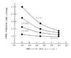
このレーザー光の照射時に試料を加熱することの意義について以下に説明する。図4に示すのは、ガラス基板上に下地の酸化珪素膜を形成し、その上に非晶質珪素膜を形成し、さらにその表面にニッケル元素を導入した非晶質珪素膜に対して、レーザー光を照射した際のラマンスペクトル強度を示したものである。そして各プロット点は、レーザー光を照射した際における試料の加熱温度を示す。
【0019】
図4におけるラマン強度は、単結晶珪素ウエハーのラマンスペクトルの強度I0 と試料に対するラマンスペクトル強度Iとの比率(I/I0 )で示される相対値である。ラマンスペクトルの強度は図7に示すようなラマンスペクトルの強度の最大値でもって定義される。一般に単結晶珪素ウエハーを越える結晶構造は存在しないので、図4の縦軸で示されるラマン強度の最大値は1である。このラマン強度の値が1に近い程、単結晶に近い構造を有するものと理解することができる。
【0020】
図5に示すのは、ラマンスペククトルの半値幅とレーザー光の照射エネルギー密度との関係を試料の加熱温度の違い毎にプロットしたものである。図5に示す縦軸の半値幅は、単結晶珪素ウエハーのラマンスペクトルの強度が半分の位置におけるスペクトルの幅W0 と実際に得られた試料のラマンスペクトルの強度が半分の位置におけるスペクトルの幅Wとの比(W/W0 )で示されるパラメータである。これらWやW0 は、図7に示すようなラマンスペクトルの強度が1/2の場所でのスペクトルの幅として定義される。一般にラマンスペクトルの幅が狭くシャープな程、その結晶性が優れていることを意味する。よって、一般的には単結晶珪素のラマンスペクトルの幅が最も狭くシャープなものとなる。なお試料は、図4に示すデータを得たものと同様のものを用いている。
【0021】
従って、図5に示す半値幅は、一般的には1以上の値となる。またその値が1に近い程、単結晶に近い構造を有していると理解することができる。図5を見れば明らかなように、レーザー光の照射時における試料の加熱温度を高くすることによって、単結晶に近い結晶性を得ることができる。またこの試料の加熱に従う効果は500℃程度で飽和することが理解される。図5から、安定して単結晶に近い結晶性を得るためには、400℃の加熱では確実ではなく、余裕をみて450℃以上とするのが好ましいことが結論される。
【0022】
本発明者等の知見によれば、図4に示すラマン強度が0.8 以上であり、また図5に示すラマンスペクトルの半値幅が2.0 以下であり、またその領域内に結晶粒界が実質的に存在していない場合、当該領域を単結晶と見なせる領域として見ることができる。
【0023】
この単結晶と見なせる領域は、プラズマCVD法や減圧熱CVD法でもって成膜された珪素膜を出発膜としており、膜中には、炭素と窒素とが1×10¹⁶〜5×1018cm-3、酸素が1×10¹⁷〜5×1019cm-3の濃度で含まれている。また原理的に格子欠陥が存在しているので、珪素の不対結合手を中和するために水素を1×10¹⁷〜5×1020cm-3の濃度で含んでいる。即ち、この単結晶と見なせる領域は、点欠陥を有してはいるが、線欠陥や面欠陥は有していないことが特徴である。なお、これら含有されている元素の濃度は、SIMS(2次イオン分析法)で計測される値の最低値として定義される。
【0024】
上記単結晶と見なせる領域は、一般的な単結晶ウエハーとは異なるものである。これは、CVD法で形成され、その厚さが200〜2000Å程度の薄膜半導体であることに起因する。
【0025】
他の発明の構成は、
絶縁表面を有する基板上に形成れた薄膜珪素半導体を用いた半導体装置であって、
前記薄膜珪素半導体は、実質的に単結晶と見なせる領域を有し、
前記領域は活性層の少なくも一部を構成しており、
前記領域中には、炭素及び窒素の原子が1×1016cm-3〜5×1018cm-3の濃度で、かつ酸素の原子が1×1017cm-3〜5×1019cm-3の濃度で含まれていることを特徴とする。
【0026】
他の発明の構成は、
絶縁表面を有する基板上に形成れた薄膜珪素半導体を用いた半導体装置であって、
前記薄膜珪素半導体は、実質的に単結晶と見なせる領域を有し、 前記領域は活性層の少なくも一部を構成しており、
前記領域中には、珪素の不対結合手を中和している水素の原子が1×1017cm-3〜5×1020cm-3の濃度で含まれていることを特徴とする半導体装置。
【0027】
他の発明の構成は、
絶縁表面を有する基板上に形成れた薄膜珪素半導体を用いた半導体装置であって、
前記薄膜珪素半導体は、実質的に単結晶と見なせる領域を有し、 前記領域は活性層の少なくも一部を構成しており、
前記領域中には、炭素及び窒素の原子が1×1016cm-3〜5×1018cm-3の濃度で、かつ酸素の原子が1×1017cm-3〜5×1019cm-3の濃度で、かつ珪素の不対結合手を中和している水素の原子が1×1017cm-3〜5×1020cm-3の濃度で含まれており、
前記薄膜珪素半導体の厚さは平均で200Å〜2000Åであることを特徴とする。
【0028】
他の発明の構成は、
絶縁表面を有する基板上に形成れた薄膜珪素半導体を用いた半導体装置であって、
前記薄膜珪素半導体の実質的に単結晶と見なせる結晶構造を有する領域が少なくともチャネル形成領域を構成しており、
前記チャネル形成領域中には、炭素及び窒素の原子が1×1016cm-3〜5×1018cm-3の濃度で、かつ酸素の原子が1×1017cm-3〜5×1019cm-3の濃度で、かつ珪素の不対結合手を中和している水素の原子が1×1017cm-3〜5×1020cm-3の濃度で含まれていることを特徴とする。
【0029】
他の発明の構成は、
絶縁表面を有する基板上に形成された珪素薄膜に対してレーザー光を照射し単結晶と見なせる領域を形成する工程を有し、
前記レーザー光の照射は、試料を450℃〜750℃の温度に加熱した状態で行われることを特徴とする。
【0030】
他の発明の構成は、
複数の薄膜トランジスタが並列に接続された構造を有し、
前記複数の薄膜トランジスタのそれぞれは少なくともチャネル形成領域中に実質的に結晶粒界が存在しない構造を有し、
ていることを特徴とする。
【0031】
他の発明の構成は、
複数の薄膜トランジスタが並列に接続された構造を有し、
前記複数の薄膜トランジスタのそれぞれは少なくともチャネル形成領域中に実質的に結晶粒界が存在しない構造を有し、
前記チャネル形成領域中には、炭素及び窒素の原子が1×1016cm-3〜5×1018cm-3の濃度で、かつ酸素の原子が1×1017cm-3〜5×1019cm-3の濃度で、かつ珪素の不対結合手を中和している水素の原子が1×1017cm-3〜5×1020cm-3の濃度で含まれていることを特徴とする。
【0032】
他の発明の構成は、
複数の薄膜トランジスタが並列に接続された構造を有し、
前記複数の薄膜トランジスタのそれぞれは少なくともチャネル形成領域中に実質的に結晶粒界が存在しない構造を有し、
前記チャネル形成領域は200Å〜2000Åの厚さを有し、
前記チャネル形成領域中には、炭素及び窒素の原子が1×1016cm-3〜5×1018cm-3の濃度で、かつ酸素の原子が1×1017cm-3〜5×1019cm-3の濃度で、かつ珪素の不対結合手を中和している水素の原子が1×1017cm-3〜5×1020cm-3の濃度で含まれていることを特徴とする。
【0033】
他の発明の構成は、
複数の薄膜トランジスタが並列に接続された構造を有し、
前記複数の薄膜トランジスタのそれぞれは少なくともチャネル形成領域が実質的に単結晶と見なせる薄膜珪素半導体で構成されていることを特徴とする。
【0034】
【作用】
薄膜珪素半導体の単結晶と見なせる領域を活性層として用いて薄膜トランジスタを構成することで、耐圧が高く、また特性の変動や劣化の無い薄膜トランジスタを得ることができる。
【0035】
また、薄膜珪素半導体の単結晶と見なせる領域を活性層として用いて構成した薄膜トランジスタを複数並列に接続した構成を採用することで、大電流を流すことのできる構成を得ることができる。このような構成は、実質的にチャネル幅を大きくするのと同様な効果を得ることができる。この構成を採用すると、単結晶と見なせる半導体で構成したトランジスタと等価の特性を得ることができ、高い移動度、大きな耐圧、安定した特性を得ることができる。
【0036】
【実施例】
〔実施例1〕
本実施例は、基板としてガラス基板(コーニング7059)を用い、このガラス基板の歪点温度以下の温度で、薄膜トランジスタを作製する例である。コーニング7059ガラス基板の歪点は、593℃であり、この温度以上の温度での加熱処理は、ガラス基板の縮や変形を招くことになり好ましくない。特に大型の液晶表示装置に利用するために大面積を有するガラス基板を用いた場合には、ガラス基板の縮や変形の影響が顕著になってしまう。
【0037】
そこで、本実施例で示す薄膜トランジスタは、加熱処理工程における最高温度を600℃以下、好ましくは550℃以下とすることによって、基板に対する熱の影響を大きく低減させることを特徴とする。
【0038】
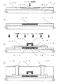
図1に本実施例で示す薄膜トランジスタの作製工程を示す。まず石英基板101上に下地膜として酸化珪素膜102を3000Åの厚さにスパッタ法によって形成する。次に非晶質珪素膜103を500Åの厚さにプラズマCVD法または減圧熱CVD法によって成膜する。(図1(A))
【0039】
非晶質珪素膜103を形成した後、600℃の温度で加熱処理を施し、非晶質珪素膜103を結晶化させる。そしてレーザー光を照射し、104で示される領域を中心として結晶成長を行わせ、単結晶と見なせる結晶領域106を得る。このレーザー光の照射は、試料または被照射面を600℃の温度に加熱しながら行う。このレーザー光の照射は、図1の104で示される領域に対して行われ、その際、104で示される領域から周辺へと結晶成長が進行していく。(図1(A))
【0040】
上記工程において、非晶質珪素膜に結晶化を助長する金属元素を導入することは有効である。こうすることによって、より大きな面積に渡って単結晶と見なせる領域を形成することができる。
【0041】
単結晶と見なせる領域106を得たら、この領域を用いて薄膜トランジスタの活性層をパターニングより形成する。活性層は、その全体が単結晶と見なせる領域内に形成されるのが最も好ましい。しかし、活性層の大きさによっては、得られる単結晶領域が相対的に小さく、活性層全体を構成することが困難な場合もある。この場合は、少なくともチャネル形成領域を単結晶と見なせる領域とすることで、チャネル形成領域内に結晶粒界が存在しない状態とすることができる。
【0042】
活性層を形成したら、ゲイト絶縁膜として酸化珪素膜107を1000Åの厚さにプラズマCVD法で成膜する。そして、スカンジウムが0.2 %含まれたアルミニウムを主成分とする膜を6000Åの厚さに成膜する。次にこのアルミニウムを主成分とする膜をパターニングすることにより、ゲイト電極108を得る。
【0043】
そして酒石酸を10%含んだエチレングルコール溶液中でゲイト電極108を陽極として陽極酸化を行うことで、酸化物層109を形成する。この酸化物層109の厚さは2000Å程度する。この酸化物層が存在することで、後の不純物イオン注入の工程において、オフセットゲイト領域を形成することができる。
【0044】
次にNチャネル型の薄膜トランジスタであればリンのイオンを、Pチャネル型の薄膜トランジスタであればボロンのイオンを不純物イオンとして活性層に注入する。この工程において、ゲイト電極108とその周囲の酸化物層109がマスクとなり、110と114で示される領域に不純物イオンが注入される。そして不純物イオンが注入された110の領域はソース領域に、また114の領域はドレイン領域として形成される。またゲイト電極108の周囲の酸化物層109がマスクとなり、オフセットゲイト領域111と113とが同時に形成される。またチャネル形成領域112も自己整合的に形成される。(図1(C))
【0045】
不純物イオンの注入工程の終了後、レーザー光を照射し、不純物イオンの注入によって損傷した活性層のアニールと注入された不純物の活性化を行う。この工程は、赤外光等の強光を照射することによって行ってもよい。
【0046】
さらに層間絶縁膜として酸化珪素膜115をプラズマCVD法で7000Åの厚さに成膜する。さらに穴開け工程を経て、ソース電極116とドレイン電極117を形成しする。さらに350℃の水素雰囲気中において加熱処理を行うことにより、薄膜トランジスタを完成させる。(図1(D))
【0047】
本実施例で示す薄膜トランジスタは、活性層が単結晶と見なせる構造を有した領域で構成されているので、結晶粒界に起因する耐圧の低さの問題やリーク電流が大きいという問題を解決することができる。
【0048】
〔実施例2〕
本実施例は、結晶化を助長する金属元素を非晶質珪素膜に導入することにより、単結晶と見なせる結晶領域を形成し、この結晶性を有する領域を用いて薄膜トランジスタを構成した例を示す。
【0049】
図2に本実施例の作製工程を示す。まずガラス基板101上に下地膜として酸化珪素膜102を3000Åの厚さにスパッタ法によって形成する。そして非晶質珪素膜103をプラズマCVD法または減圧熱CVD法で1000Åの厚さに成膜する。そして非晶質珪素膜の表面にUV酸化法によって、極薄い酸化膜(図示せず)を形成する。この酸化膜は後の溶液塗布工程において、溶液の濡れ性を良くするためのものである。ここで行うUV酸化工程は、酸化性雰囲気中においてUV光を照射することによって、被照射面の表面に極薄い酸化膜を形成するものである。
【0050】
次にニッケル酢酸塩溶液を極薄い酸化膜が形成された非晶質珪素膜103の表面にスピンコート法によってコーティングし、ニッケルを含有した被膜100を形成する。この被膜100が存在することで、極薄い酸化膜を介してニッケル元素が非晶質珪素膜に接して配置された状態となる。
【0051】
この状態で550℃、4時間の加熱処理を施し、非晶質珪素膜103を結晶性珪素膜に変成させる。ここでは、結晶化を助長する金属元素であるニッケルが導入されているので、550℃、4時間程度の加熱処理で結晶性珪素膜を得ることができる。
【0052】
加熱処理によって結晶性珪素膜に変成された珪素膜103を得たら、レーザー光を照射することによって、図2の104で示される領域から結晶成長を行わす。本実施例の場合は、結晶化を助長する金属元素であるニッケルが導入されているので、106で示されるような単結晶と見なせる領域を容易に得ることができる。
【0053】
こうして図2(B)に示されるような単結晶と見なせる領域106を得たら、その領域を利用して、薄膜トランジスタの活性層を形成する。また、ニッケルを含有した被膜は、活性層の形成前または形成後に取り除く。
【0054】
活性層を形成したら、ゲイト絶縁膜107を酸化珪素膜で構成し、さらにアルミニウムを主成分としたゲイト電極108とその周囲の酸化物層109を形成する。これらの作製工程は実施例1で示したものと同様である。
【0055】
こうして図2(C)に示す状態を得たら、不純物イオンの注入を行い、ソース領域110とドレイン領域114の形成を行う。この工程において、オフセットゲイト領域111と113、さらにチャネル形成領域112は自己整合的に形成される。
【0056】
さらにレーザー光の照射を行い、不純物イオンの注入時における損傷と注入されれた不純物イオンの活性化を行う。
【0057】
そして、層間絶縁膜として酸化珪素膜115をプラズマCVD法で形成し、穴開け工程を経て、ソース電極116とドレイン電極117を形成する。最後に350℃の水素雰囲気中において1時間の加熱処理を行うことで、図2(D)に示す薄膜トランジスタを完成させる。
【0058】
〔実施例3〕
本実施例は、大電流を扱う必要がある薄膜トランジスタに本明細書で開示する発明を利用した構成に関する。例えばアクティブマトリクス型の液晶表示装置の周辺回路には、数十万個以上配置された画素トランジスタを駆動するために、大電流を流すことのできるバッファーアンプ(出力インピーダンスの低い電力変換回路)が必要とされる。そして、1枚の基板上に表示領域のみならず、周辺回路領域をも一体化して集積化しようとする場合、このバッファーアンプをも薄膜トランジスタで構成する必要が生じる。
【0059】
このようなバッファーアンプに用いることのできる薄膜トランジスタを構成するには、薄膜トランジスタのチャネル形成領域の幅を数十μmあるいはそれ以上のものとする必要がある。しかし一般の多結晶または微結晶構造を有する結晶性珪素薄膜を用いた場合には、耐圧が低く、必要とするバッファーアンプを構成することが困難であるという問題がある。また高速動作を行わせる場合に、特性のバラツキやドリフトが生じやすいという問題がある。これは、各トランジスタにおいてしきい値が変動したり、特性に劣化が生じやすいことに起因すう。また、発熱の問題も大きく、発熱の影響で特性が劣化してしまうという問題もある。これらの問題は、活性層(特にチャネル形成領域)に結晶粒界が存在していることが主な原因である。
【0060】
そこで、本実施例においては、一つ一つが単結晶とみなせる領域を用いてチャネル形成領域を構成した薄膜トランジスタを複数個並列に接続し、等価的に大きなチャネル幅を有する薄膜トランジスタと同様の大電流を取り扱うことのできる構成を提供するものである。
【0061】
図3に本実施例に示す薄膜トランジスタの構成を示す。本実施例に示す構成においては、薄膜トランジスタを並列に3つ接続した構成を示す。図3に示す構成においては、それぞれの薄膜トランジスタのチャネル形成領域とその周辺部を構成する活性層を単結晶と見なせる珪素半導体薄膜で構成している。
【0062】
図3において、301で示す領域が単結晶と見なせる領域である。この106で示される単結晶とみなせる領域は、チャネル形成領域とソース/ドレイン領域の一部を含んでいる。従って、チャネル形成領域のみならず、ソース領域とチャネル形成領域との界面およびその近傍、ドレイン領域とチャネル形成領域との界面およびその近傍を単結晶と見なせる構造とすることができる。
【0063】
このような構成を採用した場合、結晶粒界の存在に起因する問題を解決することができる。即ち、耐圧の低さの問題、特性の劣化の問題、しきい値が変動してしまう問題を解決することができる。また、結晶粒界を経由してソース/ドレイン間を移動するキャリアを減少させることができるので、OFF電流を小さくすることができる。
【0064】
図3に示す構成をA−A’で切った断面は図1(D)に対応する。即ち、図3に示す構成は、図1(D)に示す薄膜トランジスタを3つ並列に接続した構成を有している。各トランジスタは共通のゲイト電極を有し、ソース電極とドレイン電極とは、コンタクト305と306とによって、共通に配線されている。
【0065】
本実施例に示す構成を採用した場合、1つ当たりの薄膜トランジスタのチャネル幅が20μmであっても、3個の薄膜トランジスタを並列に接続することにより、60μmのチャネル幅を有する薄膜トランジスタと等価の動作を行わすことができる。
【0066】
本実施例では、薄膜トランジスタを3つ並列に接続する例を示した。しかし、並列に接続する薄膜トランジスタの数は必要とする数を選ぶことができる。
【0067】
本実施例に示すような構成を採用することにより、単結晶と見なせる半導体を用いた薄膜トランジスタと同等の特性を有し、かつ大電流を扱うことのできる薄膜トランジスタを得ることができる。従って、高速動作を行わすこができ、しかも特性の劣化や変化のない構成を実現することができる。
【0068】
本実施例に示すような構成は、大電流を流す必要のある回路、例えばアクティブマトリクス型の液晶表示装置の周辺回路に配置されるバッファー回路に最適な構成といえる。
【0069】
〔実施例4〕
本明細書に開示する発明を用いて、より高度なアクティブマトリクス型液晶ディスプレーシステムを構築する例を図6に示す。図6の例は、一対の基板間に液晶を挟持した構成を有する液晶ディスプレーの少なくとも一方の基板上に、通常のコンピュータのメインボードに取り付けられている半導体チップを固定することによって、小型化、軽量化、薄型化をおこなった例である。
【0070】
以下、図6について説明する。基板15は液晶ディスプレーの基板でもあり、その上にはTFT11、画素電極12、補助容量13を具備する画素が多数形成されたアクティブマトリクス回路14と、それを駆動するためのXデコーダー/ドライバー、Yデコーダー/ドライバー、XY分岐回路がTFTによって形成されている。アクティブマトリクス回路を駆動するためには、低出力インピーダンスを有するバッファー回路を周辺回路に配置する必要があるが、このバッファー回路を図3に示すような回路を応用して構成することは有用である。
【0071】
そして基板15上に、さらに他のチップを取り付ける。そして、これらのチップはワイヤボンディング法、COG(チップ・オン・グラス)法等の手段によって、基板15上の回路に接続される。図6において、補正メモリー、メモリー、CPU、入力ポートは、このようにして取り付けられたチップであり、この他にも様々なチップを取り付けてもよい。
【0072】
図6において、入力ポートとは、外部から入力された信号を読み取り、画像用信号に変換する回路である。補正メモリーは、アクティブマトリクスパネルの特性に合わせて入力信号等を補正するためのパネルに固有のメモリーのことである。特に、この補正メモリーは、各画素固有の情報を不揮発性メモリーとして有し、個別に補正するためのものである。すなわち、電気光学装置の画素に点欠陥のある場合には、その点の周囲の画素にそれに合わせて補正した信号を送り、点欠陥をカバーし、欠陥を目立たなくする。または、画素が周囲の画素に比べて暗い場合には、その画素により大きな信号を送って、周囲の画素と同じ明るさとなるようにするものである。画素の欠陥情報はパネルごとに異なるので、補正メモリーに蓄積されている情報はパネルごとに異なる。
【0073】
CPUとメモリーは通常のコンピュータのものとその機能は同様で、特にメモリーは各画素に対応した画像メモリーをRAMとして持っている。これらのチップはいずれもCMOS型のものである。
【0074】
また必要とする集積回路の少なくとも一部を本明細書で開示する発明で構成し、システムの薄膜をさらに高めてもよい。
以上のように、液晶ディスプレー基板にCPU、メモリーまでもが形成され、1枚の基板で簡単なパーソナルコンピュータのような電子装置を構成することは、液晶表示システムを小型化し、その応用範囲を広げるために非常に有用である。
【0075】
本実施例に示すようにシステム化された液晶ディスプレーの必要とする回路に本明細書で開示する発明を用いて作製した薄膜トランジスタを利用することができる。特に、単結晶と見なせる領域を用いて作製された薄膜トランジスタをアナログバッファー回路やその他必要とする回路に利用することは極めて有用である。
【0076】
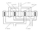
〔実施例5〕
本実施例は、図8に示すように3つの薄膜トランジスタを並列に接続した構成に関する。図8において、804で示されるが共通の活性層であり、803で示されるのが活性層中に形成されている単結晶と見なせる領域である。図8には、単結晶と見なせる3つの領域が示されており、この3つの単結晶と見なせる領域にそれぞれの薄膜トランジスタのチャネル形成領域が形成される。
【0077】
801は共通のゲイト電極およびゲイト配線である。805は共通のソース電極およびソース配線である。806は共通のドレイン電極およびドレイン配線である。そして802で示されるのが、ソース/ドレイン電極とソース/ドレイン領域とのコンタクト部分である。
【0078】
【発明の効果】
本明細書で開示する発明を利用することで、結晶粒界の影響を受けない薄膜トタンジスタを得ることができる。そして耐圧が高く、特性の変動がなく、さらに大電流を扱うことのできる薄膜トランジスタを得ることができる。また薄膜トランジスタの動作が結晶粒界の影響を受けないものとすることができるので、OFF電流の小さな特性とすることができる。
【図面の簡単な説明】
【図1】 実施例の薄膜トランジスタの作製工程を示す。
【図2】 実施例の薄膜トランジスタの作製工程を示す。
【図3】 実施例の薄膜トランジスタの構成を示す。
【図4】 試料の加熱温度を変化させた場合のレーザー光の照射エネルギー密度とラマン強度との関係を示す。
【図5】 試料の加熱温度を変化させた場合のレーザー光の照射エネルギー密度とラマンスペクトルの半値幅との関係を示す。
【図6】 1枚の基板上に集積化された液晶電気光学装置の例を示す。
【図7】 ラマンスペクトルの1例を示す。
【図8】 実施例の薄膜トランジスタの構成を示す。
【符号の説明】
101 ガラス基板
102 下地膜(酸化珪素膜)
103 珪素膜
104 レーザー光が照射される領域
105 非晶質珪素膜として残存する領域
106 単結晶と見なせる領域
107 ゲイト絶縁膜(酸化珪素膜)
108 ゲイト電極
109 陽極酸化物層
110 ソース領域
111、113 オフセットゲイト領域
114 ドレイン領域
115 層間絶縁膜
116 ソース電極
117 ドレイン電極
100 ニッケルを含有した膜
305、306 コンタクト領域[0001]
[Prior art]
In recent years, a technique for forming a transistor (referred to as a thin film transistor) using a thin film semiconductor over a glass or quartz substrate has been studied. In particular, a technique using amorphous silicon (amorphous silicon) as a thin film semiconductor has been put into practical use and is used in an active matrix liquid crystal display device and the like.
[0002]
However, a thin film transistor using amorphous silicon has a problem that its characteristics are low. For example, when a higher function is required as a display function of an active matrix liquid crystal display device, the characteristics of a thin film transistor using an amorphous silicon film are too low.
[0003]
A technique for forming a thin film transistor using a crystalline silicon film obtained by crystallizing an amorphous silicon film is also known. This technique transforms an amorphous silicon film into a crystalline silicon film by performing heat treatment or laser light irradiation after the formation of the amorphous silicon film. A crystalline silicon film obtained by crystallizing an amorphous silicon film generally has a polycrystalline structure or a microcrystalline structure.
[0004]
When a thin film transistor is formed using a crystalline silicon film, much higher characteristics can be obtained than when an amorphous silicon film is used. For example, when viewed in terms of mobility, which is one index for evaluating the characteristics of thin film transistors, the mobility of a thin film transistor using an amorphous silicon film is 1 cm. 2 / Vs or less, but for a thin film transistor using a crystalline silicon film, 100 cm 2 / Vs or so.
[0005]
However, the crystalline silicon film obtained by crystallizing the amorphous silicon film has a polycrystalline structure, and has a number of problems due to crystal grain boundaries. For example, there is a problem that the breakdown voltage of the thin film transistor is greatly limited because there are carriers that move via the crystal grain boundaries. In addition, there is a problem that characteristic changes and deterioration are likely to occur when performing high-speed operation. There is also a problem that leakage current (leakage current) is increased when the thin film transistor is OFF because there are carriers that move through the crystal grain boundary.
[0006]
In addition, when an active matrix liquid crystal display device is to be configured in a more integrated form, it is desired that not only the pixel region but also a peripheral circuit be formed on a single glass substrate. In such a case, in order to drive hundreds of thousands of pixel transistors arranged in a matrix, the thin film transistors arranged in the peripheral circuit are required to handle a large current.
[0007]
In order to obtain a thin film transistor capable of handling a large current, it is necessary to adopt a structure with a large channel width. However, a thin film transistor using a polycrystalline silicon thin film or a microcrystalline silicon thin film has a problem that even if the channel width is widened, it cannot be put into practical use due to the problem of breakdown voltage. There is also a problem that the fluctuation of the threshold value is large and is not practical.
[0008]
[Problems to be solved by the invention]
An object of the invention disclosed in this specification is to provide a thin film transistor which is not affected by a grain boundary.
Another object of the invention disclosed in this specification is to provide a thin film transistor which has a high withstand voltage and can handle a large current.
Another object of the invention disclosed in this specification is to provide a thin film transistor which has no deterioration or fluctuation in characteristics.
[0009]
[Means for Solving the Problems]
One of the inventions disclosed in this specification is:
A semiconductor device using a thin film silicon semiconductor formed on a substrate having an insulating surface,
The thin-film silicon semiconductor has a region that can be substantially regarded as a single crystal, and the region constitutes at least a part of an active layer,
In the region, carbon and nitrogen atoms are 1 × 10 16 cm -3 ~ 5x10 18 cm -3 Concentration of oxygen atoms is 1 × 10 17 cm -3 ~ 5x10 19 cm -3 Of hydrogen atoms neutralizing dangling bonds of silicon at a concentration of 1 × 10 17 cm -3 ~ 5x10 20 cm -3 It is characterized by being contained at a concentration of.
[0010]
In the above structure, a region that can be regarded as substantially a single crystal refers to a region of a thin film silicon semiconductor having a crystal structure that is recognized as being equivalent to the crystallinity of a single crystal silicon wafer. Specifically, compared with the Raman spectrum of single crystal silicon, the intensity ratio of the Raman spectrum is 0.8 or more, the ratio of the half-value width (relative value) of the Raman spectrum is 2 or less, and at the same time A region where no crystal grain boundary substantially exists is defined as a region which can be regarded as a single crystal.
[0011]
The region which can be regarded as substantially single crystal as described above can be obtained by heating or laser light irradiation using an amorphous silicon film as a starting film. In particular, by introducing a metal element that promotes the crystallinity of silicon, a region that can be regarded as a single crystal over a large area can be obtained relatively easily.
[0012]
As a metal element that promotes crystallization of silicon, one or more elements selected from Fe, Co, Ni, Ru, Rh, Pd, Os, Ir, Pt, Cu, Zn, Ag, and Au are used. Can do. These elements have an intrusion type property with respect to silicon, and are diffused into the silicon film by heat treatment or laser light irradiation. Among these elements, Ni (nickel) is an element that can obtain a particularly remarkable effect.
[0013]
The concentration of the metal element is 1 × 10 3 in the final silicon film after crystallization is completed. 16 ~ 5x10 19 cm -3 It is important that it be included at a concentration of. The concentration of this metal element is 1 × 10 16 cm -3 If it is below, the effect of promoting crystallization cannot be obtained, and the concentration is 5 × 10 5. 19 cm -3 If it is as described above, the properties as a semiconductor are impaired.
[0014]
In order to form the above-mentioned region that can be regarded as a single crystal in the silicon thin film, there is a method as described below. First, an amorphous silicon film is formed on a glass substrate or a quartz substrate, and then a film containing nickel is formed on the surface of the amorphous silicon film. The nickel-containing film may be formed by forming a very thin nickel thin film by sputtering or the like, or by applying a nickel-containing solution on the surface of the amorphous silicon film, the nickel element is converted into amorphous silicon. A method of placing the film in contact with the surface of the film may be employed.
[0015]
When nickel element is introduced into the amorphous silicon film, the amorphous silicon film is crystallized by heat treatment. This heat treatment can be performed at a temperature of 600 ° C. or lower by the action of nickel element. When a glass substrate is used as the substrate, the temperature of this heat treatment is preferably as low as possible, but considering the efficiency of the crystallization step, it is performed at a temperature of 500 ° C. or higher, preferably 550 ° C. or higher. It is useful. When a quartz substrate is used as the substrate, this heat treatment can be performed at a temperature of 800 ° C. or higher, and a crystalline silicon film can be obtained in a single time. The crystalline silicon film obtained in this step has a polycrystalline or microcrystalline state, and crystal grain boundaries exist in the film.
[0016]
Therefore, the crystallinity is locally promoted by irradiating the sample with laser light at a temperature of 450 ° C. or higher. By this step, a region that can be regarded as a single crystal can be formed. It is important to heat the sample or the irradiated surface at a temperature of 450 ° C. or higher when performing this laser light irradiation. This heating temperature is preferably 450 ° C. to 750 ° C., particularly 450 ° C. to 600 ° C. when a glass substrate is used as the substrate.
[0017]
As another method for forming a region that can be regarded as a single crystal, an amorphous silicon film is formed and a metal element that promotes crystallization is introduced. And a method for forming a region that can be regarded as a region. Also in this case, it is important to heat the sample at a temperature of 450 ° C. to 750 ° C., particularly when a glass substrate is used as the substrate at the time of laser light irradiation.
[0018]
The significance of heating the sample during the laser light irradiation will be described below. FIG. 4 shows that an underlying silicon oxide film is formed on a glass substrate, an amorphous silicon film is formed thereon, and a nickel element is further introduced into the surface of the amorphous silicon film. The Raman spectrum intensity when irradiated with laser light is shown. Each plot point indicates the heating temperature of the sample when irradiated with laser light.
[0019]
The Raman intensity in FIG. 4 is the intensity I of the Raman spectrum of the single crystal silicon wafer. 0 And the ratio of the Raman spectral intensity I to the sample (I / I 0 ) Is a relative value. The intensity of the Raman spectrum is defined by the maximum value of the intensity of the Raman spectrum as shown in FIG. Since there is generally no crystal structure exceeding the single crystal silicon wafer, the maximum value of the Raman intensity indicated by the vertical axis in FIG. It can be understood that the closer the Raman intensity value is to 1, the closer the structure is to a single crystal.
[0020]
FIG. 5 shows a plot of the relationship between the half-value width of the Raman spectrum and the irradiation energy density of the laser beam for each difference in the heating temperature of the sample. The half width of the vertical axis shown in FIG. 5 is the width W of the spectrum at the position where the intensity of the Raman spectrum of the single crystal silicon wafer is half. 0 And the ratio of the spectrum width W at the position where the intensity of the Raman spectrum of the actually obtained sample is half (W / W 0 ). These W and W 0 Is defined as the width of the spectrum where the Raman spectrum intensity is ½ as shown in FIG. In general, the narrower and sharper the Raman spectrum, the better the crystallinity. Therefore, generally, the width of the Raman spectrum of single crystal silicon is the narrowest and sharpest. The sample used is the same as that obtained from the data shown in FIG.
[0021]
Therefore, the full width at half maximum shown in FIG. 5 is generally a value of 1 or more. It can be understood that the closer the value is to 1, the closer the structure is to a single crystal. As is apparent from FIG. 5, crystallinity close to that of a single crystal can be obtained by increasing the heating temperature of the sample at the time of laser light irradiation. It is understood that the effect of heating the sample is saturated at about 500 ° C. From FIG. 5, it is concluded that heating at 400 ° C. is not reliable in order to obtain crystallinity close to a single crystal stably, and it is preferable to set the temperature to 450 ° C. or more with a margin.
[0022]
According to the knowledge of the present inventors, the Raman intensity shown in FIG. 4 is 0.8 or more, the half width of the Raman spectrum shown in FIG. 5 is 2.0 or less, and the grain boundary is substantially within the region. When it does not exist, the region can be viewed as a region that can be regarded as a single crystal.
[0023]
The region that can be regarded as a single crystal starts from a silicon film formed by plasma CVD or low-pressure thermal CVD, and carbon and nitrogen are contained in the film at 1 × 10 5. 16 ~ 5x10 18 cm -3 , Oxygen is 1 × 10 17 ~ 5x10 19 cm -3 Contained at a concentration of In addition, since lattice defects exist in principle, 1 × 10 hydrogen is used to neutralize dangling bonds of silicon. 17 ~ 5x10 20 cm -3 Contains at a concentration of That is, the region that can be regarded as a single crystal has a point defect but does not have a line defect or a plane defect. The concentration of these contained elements is defined as the lowest value measured by SIMS (secondary ion analysis).
[0024]
The region which can be regarded as the single crystal is different from a general single crystal wafer. This is because the thin film semiconductor is formed by CVD and has a thickness of about 200 to 2000 mm.
[0025]
Other aspects of the invention are:
A semiconductor device using a thin film silicon semiconductor formed on a substrate having an insulating surface,
The thin film silicon semiconductor has a region that can be substantially regarded as a single crystal,
The region comprises at least part of the active layer;
In the region, carbon and nitrogen atoms are 1 × 10 16 cm -3 ~ 5x10 18 cm -3 Concentration of oxygen atoms is 1 × 10 17 cm -3 ~ 5x10 19 cm -3 It is characterized by being contained at a concentration of.
[0026]
Other aspects of the invention are:
A semiconductor device using a thin film silicon semiconductor formed on a substrate having an insulating surface,
The thin-film silicon semiconductor has a region that can be substantially regarded as a single crystal, and the region constitutes at least a part of an active layer,
In the region, there are 1 × 10 5 hydrogen atoms neutralizing dangling bonds of silicon. 17 cm -3 ~ 5x10 20 cm -3 A semiconductor device characterized by being contained at a concentration of
[0027]
Other aspects of the invention are:
A semiconductor device using a thin film silicon semiconductor formed on a substrate having an insulating surface,
The thin-film silicon semiconductor has a region that can be substantially regarded as a single crystal, and the region constitutes at least a part of an active layer,
In the region, carbon and nitrogen atoms are 1 × 10 16 cm -3 ~ 5x10 18 cm -3 Concentration of oxygen atoms is 1 × 10 17 cm -3 ~ 5x10 19 cm -3 Of hydrogen atoms neutralizing dangling bonds of silicon at a concentration of 1 × 10 17 cm -3 ~ 5x10 20 cm -3 Is contained at a concentration of
The thin film silicon semiconductor has an average thickness of 200 to 2000 mm.
[0028]
Other aspects of the invention are:
A semiconductor device using a thin film silicon semiconductor formed on a substrate having an insulating surface,
A region having a crystal structure that can be regarded as a substantially single crystal of the thin film silicon semiconductor constitutes at least a channel formation region,
In the channel formation region, carbon and nitrogen atoms are 1 × 10 5. 16 cm -3 ~ 5x10 18 cm -3 Concentration of oxygen atoms is 1 × 10 17 cm -3 ~ 5x10 19 cm -3 Of hydrogen atoms neutralizing dangling bonds of silicon at a concentration of 1 × 10 17 cm -3 ~ 5x10 20 cm -3 It is characterized by being contained at a concentration of.
[0029]
Other aspects of the invention are:
A step of irradiating a silicon thin film formed on a substrate having an insulating surface with a laser beam to form a region that can be regarded as a single crystal;
The laser beam irradiation is performed in a state where the sample is heated to a temperature of 450 ° C. to 750 ° C.
[0030]
Other aspects of the invention are:
A plurality of thin film transistors connected in parallel;
Each of the plurality of thin film transistors has a structure in which at least a crystal grain boundary does not exist in a channel formation region,
It is characterized by.
[0031]
Other aspects of the invention are:
A plurality of thin film transistors connected in parallel;
Each of the plurality of thin film transistors has a structure in which at least a crystal grain boundary does not exist in a channel formation region,
In the channel formation region, carbon and nitrogen atoms are 1 × 10 5. 16 cm -3 ~ 5x10 18 cm -3 Concentration of oxygen atoms is 1 × 10 17 cm -3 ~ 5x10 19 cm -3 Of hydrogen atoms neutralizing dangling bonds of silicon at a concentration of 1 × 10 17 cm -3 ~ 5x10 20 cm -3 It is characterized by being contained at a concentration of.
[0032]
Other aspects of the invention are:
A plurality of thin film transistors connected in parallel;
Each of the plurality of thin film transistors has a structure in which at least a crystal grain boundary does not exist in a channel formation region,
The channel forming region has a thickness of 200 to 2000 mm,
In the channel formation region, carbon and nitrogen atoms are 1 × 10 5. 16 cm -3 ~ 5x10 18 cm -3 Concentration of oxygen atoms is 1 × 10 17 cm -3 ~ 5x10 19 cm -3 Of hydrogen atoms neutralizing dangling bonds of silicon at a concentration of 1 × 10 17 cm -3 ~ 5x10 20 cm -3 It is characterized by being contained at a concentration of.
[0033]
Other aspects of the invention are:
A plurality of thin film transistors connected in parallel;
Each of the plurality of thin film transistors is formed of a thin film silicon semiconductor in which at least a channel formation region can be substantially regarded as a single crystal.
[0034]
[Action]
By forming a thin film transistor by using a region that can be regarded as a single crystal of a thin film silicon semiconductor as an active layer, a thin film transistor with high withstand voltage and having no characteristic variation or deterioration can be obtained.
[0035]
In addition, by adopting a configuration in which a plurality of thin film transistors each configured by using a region that can be regarded as a single crystal of a thin film silicon semiconductor as an active layer are connected in parallel, a configuration capable of flowing a large current can be obtained. Such a configuration can achieve the same effect as substantially increasing the channel width. When this structure is employed, characteristics equivalent to those of a transistor formed using a semiconductor that can be regarded as a single crystal can be obtained, and high mobility, large breakdown voltage, and stable characteristics can be obtained.
[0036]
【Example】
[Example 1]
In this example, a glass substrate (Corning 7059) is used as a substrate, and a thin film transistor is manufactured at a temperature lower than the strain point temperature of the glass substrate. The strain point of Corning 7059 glass substrate is 593 ° C., and heat treatment at a temperature higher than this temperature is not preferable because it causes shrinkage or deformation of the glass substrate. In particular, when a glass substrate having a large area is used for use in a large liquid crystal display device, the influence of shrinkage or deformation of the glass substrate becomes significant.
[0037]
Therefore, the thin film transistor described in this embodiment is characterized in that the influence of heat on the substrate is greatly reduced by setting the maximum temperature in the heat treatment step to 600 ° C. or lower, preferably 550 ° C. or lower.
[0038]
FIG. 1 shows a manufacturing process of the thin film transistor shown in this embodiment. First, a
[0039]
After the
[0040]
In the above process, it is effective to introduce a metal element that promotes crystallization into the amorphous silicon film. In this way, a region that can be regarded as a single crystal over a larger area can be formed.
[0041]
When a
[0042]
After forming the active layer, a
[0043]
Then, an
[0044]
Next, phosphorus ions are implanted into the active layer as impurity ions for N-channel type thin film transistors and boron ions are implanted as impurity ions for P-channel type thin film transistors. In this step, the gate electrode 108 and the surrounding
[0045]
After completion of the impurity ion implantation step, laser light is irradiated to anneal the active layer damaged by the impurity ion implantation and activate the implanted impurities. This step may be performed by irradiating strong light such as infrared light.
[0046]
Further, a
[0047]
The thin film transistor shown in this embodiment is formed of a region having a structure in which the active layer can be regarded as a single crystal. Therefore, the problem of low breakdown voltage due to crystal grain boundaries and a problem of large leakage current are solved. Can do.
[0048]
[Example 2]
This embodiment shows an example in which a crystalline region that can be regarded as a single crystal is formed by introducing a metal element that promotes crystallization into an amorphous silicon film, and a thin film transistor is configured using the crystalline region. .
[0049]
FIG. 2 shows a manufacturing process of this embodiment. First, a
[0050]
Next, a nickel acetate solution is coated on the surface of the
[0051]
In this state, a heat treatment is performed at 550 ° C. for 4 hours to transform the
[0052]
When the
[0053]
When a
[0054]
After the formation of the active layer, the
[0055]
When the state shown in FIG. 2C is thus obtained, impurity ions are implanted, and the source region 110 and the drain region 114 are formed. In this step, the offset gate regions 111 and 113 and the channel formation region 112 are formed in a self-aligned manner.
[0056]
Further, laser light irradiation is performed to activate damage of the impurity ions and the implanted impurity ions.
[0057]
Then, a
[0058]
Example 3
This embodiment relates to a structure using the invention disclosed in this specification for a thin film transistor which needs to handle a large current. For example, the peripheral circuit of an active matrix liquid crystal display device requires a buffer amplifier (power conversion circuit with low output impedance) that can pass a large current to drive hundreds of thousands of pixel transistors. It is said. When it is intended to integrate not only the display area but also the peripheral circuit area on a single substrate, this buffer amplifier also needs to be formed of a thin film transistor.
[0059]
In order to form a thin film transistor that can be used in such a buffer amplifier, the width of the channel formation region of the thin film transistor needs to be several tens of μm or more. However, when a crystalline silicon thin film having a general polycrystalline or microcrystalline structure is used, there is a problem that the withstand voltage is low and it is difficult to construct a necessary buffer amplifier. In addition, when high-speed operation is performed, there is a problem that characteristic variation and drift are likely to occur. This is because the threshold value fluctuates in each transistor and the characteristics are likely to deteriorate. There is also a problem of heat generation, and there is also a problem that characteristics deteriorate due to the effect of heat generation. These problems are mainly caused by the presence of crystal grain boundaries in the active layer (particularly the channel formation region).
[0060]
Therefore, in this embodiment, a plurality of thin film transistors each of which forms a channel formation region are connected in parallel using a region that can be regarded as a single crystal, and a large current equivalent to that of a thin film transistor having an equivalently large channel width is obtained. A configuration that can be handled is provided.
[0061]
FIG. 3 shows a structure of the thin film transistor shown in this embodiment. In the structure shown in this embodiment, a structure in which three thin film transistors are connected in parallel is shown. In the configuration shown in FIG. 3, the channel formation region of each thin film transistor and the active layer that forms the periphery thereof are formed of a silicon semiconductor thin film that can be regarded as a single crystal.
[0062]
In FIG. 3, a region 301 is a region that can be regarded as a single crystal. A region which can be regarded as a single crystal indicated by 106 includes a channel formation region and a part of the source / drain region. Accordingly, not only the channel formation region but also the interface between the source region and the channel formation region and the vicinity thereof, and the interface between the drain region and the channel formation region and the vicinity thereof can be regarded as a single crystal.
[0063]
When such a configuration is adopted, problems caused by the presence of crystal grain boundaries can be solved. That is, it is possible to solve the problem of low withstand voltage, the problem of deterioration of characteristics, and the problem that the threshold value fluctuates. In addition, since carriers moving between the source / drain via the crystal grain boundary can be reduced, the OFF current can be reduced.
[0064]
A cross section taken along line AA ′ of the configuration shown in FIG. 3 corresponds to FIG. That is, the structure shown in FIG. 3 has a structure in which three thin film transistors shown in FIG. 1D are connected in parallel. Each transistor has a common gate electrode, and the source electrode and the drain electrode are wired in common by
[0065]
When the configuration shown in this embodiment is adopted, even if the channel width of each thin film transistor is 20 μm, an operation equivalent to that of a thin film transistor having a channel width of 60 μm is obtained by connecting three thin film transistors in parallel. Can be done.
[0066]
In this embodiment, an example in which three thin film transistors are connected in parallel is shown. However, the required number of thin film transistors connected in parallel can be selected.
[0067]
By adopting the structure shown in this embodiment, a thin film transistor having characteristics equivalent to those of a thin film transistor using a semiconductor that can be regarded as a single crystal and capable of handling a large current can be obtained. Therefore, a high-speed operation can be performed, and a configuration without deterioration or change in characteristics can be realized.
[0068]
The configuration shown in this embodiment can be said to be optimal for a circuit that needs to pass a large current, for example, a buffer circuit arranged in a peripheral circuit of an active matrix liquid crystal display device.
[0069]
Example 4
An example of constructing a more advanced active matrix type liquid crystal display system using the invention disclosed in this specification is shown in FIG. The example of FIG. 6 is miniaturized by fixing a semiconductor chip attached to a main board of a normal computer on at least one substrate of a liquid crystal display having a configuration in which a liquid crystal is sandwiched between a pair of substrates. This is an example of reducing the weight and thickness.
[0070]
Hereinafter, FIG. 6 will be described. The
[0071]
Then, another chip is attached on the
[0072]
In FIG. 6, an input port is a circuit that reads an externally input signal and converts it into an image signal. The correction memory is a memory unique to the panel for correcting an input signal or the like in accordance with the characteristics of the active matrix panel. In particular, this correction memory has information specific to each pixel as a non-volatile memory, and is used for individual correction. That is, if a pixel of the electro-optical device has a point defect, a signal corrected accordingly is sent to the pixels around the point to cover the point defect and make the defect inconspicuous. Alternatively, when the pixel is darker than the surrounding pixels, a larger signal is sent to the pixel so that the brightness is the same as that of the surrounding pixels. Since the pixel defect information varies from panel to panel, the information stored in the correction memory varies from panel to panel.
[0073]
The CPU and the memory have the same functions as those of a normal computer. In particular, the memory has an image memory corresponding to each pixel as a RAM. These chips are all of the CMOS type.
[0074]
Further, at least a part of the required integrated circuit may be constituted by the invention disclosed in this specification to further increase the thin film of the system.
As described above, even a CPU and a memory are formed on a liquid crystal display substrate, and configuring a simple electronic device such as a personal computer with a single substrate reduces the size of the liquid crystal display system and widens its application range. Is very useful for.
[0075]
As shown in this embodiment, a thin film transistor manufactured using the invention disclosed in this specification can be used for a circuit required for a systemized liquid crystal display. In particular, it is extremely useful to use a thin film transistor manufactured using a region that can be regarded as a single crystal for an analog buffer circuit and other necessary circuits.
[0076]
Example 5
This embodiment relates to a configuration in which three thin film transistors are connected in parallel as shown in FIG. In FIG. 8, a common active layer is indicated by 804, and a region indicated by 803 is a region that can be regarded as a single crystal formed in the active layer. FIG. 8 shows three regions that can be regarded as single crystals, and channel forming regions of the respective thin film transistors are formed in the regions that can be regarded as three single crystals.
[0077]
Reference numeral 801 denotes a common gate electrode and gate wiring.
[0078]
【The invention's effect】
By utilizing the invention disclosed in this specification, a thin-film transistor that is not affected by grain boundaries can be obtained. In addition, a thin film transistor that has a high breakdown voltage, does not vary in characteristics, and can handle a large current can be obtained. In addition, since the operation of the thin film transistor can be made free from the influence of crystal grain boundaries, the characteristics of a small OFF current can be obtained.
[Brief description of the drawings]
FIG. 1 shows a manufacturing process of a thin film transistor of an example.
FIG. 2 shows a manufacturing process of a thin film transistor of an example.
FIG. 3 shows a structure of a thin film transistor of an example.
FIG. 4 shows the relationship between the laser beam irradiation energy density and the Raman intensity when the heating temperature of the sample is changed.
FIG. 5 shows the relationship between the irradiation energy density of laser light and the half width of the Raman spectrum when the heating temperature of the sample is changed.
FIG. 6 shows an example of a liquid crystal electro-optical device integrated on a single substrate.
FIG. 7 shows an example of a Raman spectrum.
FIG. 8 shows a structure of a thin film transistor of an example.
[Explanation of symbols]
101 glass substrate
102 Base film (silicon oxide film)
103 Silicon film
104 Area irradiated with laser light
105 region remaining as an amorphous silicon film
106 Region that can be regarded as a single crystal
107 Gate insulating film (silicon oxide film)
108 Gate electrode
109 Anodic oxide layer
110 Source region
111, 113 Offset gate area
114 Drain region
115 Interlayer insulation film
116 Source electrode
117 Drain electrode
100 Film containing nickel
305, 306 Contact area
Claims (19)
前記基板上に配置された複数の画素と、
前記基板上に形成され、複数の薄膜トランジスタを用いて構成されたバッファー回路を含み、前記複数の画素を駆動する駆動回路と、
前記複数の薄膜トランジスタに共通のゲイト電極と、
前記複数の薄膜トランジスタのソース領域に接続された共通のソース電極と、
前記複数の薄膜トランジスタのドレイン領域に接続された共通のドレイン電極と、
を有し、
前記複数の薄膜トランジスタは、前記共通のゲイト電極、前記共通のソース電極及び前記共通のドレイン電極によって並列に接続されており、
前記複数の薄膜トランジスタのチャネル形成領域は、単結晶シリコンウェーハのラマンスペクトルに比較して、ラマンスペクトルの半値幅の比が2以下である珪素膜からなり、
前記珪素膜には、Niが含まれており、
前記複数の薄膜トランジスタのチャネル形成領域は分離して形成され、当該分離して形成されたチャネル形成領域はチャネル幅方向にならんで配置されていることを特徴とするアクティブマトリクス型の表示装置。A substrate having an insulating surface;
A plurality of pixels disposed on the substrate;
A drive circuit that is formed on the substrate and includes a buffer circuit configured using a plurality of thin film transistors, and that drives the plurality of pixels;
A gate electrode common to the plurality of thin film transistors;
A common source electrode connected to a source region of the plurality of thin film transistors;
A common drain electrode connected to drain regions of the plurality of thin film transistors;
Have
The plurality of thin film transistors are connected in parallel by the common gate electrode, the common source electrode, and the common drain electrode,
The channel formation region of the plurality of thin film transistors is composed of a silicon film in which the ratio of the half width of the Raman spectrum is 2 or less compared to the Raman spectrum of the single crystal silicon wafer,
The silicon film contains Ni,
An active matrix display device, wherein channel formation regions of the plurality of thin film transistors are formed separately, and the channel formation regions formed separately are arranged along a channel width direction.
前記基板上に配置された複数の画素と、
前記基板上に形成され、少なくとも第1の半導体薄膜を有する第1の薄膜トランジスタ及び第2の半導体薄膜を有する第2の薄膜トランジスタを用いて構成されたバッファー回路を含み、前記複数の画素を駆動する駆動回路と、
前記第1の薄膜トランジスタ及び前記第2の薄膜トランジスタに共通のゲイト電極と、
前記第1の半導体薄膜及び前記第2の半導体薄膜に接続された共通のソース電極と、
前記第1の半導体薄膜及び前記第2の半導体薄膜に接続された共通のドレイン電極と、
を有し、
前記第1の薄膜トランジスタ及び前記第2の薄膜トランジスタは、前記共通のゲイト電極、前記共通のソース電極及び前記共通のドレイン電極によって並列に接続されており、
前記第1の半導体薄膜及び前記第2の半導体薄膜は、単結晶シリコンウェーハのラマンスペクトルに比較して、ラマンスペクトルの半値幅の比が2以下である珪素膜からなり、
前記珪素膜には、Niが含まれており、
前記第1の半導体薄膜及び前記第2の半導体薄膜は分離して形成され、前記第1の半導体薄膜及び前記第2の半導体薄膜はチャネル幅方向にならんで配置されていることを特徴とするアクティブマトリクス型の表示装置。A substrate having an insulating surface;
A plurality of pixels disposed on the substrate;
A drive for driving the plurality of pixels, including a buffer circuit formed on the substrate and configured by using a first thin film transistor having at least a first semiconductor thin film and a second thin film transistor having a second semiconductor thin film. Circuit,
A gate electrode common to the first thin film transistor and the second thin film transistor;
A common source electrode connected to the first semiconductor thin film and the second semiconductor thin film;
A common drain electrode connected to the first semiconductor thin film and the second semiconductor thin film;
Have
The first thin film transistor and the second thin film transistor are connected in parallel by the common gate electrode, the common source electrode, and the common drain electrode,
The first semiconductor thin film and the second semiconductor thin film are made of a silicon film having a half-width ratio of Raman spectrum of 2 or less compared to the Raman spectrum of a single crystal silicon wafer,
The silicon film contains Ni,
The first semiconductor thin film and the second semiconductor thin film are formed separately, and the first semiconductor thin film and the second semiconductor thin film are arranged along the channel width direction. Matrix type display device.
前記基板上に配置された複数の画素と、
前記基板上に形成され、少なくとも第1の半導体薄膜を有する第1の薄膜トランジスタ及び第2の半導体薄膜を有する第2の薄膜トランジスタを用いて構成されたバッファー回路を含み、前記複数の画素を駆動する駆動回路と、
前記第1の薄膜トランジスタ及び前記第2の薄膜トランジスタに共通のゲイト電極と、
前記第1の半導体薄膜及び前記第2の半導体薄膜に接続された共通のソース電極と、
前記第1の半導体薄膜及び前記第2の半導体薄膜に接続された共通のドレイン電極と、
を有し、
前記第1の薄膜トランジスタ及び前記第2の薄膜トランジスタは、前記共通のゲイト電極、前記共通のソース電極及び前記共通のドレイン電極によって並列に接続されており、
前記第1の半導体薄膜及び前記第2の半導体薄膜は、単結晶シリコンウェーハのラマンスペクトルに比較して、ラマンスペクトルの半値幅の比が2以下である珪素膜からなり、
前記珪素膜には、Niが含まれており、
前記第1の半導体薄膜及び前記第2の半導体薄膜は直接互いに接していなく、前記第1の半導体薄膜及び前記第2の半導体薄膜はチャネル幅方向にならんで配置されていることを特徴とするアクティブマトリクス型の表示装置。A substrate having an insulating surface;
A plurality of pixels disposed on the substrate;
A drive for driving the plurality of pixels, including a buffer circuit formed on the substrate and configured by using a first thin film transistor having at least a first semiconductor thin film and a second thin film transistor having a second semiconductor thin film. Circuit,
A gate electrode common to the first thin film transistor and the second thin film transistor;
A common source electrode connected to the first semiconductor thin film and the second semiconductor thin film;
A common drain electrode connected to the first semiconductor thin film and the second semiconductor thin film;
Have
The first thin film transistor and the second thin film transistor are connected in parallel by the common gate electrode, the common source electrode, and the common drain electrode,
The first semiconductor thin film and the second semiconductor thin film are made of a silicon film having a half-width ratio of Raman spectrum of 2 or less compared to the Raman spectrum of a single crystal silicon wafer,
The silicon film contains Ni,
The first semiconductor thin film and the second semiconductor thin film are not in direct contact with each other, and the first semiconductor thin film and the second semiconductor thin film are arranged along the channel width direction. Matrix type display device.
Priority Applications (14)
| Application Number | Priority Date | Filing Date | Title |
|---|---|---|---|
| JP21807794A JP3897826B2 (en) | 1994-08-19 | 1994-08-19 | Active matrix display device |
| US08/513,090 US5731613A (en) | 1994-08-19 | 1995-08-09 | Semiconductor device having a monocrystalline layer composed of carbon, oxygen, hydrogen and nitrogen atoms |
| TW084108300A TW271012B (en) | 1994-08-19 | 1995-08-09 | |
| CNB001339990A CN100334743C (en) | 1994-08-19 | 1995-08-18 | Semiconductor device and its manufacture |
| CNB021278636A CN1194378C (en) | 1994-08-19 | 1995-08-18 | Active matrix display equipment |
| CN95109812A CN1091953C (en) | 1994-08-19 | 1995-08-18 | Semiconductor device and fabrication method thereof |
| CN2005100229952A CN1815743B (en) | 1994-08-19 | 1995-08-18 | Semiconductor device and method of fabricating the same |
| CNB2004100694517A CN100420026C (en) | 1994-08-19 | 1995-08-18 | Semiconductor device and method of fabrication thereof |
| KR19950025822A KR960009230A (en) | 1994-08-19 | 1995-08-19 | |
| US08/938,310 US5959313A (en) | 1994-08-19 | 1997-09-26 | Thin film semiconductor having a monocrystalline region containing carbon, nitrogen and oxygen and crystallization promotor metal component |
| KR1020010034585A KR100429943B1 (en) | 1994-08-19 | 2001-06-19 | Active matrix type display device |
| US10/926,006 US7557377B2 (en) | 1994-08-19 | 2004-08-26 | Semiconductor device having thin film transistor |
| US11/396,718 US7550765B2 (en) | 1994-08-19 | 2006-04-04 | Semiconductor device and fabrication method thereof |
| US12/492,498 US8450743B2 (en) | 1994-08-19 | 2009-06-26 | Semiconductor device having parallel thin film transistors |
Applications Claiming Priority (1)
| Application Number | Priority Date | Filing Date | Title |
|---|---|---|---|
| JP21807794A JP3897826B2 (en) | 1994-08-19 | 1994-08-19 | Active matrix display device |
Related Child Applications (1)
| Application Number | Title | Priority Date | Filing Date |
|---|---|---|---|
| JP2006132308A Division JP4481271B2 (en) | 2006-05-11 | 2006-05-11 | Display device |
Publications (2)
| Publication Number | Publication Date |
|---|---|
| JPH0864834A JPH0864834A (en) | 1996-03-08 |
| JP3897826B2 true JP3897826B2 (en) | 2007-03-28 |
Family
ID=16714284
Family Applications (1)
| Application Number | Title | Priority Date | Filing Date |
|---|---|---|---|
| JP21807794A Expired - Fee Related JP3897826B2 (en) | 1994-08-19 | 1994-08-19 | Active matrix display device |
Country Status (5)
| Country | Link |
|---|---|
| US (5) | US5731613A (en) |
| JP (1) | JP3897826B2 (en) |
| KR (2) | KR960009230A (en) |
| CN (5) | CN1815743B (en) |
| TW (1) | TW271012B (en) |
Families Citing this family (64)
| Publication number | Priority date | Publication date | Assignee | Title |
|---|---|---|---|---|
| US6008078A (en) * | 1990-07-24 | 1999-12-28 | Semiconductor Energy Laboratory Co., Ltd. | Method for manufacturing a semiconductor device |
| JP3562588B2 (en) * | 1993-02-15 | 2004-09-08 | 株式会社半導体エネルギー研究所 | Method for manufacturing semiconductor device |
| US6867432B1 (en) * | 1994-06-09 | 2005-03-15 | Semiconductor Energy Lab | Semiconductor device having SiOxNy gate insulating film |
| JP3897826B2 (en) * | 1994-08-19 | 2007-03-28 | 株式会社半導体エネルギー研究所 | Active matrix display device |
| JP3442500B2 (en) | 1994-08-31 | 2003-09-02 | 株式会社半導体エネルギー研究所 | Method for manufacturing semiconductor circuit |
| US6670640B1 (en) | 1994-09-15 | 2003-12-30 | Semiconductor Energy Laboratory Co., Ltd. | Method for producing semiconductor device |
| US6331475B1 (en) | 1995-01-12 | 2001-12-18 | Semiconductor Energy Laboratory Co., Ltd. | Method and manufacturing semiconductor device |
| US7271410B2 (en) * | 1995-03-28 | 2007-09-18 | Semiconductor Energy Laboratory Co., Ltd. | Active matrix circuit |
| JPH08264802A (en) | 1995-03-28 | 1996-10-11 | Semiconductor Energy Lab Co Ltd | Manufacture of semiconductor, manufacture of thin film transistor and thin film transistor |
| TW529773U (en) | 1995-06-01 | 2003-04-21 | Semiconductor Energy L B | Semiconductor device |
| JP3256110B2 (en) * | 1995-09-28 | 2002-02-12 | シャープ株式会社 | Liquid crystal display |
| JP3472024B2 (en) | 1996-02-26 | 2003-12-02 | 株式会社半導体エネルギー研究所 | Method for manufacturing semiconductor device |
| JP4032443B2 (en) * | 1996-10-09 | 2008-01-16 | セイコーエプソン株式会社 | Thin film transistor, circuit, active matrix substrate, liquid crystal display device |
| JP3795606B2 (en) * | 1996-12-30 | 2006-07-12 | 株式会社半導体エネルギー研究所 | Circuit and liquid crystal display device using the same |
| JPH10214974A (en) * | 1997-01-28 | 1998-08-11 | Semiconductor Energy Lab Co Ltd | Semiconductor device and its fabrication |
| JP4401448B2 (en) * | 1997-02-24 | 2010-01-20 | 株式会社半導体エネルギー研究所 | Method for manufacturing semiconductor device |
| JP4318768B2 (en) * | 1997-07-23 | 2009-08-26 | 株式会社半導体エネルギー研究所 | Method for manufacturing semiconductor device |
| JPH11145056A (en) * | 1997-11-07 | 1999-05-28 | Sony Corp | Semiconductor material |
| JPH11214700A (en) | 1998-01-23 | 1999-08-06 | Semiconductor Energy Lab Co Ltd | Semiconductor display device |
| JPH11338439A (en) * | 1998-03-27 | 1999-12-10 | Semiconductor Energy Lab Co Ltd | Driving circuit of semiconductor display device and semiconductor display device |
| KR20010052812A (en) * | 1998-06-30 | 2001-06-25 | 모리시타 요이찌 | Thin-film transistor and method of manufacture thereof |
| US6582996B1 (en) * | 1998-07-13 | 2003-06-24 | Fujitsu Limited | Semiconductor thin film forming method |
| US7153729B1 (en) | 1998-07-15 | 2006-12-26 | Semiconductor Energy Laboratory Co., Ltd. | Crystalline semiconductor thin film, method of fabricating the same, semiconductor device, and method of fabricating the same |
| JP4436469B2 (en) * | 1998-09-30 | 2010-03-24 | 三洋電機株式会社 | Semiconductor device |
| US6274887B1 (en) | 1998-11-02 | 2001-08-14 | Semiconductor Energy Laboratory Co., Ltd. | Semiconductor device and manufacturing method therefor |
| US7141821B1 (en) * | 1998-11-10 | 2006-11-28 | Semiconductor Energy Laboratory Co., Ltd. | Semiconductor device having an impurity gradient in the impurity regions and method of manufacture |
| US6277679B1 (en) | 1998-11-25 | 2001-08-21 | Semiconductor Energy Laboratory Co., Ltd. | Method of manufacturing thin film transistor |
| US6380558B1 (en) * | 1998-12-29 | 2002-04-30 | Semiconductor Energy Laboratory Co., Ltd. | Semiconductor device and method of fabricating the same |
| US6858898B1 (en) | 1999-03-23 | 2005-02-22 | Semiconductor Energy Laboratory Co., Ltd. | Semiconductor device and method for manufacturing the same |
| DE60036449T2 (en) * | 1999-03-30 | 2008-06-19 | Seiko Epson Corp. | METHOD FOR HOLDING A THIN-FILTER EFFECT TRANSISTOR |
| US6461899B1 (en) * | 1999-04-30 | 2002-10-08 | Semiconductor Energy Laboratory, Co., Ltd. | Oxynitride laminate “blocking layer” for thin film semiconductor devices |
| US6355493B1 (en) * | 1999-07-07 | 2002-03-12 | Silicon Wafer Technologies Inc. | Method for forming IC's comprising a highly-resistive or semi-insulating semiconductor substrate having a thin, low resistance active semiconductor layer thereon |
| US6646287B1 (en) | 1999-11-19 | 2003-11-11 | Semiconductor Energy Laboratory Co., Ltd. | Semiconductor device with tapered gate and insulating film |
| US6618115B1 (en) * | 1999-11-19 | 2003-09-09 | Semiconductor Energy Laboratory Co., Ltd. | Defective pixel compensation system and display device using the system |
| KR20000050153A (en) * | 2000-05-18 | 2000-08-05 | 김상우 | A shock absorbing liner for a safety helmet |
| JP4784955B2 (en) * | 2001-07-18 | 2011-10-05 | 株式会社 液晶先端技術開発センター | Method for manufacturing thin film semiconductor device |
| JP4141138B2 (en) | 2001-12-21 | 2008-08-27 | 株式会社半導体エネルギー研究所 | Method for manufacturing semiconductor device |
| JP4011344B2 (en) * | 2001-12-28 | 2007-11-21 | 株式会社半導体エネルギー研究所 | Method for manufacturing semiconductor device |
| JP4030758B2 (en) * | 2001-12-28 | 2008-01-09 | 株式会社半導体エネルギー研究所 | Method for manufacturing semiconductor device |
| US6601308B2 (en) | 2002-01-02 | 2003-08-05 | Bahram Khoshnood | Ambient light collecting bow sight |
| US6841797B2 (en) * | 2002-01-17 | 2005-01-11 | Semiconductor Energy Laboratory Co., Ltd. | Semiconductor device formed over a surface with a drepession portion and a projection portion |
| KR100514179B1 (en) * | 2002-11-19 | 2005-09-13 | 삼성에스디아이 주식회사 | Thin film transistor and electorluminescent display device using thereof |
| AU2003272222A1 (en) * | 2002-08-19 | 2004-03-03 | The Trustees Of Columbia University In The City Of New York | Process and system for laser crystallization processing of film regions on a substrate to minimize edge areas, and structure of such film regions |
| GB0222450D0 (en) * | 2002-09-27 | 2002-11-06 | Koninkl Philips Electronics Nv | Method of manufacturing an electronic device comprising a thin film transistor |
| FR2852533B1 (en) * | 2003-03-20 | 2006-10-06 | Arck Electronique | HOLES DETECTION DEVICE IN CONTINUOUS BAND THREADED MATERIALS |
| JP2005064453A (en) * | 2003-07-29 | 2005-03-10 | Advanced Display Inc | Thin film transistor and its manufacturing method |
| US7211840B2 (en) * | 2003-10-31 | 2007-05-01 | Semiconductor Energy Laboratory Co., Ltd. | Transistor |
| SG115733A1 (en) * | 2004-03-12 | 2005-10-28 | Semiconductor Energy Lab | Thin film transistor, semiconductor device, and method for manufacturing the same |
| KR100682893B1 (en) * | 2004-10-13 | 2007-02-15 | 삼성전자주식회사 | Thin film transistor and method of manufacturing the same |
| US7858451B2 (en) * | 2005-02-03 | 2010-12-28 | Semiconductor Energy Laboratory Co., Ltd. | Electronic device, semiconductor device and manufacturing method thereof |
| JP5232360B2 (en) * | 2006-01-05 | 2013-07-10 | 株式会社ジャパンディスプレイイースト | Semiconductor device and manufacturing method thereof |
| KR101223530B1 (en) * | 2006-05-10 | 2013-01-18 | 엘지디스플레이 주식회사 | Gate drive IC and LCD with the same |
| EP1863090A1 (en) * | 2006-06-01 | 2007-12-05 | Semiconductor Energy Laboratory Co., Ltd. | Semiconductor device and method for manufacturing semiconductor device |
| JP4801608B2 (en) * | 2007-03-06 | 2011-10-26 | 株式会社半導体エネルギー研究所 | Method for manufacturing semiconductor device |
| US7879699B2 (en) | 2007-09-28 | 2011-02-01 | Infineon Technologies Ag | Wafer and a method for manufacturing a wafer |
| CN104681079B (en) * | 2009-11-06 | 2018-02-02 | 株式会社半导体能源研究所 | Semiconductor device and the method for driving semiconductor device |
| US8624239B2 (en) | 2010-05-20 | 2014-01-07 | Semiconductor Energy Laboratory Co., Ltd. | Semiconductor device |
| JP5925475B2 (en) | 2010-12-09 | 2016-05-25 | 株式会社半導体エネルギー研究所 | Photodetection circuit |
| KR102069683B1 (en) | 2012-08-24 | 2020-01-23 | 가부시키가이샤 한도오따이 에네루기 켄큐쇼 | Radiation detection panel, radiation imaging device, and diagnostic imaging device |
| KR101996038B1 (en) * | 2012-08-31 | 2019-07-03 | 엘지디스플레이 주식회사 | Flat panel display device |
| DE102013217278B4 (en) | 2012-09-12 | 2017-03-30 | Semiconductor Energy Laboratory Co., Ltd. | A photodetector circuit, an imaging device, and a method of driving a photodetector circuit |
| KR102049740B1 (en) * | 2012-12-13 | 2019-11-28 | 엘지디스플레이 주식회사 | Liquid crystal display device and method of fabricating the same |
| CN114512510A (en) * | 2020-11-16 | 2022-05-17 | 群创光电股份有限公司 | Display device |
| CN113540125B (en) * | 2021-07-13 | 2024-01-05 | 武汉天马微电子有限公司 | Array substrate, display panel and display device |
Family Cites Families (85)
| Publication number | Priority date | Publication date | Assignee | Title |
|---|---|---|---|---|
| US4330363A (en) * | 1980-08-28 | 1982-05-18 | Xerox Corporation | Thermal gradient control for enhanced laser induced crystallization of predefined semiconductor areas |
| US4462041A (en) * | 1981-03-20 | 1984-07-24 | Harris Corporation | High speed and current gain insulated gate field effect transistors |
| JPS58127318A (en) | 1982-01-25 | 1983-07-29 | Nippon Telegr & Teleph Corp <Ntt> | Forming method for single-crystal film on insulating layer |
| JPS58176929A (en) * | 1982-04-09 | 1983-10-17 | Fujitsu Ltd | Manufacture of semiconductor device |
| US4466179A (en) * | 1982-10-19 | 1984-08-21 | Harris Corporation | Method for providing polysilicon thin films of improved uniformity |
| JPS59161014A (en) | 1983-03-03 | 1984-09-11 | Seiko Instr & Electronics Ltd | Crystallization of semiconductor thin film |
| JPS61222250A (en) * | 1985-03-28 | 1986-10-02 | Toshiba Corp | Gaas gate-array integrated circuit |
| JPH0740101B2 (en) * | 1985-04-23 | 1995-05-01 | 旭硝子株式会社 | Thin film transistor |
| JPH065752B2 (en) * | 1986-06-25 | 1994-01-19 | 株式会社東芝 | Field effect transistor |
| JPS6412577A (en) * | 1987-07-06 | 1989-01-17 | Canon Kk | Thin film transistor |
| US4797629A (en) * | 1988-03-03 | 1989-01-10 | National Semiconductor Corporation | Wide range operational amplifier input stage |
| US4877980A (en) * | 1988-03-10 | 1989-10-31 | Advanced Micro Devices, Inc. | Time variant drive circuit for high speed bus driver to limit oscillations or ringing on a bus |
| DE68909973T2 (en) * | 1988-03-18 | 1994-03-24 | Seiko Epson Corp | Thin film transistor. |
| US4890052A (en) * | 1988-08-04 | 1989-12-26 | Texas Instruments Incorporated | Temperature constant current reference |
| GB2223353A (en) * | 1988-09-30 | 1990-04-04 | Philips Electronic Associated | Thin-film transistor |
| US5233447A (en) * | 1988-10-26 | 1993-08-03 | Canon Kabushiki Kaisha | Liquid crystal apparatus and display system |
| JPH02140915A (en) | 1988-11-22 | 1990-05-30 | Seiko Epson Corp | Manufacture of semiconductor device |
| JPH02165125A (en) * | 1988-12-20 | 1990-06-26 | Seiko Epson Corp | Display device |
| JP2767858B2 (en) * | 1989-02-09 | 1998-06-18 | ソニー株式会社 | Liquid crystal display device |
| JPH02224326A (en) | 1989-02-27 | 1990-09-06 | Fuji Electric Co Ltd | Manufacture of semiconductor device |
| JPH02275672A (en) | 1989-03-30 | 1990-11-09 | Nippon Steel Corp | Thin film transistor |
| JPH02275641A (en) | 1989-04-17 | 1990-11-09 | Seiko Epson Corp | Manufacture of semiconductor device |
| US4999529A (en) * | 1989-06-30 | 1991-03-12 | At&T Bell Laboratories | Programmable logic level input buffer |
| US5247207A (en) * | 1989-12-20 | 1993-09-21 | National Semiconductor Corporation | Signal bus line driver circuit |
| US5247375A (en) * | 1990-03-09 | 1993-09-21 | Hitachi, Ltd. | Display device, manufacturing method thereof and display panel |
| DE69112698T2 (en) * | 1990-05-07 | 1996-02-15 | Fujitsu Ltd | High quality display device with active matrix. |
| JPH0491425A (en) | 1990-08-02 | 1992-03-24 | Fujitsu Ltd | Manufacture of semiconductor device |
| US5147826A (en) * | 1990-08-06 | 1992-09-15 | The Pennsylvania Research Corporation | Low temperature crystallization and pattering of amorphous silicon films |
| JP2973492B2 (en) * | 1990-08-22 | 1999-11-08 | ソニー株式会社 | Crystallization method of semiconductor thin film |
| EP0476701B1 (en) * | 1990-09-21 | 1995-12-13 | Casio Computer Company Limited | A thin-film transistor and a thin film transistor panel using thin-film transistors of this type |
| KR960010723B1 (en) * | 1990-12-20 | 1996-08-07 | 가부시끼가이샤 한도오따이 에네루기 겐큐쇼 | Liquid crystal electro-optical device |
| JPH0828520B2 (en) * | 1991-02-22 | 1996-03-21 | 株式会社半導体エネルギー研究所 | Thin film semiconductor device and manufacturing method thereof |
| KR960001611B1 (en) * | 1991-03-06 | 1996-02-02 | 가부시끼가이샤 한도다이 에네르기 겐뀨쇼 | Insulated gate type fet and its making method |
| JPH04282869A (en) | 1991-03-11 | 1992-10-07 | G T C:Kk | Manufacturing method of thin film semiconductor device and device for executing this |
| JPH0824104B2 (en) * | 1991-03-18 | 1996-03-06 | 株式会社半導体エネルギー研究所 | Semiconductor material and manufacturing method thereof |
| JP2587546B2 (en) * | 1991-03-22 | 1997-03-05 | 株式会社ジーティシー | Scanning circuit |
| US5365875A (en) * | 1991-03-25 | 1994-11-22 | Fuji Xerox Co., Ltd. | Semiconductor element manufacturing method |
| JPH04360583A (en) | 1991-06-07 | 1992-12-14 | Nippon Steel Corp | Thin film transistor |
| JP2927051B2 (en) | 1991-06-25 | 1999-07-28 | 株式会社デンソー | Heat exchanger |
| GB9114018D0 (en) * | 1991-06-28 | 1991-08-14 | Philips Electronic Associated | Thin-film transistor manufacture |
| US5414278A (en) * | 1991-07-04 | 1995-05-09 | Mitsushibi Denki Kabushiki Kaisha | Active matrix liquid crystal display device |
| JP3483581B2 (en) * | 1991-08-26 | 2004-01-06 | 株式会社半導体エネルギー研究所 | Semiconductor device |
| US5273924A (en) * | 1991-08-30 | 1993-12-28 | Micron Technology, Inc. | Method for forming an SRAM by minimizing diffusion of conductivity enhancing impurities from one region of a polysilicon layer to another region |
| JPH0591447A (en) * | 1991-09-25 | 1993-04-09 | Toshiba Corp | Transmissive liquid crystal display device |
| JPH05121509A (en) * | 1991-10-24 | 1993-05-18 | Dainippon Screen Mfg Co Ltd | Method for evaluating crystallinity of thin silicon film |
| KR100269350B1 (en) * | 1991-11-26 | 2000-10-16 | 구본준 | Manufacturing Method of Thin Film Transistor |
| JPH05175235A (en) | 1991-12-25 | 1993-07-13 | Sharp Corp | Manufacture of polycrystalline semiconductor thin film |
| US5190887A (en) * | 1991-12-30 | 1993-03-02 | Intel Corporation | Method of making electrically erasable and electrically programmable memory cell with extended cycling endurance |
| US5256916A (en) * | 1992-02-18 | 1993-10-26 | National Semiconductor Corporation | TTL to CMOS translating input buffer circuit with dual thresholds for high dynamic current and low static current |
| EP0566838A3 (en) * | 1992-02-21 | 1996-07-31 | Matsushita Electric Ind Co Ltd | Manufacturing method of thin film transistor |
| US5266515A (en) * | 1992-03-02 | 1993-11-30 | Motorola, Inc. | Fabricating dual gate thin film transistors |
| US5372836A (en) * | 1992-03-27 | 1994-12-13 | Tokyo Electron Limited | Method of forming polycrystalling silicon film in process of manufacturing LCD |
| GB9207527D0 (en) * | 1992-04-07 | 1992-05-20 | Philips Electronics Uk Ltd | Multi-standard video matrix display apparatus and its method of operation |
| US5250852A (en) * | 1992-04-16 | 1993-10-05 | Texas Instruments Incorporated | Circuitry and method for latching a logic state |
| JPH05323375A (en) | 1992-05-25 | 1993-12-07 | Sanyo Electric Co Ltd | Liquid crystal display device |
| JP3182893B2 (en) * | 1992-07-10 | 2001-07-03 | ソニー株式会社 | Method for manufacturing thin film transistor |
| JPH0637112A (en) | 1992-07-14 | 1994-02-10 | Sony Corp | Manufacture of thin film transistor |
| US5627557A (en) | 1992-08-20 | 1997-05-06 | Sharp Kabushiki Kaisha | Display apparatus |
| JP2697507B2 (en) | 1992-08-28 | 1998-01-14 | セイコーエプソン株式会社 | Liquid crystal display |
| JPH06123896A (en) | 1992-10-13 | 1994-05-06 | Toshiba Corp | Liquid crystal display device |
| EP0598394A3 (en) * | 1992-11-16 | 1997-07-16 | Tokyo Electron Ltd | Method and apparatus for manufacturing a liquid crystal display substrate, and apparatus and method for evaluating semiconductor crystals. |
| TW226478B (en) * | 1992-12-04 | 1994-07-11 | Semiconductor Energy Res Co Ltd | Semiconductor device and method for manufacturing the same |
| US5403762A (en) * | 1993-06-30 | 1995-04-04 | Semiconductor Energy Laboratory Co., Ltd. | Method of fabricating a TFT |
| JP3497198B2 (en) * | 1993-02-03 | 2004-02-16 | 株式会社半導体エネルギー研究所 | Method for manufacturing semiconductor device and thin film transistor |
| US5639698A (en) * | 1993-02-15 | 1997-06-17 | Semiconductor Energy Laboratory Co., Ltd. | Semiconductor, semiconductor device, and method for fabricating the same |
| US5459337A (en) * | 1993-02-19 | 1995-10-17 | Sony Corporation | Semiconductor display device with red, green and blue emission |
| US5275851A (en) * | 1993-03-03 | 1994-01-04 | The Penn State Research Foundation | Low temperature crystallization and patterning of amorphous silicon films on electrically insulating substrates |
| TW278219B (en) * | 1993-03-12 | 1996-06-11 | Handotai Energy Kenkyusho Kk | |
| US5471225A (en) * | 1993-04-28 | 1995-11-28 | Dell Usa, L.P. | Liquid crystal display with integrated frame buffer |
| JPH06317812A (en) | 1993-04-30 | 1994-11-15 | Fuji Xerox Co Ltd | Active matrix element and its production |
| US5594569A (en) * | 1993-07-22 | 1997-01-14 | Semiconductor Energy Laboratory Co., Ltd. | Liquid-crystal electro-optical apparatus and method of manufacturing the same |
| US5589406A (en) * | 1993-07-30 | 1996-12-31 | Ag Technology Co., Ltd. | Method of making TFT display |
| US5477073A (en) * | 1993-08-20 | 1995-12-19 | Casio Computer Co., Ltd. | Thin film semiconductor device including a driver and a matrix circuit |
| US5581092A (en) * | 1993-09-07 | 1996-12-03 | Semiconductor Energy Laboratory Co., Ltd. | Gate insulated semiconductor device |
| US5923962A (en) * | 1993-10-29 | 1999-07-13 | Semiconductor Energy Laboratory Co., Ltd. | Method for manufacturing a semiconductor device |
| TW264575B (en) * | 1993-10-29 | 1995-12-01 | Handotai Energy Kenkyusho Kk | |
| TW299897U (en) * | 1993-11-05 | 1997-03-01 | Semiconductor Energy Lab | A semiconductor integrated circuit |
| JP3277056B2 (en) | 1993-12-09 | 2002-04-22 | シャープ株式会社 | Signal amplification circuit and image display device using the same |
| TW255032B (en) * | 1993-12-20 | 1995-08-21 | Sharp Kk | |
| JP3442449B2 (en) * | 1993-12-25 | 2003-09-02 | 株式会社半導体エネルギー研究所 | Display device and its driving circuit |
| TW280037B (en) * | 1994-04-22 | 1996-07-01 | Handotai Energy Kenkyusho Kk | Drive circuit of active matrix type display device and manufacturing method |
| JPH07294961A (en) * | 1994-04-22 | 1995-11-10 | Semiconductor Energy Lab Co Ltd | Drive circuit and design method for active matrix type display device |
| JP3407975B2 (en) * | 1994-05-20 | 2003-05-19 | 株式会社半導体エネルギー研究所 | Thin film semiconductor integrated circuit |
| JP3897826B2 (en) * | 1994-08-19 | 2007-03-28 | 株式会社半導体エネルギー研究所 | Active matrix display device |
| JPH11338439A (en) * | 1998-03-27 | 1999-12-10 | Semiconductor Energy Lab Co Ltd | Driving circuit of semiconductor display device and semiconductor display device |
-
1994
- 1994-08-19 JP JP21807794A patent/JP3897826B2/en not_active Expired - Fee Related
-
1995
- 1995-08-09 TW TW084108300A patent/TW271012B/zh not_active IP Right Cessation
- 1995-08-09 US US08/513,090 patent/US5731613A/en not_active Expired - Lifetime
- 1995-08-18 CN CN2005100229952A patent/CN1815743B/en not_active Expired - Lifetime
- 1995-08-18 CN CNB2004100694517A patent/CN100420026C/en not_active Expired - Lifetime
- 1995-08-18 CN CNB001339990A patent/CN100334743C/en not_active Expired - Lifetime
- 1995-08-18 CN CNB021278636A patent/CN1194378C/en not_active Expired - Lifetime
- 1995-08-18 CN CN95109812A patent/CN1091953C/en not_active Expired - Fee Related
- 1995-08-19 KR KR19950025822A patent/KR960009230A/ko not_active Application Discontinuation
-
1997
- 1997-09-26 US US08/938,310 patent/US5959313A/en not_active Expired - Lifetime
-
2001
- 2001-06-19 KR KR1020010034585A patent/KR100429943B1/en not_active IP Right Cessation
-
2004
- 2004-08-26 US US10/926,006 patent/US7557377B2/en not_active Expired - Fee Related
-
2006
- 2006-04-04 US US11/396,718 patent/US7550765B2/en not_active Expired - Fee Related
-
2009
- 2009-06-26 US US12/492,498 patent/US8450743B2/en not_active Expired - Fee Related
Also Published As
| Publication number | Publication date |
|---|---|
| US7557377B2 (en) | 2009-07-07 |
| CN1553507A (en) | 2004-12-08 |
| CN1295348A (en) | 2001-05-16 |
| KR960009230A (en) | 1996-03-22 |
| US20060175612A1 (en) | 2006-08-10 |
| CN1125901A (en) | 1996-07-03 |
| JPH0864834A (en) | 1996-03-08 |
| CN1815743B (en) | 2011-01-05 |
| TW271012B (en) | 1996-02-21 |
| US20090261359A1 (en) | 2009-10-22 |
| KR100429943B1 (en) | 2004-05-04 |
| CN1421726A (en) | 2003-06-04 |
| CN100420026C (en) | 2008-09-17 |
| US5959313A (en) | 1999-09-28 |
| CN1194378C (en) | 2005-03-23 |
| CN1091953C (en) | 2002-10-02 |
| US20050041005A1 (en) | 2005-02-24 |
| CN1815743A (en) | 2006-08-09 |
| US5731613A (en) | 1998-03-24 |
| CN100334743C (en) | 2007-08-29 |
| US8450743B2 (en) | 2013-05-28 |
| US7550765B2 (en) | 2009-06-23 |
Similar Documents
| Publication | Publication Date | Title |
|---|---|---|
| JP3897826B2 (en) | Active matrix display device | |
| JP3562590B2 (en) | Semiconductor device manufacturing method | |
| JP2860869B2 (en) | Semiconductor device and manufacturing method thereof | |
| US6613613B2 (en) | Thin film type monolithic semiconductor device | |
| JP3138169B2 (en) | Method for manufacturing semiconductor device | |
| US5869362A (en) | Method of manufacturing semiconductor device | |
| JP3330736B2 (en) | Method for manufacturing semiconductor device | |
| US7952098B2 (en) | Active matrix electronic array device | |
| JP3059337B2 (en) | Semiconductor device and manufacturing method thereof | |
| JP3326020B2 (en) | Method for manufacturing thin film transistor | |
| JP4481271B2 (en) | Display device | |
| JP4162727B2 (en) | Method for manufacturing semiconductor device | |
| JP3753845B2 (en) | Method for manufacturing semiconductor device | |
| JP2762219B2 (en) | Semiconductor device and manufacturing method thereof | |
| JPH10301146A (en) | Semiconductor device and its manufacture | |
| JPH0878690A (en) | Semiconductor circuit | |
| JP3874825B2 (en) | Manufacturing method of semiconductor device and electro-optical device | |
| JP3545289B2 (en) | Semiconductor device manufacturing method | |
| JP3857130B2 (en) | Thin film transistor | |
| JP3618604B2 (en) | Semiconductor device manufacturing method | |
| JP3950307B2 (en) | Method for manufacturing semiconductor device | |
| JP3600092B2 (en) | Semiconductor device manufacturing method | |
| JP3999042B2 (en) | Method for manufacturing semiconductor device | |
| JP2001338877A (en) | Manufacturing method of semiconductor device | |
| JP3105492B2 (en) | Method for manufacturing thin film transistor |
Legal Events
| Date | Code | Title | Description |
|---|---|---|---|
| A131 | Notification of reasons for refusal |
Free format text: JAPANESE INTERMEDIATE CODE: A131 Effective date: 20050510 |
|
| A521 | Request for written amendment filed |
Free format text: JAPANESE INTERMEDIATE CODE: A523 Effective date: 20050706 |
|
| A131 | Notification of reasons for refusal |
Free format text: JAPANESE INTERMEDIATE CODE: A131 Effective date: 20060314 |
|
| A521 | Request for written amendment filed |
Free format text: JAPANESE INTERMEDIATE CODE: A523 Effective date: 20060512 |
|
| TRDD | Decision of grant or rejection written | ||
| A01 | Written decision to grant a patent or to grant a registration (utility model) |
Free format text: JAPANESE INTERMEDIATE CODE: A01 Effective date: 20061219 |
|
| A61 | First payment of annual fees (during grant procedure) |
Free format text: JAPANESE INTERMEDIATE CODE: A61 Effective date: 20061220 |
|
| R150 | Certificate of patent or registration of utility model |
Free format text: JAPANESE INTERMEDIATE CODE: R150 |
|
| FPAY | Renewal fee payment (event date is renewal date of database) |
Free format text: PAYMENT UNTIL: 20100105 Year of fee payment: 3 |
|
| FPAY | Renewal fee payment (event date is renewal date of database) |
Free format text: PAYMENT UNTIL: 20100105 Year of fee payment: 3 |
|
| FPAY | Renewal fee payment (event date is renewal date of database) |
Free format text: PAYMENT UNTIL: 20110105 Year of fee payment: 4 |
|
| FPAY | Renewal fee payment (event date is renewal date of database) |
Free format text: PAYMENT UNTIL: 20110105 Year of fee payment: 4 |
|
| FPAY | Renewal fee payment (event date is renewal date of database) |
Free format text: PAYMENT UNTIL: 20120105 Year of fee payment: 5 |
|
| FPAY | Renewal fee payment (event date is renewal date of database) |
Free format text: PAYMENT UNTIL: 20120105 Year of fee payment: 5 |
|
| FPAY | Renewal fee payment (event date is renewal date of database) |
Free format text: PAYMENT UNTIL: 20130105 Year of fee payment: 6 |
|
| FPAY | Renewal fee payment (event date is renewal date of database) |
Free format text: PAYMENT UNTIL: 20130105 Year of fee payment: 6 |
|
| FPAY | Renewal fee payment (event date is renewal date of database) |
Free format text: PAYMENT UNTIL: 20140105 Year of fee payment: 7 |
|
| LAPS | Cancellation because of no payment of annual fees |